Embed Size (px)
Citation preview

6.004 Computation Structures L4: Logic Synthesis, Slide #1
4. Combinational Logic
6.004x Computation Structures Part 1 – Digital Circuits
Copyright © 2015 MIT EECS

6.004 Computation Structures L4: Logic Synthesis, Slide #2
Functional Specifications There are many ways of specifying the function of a combinational device, for example:
A B Y
If C is 1 then copy B to Y,
otherwise copy A to Y C
C B A Y 0 0 0 0 0 0 1 1 0 1 0 0 0 1 1 1 1 0 0 0 1 0 1 0 1 1 0 1 1 1 1 1
Truth Table
Y =C ⋅B ⋅A+CBA+CBA +CBA
Any combinational (Boolean) function can be specified as a truth table or an equivalent sum-of-products Boolean expression!
Concise alternatives: • truth tables are a concise description of the
combinational system’s function. • Boolean expressions form an algebra whose
operations are AND (multiplication), OR (addition), and inversion (overbar).
Argh… I’m tired of word games

6.004 Computation Structures L4: Logic Synthesis, Slide #3
Here’s a Design Approach
1. Write out our functional spec as a truth table
2. Write down a Boolean expression with terms covering each ‘1’ in the output:
3. We’ll show how to build a circuit using this equation in the next two slides.
C B A Y 0 0 0 0 0 0 1 1 0 1 0 0 0 1 1 1 1 0 0 0 1 0 1 0 1 1 0 1 1 1 1 1
Truth Table
Y =CBA+CBA+CBA+CBA
This approach will always give us Boolean expressions in a particular form: SUM-OF-PRODUCTS

6.004 Computation Structures L4: Logic Synthesis, Slide #4
Sum-of-products Building Blocks
INVERTER:
€
A
€
Z = A A Z
0 1
1 0
AND:
€
A
€
Z = A ⋅ B
€
B
A B Z
0 0 0
0 1 0
1 0 0
1 1 1
OR:
€
A
€
Z = A + B
€
B
A B Z
0 0 0
0 1 1
1 0 1
1 1 1

6.004 Computation Structures L4: Logic Synthesis, Slide #5
Straightforward Synthesis We can implement
SUM-OF-PRODUCTS
with just three levels of logic:
1. Inverters
2. ANDs 3. OR
* *assuming gates with an arbitrary number of inputs, which, as we’ll see, isn’t a good assumption!
Propagation delay -- No more than 3 gate delays?
-it’s systematic! -it works! -it’s easy! -are we done yet???
Y =CBA+CBA+CBA +CBA

6.004 Computation Structures L4: Logic Synthesis, Slide #6
ANDs and ORs with > 2 Inputs
€
A
Z = A ⋅B ⋅C = (A ⋅B) ⋅C
€
B
€
C
€
A
Z = ((A ⋅B) ⋅C) ⋅D
€
B
€
C
€
D
€
A
Z = (A ⋅B) ⋅ (C ⋅D)
€
B
€
C
€
D
Chain: Propagation delay increases linearly with number of inputs
Tree: Propagation delay increases logarithmically with number of inputs
Replace 2-input AND gates with 2-input OR gates to create large fan-in OR gates.
Which one should I use?

6.004 Computation Structures L4: Logic Synthesis, Slide #7
More Building Blocks
NAND (not AND)
€
A
€
Z = A ⋅ B
€
B
A B Z
0 0 1
0 1 1
1 0 1
1 1 0
NOR (not OR)
€
A
€
Z = A + B
€
B
A B Z
0 0 1
0 1 0
1 0 0
1 1 0
XOR (exclusive OR)
€
A
€
Z = A⊕ B
€
B
A B Z
0 0 0
0 1 1
1 0 1
1 1 0
In a CMOS gate, rising inputs lead to falling outputs and vice-versa, so CMOS gates are naturally inverting. Want to use NANDs and NORs in CMOS designs… But NAND and NOR operations are not associative, so wide NAND and NOR gate can’t use a chain or tree strategy. Stay tuned for more on this!
XOR is very useful when implementing parity and arithmetic logic. Also used as a “programmable inverter”: if A=0, Z=B; if A=1, Z=~B Wide fan-in XORs can be created with chains or trees of 2-input XORs.

6.004 Computation Structures L4: Logic Synthesis, Slide #8
Universal Building Blocks
NANDs and NORs are universal: Any logic function can be implemented using only NANDs (or, equivalently, NORs). Good news for CMOS technologies!
=
=
=
=
=
=

6.004 Computation Structures L4: Logic Synthesis, Slide #9
CMOS ♥︎ Inverting Logic
AND4: tPD = 160 ps, size = 20μ2
NAND4 + INV: tPD = 90 ps, size = 27μ2
2*NAND2 + NOR2: tPD = 80 ps, size = 30μ2
Demorgan’s Laws:
A ⋅B = A+BA+B = A ⋅B
See “The Standard Cell Library” handout in Updates & Handouts
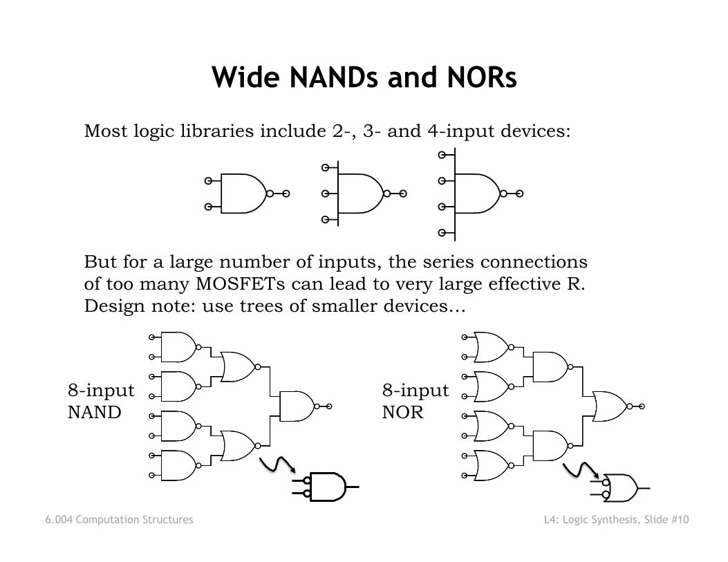
6.004 Computation Structures L4: Logic Synthesis, Slide #10
Wide NANDs and NORs
Most logic libraries include 2-, 3- and 4-input devices:
But for a large number of inputs, the series connections of too many MOSFETs can lead to very large effective R. Design note: use trees of smaller devices…
8-input NAND
8-input NOR

6.004 Computation Structures L4: Logic Synthesis, Slide #11
CMOS Sum-of-products Implementation
AB=A+B
NAND-NAND
NOR-NOR
C
A
B
Y ≡ C
A
B
Y
AC + AB + BC
≡ C
A
BY
AC + AB + BC
C
A
B
Y
C
A
BY
AB=A+B “Pushing Bubbles”
C
A
BY
You might think all these extra inverters would make this structure less attractive. However, quite the opposite is true.
6.004 Computation Structures L4: Logic Synthesis, Slide #12
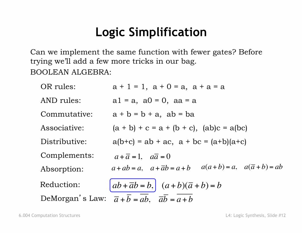
Can we implement the same function with fewer gates? Before trying we’ll add a few more tricks in our bag.
BOOLEAN ALGEBRA:
OR rules: a + 1 = 1, a + 0 = a, a + a = a
AND rules: a1 = a, a0 = 0, aa = a
Commutative: a + b = b + a, ab = ba
Associative: (a + b) + c = a + (b + c), (ab)c = a(bc)
Distributive: a(b+c) = ab + ac, a + bc = (a+b)(a+c)
Complements:
Absorption:
Reduction:
DeMorgan’s Law:
a+ a =1, aa = 0a+ ab = a, a+ ab = a+ b a(a+ b) = a, a(a + b) = ab
ab+ ab = b, (a+ b)(a + b) = ba + b = ab, ab = a+ b
Logic Simplification

6.004 Computation Structures L4: Logic Synthesis, Slide #13
BACCBAACBABCY +++=
Let’s (again!) simplify
Using the identity
αA+αA =α(A+ A) =α ⋅1=α
BACCBAACBABCY +++=
CBACY +=
BACCBABCY ++=
Can’t he come up with a new example???
For any expression α and variable A:
Boolean Minimization
Hey… I could write a program to do
that

6.004 Computation Structures L4: Logic Synthesis, Slide #14
C B A Y
0 0 0 0
0 0 1 1
0 1 0 0
0 1 1 1
1 0 0 0
1 0 1 0
1 1 0 1
1 1 1 1
�
CA
�
CB
�
BA
C B A Y
0 X 0 0
0 X 1 1
1 0 X 0
1 1 X 1
X 0 0 0
X 1 1 1
One way to reveal the opportunities for a more compact implementation is to rewrite the truth table using “don’t cares” (-- or X) to indicate when the value of a particular input is irrelevant in determining the value of the output.
Truth Tables with “Don’t Cares”
Note: Some input combinations (e.g., 000) are matched by more than one row in the “don’t care” table. It would be a bug if all the matching rows didn’t specify the same output value!

6.004 Computation Structures L4: Logic Synthesis, Slide #15
Y =CA+CB+ AB
A C
B
Y
NOTE: The steady state behavior of these circuits is identical. They differ in their transient behavior.
Y(1) C(1)
�
Y = C A + CB
A(1)
B(1)
0 0
1
C B A Y
0 0 0 0
0 0 1 1
0 1 0 0
0 1 1 1
1 0 0 0
1 0 1 0
1 1 0 1
1 1 1 1
�
CA
�
CB
�
BA
The Case for a Non-minimal SOP
A B C Y
That’s what we call a
“glitch” or “hazard”
A B C Y
Now it’s LENIENT!

6.004 Computation Structures L4: Logic Synthesis, Slide #16
It’s cyclic. The left edge is adjacent to the right edge. (It’s really just a flattened out cube).
C\AB 00 01 11 10
0 0 0 1 1
1 0 1 1 0
000 001
010 011
100 101
110 111
Here’s the layout of a 3-variable K-map filled in with the values from our truth table:
K-Map: a truth table arranged so that terms which differ by exactly one variable are adjacent to one another so we can see potential reductions easily.
C B A Y
0 0 0 0
0 0 1 1
0 1 0 0
0 1 1 1
1 0 0 0
1 0 1 0
1 1 0 1
1 1 1 1
Truth Table
Why did he shade that row Gray?
Karnaugh Maps: A Geometric Approach

6.004 Computation Structures L4: Logic Synthesis, Slide #17
4-variable K-map F(A,B,C,D):
Again it’s cyclic. The left edge is adjacent to the right edge, and the top is adjacent to the bottom.
\AB CD\ 00 01 11 10 00 0 1 1 1 01 1 1 1 1 11 1 1 1 1 10 1 0 0 1
Extending K-maps to 4-variable Tables
For functions of 5 or 6 variables, we’d need to use the 3rd dimension to build a 4x4x4 K-map. But then we’re out of dimensions…
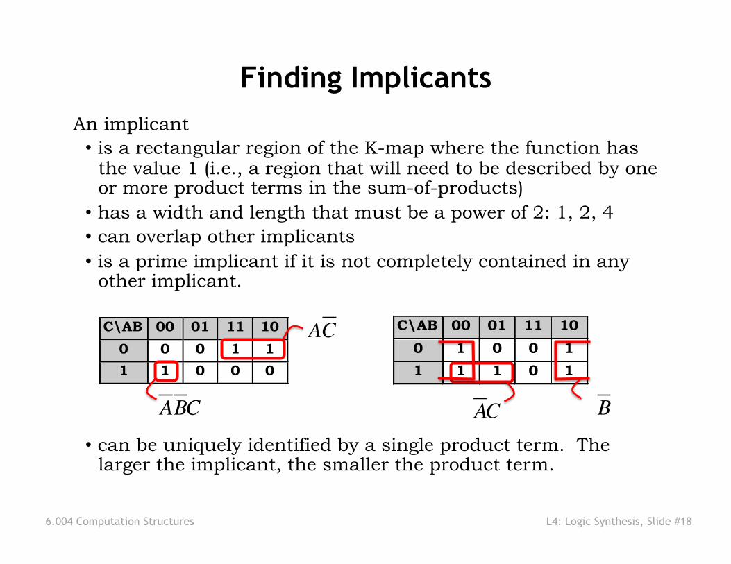
6.004 Computation Structures L4: Logic Synthesis, Slide #18
An implicant • is a rectangular region of the K-map where the function has
the value 1 (i.e., a region that will need to be described by one or more product terms in the sum-of-products)
• has a width and length that must be a power of 2: 1, 2, 4 • can overlap other implicants • is a prime implicant if it is not completely contained in any
other implicant.
• can be uniquely identified by a single product term. The larger the implicant, the smaller the product term.
Finding Implicants
C\AB 00 01 11 10
0 1 0 0 1
1 1 1 0 1
ACC\AB 00 01 11 10
0 0 0 1 1
1 1 0 0 0
ABC AC B

6.004 Computation Structures L4: Logic Synthesis, Slide #19
We want to find all the prime implicants. The right strategy is a greedy one.
• Find the uncircled prime implicant with the greatest area – Order: 4x4 ⇒ 2x4 or 4x2 ⇒ 4x1 or 1x4 or 2x2 ⇒ 2x1 or 1x2 ⇒ 1x1 – Overlap is okay
• Circle it • Repeat until all prime implicants are circled
\AB CD\ 00 01 11 10 00 0 1 1 1 01 1 1 1 1 11 1 1 1 1 10 1 0 0 1
Finding Prime Implicants

6.004 Computation Structures L4: Logic Synthesis, Slide #20
Picking just enough prime implicants to cover all the 1’s in the KMap, combine equations to form minimal sum-of-products.
C\AB 00 01 11 10
0 0 0 1 1
1 0 1 1 0
Write Down Equations
We’re done!
\AB CD\ 00 01 11 10 00 0 1 1 1 01 1 1 1 1 11 1 1 1 1 10 1 0 0 1
Y = AC +BC
Y = D+BC + AC +BC \AB CD\ 00 01 11 10 00 0 1 1 1 01 1 1 1 1 11 1 1 1 1 10 1 0 0 1
Y = D+BC + AB+BC
Minimal SOP is not necessarily unique!

6.004 Computation Structures L4: Logic Synthesis, Slide #21
C\AB 00 01 11 10
0 0 0 1 1
1 0 1 1 0
Prime Implicants, Glitches & Leniency
�
Y = C A + CBC A
B
A B C Y
This circuit produces a glitch on Y when A=1, B=1, C: 1→0
To make the circuit lenient, include product terms for ALL prime implicants.
Y =CA+CB+ AB
A C
B

6.004 Computation Structures L4: Logic Synthesis, Slide #22
D0
D1
S
… and implemented as a tree of smaller MUXes:
MUXes can be generalized to 2k data inputs and k select inputs …
2-input Multiplexer
Y S D1 D0 Y 0 0 0 0 0 0 1 1 0 1 0 0 0 1 1 1 1 0 0 0 1 0 1 0 1 1 0 1 1 1 1 1
Truth Table
We’ve Been Designing a Mux
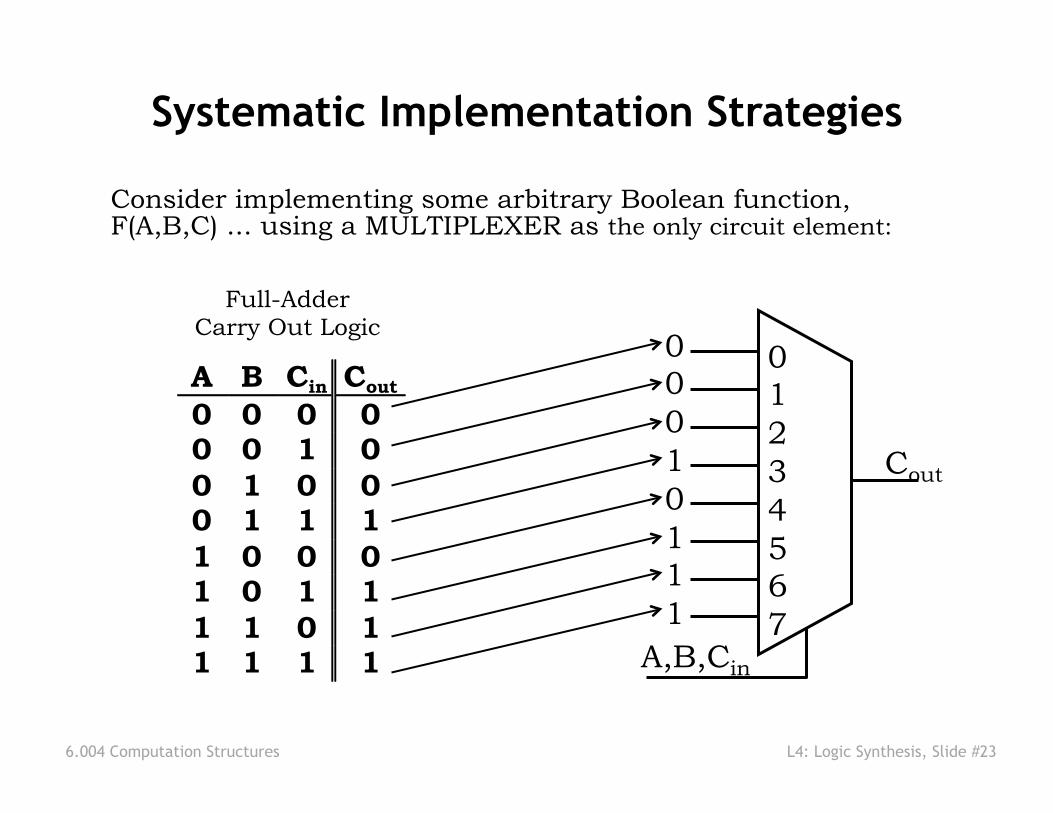
6.004 Computation Structures L4: Logic Synthesis, Slide #23
Consider implementing some arbitrary Boolean function, F(A,B,C) ... using a MULTIPLEXER as the only circuit element:
A B Cin Cout 0 0 0 0 0 0 1 0 0 1 0 0 0 1 1 1 1 0 0 0 1 0 1 1 1 1 0 1 1 1 1 1
Full-Adder Carry Out Logic
0 1 2 3 4 5 6 7
A,B,Cin
Cout
0 0 0 1 0 1 1 1
Systematic Implementation Strategies
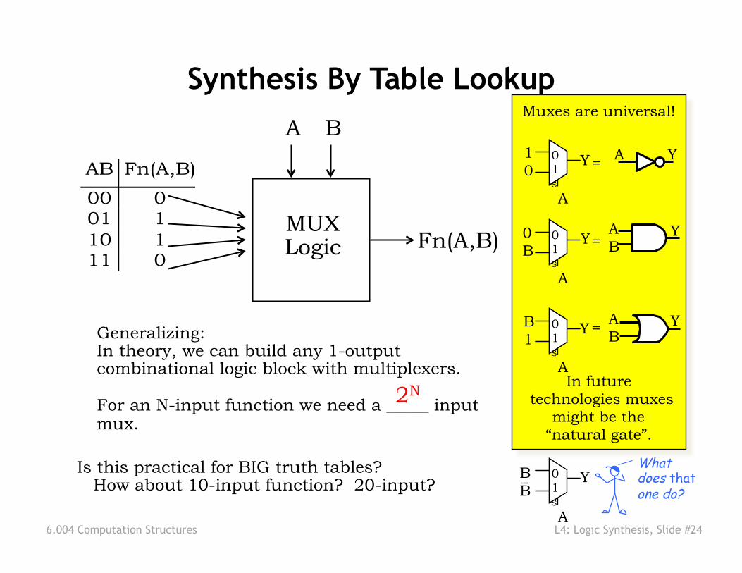
6.004 Computation Structures L4: Logic Synthesis, Slide #24
MUX Logic
A B
Fn(A,B)
Generalizing: In theory, we can build any 1-output combinational logic block with multiplexers. For an N-input function we need a _____ input mux.
AB Fn(A,B)
00 0 01 1 10 1 11 0
2N
Muxes are universal!
In future technologies muxes
might be the “natural gate”.
0 1 0 1S
1 0
A
Y A Y =
0 1 0 1S
0 B
A
Y
0 1 0 1S
B 1
A
Y
=
=
A B
Y
A B
Y
Is this practical for BIG truth tables? How about 10-input function? 20-input?
Synthesis By Table Lookup
0 1 0 1S
B B
A
Y What does that one do?

6.004 Computation Structures L4: Logic Synthesis, Slide #25
k
D0 D1
DN-1
DECODER:
• k SELECT inputs,
• N = 2k DATA OUTPUTs.
Select inputs choose one of the Dj to assert HIGH, all others will be LOW.
NOW, we are well on our way to building a general purpose table-lookup device. We can build a 2-dimensional ARRAY of decoders and selectors as follows ...
Have I mentioned that HIGH
is a synonym for ‘1’ and LOW means
the same as ‘0’
A New Combinational Device

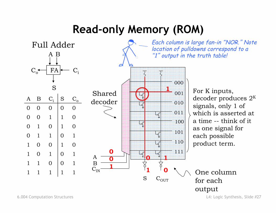
6.004 Computation Structures L4: Logic Synthesis, Slide #26
COUT S
000
001
010
011
100
101
110
111 A B CIN
A B Ci S Co
0 0 0 0 0
0 0 1 1 0
0 1 0 1 0
0 1 1 0 1
1 0 0 1 0
1 0 1 0 1
1 1 0 0 1
1 1 1 1 1
FA
A B
Co Ci
S
Full Adder
For K inputs, decoder produces 2K signals, only 1 of which is asserted at a time -- think of it as one signal for each possible product term.
Each column is large fan-in “NOR.” Note location of pulldowns correspond to a “1” output in the truth table!
Shared decoder
One column for each output
Read-only Memory (ROM)
6.004 Computation Structures L4: Logic Synthesis, Slide #27
COUT S
000
001
010
011
100
101
110
111 A B CIN
A B Ci S Co
0 0 0 0 0
0 0 1 1 0
0 1 0 1 0
0 1 1 0 1
1 0 0 1 0
1 0 1 0 1
1 1 0 0 1
1 1 1 1 1
FA
A B
Co Ci
S
Full Adder
For K inputs, decoder produces 2K signals, only 1 of which is asserted at a time -- think of it as one signal for each possible product term.
Each column is large fan-in “NOR.” Note location of pulldowns correspond to a “1” output in the truth table!
Shared decoder
One column for each output
Read-only Memory (ROM)
0 0 1
1
0 1
0 1

6.004 Computation Structures L4: Logic Synthesis, Slide #28
FA
A B
Co Ci
S
Full Adder LONG LINES slow down propagation times…
The best way to improve this is to build square arrays, using some inputs to drive output selectors (MUXes):
00
01
10
11
0 1 0 1 A B CIN
COUT S
2D Addressing: Standard for ROMs, RAMs, logic arrays…
Read-only Memory (ROM)
A B Ci S Co
0 0 0 0 0
0 0 1 1 0
0 1 0 1 0
0 1 1 0 1
1 0 0 1 0
1 0 1 0 1
1 1 0 0 1
1 1 1 1 1

6.004 Computation Structures L4: Logic Synthesis, Slide #29
ROMs ignore the structure of combinational functions ... • Size, layout, and design are independent of function • Any Truth table can be “programmed” by minor reconfiguration:
- Metal layer (masked ROMs) - Fuses (Field-programmable PROMs) - Charge on floating gates (EPROMs) ... etc.
Model: LOOK UP value of function in truth table...
Inputs: “ADDRESS” of a T.T. entry ROM SIZE = # TT entries... ... for an N-input boolean function, size ≅ __________
2N x #outputs
ROMs tend to generate “glitchy” outputs. WHY?
Logic According to ROMs
6.004 Computation Structures L4: Logic Synthesis, Slide #30
• Sum of products • Any function that can be specified by a truth table or,
equivalently, in terms of AND/OR/NOT (Boolean expression)
• “3-level” implementation of any logic function
• Limitations on number of inputs (fan-in) increases depth
• SOP implementation methods
• NAND-NAND, NOR-NOR
• Muxes used to build table-lookup implementations • Easy to change implemented function -- just change
constants
• ROMs • Decoder logic generates all possible product terms
• Selector logic determines which terms are ORed together
Summary