Embed Size (px)
Citation preview
74LVC1G14Single Schmitt-trigger inverterRev. 15 — 8 June 2018 Product data sheet
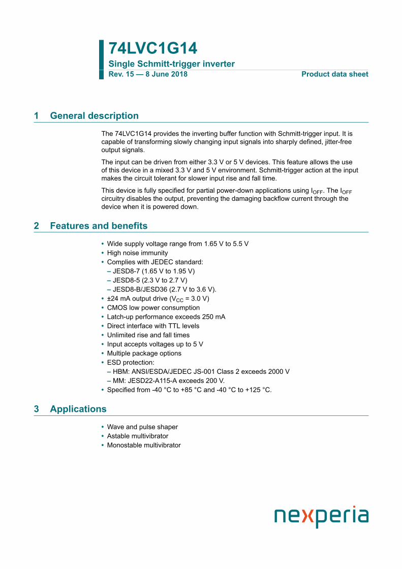
1 General description
The 74LVC1G14 provides the inverting buffer function with Schmitt-trigger input. It iscapable of transforming slowly changing input signals into sharply defined, jitter-freeoutput signals.
The input can be driven from either 3.3 V or 5 V devices. This feature allows the useof this device in a mixed 3.3 V and 5 V environment. Schmitt-trigger action at the inputmakes the circuit tolerant for slower input rise and fall time.
This device is fully specified for partial power-down applications using IOFF. The IOFFcircuitry disables the output, preventing the damaging backflow current through thedevice when it is powered down.
2 Features and benefits
• Wide supply voltage range from 1.65 V to 5.5 V• High noise immunity• Complies with JEDEC standard:
– JESD8-7 (1.65 V to 1.95 V)– JESD8-5 (2.3 V to 2.7 V)– JESD8-B/JESD36 (2.7 V to 3.6 V).
• ±24 mA output drive (VCC = 3.0 V)• CMOS low power consumption• Latch-up performance exceeds 250 mA• Direct interface with TTL levels• Unlimited rise and fall times• Input accepts voltages up to 5 V• Multiple package options• ESD protection:
– HBM: ANSI/ESDA/JEDEC JS-001 Class 2 exceeds 2000 V– MM: JESD22-A115-A exceeds 200 V.
• Specified from -40 °C to +85 °C and -40 °C to +125 °C.
3 Applications
• Wave and pulse shaper• Astable multivibrator• Monostable multivibrator
Nexperia 74LVC1G14Single Schmitt-trigger inverter
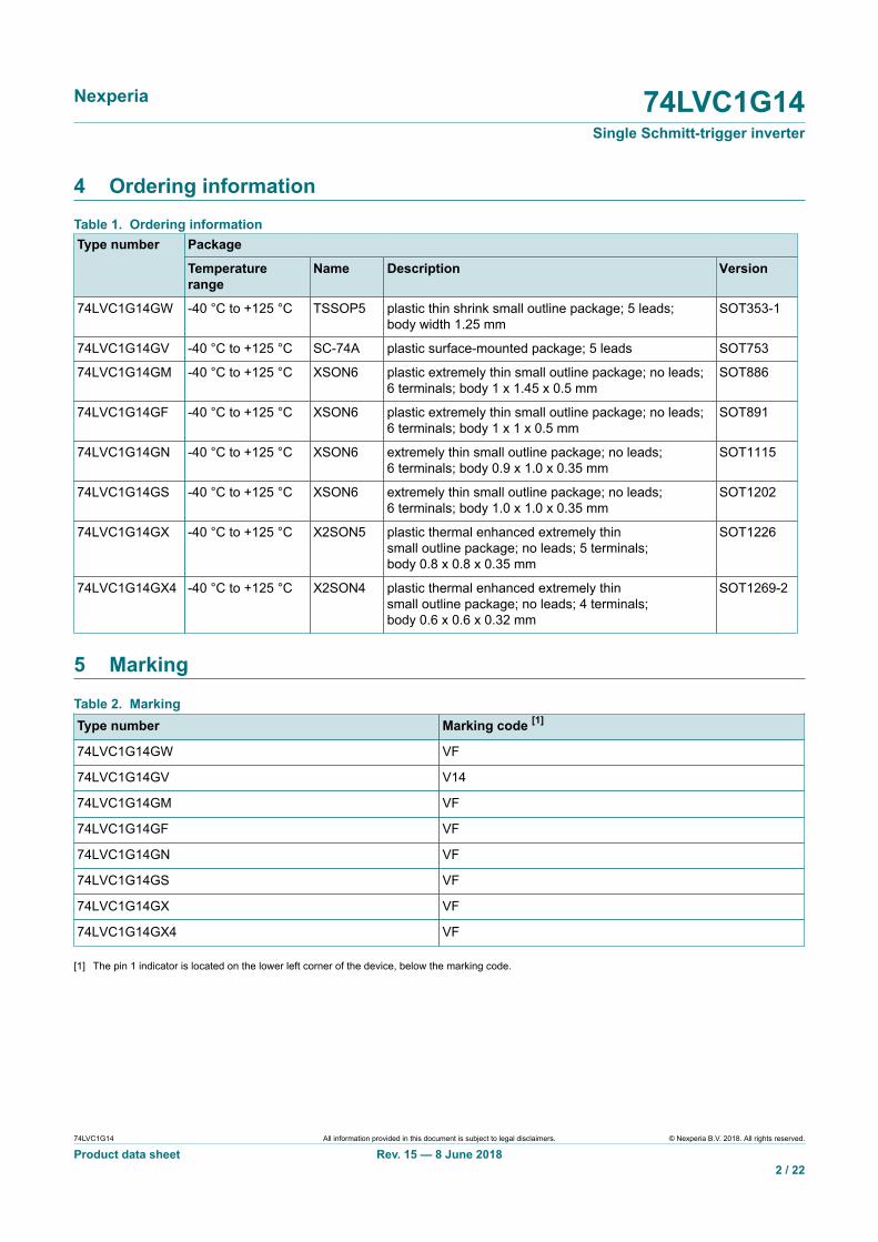
4 Ordering informationTable 1. Ordering information
PackageType number
Temperaturerange
Name Description Version
74LVC1G14GW -40 °C to +125 °C TSSOP5 plastic thin shrink small outline package; 5 leads;body width 1.25 mm
SOT353-1
74LVC1G14GV -40 °C to +125 °C SC-74A plastic surface-mounted package; 5 leads SOT753
74LVC1G14GM -40 °C to +125 °C XSON6 plastic extremely thin small outline package; no leads;6 terminals; body 1 x 1.45 x 0.5 mm
SOT886
74LVC1G14GF -40 °C to +125 °C XSON6 plastic extremely thin small outline package; no leads;6 terminals; body 1 x 1 x 0.5 mm
SOT891
74LVC1G14GN -40 °C to +125 °C XSON6 extremely thin small outline package; no leads;6 terminals; body 0.9 x 1.0 x 0.35 mm
SOT1115
74LVC1G14GS -40 °C to +125 °C XSON6 extremely thin small outline package; no leads;6 terminals; body 1.0 x 1.0 x 0.35 mm
SOT1202
74LVC1G14GX -40 °C to +125 °C X2SON5 plastic thermal enhanced extremely thinsmall outline package; no leads; 5 terminals;body 0.8 x 0.8 x 0.35 mm
SOT1226
74LVC1G14GX4 -40 °C to +125 °C X2SON4 plastic thermal enhanced extremely thinsmall outline package; no leads; 4 terminals;body 0.6 x 0.6 x 0.32 mm
SOT1269-2
5 Marking
Table 2. MarkingType number Marking code [1]
74LVC1G14GW VF
74LVC1G14GV V14
74LVC1G14GM VF
74LVC1G14GF VF
74LVC1G14GN VF
74LVC1G14GS VF
74LVC1G14GX VF
74LVC1G14GX4 VF
[1] The pin 1 indicator is located on the lower left corner of the device, below the marking code.
74LVC1G14 All information provided in this document is subject to legal disclaimers. © Nexperia B.V. 2018. All rights reserved.
Product data sheet Rev. 15 — 8 June 20182 / 22
Nexperia 74LVC1G14Single Schmitt-trigger inverter
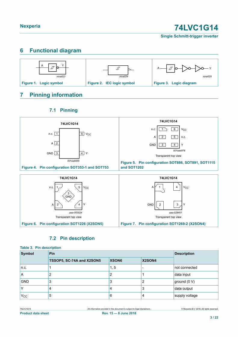
6 Functional diagram
mna023
A Y
Figure 1. Logic symbol
mna024
Figure 2. IEC logic symbol
mna025
A Y
Figure 3. Logic diagram
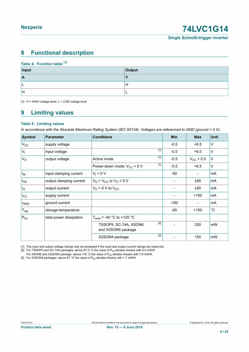
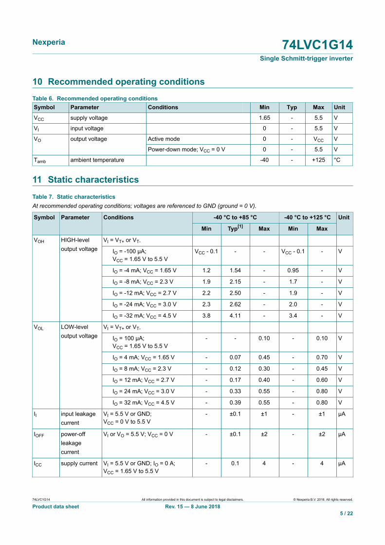
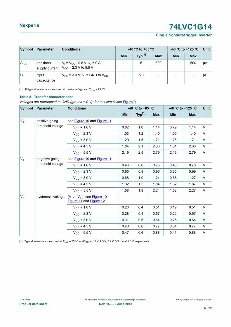
7 Pinning information
7.1 Pinning
74LVC1G14
n.c. VCC
A
GND Y
001aab655
1
2
3
5
4
Figure 4. Pin configuration SOT353-1 and SOT753
74LVC1G14
A
001aae976
n.c.
GND
n.c.
VCC
Y
Transparent top view
2
3
1
5
4
6
Figure 5. Pin configuration SOT886, SOT891, SOT1115and SOT1202
n.c. VCC
GND
1
3
2
5
4A Y
aaa-003024
Transparent top view
74LVC1G14
Figure 6. Pin configuration SOT1226 (X2SON5)
aaa-028401
Transparent top view
74LVC1G14
VCC4
Y3
A 1
GND 2
Figure 7. Pin configuration SOT1269-2 (X2SON4)
7.2 Pin description
Table 3. Pin descriptionPinSymbol
TSSOP5, SC-74A and X2SON5 XSON6 X2SON4
Description
n.c. 1 1, 5 - not connected
A 2 2 1 data input
GND 3 3 2 ground (0 V)
Y 4 4 3 data output
VCC 5 6 4 supply voltage
74LVC1G14 All information provided in this document is subject to legal disclaimers. © Nexperia B.V. 2018. All rights reserved.
Product data sheet Rev. 15 — 8 June 20183 / 22
Nexperia 74LVC1G14Single Schmitt-trigger inverter
8 Functional description
Table 4. Function table [1]
Input Output
A Y
L H
H L
[1] H = HIGH voltage level; L = LOW voltage level
9 Limiting values
Table 5. Limiting valuesIn accordance with the Absolute Maximum Rating System (IEC 60134). Voltages are referenced to GND (ground = 0 V).
Symbol Parameter Conditions Min Max Unit
VCC supply voltage -0.5 +6.5 V
VI input voltage [1] -0.5 +6.5 V
Active mode [1] -0.5 VCC + 0.5 VVO output voltage
Power-down mode; VCC = 0 V [1] -0.5 +6.5 V
IIK input clamping current VI < 0 V -50 - mA
IOK output clamping current VO > VCC or VO < 0 V - ±50 mA
IO output current VO = 0 V to VCC - ±50 mA
ICC supply current - +100 mA
IGND ground current -100 - mA
Tstg storage temperature -65 +150 °C
Tamb = -40 °C to +125 °C
TSSOP5, SC-74A, XSON6and X2SON5 package
[2] - 250 mW
Ptot total power dissipation
X2SON4 package [3] - 150 mW
[1] The input and output voltage ratings may be exceeded if the input and output current ratings are observed.[2] For TSSOP5 and SC-74A packages: above 87.5 °C the value of Ptot derates linearly with 4.0 mW/K.
For XSON6 and X2SON5 package: above 118 °C the value of Ptot derates linearly with 7.8 mW/K.[3] For X2SON4 packages: above 57 °C the value of Ptot derates linearly with 1.7 mW/K.
74LVC1G14 All information provided in this document is subject to legal disclaimers. © Nexperia B.V. 2018. All rights reserved.
Product data sheet Rev. 15 — 8 June 20184 / 22
Nexperia 74LVC1G14Single Schmitt-trigger inverter
10 Recommended operating conditionsTable 6. Recommended operating conditionsSymbol Parameter Conditions Min Typ Max Unit
VCC supply voltage 1.65 - 5.5 V
VI input voltage 0 - 5.5 V
Active mode 0 - VCC VVO output voltage
Power-down mode; VCC = 0 V 0 - 5.5 V
Tamb ambient temperature -40 - +125 °C
11 Static characteristics
Table 7. Static characteristicsAt recommended operating conditions; voltages are referenced to GND (ground = 0 V).
-40 °C to +85 °C -40 °C to +125 °CSymbol Parameter Conditions
Min Typ[1] Max Min Max
Unit
VI = VT+ or VT-
IO = -100 μA;VCC = 1.65 V to 5.5 V
VCC - 0.1 - - VCC - 0.1 - V
IO = -4 mA; VCC = 1.65 V 1.2 1.54 - 0.95 - V
IO = -8 mA; VCC = 2.3 V 1.9 2.15 - 1.7 - V
IO = -12 mA; VCC = 2.7 V 2.2 2.50 - 1.9 - V
IO = -24 mA; VCC = 3.0 V 2.3 2.62 - 2.0 - V
VOH HIGH-leveloutput voltage
IO = -32 mA; VCC = 4.5 V 3.8 4.11 - 3.4 - V
VI = VT+ or VT-
IO = 100 μA;VCC = 1.65 V to 5.5 V
- - 0.10 - 0.10 V
IO = 4 mA; VCC = 1.65 V - 0.07 0.45 - 0.70 V
IO = 8 mA; VCC = 2.3 V - 0.12 0.30 - 0.45 V
IO = 12 mA; VCC = 2.7 V - 0.17 0.40 - 0.60 V
IO = 24 mA; VCC = 3.0 V - 0.33 0.55 - 0.80 V
VOL LOW-leveloutput voltage
IO = 32 mA; VCC = 4.5 V - 0.39 0.55 - 0.80 V
II input leakagecurrent
VI = 5.5 V or GND;VCC = 0 V to 5.5 V
- ±0.1 ±1 - ±1 μA
IOFF power-offleakagecurrent
VI or VO = 5.5 V; VCC = 0 V - ±0.1 ±2 - ±2 μA
ICC supply current VI = 5.5 V or GND; IO = 0 A;VCC = 1.65 V to 5.5 V
- 0.1 4 - 4 μA
74LVC1G14 All information provided in this document is subject to legal disclaimers. © Nexperia B.V. 2018. All rights reserved.
Product data sheet Rev. 15 — 8 June 20185 / 22
Nexperia 74LVC1G14Single Schmitt-trigger inverter
-40 °C to +85 °C -40 °C to +125 °CSymbol Parameter Conditions
Min Typ[1] Max Min Max
Unit
ΔICC additionalsupply current
VI = VCC - 0.6 V; IO = 0 A;VCC = 2.3 V to 5.5 V
- 5 500 - 500 μA
CI inputcapacitance
VCC = 3.3 V; VI = GND to VCC - 5.0 - - - pF
[1] All typical values are measured at maximum VCC and Tamb = 25 °C.
Table 8. Transfer characteristicsVoltages are referenced to GND (ground = 0 V); for test circuit see Figure 9.
-40 °C to +85 °C -40 °C to +125 °CSymbol Parameter Conditions
Min Typ[1] Max Min Max
Unit
see Figure 10 and Figure 11
VCC = 1.8 V 0.82 1.0 1.14 0.79 1.14 V
VCC = 2.3 V 1.03 1.2 1.40 1.00 1.40 V
VCC = 3.0 V 1.29 1.5 1.71 1.26 1.71 V
VCC = 4.5 V 1.84 2.1 2.36 1.81 2.36 V
VT+ positive-goingthreshold voltage
VCC = 5.5 V 2.19 2.5 2.79 2.16 2.79 V
see Figure 10 and Figure 11
VCC = 1.8 V 0.46 0.6 0.75 0.46 0.78 V
VCC = 2.3 V 0.65 0.8 0.96 0.65 0.99 V
VCC = 3.0 V 0.88 1.0 1.24 0.88 1.27 V
VCC = 4.5 V 1.32 1.5 1.84 1.32 1.87 V
VT- negative-goingthreshold voltage
VCC = 5.5 V 1.58 1.8 2.24 1.58 2.27 V
(VT+ - VT-); see Figure 10,Figure 11 and Figure 12
VCC = 1.8 V 0.26 0.4 0.51 0.19 0.51 V
VCC = 2.3 V 0.28 0.4 0.57 0.22 0.57 V
VCC = 3.0 V 0.31 0.5 0.64 0.25 0.64 V
VCC = 4.5 V 0.40 0.6 0.77 0.34 0.77 V
VH hysteresis voltage
VCC = 5.5 V 0.47 0.6 0.88 0.41 0.88 V
[1] Typical values are measured at Tamb = 25 °C and VCC = 1.8 V, 2.5 V, 2.7 V, 3.3 V and 5.0 V respectively.
74LVC1G14 All information provided in this document is subject to legal disclaimers. © Nexperia B.V. 2018. All rights reserved.
Product data sheet Rev. 15 — 8 June 20186 / 22
Nexperia 74LVC1G14Single Schmitt-trigger inverter
12 Dynamic characteristics
Table 9. Dynamic characteristicsVoltages are referenced to GND (ground = 0 V); for test circuit see Figure 9.
-40 °C to +85 °C -40 °C to +125 °CSymbol Parameter Conditions
Min Typ [1] Max Min Max
Unit
A to Y; see Figure 8 [2]
VCC = 1.65 V to 1.95 V 1.0 4.1 11.0 1.0 14.0 ns
VCC = 2.3 V to 2.7 V 0.7 2.8 6.5 0.7 8.5 ns
VCC = 2.7 V 0.7 3.2 6.5 0.7 8.5 ns
VCC = 3.0 V to 3.6 V 0.7 3.0 5.5 0.7 7.0 ns
tpd propagation delay
VCC = 4.5 V to 5.5 V 0.7 2.2 5.0 0.7 6.5 ns
CPD power dissipationcapacitance
VCC = 3.3 V; VI = GND to VCC[3] - 15.4 - - - pF
[1] Typical values are measured at Tamb = 25 °C and VCC = 1.8 V, 2.5 V, 2.7 V, 3.3 V and 5.0 V respectively.[2] tpd is the same as tPLH and tPHL.[3] CPD is used to determine the dynamic power dissipation (PD in μW).
PD = CPD x VCC2 x fi + (CL x VCC
2 x fo) where:fi = input frequency in MHz;fo = output frequency in MHz;CL = output load capacitance in pF;VCC = supply voltage in V.
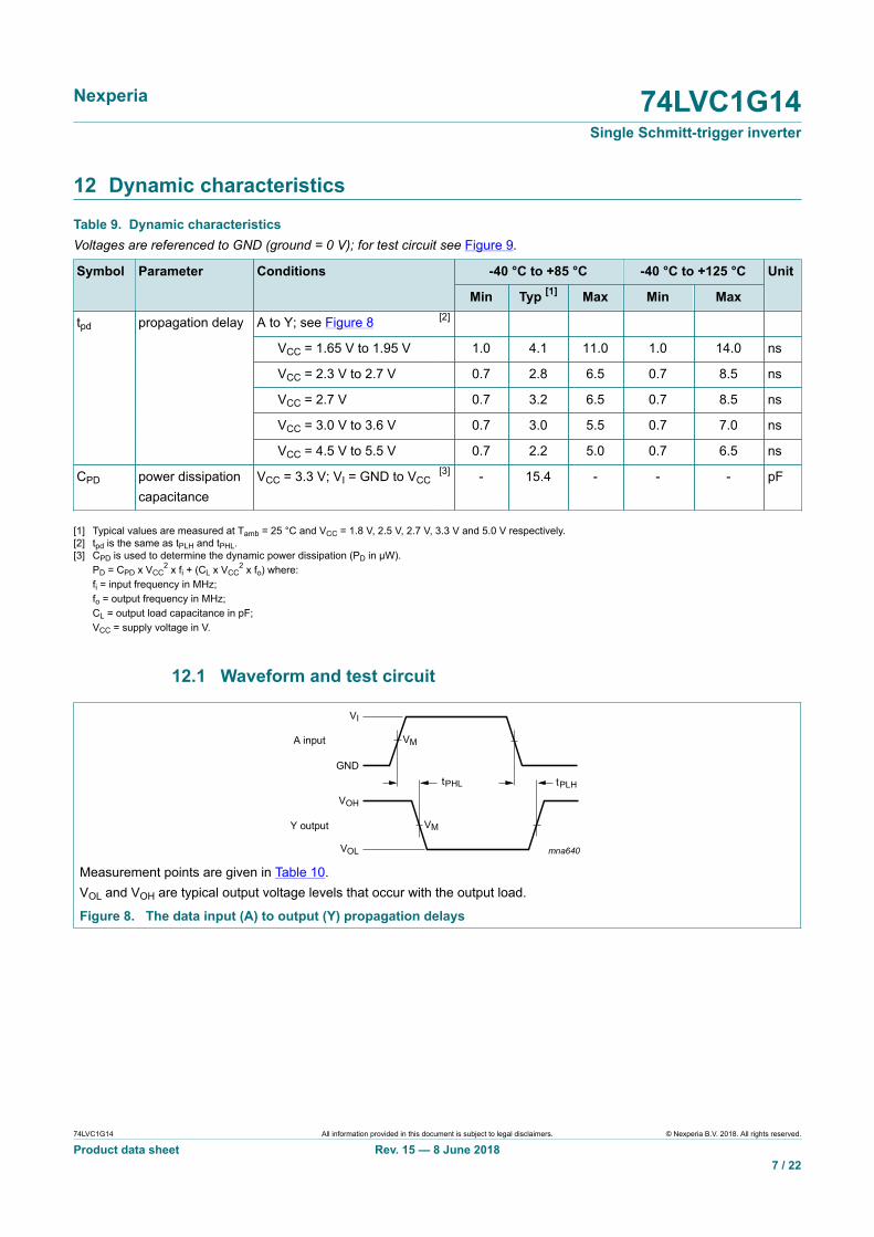
12.1 Waveform and test circuit
mna640
tPHL tPLH
VM
VMA input
Y output
GND
VI
VOH
VOL
Measurement points are given in Table 10.VOL and VOH are typical output voltage levels that occur with the output load.
Figure 8. The data input (A) to output (Y) propagation delays
74LVC1G14 All information provided in this document is subject to legal disclaimers. © Nexperia B.V. 2018. All rights reserved.
Product data sheet Rev. 15 — 8 June 20187 / 22
Nexperia 74LVC1G14Single Schmitt-trigger inverter
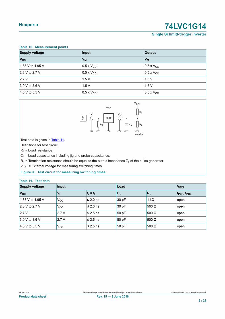
Table 10. Measurement pointsSupply voltage Input Output
VCC VM VM
1.65 V to 1.95 V 0.5 x VCC 0.5 x VCC
2.3 V to 2.7 V 0.5 x VCC 0.5 x VCC
2.7 V 1.5 V 1.5 V
3.0 V to 3.6 V 1.5 V 1.5 V
4.5 V to 5.5 V 0.5 x VCC 0.5 x VCC
VEXT
VCC
VI VO
mna616
DUT
CLRT
RL
RL
G
Test data is given in Table 11.Definitions for test circuit:RL = Load resistance.CL = Load capacitance including jig and probe capacitance.RT = Termination resistance should be equal to the output impedance Zo of the pulse generator.VEXT = External voltage for measuring switching times.
Figure 9. Test circuit for measuring switching times
Table 11. Test dataSupply voltage Input Load VEXT
VCC VI tr = tf CL RL tPLH, tPHL
1.65 V to 1.95 V VCC ≤ 2.0 ns 30 pF 1 kΩ open
2.3 V to 2.7 V VCC ≤ 2.0 ns 30 pF 500 Ω open
2.7 V 2.7 V ≤ 2.5 ns 50 pF 500 Ω open
3.0 V to 3.6 V 2.7 V ≤ 2.5 ns 50 pF 500 Ω open
4.5 V to 5.5 V VCC ≤ 2.5 ns 50 pF 500 Ω open
74LVC1G14 All information provided in this document is subject to legal disclaimers. © Nexperia B.V. 2018. All rights reserved.
Product data sheet Rev. 15 — 8 June 20188 / 22

Nexperia 74LVC1G14Single Schmitt-trigger inverter
12.2 Waveforms transfer characteristics
mna207
VO
VIVH
VT+VT-
Figure 10. Transfer characteristic
mna208
VO
VI VH
VT+
VT-
VT+ and VT- limits at 70 % and 20 %.
Figure 11. Definition of VT+, VT- and VH
0 3VI (V)
ICC (mA)
10
0
2
mna641
4
6
8
1 2
VCC = 3.0 V.
Figure 12. Typical transfer characteristics
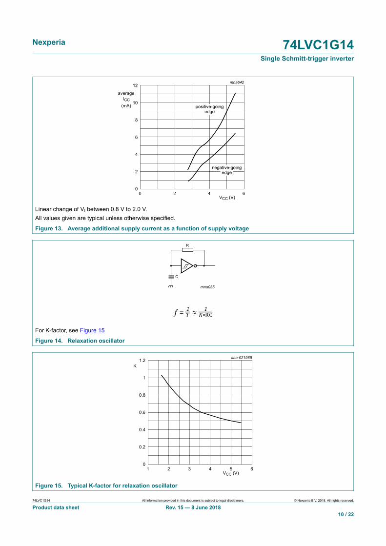
13 Application information
The slow input rise and fall times cause additional power dissipation, this can becalculated using the following formula:
Padd = fi x (tr x ΔICC(AV) + tf x ΔICC(AV)) x VCC where:
• Padd = additional power dissipation (μW);• fi = input frequency (MHz);• tr = input rise time (ns); 10 % to 90 %;• tf = input fall time (ns); 90 % to 10 %;• ΔICC(AV) = average additional supply current (μA).
Average ΔICC(AV) differs with positive or negative input transitions, as shown in Figure 13.
An example of a relaxation circuit using the 74LVC1G14 is shown in Figure 14.
74LVC1G14 All information provided in this document is subject to legal disclaimers. © Nexperia B.V. 2018. All rights reserved.
Product data sheet Rev. 15 — 8 June 20189 / 22
Nexperia 74LVC1G14Single Schmitt-trigger inverter
0 2 6
12
0
8
6
4
2
10
mna642
4VCC (V)
average ICC
(mA)
negative-going edge
positive-going edge
Linear change of VI between 0.8 V to 2.0 V.All values given are typical unless otherwise specified.
Figure 13. Average additional supply current as a function of supply voltage
mna035
R
C
For K-factor, see Figure 15
Figure 14. Relaxation oscillator
aaa-021985
1 2 3 4 5 60
0.2
0.4
0.6
0.8
1
1.2
VCC (V)
KK
Figure 15. Typical K-factor for relaxation oscillator
74LVC1G14 All information provided in this document is subject to legal disclaimers. © Nexperia B.V. 2018. All rights reserved.
Product data sheet Rev. 15 — 8 June 201810 / 22
Nexperia 74LVC1G14Single Schmitt-trigger inverter
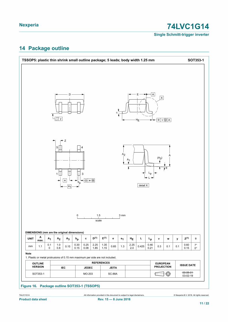
14 Package outline
UNIT A1 A
max. A2 A3 bp L HE Lp w y v c e D(1) E(1) Z(1) θ
REFERENCES OUTLINE VERSION
EUROPEAN PROJECTION ISSUE DATE
IEC JEDEC JEITA
mm 0.1 0
1.0 0.8
0.30 0.15
0.25 0.08
2.25 1.85
1.35 1.15 0.65
e1
1.3 2.25 2.0
0.60 0.15
7° 0°
0.1 0.1 0.3 0.425
DIMENSIONS (mm are the original dimensions)
Note 1. Plastic or metal protrusions of 0.15 mm maximum per side are not included.
0.46 0.21
SOT353-1 MO-203 SC-88A 00-09-01 03-02-19
w M bp
D
Z
e
e1
0.15
1 3
5 4
θ
A A2
A1
Lp
(A3)
detail X
L
HE
E
c
v M A
X A
y
1.5 3 mm 0
scale
TSSOP5: plastic thin shrink small outline package; 5 leads; body width 1.25 mm SOT353-1
1.1
Figure 16. Package outline SOT353-1 (TSSOP5)
74LVC1G14 All information provided in this document is subject to legal disclaimers. © Nexperia B.V. 2018. All rights reserved.
Product data sheet Rev. 15 — 8 June 201811 / 22
Nexperia 74LVC1G14Single Schmitt-trigger inverter
REFERENCESOUTLINE VERSION
EUROPEAN PROJECTION ISSUE DATE
IEC JEDEC JEITA
SOT753 SC-74A
w BMbp
D
e
A
A1
Lp
Q
detail X
HE
E
v M A
AB
y
0 1 2 mm
scale
c
X
1 32
45
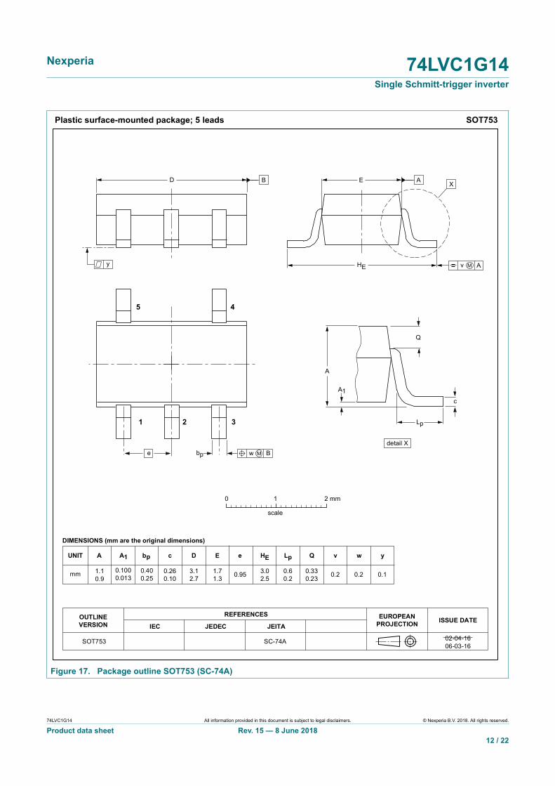
Plastic surface-mounted package; 5 leads SOT753
UNIT A1 bp c D E HE Lp Q ywv
mm 0.100 0.013
0.40 0.25
3.1 2.7
0.26 0.10
1.7 1.3
e
0.95 3.0 2.5 0.2 0.10.2
DIMENSIONS (mm are the original dimensions)
0.6 0.2
0.33 0.23
A
1.1 0.9
02-04-16 06-03-16
Figure 17. Package outline SOT753 (SC-74A)
74LVC1G14 All information provided in this document is subject to legal disclaimers. © Nexperia B.V. 2018. All rights reserved.
Product data sheet Rev. 15 — 8 June 201812 / 22
Nexperia 74LVC1G14Single Schmitt-trigger inverter
ReferencesOutlineversion
Europeanprojection Issue date
IEC JEDEC JEITA
SOT886 MO-252
sot886_po
04-07-2212-01-05
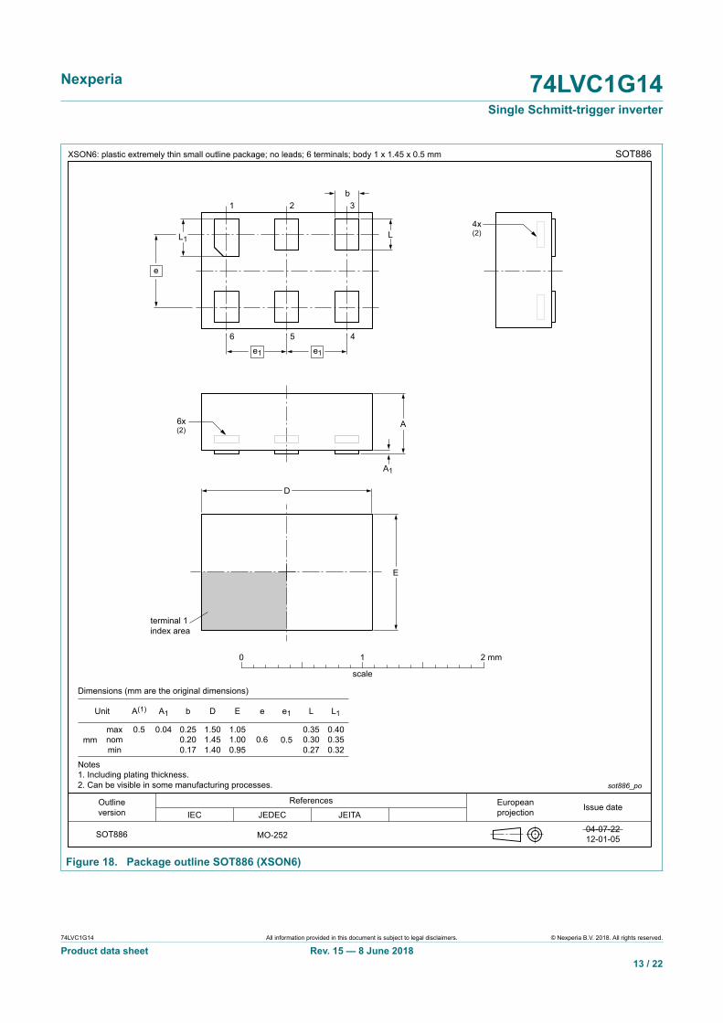
Unit
mmmaxnommin
0.5 0.04 1.501.451.40
1.051.000.95
0.350.300.27
0.400.350.32
0.6
A(1)
Dimensions (mm are the original dimensions)
Notes1. Including plating thickness.2. Can be visible in some manufacturing processes.
XSON6: plastic extremely thin small outline package; no leads; 6 terminals; body 1 x 1.45 x 0.5 mm SOT886
A1 b
0.250.200.17
D E e e1
0.5
L L1
terminal 1index area
D
E
e1
e
A1
b
LL1
e1
0 1 2 mm
scale
1
6
2
5
3
4
6x(2)
4x(2)
A
Figure 18. Package outline SOT886 (XSON6)
74LVC1G14 All information provided in this document is subject to legal disclaimers. © Nexperia B.V. 2018. All rights reserved.
Product data sheet Rev. 15 — 8 June 201813 / 22
Nexperia 74LVC1G14Single Schmitt-trigger inverter
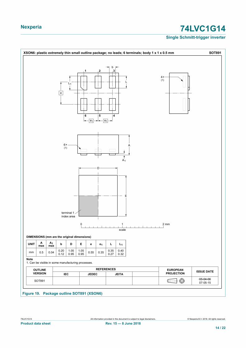
terminal 1 index area
REFERENCESOUTLINE VERSION
EUROPEAN PROJECTION ISSUE DATE
IEC JEDEC JEITA
SOT891
SOT891
05-04-06 07-05-15
XSON6: plastic extremely thin small outline package; no leads; 6 terminals; body 1 x 1 x 0.5 mm
D
E
e1
e
A1
b
LL1
e1
0 1 2 mm
scale
DIMENSIONS (mm are the original dimensions)
UNIT
mm 0.20 0.12
1.05 0.95
0.35 0.27
A1 max b E
1.05 0.95
D e e1 L
0.40 0.32
L1
0.350.55
A max
0.5 0.04
1
6
2
5
3
4
A6× (1)
4× (1)
Note 1. Can be visible in some manufacturing processes.
Figure 19. Package outline SOT891 (XSON6)
74LVC1G14 All information provided in this document is subject to legal disclaimers. © Nexperia B.V. 2018. All rights reserved.
Product data sheet Rev. 15 — 8 June 201814 / 22
Nexperia 74LVC1G14Single Schmitt-trigger inverter
ReferencesOutline version
European projection Issue date
IEC JEDEC JEITA
SOT1115
sot1115_po
10-04-02 10-04-07
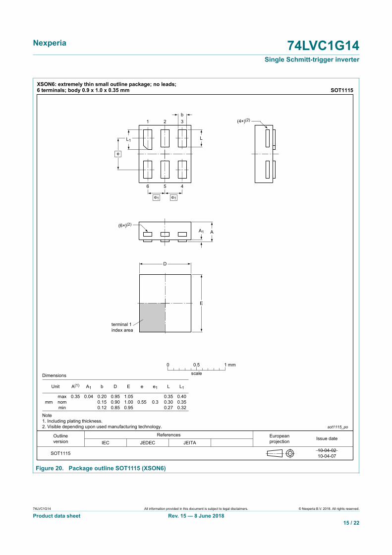
Unit
mmmax nom min
0.35 0.04 0.95 0.90 0.85
1.05 1.00 0.95
0.55 0.30.40 0.35 0.32
A(1)
Dimensions
Note 1. Including plating thickness. 2. Visible depending upon used manufacturing technology.
XSON6: extremely thin small outline package; no leads; 6 terminals; body 0.9 x 1.0 x 0.35 mm SOT1115
A1 b
0.20 0.15 0.12
D E e e1 L
0.35 0.30 0.27
L1
0 0.5 1 mm
scale
terminal 1 index area
D
E
(4×)(2)
e1 e1
e
LL1
b321
6 5 4
(6×)(2)
A1 A
Figure 20. Package outline SOT1115 (XSON6)
74LVC1G14 All information provided in this document is subject to legal disclaimers. © Nexperia B.V. 2018. All rights reserved.
Product data sheet Rev. 15 — 8 June 201815 / 22
Nexperia 74LVC1G14Single Schmitt-trigger inverter
ReferencesOutline version
European projection Issue date
IEC JEDEC JEITA
SOT1202
sot1202_po
10-04-02 10-04-06
Unit
mmmax nom min
0.35 0.04 1.05 1.00 0.95
1.05 1.00 0.95
0.55 0.350.40 0.35 0.32
A(1)
Dimensions
Note 1. Including plating thickness. 2. Visible depending upon used manufacturing technology.
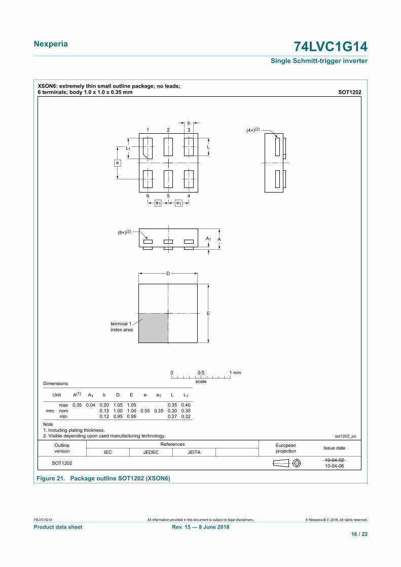
XSON6: extremely thin small outline package; no leads; 6 terminals; body 1.0 x 1.0 x 0.35 mm SOT1202
A1 b
0.20 0.15 0.12
D E e e1 L
0.35 0.30 0.27
L1
0 0.5 1 mm
scale
terminal 1 index area
D
E
(4×)(2)
e1 e1
e
L
b1 2 3
L1
6 5 4
(6×)(2)
AA1
Figure 21. Package outline SOT1202 (XSON6)
74LVC1G14 All information provided in this document is subject to legal disclaimers. © Nexperia B.V. 2018. All rights reserved.
Product data sheet Rev. 15 — 8 June 201816 / 22
Nexperia 74LVC1G14Single Schmitt-trigger inverter
ReferencesOutlineversion
Europeanprojection Issue date
IEC JEDEC EIAJ
SOT1226
sot1226_po
12-04-1012-04-25
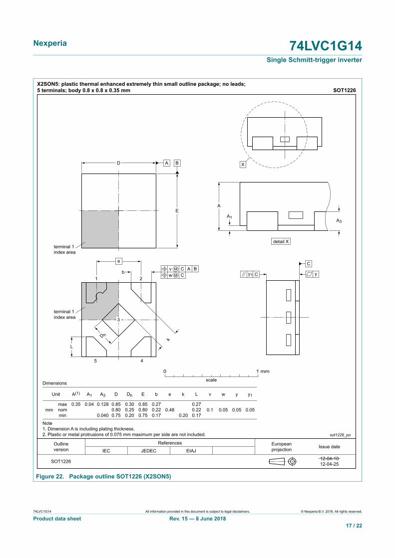
Unit
mmmaxnommin
0.35 0.850.800.75
0.04 0.300.250.20
0.850.800.75
0.270.220.17
0.05
A(1)
Dimensions
Note1. Dimension A is including plating thickness.2. Plastic or metal protrusions of 0.075 mm maximum per side are not included.
SOT1226
A1 A3
0.128
0.040
D Dh E b e
0.48
k L v
0.1
w y
0.05 0.05
scale
0 1 mm
X
terminal 1index area
D
E
A B
detail X
A
A1A3
C
yCy1
5 4
terminal 1index area
D h
L
b
k
e
AC BvCw
21
0.20
0.270.220.17
y1
X2SON5: plastic thermal enhanced extremely thin small outline package; no leads;5 terminals; body 0.8 x 0.8 x 0.35 mm
3
Figure 22. Package outline SOT1226 (X2SON5)
74LVC1G14 All information provided in this document is subject to legal disclaimers. © Nexperia B.V. 2018. All rights reserved.
Product data sheet Rev. 15 — 8 June 201817 / 22
Nexperia 74LVC1G14Single Schmitt-trigger inverter
ReferencesOutlineversion
Europeanprojection Issue date
IEC JEDEC JEITA
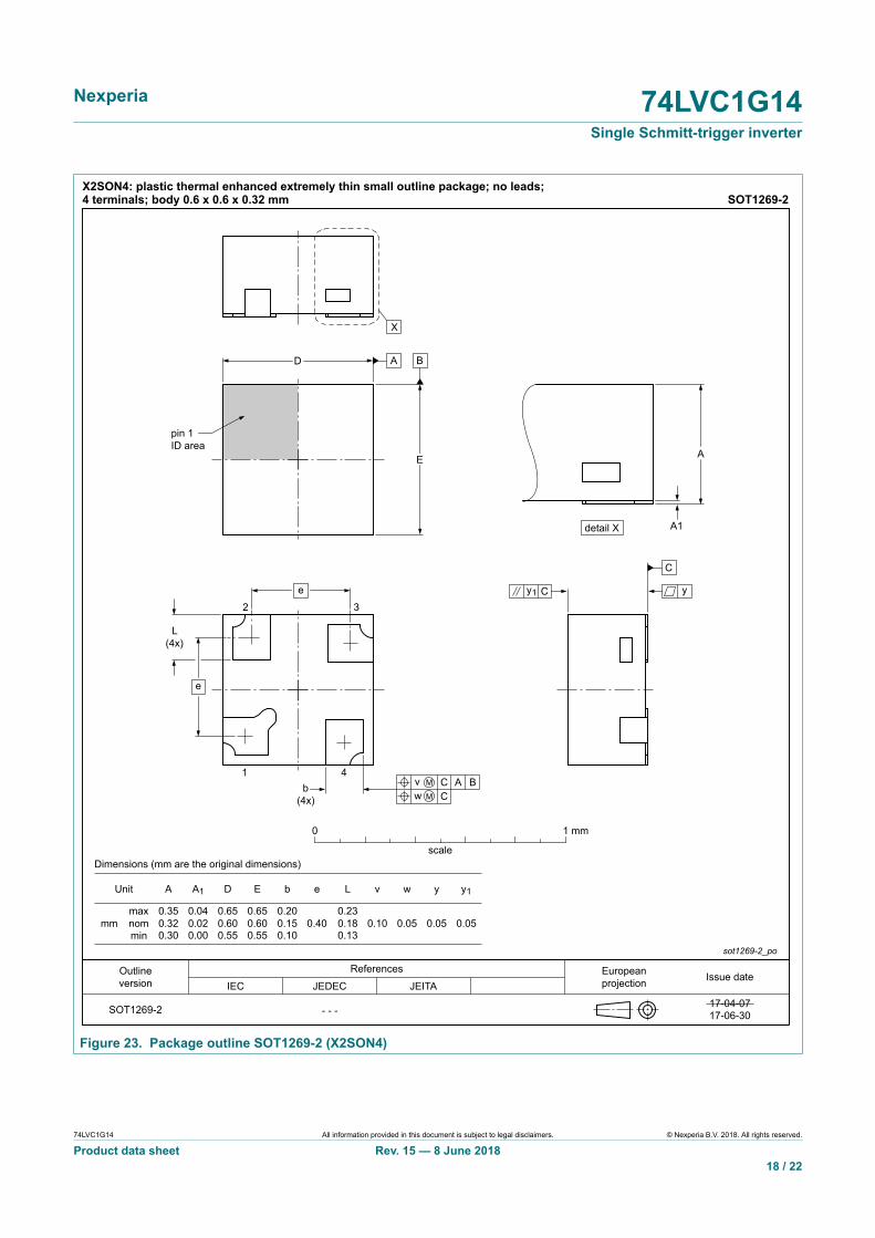
SOT1269-2 - - -
sot1269-2_po
17-04-0717-06-30
Unit
mmmaxnommin
0.35 0.04 0.65 0.200.18 0.10 0.05
A
Dimensions (mm are the original dimensions)
X2SON4: plastic thermal enhanced extremely thin small outline package; no leads;4 terminals; body 0.6 x 0.6 x 0.32 mm SOT1269-2
A1 D
0.65
E b e L v y
0.05
w
0.05
y1
0.32 0.02 0.60 0.15 0.400.600.130.30 0.00 0.55 0.100.55
0.23
0
scale
1 mm
pin 1ID area
1 4
2 3
A BD
E
y
C
Cy1
detail X
A
A1
L(4x)
X
e
e
b(4x)
AC BvCw
Figure 23. Package outline SOT1269-2 (X2SON4)
74LVC1G14 All information provided in this document is subject to legal disclaimers. © Nexperia B.V. 2018. All rights reserved.
Product data sheet Rev. 15 — 8 June 201818 / 22
Nexperia 74LVC1G14Single Schmitt-trigger inverter
15 AbbreviationsTable 12. AbbreviationsAcronym Description
CMOS Complementary Metal Oxide Semiconductor
TTL Transistor-Transistor Logic
HBM Human Body Model
ESD ElectroStatic Discharge
MM Machine Model
DUT Device Under Test
16 Revision historyTable 13. Revision historyDocument ID Release date Data sheet status Change notice Supersedes
74LVC1G14 v.15 20180608 Product data sheet - 74LVC1G14 v.15
Modifications: • The format of this data sheet has been redesigned to comply with the identity guidelines ofNexperia.
• Legal texts have been adapted to the new company name where appropriate.• Added type number 74LVC1G14GX4 (SOT1269-2)
74LVC1G14 v.14 20161202 Product data sheet - 74LVC1G14 v.13
Modifications: • Table 7: The maximum limits for leakage current and supply current have changed.
74LVC1G14 v.13 20160315 Product data sheet - 74LVC1G14 v.12
Modifications: • Figure 15 added (typical K-factor for relaxation oscillator).
74LVC1G14 v.12 20120806 Product data sheet - 74LVC1G14 v.11
Modifications: • Package outline drawing of SOT1226 (Figure 22) modified.
74LVC1G14 v.11 20120412 Product data sheet - 74LVC1G14 v.10
Modifications: • Added type number 74LVC1G14GX (SOT1226)• Package outline drawing of SOT886 (Figure 18) modified.
74LVC1G14 v.10 20111206 Product data sheet - 74LVC1G14 v.9
Modifications: • Legal pages updated.
74LVC1G14 v.9 20110922 Product data sheet - 74LVC1G14 v.8
74LVC1G14 v.8 20101110 Product data sheet - 74LVC1G14 v.7
74LVC1G14 v.7 20070718 Product data sheet - 74LVC1G14 v.6
74LVC1G14 v.6 20060615 Product data sheet - 74LVC1G14 v.5
74LVC1G14 v.5 20040910 Product specification - 74LVC1G14 v.4
74LVC1G14 v.4 20021119 Product specification - 74LVC1G14 v.3
74LVC1G14 v.3 20020521 Product specification - 74LVC1G14 v.2
74LVC1G14 v.2 20010406 Product specification - 74LVC1G14 v.1
74LVC1G14 v.1 20001212 Product specification - -
74LVC1G14 All information provided in this document is subject to legal disclaimers. © Nexperia B.V. 2018. All rights reserved.
Product data sheet Rev. 15 — 8 June 201819 / 22
Nexperia 74LVC1G14Single Schmitt-trigger inverter
17 Legal information
17.1 Data sheet status
Document status[1][2] Product status[3] Definition
Objective [short] data sheet Development This document contains data from the objective specification for productdevelopment.
Preliminary [short] data sheet Qualification This document contains data from the preliminary specification.
Product [short] data sheet Production This document contains the product specification.
[1] Please consult the most recently issued document before initiating or completing a design.[2] The term 'short data sheet' is explained in section "Definitions".[3] The product status of device(s) described in this document may have changed since this document was published and may differ in case of multiple
devices. The latest product status information is available on the Internet at URL http://www.nexperia.com.
17.2 DefinitionsDraft — The document is a draft version only. The content is still underinternal review and subject to formal approval, which may result inmodifications or additions. Nexperia does not give any representations orwarranties as to the accuracy or completeness of information included hereinand shall have no liability for the consequences of use of such information.
Short data sheet — A short data sheet is an extract from a full data sheetwith the same product type number(s) and title. A short data sheet isintended for quick reference only and should not be relied upon to containdetailed and full information. For detailed and full information see therelevant full data sheet, which is available on request via the local Nexperiasales office. In case of any inconsistency or conflict with the short data sheet,the full data sheet shall prevail.
Product specification — The information and data provided in a Productdata sheet shall define the specification of the product as agreed betweenNexperia and its customer, unless Nexperia and customer have explicitlyagreed otherwise in writing. In no event however, shall an agreement bevalid in which the Nexperia product is deemed to offer functions and qualitiesbeyond those described in the Product data sheet.
17.3 DisclaimersLimited warranty and liability — Information in this document is believedto be accurate and reliable. However, Nexperia does not give anyrepresentations or warranties, expressed or implied, as to the accuracyor completeness of such information and shall have no liability for theconsequences of use of such information. Nexperia takes no responsibilityfor the content in this document if provided by an information source outsideof Nexperia. In no event shall Nexperia be liable for any indirect, incidental,punitive, special or consequential damages (including - without limitation -lost profits, lost savings, business interruption, costs related to the removalor replacement of any products or rework charges) whether or not suchdamages are based on tort (including negligence), warranty, breach ofcontract or any other legal theory. Notwithstanding any damages thatcustomer might incur for any reason whatsoever, Nexperia's aggregate andcumulative liability towards customer for the products described herein shallbe limited in accordance with the Terms and conditions of commercial sale ofNexperia.
Right to make changes — Nexperia reserves the right to make changesto information published in this document, including without limitationspecifications and product descriptions, at any time and without notice. Thisdocument supersedes and replaces all information supplied prior to thepublication hereof.
Suitability for use — Nexperia products are not designed, authorized orwarranted to be suitable for use in life support, life-critical or safety-critical
systems or equipment, nor in applications where failure or malfunctionof an Nexperia product can reasonably be expected to result in personalinjury, death or severe property or environmental damage. Nexperia and itssuppliers accept no liability for inclusion and/or use of Nexperia products insuch equipment or applications and therefore such inclusion and/or use is atthe customer’s own risk.
Applications — Applications that are described herein for any of theseproducts are for illustrative purposes only. Nexperia makes no representationor warranty that such applications will be suitable for the specified usewithout further testing or modification. Customers are responsible for thedesign and operation of their applications and products using Nexperiaproducts, and Nexperia accepts no liability for any assistance withapplications or customer product design. It is customer’s sole responsibilityto determine whether the Nexperia product is suitable and fit for thecustomer’s applications and products planned, as well as for the plannedapplication and use of customer’s third party customer(s). Customers shouldprovide appropriate design and operating safeguards to minimize the risksassociated with their applications and products. Nexperia does not acceptany liability related to any default, damage, costs or problem which is basedon any weakness or default in the customer’s applications or products, orthe application or use by customer’s third party customer(s). Customer isresponsible for doing all necessary testing for the customer’s applicationsand products using Nexperia products in order to avoid a default of theapplications and the products or of the application or use by customer’s thirdparty customer(s). Nexperia does not accept any liability in this respect.
Limiting values — Stress above one or more limiting values (as defined inthe Absolute Maximum Ratings System of IEC 60134) will cause permanentdamage to the device. Limiting values are stress ratings only and (proper)operation of the device at these or any other conditions above thosegiven in the Recommended operating conditions section (if present) or theCharacteristics sections of this document is not warranted. Constant orrepeated exposure to limiting values will permanently and irreversibly affectthe quality and reliability of the device.
Terms and conditions of commercial sale — Nexperia products aresold subject to the general terms and conditions of commercial sale, aspublished at http://www.nexperia.com/profile/terms, unless otherwise agreedin a valid written individual agreement. In case an individual agreement isconcluded only the terms and conditions of the respective agreement shallapply. Nexperia hereby expressly objects to applying the customer’s generalterms and conditions with regard to the purchase of Nexperia products bycustomer.
No offer to sell or license — Nothing in this document may be interpretedor construed as an offer to sell products that is open for acceptance orthe grant, conveyance or implication of any license under any copyrights,patents or other industrial or intellectual property rights.
Export control — This document as well as the item(s) described hereinmay be subject to export control regulations. Export might require a priorauthorization from competent authorities.
74LVC1G14 All information provided in this document is subject to legal disclaimers. © Nexperia B.V. 2018. All rights reserved.
Product data sheet Rev. 15 — 8 June 201820 / 22
Nexperia 74LVC1G14Single Schmitt-trigger inverter
Non-automotive qualified products — Unless this data sheet expresslystates that this specific Nexperia product is automotive qualified, theproduct is not suitable for automotive use. It is neither qualified nor tested inaccordance with automotive testing or application requirements. Nexperiaaccepts no liability for inclusion and/or use of non-automotive qualifiedproducts in automotive equipment or applications. In the event that customeruses the product for design-in and use in automotive applications toautomotive specifications and standards, customer (a) shall use the productwithout Nexperia's warranty of the product for such automotive applications,use and specifications, and (b) whenever customer uses the product forautomotive applications beyond Nexperia's specifications such use shall besolely at customer’s own risk, and (c) customer fully indemnifies Nexperiafor any liability, damages or failed product claims resulting from customer
design and use of the product for automotive applications beyond Nexperia'sstandard warranty and Nexperia's product specifications.
Translations — A non-English (translated) version of a document is forreference only. The English version shall prevail in case of any discrepancybetween the translated and English versions.
17.4 TrademarksNotice: All referenced brands, product names, service names andtrademarks are the property of their respective owners.
74LVC1G14 All information provided in this document is subject to legal disclaimers. © Nexperia B.V. 2018. All rights reserved.
Product data sheet Rev. 15 — 8 June 201821 / 22
Nexperia 74LVC1G14Single Schmitt-trigger inverter
Contents1 General description ............................................ 12 Features and benefits .........................................13 Applications .........................................................14 Ordering information .......................................... 25 Marking .................................................................26 Functional diagram ............................................. 37 Pinning information ............................................ 37.1 Pinning ...............................................................37.2 Pin description ................................................... 38 Functional description ........................................49 Limiting values ....................................................410 Recommended operating conditions ................ 511 Static characteristics .......................................... 512 Dynamic characteristics .....................................712.1 Waveform and test circuit ..................................712.2 Waveforms transfer characteristics ....................913 Application information ......................................914 Package outline .................................................1115 Abbreviations .................................................... 1916 Revision history ................................................ 1917 Legal information ..............................................20
Please be aware that important notices concerning this document and the product(s)described herein, have been included in section 'Legal information'.
© Nexperia B.V. 2018. All rights reserved.For more information, please visit: http://www.nexperia.comFor sales office addresses, please send an email to: [email protected]
Date of release: 8 June 2018Document identifier: 74LVC1G14