Embed Size (px)
Citation preview

8-/10-/12-Bit, High Bandwidth Multiplying DACs with Parallel Interface
Data Sheet AD5424/AD5433/AD5445
Rev. E Document Feedback Information furnished by Analog Devices is believed to be accurate and reliable. However, no responsibility is assumed by Analog Devices for its use, nor for any infringements of patents or other rights of third parties that may result from its use. Specifications subject to change without notice. No license is granted by implication or otherwise under any patent or patent rights of Analog Devices. Trademarks and registered trademarks are the property of their respective owners.
One Technology Way, P.O. Box 9106, Norwood, MA 02062-9106, U.S.A. Tel: 781.329.4700 ©2003–2016 Analog Devices, Inc. All rights reserved. Technical Support www.analog.com
FEATURES 2.5 V to 5.5 V supply operation Fast parallel interface (17 ns write cycle) Update rate of 20.4 MSPS INL of ±1 LSB for 12-bit DAC 10 MHz multiplying bandwidth ±10 V reference input Extended temperature range: –40°C to +125°C 20-lead TSSOP and chip scale (4 mm × 4 mm) packages 8-, 10-, and 12-bit current output DACs Upgrades to AD7524/AD7533/AD7545 Pin-compatible 8-, 10-, and 12-bit DACs in chip scale Guaranteed monotonic 4-quadrant multiplication Power-on reset with brownout detection Readback function 0.4 µA typical power consumption
APPLICATIONS Portable battery-powered applications Waveform generators Analog processing Instrumentation applications Programmable amplifiers and attenuators Digitally controlled calibration Programmable filters and oscillators Composite video Ultrasound Gain, offset, and voltage trimming
GENERAL DESCRIPTION The AD5424/AD5433/AD54451 are CMOS 8-, 10-, and 12-bit current output digital-to-analog converters (DACs), respectively. These devices operate from a 2.5 V to 5.5 V power supply, making them suitable for battery-powered applications and many other applications. These DACs utilize data readback, allowing the user to read the contents of the DAC register via the DB pins. On power-up, the internal register and latches are filled with 0s and the DAC outputs are at zero scale.
As a result of manufacturing with a CMOS submicron process, they offer excellent 4-quadrant multiplication characteristics, with large signal multiplying bandwidths of up to 10 MHz.
The applied external reference input voltage (VREF) determines the full-scale output current. An integrated feedback resistor (RFB) provides temperature tracking and full-scale voltage output when combined with an external I-to-V precision amplifier.
While these devices are upgrades of the AD5424/AD5433/ AD5445 in multiplying bandwidth performance, they have a latched interface and cannot be used in transparent mode.
The AD5424 is available in a small, 20-lead LFCSP and a small, 16-lead TSSOP, while the AD5433 and AD5445 DACs are available in a small, 20-lead LFCSP and a small, 20-lead TSSOP.
The EVAL-AD5445SDZ evaluation board is available for evaluating DAC performance. For more information, see the UG-333 evaluation board user guide. 1 U.S Patent No. 5,689,257.
FUNCTIONAL BLOCK DIAGRAM
0316
0-00
1
AD5424/AD5433/AD5445
VDD
CSR/W
GND DB0DATA
INPUTS
DB7/DB9/DB11
VREF
RFB
IOUT1IOUT2
POWER-ONRESET DAC REGISTER
INPUT LATCH
8-/10-/12-BITR-2R DAC
R
Figure 1.

AD5424/AD5433/AD5445 Data Sheet
Rev. E | Page 2 of 28
TABLE OF CONTENTS Features .............................................................................................. 1 Applications ....................................................................................... 1 General Description ......................................................................... 1 Functional Block Diagram .............................................................. 1 Revision History ............................................................................... 2 Specifications ..................................................................................... 3 Timing Characteristics ..................................................................... 5 Absolute Maximum Ratings ............................................................ 6
ESD Caution .................................................................................. 6 Pin Configurations and Function Descriptions ........................... 7 Typical Performance Characteristics ........................................... 10
Terminology ................................................................................ 17 Theory of Operation ...................................................................... 18
Circuit Operation ....................................................................... 18 Bipolar Operation....................................................................... 19 Single-Supply Applications ....................................................... 20 Adding Gain ................................................................................ 21 DACs Used as a Divider or Programmable Gain Element ... 21 Reference Selection .................................................................... 22 Amplifier Selection .................................................................... 22 Parallel Interface ......................................................................... 23 Microprocessor Interfacing ....................................................... 23
PCB Layout and Power Supply Decoupling ................................ 24 Outline Dimensions ....................................................................... 25
Ordering Guide .......................................................................... 26
REVISION HISTORY 1/16—Rev. D to Rev. E Deleted Positive Output Voltage Section and Figure 53; Renumbered Sequentially .............................................................. 20 Changes to Adding Gain Section ................................................. 21 Changed ADSP-21xx-to-AD5424/AD5433/AD5445 Interface Section to ADSP-2191M-to-AD5424/AD5433/AD5445 Interface Section and ADSP-BF5xx-to-AD5424/AD5433/ AD5445 Interface Section to Blackfin Processor-to-AD5424/ AD5433/AD5445 Interface Section ............................................. 23 Changes to Figure 55 and Figure 57 ............................................. 23 Changes to Ordering Guide .......................................................... 26 4/13—Rev. C to Rev. D Changes to Figure 4 and Table 4 ..................................................... 7 Changes to Figure 6 and Table 5 ..................................................... 8 Changes to Figure 8 and Table 6 ..................................................... 9 Updated Outline Dimensions ....................................................... 25 Changes to Ordering Guide .......................................................... 26 12/12—Rev. B to Rev. C Changes to General Description Section ...................................... 1 Added Note 2 to Table 1 .................................................................. 4 Added EPAD Note to Table 4 and EPAD Note to Figure 4 ......... 7 Added EPAD Note to Table 5 and EPAD Note to Figure 6 ......... 8
Added EPAD Note to Table 6 and EPAD Note to Figure 8 .......... 9 Deleted the Evaluation Board for AD5424/AD5433/AD5445 Section and Power Supplies for Evaluation Board Section ....... 23 Deleted Figure 59; Renumbered Sequentially ............................ 24 Deleted Figure 60 and Figure 61 .................................................. 25 Changes to Ordering Guide .......................................................... 26 Deleted Figure 62 and Table 12; Renumbered Sequentially ..... 26 8/09—Rev. A to Rev. B Updated Outline Dimensions ....................................................... 28 Changes to Ordering Guide .......................................................... 29 3/05—Rev. 0 to Rev. A Updated Format .................................................................. Universal Changes to Specifications ................................................................. 4 Changes to Figure 49 ...................................................................... 17 Changes to Figure 50 ...................................................................... 18 Changes to Figure 51, Figure 52, and Figure 54 ......................... 19 Added Microprocessor Interfacing Section ................................ 22 Added Figure 59 ............................................................................. 24 Added Figure 60 ............................................................................. 25 10/03—Initial Version: Revision 0

Data Sheet AD5424/AD5433/AD5445
Rev. E | Page 3 of 28
SPECIFICATIONS VDD = 2.5 V to 5.5 V, VREF = 10 V, IOUT2 = 0 V. Temperature range for Y version: −40°C to +125°C. All specifications TMIN to TMAX, unless otherwise noted. DC performance measured with OP177 and ac performance measured with AD8038, unless otherwise noted.
Table 1. Parameter Min Typ Max Unit Test Conditions/Comments STATIC PERFORMANCE
AD5424 Resolution 8 Bits Relative Accuracy ±0.25 LSB Differential Nonlinearity ±0.5 LSB Guaranteed monotonic
AD5433 Resolution 10 Bits Relative Accuracy ±0.5 LSB Differential Nonlinearity ±1 LSB Guaranteed monotonic
AD5445 Resolution 12 Bits Relative Accuracy ±1 LSB Differential Nonlinearity –1/+2 LSB Guaranteed monotonic
Gain Error ±10 mV Gain Error Temperature Coefficient1 ±5 ppm FSR/°C Output Leakage Current1 ±10 nA Data = 0×0000, TA = 25°C, IOUT1
±20 nA Data = 0×0000, T = −40°C to +125°C, IOUT1 REFERENCE INPUT1
Reference Input Range ±10 V VREF Input Resistance 8 10 12 kΩ Input resistance TC = –50 ppm/°C RFB Resistance 8 10 12 kΩ Input resistance TC = –50 ppm/°C Input Capacitance
Code Zero Scale 3 6 pF Code Full Scale 5 8 pF
DIGITAL INPUTS/OUTPUT1 Input High Voltage, VIH 1.7 V Input Low Voltage, VIL 0.6 V Output High Voltage, VOH VDD − 1 V VDD = 4.5 V to 5 V, ISOURCE = 200 µA VDD − 0.5 V VDD = 2.5 V to 3.6 V, ISOURCE = 200 µA Output Low Voltage, VOL 0.4 V VDD = 4.5 V to 5 V, ISINK = 200 µA 0.4 V VDD = 2.5 V to 3.6 V, ISINK = 200 µA Input Leakage Current, IIL 1 µA Input Capacitance 4 10 pF
DYNAMIC PERFORMANCE1 Reference Multiplying Bandwidth 10 MHz VREF = ±3.5 V; DAC loaded all 1s Output Voltage Settling Time VREF = ±3.5 V, RLOAD = 100 Ω, DAC latch
alternately loaded with 0s and 1s Measured to ±16 mV of full scale 30 60 ns Measured to ±4 mV of full scale 35 70 ns Measured to ±1 mV of full scale 80 120 ns
Digital Delay 20 40 ns Interface delay time 10% to 90% Settling Time 15 30 ns Rise and fall time, VREF = 10 V, RLOAD = 100 Ω Digital-to-Analog Glitch Impulse 2 nV-s 1 LSB change around major carry, VREF = 0 V Multiplying Feedthrough Error DAC latch loaded with all 0s, VREF = ±3.5 V
70 dB Reference = 1 MHz 48 dB Reference = 10 MHz

AD5424/AD5433/AD5445 Data Sheet
Rev. E | Page 4 of 28
Parameter Min Typ Max Unit Test Conditions/Comments Output Capacitance
IOUT1 12 17 pF All 0s loaded 25 30 pF All 1s loaded
IOUT2 22 25 pF All 0s loaded 10 12 pF All 1s loaded
Digital Feedthrough 1 nV-s Feedthrough to DAC output with CS high and alternate loading of all 0s and all 1s
Analog THD 81 dB VREF = 3.5 V p-p, all 1s loaded, f = 100 kHz Digital THD Clock = 10 MHz, VREF = 3.5 V
50 kHz fOUT 65 dB Output Noise Spectral Density2 25 nV√Hz At 1 kHz SFDR Performance (Wide Band) AD5445, VREF = 3.5 V
Clock = 10 MHz 500 kHz fOUT 55 dB 100 kHz fOUT 63 dB 50 kHz fOUT 65 dB
Clock = 25 MHz 500 kHz fOUT 50 dB 100 kHz fOUT 60 dB 50 kHz fOUT 62 dB
SFDR Performance (Narrow Band) AD5445, VREF = 3.5 V Clock = 10 MHz
500 kHz fOUT 73 dB 100 kHz fOUT 80 dB 50 kHz fOUT 82 dB
Clock = 25 MHz 500 kHz fOUT 70 dB 100 kHz fOUT 75 dB 50 kHz fOUT 80 dB
Intermodulation Distortion AD5445, VREF = 3.5 V Clock = 10 MHz
f1 = 400 kHz, f2 = 500 kHz 65 dB f1 = 40 kHz, f2 = 50 kHz 72 dB
Clock = 25 MHz f1 = 400 kHz, f2 = 500 kHz 51 dB f1 = 40 kHz, f2 = 50 kHz 65 dB
POWER REQUIREMENTS Power Supply Range 2.5 5.5 V IDD 0.6 µA TA = 25°C, logic inputs = 0 V or VDD
0.4 5 µA Logic inputs = 0 V or VDD, T= −40°C to +125°C Power Supply Sensitivity 0.001 %/% ΔVDD = ±5%
1 Guaranteed by design, not subject to production test. 2 Specification measured with OP27.

Data Sheet AD5424/AD5433/AD5445
Rev. E | Page 5 of 28
TIMING CHARACTERISTICS All input signals are specified with tr = tf = 1 ns (10% to 90% of VDD) and timed from a voltage level of (VIL + VIH)/2. VDD = 2.5 V to 5.5 V, VREF = 10 V, IOUT2 = 0 V; temperature range for Y version: −40°C to +125°C; all specifications TMIN to TMAX, unless otherwise noted.
Table 2. Parameter1 VDD = 2.5 V to 5.5 V VDD = 4.5 V to 5.5 V Unit Test Conditions/Comments
t1 0 0 ns min R/W to CS setup time
t2 0 0 ns min R/W to CS hold time
t3 10 10 ns min CS low time (write cycle)
t4 6 6 ns min Data setup time t5 0 0 ns min Data hold time t6 5 5 ns min R/W high to CS low
t7 9 7 ns min CS min high time
t8 20 10 ns typ Data access time 40 20 ns max t9 5 5 ns typ Bus relinquish time 10 10 ns max 1 Guaranteed by design, not subject to production test.
0316
0-00
2
CS
DATA
R/Wt1 t2 t6
t7
t8
t2
t9
t3
t4t5
DATA VALID DATA VALID
Figure 2. Timing Diagram

AD5424/AD5433/AD5445 Data Sheet
Rev. E | Page 6 of 28
ABSOLUTE MAXIMUM RATINGS TA = 25°C, unless otherwise noted.
Table 3. Parameter Rating VDD to GND –0.3 V to +7 V VREF, RFB to GND –12 V to +12 V IOUT1, IOUT2 to GND –0.3 V to +7 V Logic Inputs and Output1 –0.3 V to VDD + 0.3 V Operating Temperature Range
Extended Industrial (Y Version) –40°C to +125°C Storage Temperature Range –65°C to +150°C Junction Temperature 150°C 16-Lead TSSOP θJA Thermal Impedance 150°C/W 20-Lead TSSOP θJA Thermal Impedance 143°C/W 20-Lead LFCSP θJA Thermal Impedance 135°C/W Lead Temperature, Soldering (10 sec) 300°C IR Reflow, Peak Temperature (<20 sec) 235°C 1 Overvoltages at DBx, CS, and R/W, are clamped by internal diodes.
Stresses at or above those listed under Absolute Maximum Ratings may cause permanent damage to the product. This is a stress rating only; functional operation of the product at these or any other conditions above those indicated in the operational section of this specification is not implied. Operation beyond the maximum operating conditions for extended periods may affect product reliability.
ESD CAUTION

Data Sheet AD5424/AD5433/AD5445
Rev. E | Page 7 of 28
PIN CONFIGURATIONS AND FUNCTION DESCRIPTIONS
0316
0-00
4
1
2
3
4
5
6
7
8
16
9
10
11
12
13
14
15
AD5424(Not to Scale)
IOUT1
IOUT2
GND
DB7
DB6
DB5
DB4
DB3
RFB
VREF
VDD
R/W
CS
DB0 (LSB)
DB1
DB2
Figure 3. AD5424 Pin Configuration (TSSOP)
0316
0-10
5
141312
1
34
CS15 R/W
NCNC
11 NC
GND
DB62DB7
DB55DB4
7D
B2
6D
B3
8D
B1
9D
B0
10N
C
19I O
UT1
20I O
UT2
18R
FB17
V REF
16V D
D
NOTES1. NC = NO CONNECT.2. THE EXPOSED PAD MUST BE CONNECTED TO AGND.
AD5424TOP VIEW
(Not to Scale)
Figure 4. AD5424 Pin Configuration (LFCSP)
Table 4. AD5424 Pin Function Descriptions Pin No.
TSSOP LFCSP Mnemonic Description 1 19 IOUT1 DAC Current Output. 2 20 IOUT2 DAC Analog Ground. This pin must normally be tied to the analog ground of the system. 3 1 GND Ground. 4 to 11 2 to 9 DB7 to DB0 Parallel Data Bits 7 to 0. 10 to 13 NC No Internal Connection. 12 14 CS Chip Select Input. Active low. Used in conjunction with R/W to load parallel data to the input
latch or to read data from the DAC register. Rising edge of CS loads data.
13 15 R/W Read/Write. When low, use in conjunction with CS to load parallel data. When high, use with CS to read back contents of DAC register.
14 16 VDD Positive Power Supply Input. These parts can be operated from a supply of 2.5 V to 5.5 V. 15 17 VREF DAC Reference Voltage Input Terminal. 16 18 RFB DAC Feedback Resistor Pin. Establish voltage output for the DAC by connecting to external
amplifier output. Not applicable EPAD Exposed Pad. The exposed pad must be connected to AGND.

AD5424/AD5433/AD5445 Data Sheet
Rev. E | Page 8 of 28
0316
0-00
6
9 12DB4 DB1
10 11DB3 DB2
1
2
3
4
5
6
7
8
20
13
14
15
16
17
18
19
AD5433(Not to Scale)
IOUT1
IOUT2
GND
DB9
DB8
DB7
DB6
DB5
RFB
VREF
VDD
R/W
CS
NC
NC
DB0 (LSB)
NC = NO CONNECT
Figure 5. AD5433 Pin Configuration (TSSOP)
0316
0-10
7
141312
1
34
CS15 R/W
NCNC
11 DB0
GND
DB82DB9
DB75DB6
7D
B4
6D
B5
8D
B3
9D
B2
10D
B1
19I O
UT1
20I O
UT2
18R
FB17
V REF
16V D
D
NOTES1. NC = NO CONNECT.2. THE EXPOSED PAD MUST BE CONNECTED TO AGND.
AD5433TOP VIEW
(Not to Scale)
Figure 6. AD5433 Pin Configuration (LFCSP)
Table 5. AD5433 Pin Function Descriptions Pin No.
TSSOP LFCSP Mnemonic Description 1 19 IOUT1 DAC Current Output. 2 20 IOUT2 DAC Analog Ground. This pin must normally be tied to the analog ground of the system. 3 1 GND Ground. 4 to 13 2 to 11 DB9 to DB0 Parallel Data Bits 9 to 0. 14, 15 12, 13 NC Not Internally Connected. 16 14 CS Chip Select Input. Active low. Use in conjunction with R/W to load parallel data to the input
latch or to read data from the DAC register. Rising edge of CS loads data.
17 15 R/W Read/Write. When low, used in conjunction with CS to load parallel data. When high, use with CS to read back contents of DAC register.
18 16 VDD Positive Power Supply Input. These parts can be operated from a supply of 2.5 V to 5.5 V. 19 17 VREF DAC Reference Voltage Input Terminal. 20 18 RFB DAC Feedback Resistor Pin. Establish voltage output for the DAC by connecting to external amplifier
output. Not applicable EPAD Exposed Pad. The exposed pad must be connected to AGND.

Data Sheet AD5424/AD5433/AD5445
Rev. E | Page 9 of 28
0316
0-00
89 12DB6 DB3
10 11DB5 DB4
1
2
3
4
5
6
7
8
20
13
14
15
16
17
18
19
AD5445(Not to Scale)
IOUT1
IOUT2
GND
DB11
DB10
DB9
DB8
DB7
RFB
VREF
VDD
R/W
CS
DB0 (LSB)
DB1
DB2
Figure 7. AD5445 Pin Configuration (TSSOP)
0316
0-10
9
141312
1
34
CS15 R/W
DB0DB1
11 DB2
GND
DB102DB11
DB95DB8
7D
B6
6D
B7
8D
B5
9D
B4
10D
B3
19I O
UT1
20I O
UT2
18R
FB17
V REF
16V D
D
NOTES1. THE EXPOSED PAD MUST BE CONNECTED TO AGND.
AD5445TOP VIEW
(Not to Scale)
Figure 8. AD5445 Pin Configuration (LFCSP)
Table 6. AD5445 Pin Function Descriptions Pin No.
TSSOP LFCSP Mnemonic Description 1 19 IOUT1 DAC Current Output. 2 20 IOUT2 DAC Analog Ground. This pin must normally be tied to the analog ground of the system. 3 1 GND Ground Pin. 4 to 15 2 to 13 DB11 to DB0 Parallel Data Bits 11 to 0. 16 14 CS Chip Select Input. Active low. Used in conjunction with R/W to load parallel data to the input
latch or to read data from the DAC register. Rising edge of CS loads data.
17 15 R/W Read/Write. When low, use in conjunction with CS to load parallel data. When high, use with CS to read back contents of DAC register.
18 16 VDD Positive Power Supply Input. These parts can be operated from a supply of 2.5 V to 5.5 V. 19 17 VREF DAC Reference Voltage Input Terminal. 20 18 RFB DAC Feedback Resistor Pin. Establish voltage output for the DAC by connecting to external
amplifier output. Not applicable EPAD Exposed Pad. The exposed pad must be connected to AGND.

AD5424/AD5433/AD5445 Data Sheet
Rev. E | Page 10 of 28
TYPICAL PERFORMANCE CHARACTERISTICS
–0.20
–0.15
–0.10
–0.05
0
0.05
INL
(LSB
)
0.10
0.15
0.20
0316
0-01
0
0 50 100 150 200 250
CODE
TA = 25°CVREF = 10VVDD = 5V
Figure 9. INL vs. Code (8-Bit DAC)
–0.5
–0.4
–0.3
–0.2
–0.1
0
0.1
0.2
0.3
0.4
0.5
INL
(LSB
)
0316
0-01
1
0 200 400 600 800 1000
CODE
TA = 25°CVREF = 10VVDD = 5V
Figure 10. INL vs. Code (10-Bit DAC)
–1.0
–0.8
–0.6
–0.4
–0.2
0
0.2
0.4
0.6
0.8
1.0
INL
(LSB
)
20001500500 10000 2500 3000 3500 4000
CODE 0316
0-01
2
TA = 25°CVREF = 10VVDD = 5V
Figure 11. INL vs. Code (12-Bit DAC)
–0.20
–0.15
–0.10
–0.05
0
0.05
DN
L (L
SB)
0.10
0.15
0.20
0316
0-01
3
0 50 100 150 200 250
CODE
TA = 25°CVREF = 10VVDD = 5V
Figure 12. DNL vs. Code (8-Bit DAC)
–0.5
–0.4
–0.3
–0.2
–0.1
0
0.1
0.2
0.3
0.4
0.5D
NL
(LSB
)
0316
0-01
4
0 200 400 600 800 1000
CODE
TA = 25°CVREF = 10VVDD = 5V
Figure 13. DNL vs. Code (10-Bit DAC)
–1.0
–0.8
–0.6
–0.4
–0.2
0
0.2
0.4
0.6
0.8
1.0
DN
L (L
SB)
20001500500 10000 2500 3000 3500 4000
CODE 0316
0-01
5TA = 25°CVREF = 10VVDD = 5V
Figure 14. DNL vs. Code (12-Bit DAC)

Data Sheet AD5424/AD5433/AD5445
Rev. E | Page 11 of 28
–0.3
–0.2
–0.1
0
0.1
0.2
0.3
0.4
0.5
0.6
INL
(LSB
)
653 42 7 8 9 10
REFERENCE VOLTAGE 0316
0-01
6
MIN INL
MAX INL
TA = 25°CVDD = 5V
Figure 15. INL vs. Reference Voltage, AD5445
–0.70
–0.65
–0.60
–0.55
–0.50
–0.45
–0.40
DN
L (L
SB)
653 42 7 8 9 10
REFERENCE VOLTAGE 0316
0-01
7
MIN DNL
TA = 25°CVDD = 5V
Figure 16. DNL vs. Reference Voltage, AD5445
–5
–4
–3
–2
–1
0
1
2
3
4
5
ERR
OR
(mV)
–60 –40 –20 0 20 40 60 80 100 120 140
TEMPERATURE (°C) 0316
0-01
8
VREF = 10V
VDD = 5V
VDD = 2.5V
Figure 17. Gain Error vs. Temperature
–2.0
–1.5
–1.0
–0.5
0
0.5
LSB
1.0
1.5
2.0
0.5 0.6 0.7 0.8 0.9 1.0 1.1 1.2 1.3 1.4 1.5
VBIAS (V) 0316
0-01
9
MAX INL
MAX DNL
MIN INLMIN DNL
TA = 25°CVREF = 0VVDD = 3V
Figure 18. Linearity vs. VBIAS Voltage Applied to IOUT2, AD5445
–5
–4
–3
–2
–1
0
1
2
3
4
LSB
0 0.2 0.4 0.6 0.8 1.0 1.2 1.4 1.6 1.8 2.0
VBIAS (V) 0316
0-02
0
MAX INL
MAX DNL
MIN INLMIN DNL
TA = 25°CVREF = 2.5VVDD = 3V
Figure 19. Linearity vs. VBIAS Voltage Applied to IOUT2, AD5445
–0.5
–0.4
–0.3
–0.2
–0.1
0
0.1
0.2
0.3
0.4
0.5
VOLT
AG
E (m
V)
0.5 0.6 0.7 0.8 0.9 1.0 1.1 1.2 1.3 1.4 1.5
VBIAS (V) 0316
0-02
1
GAIN ERROR
OFFSET ERROR
TA = 25°CVREF = 0VVDD = 3V AND 5V
Figure 20. Gain and Offset Errors vs. VBIAS Voltage Applied to IOUT2
AD5424/AD5433/AD5445 Data Sheet
Rev. E | Page 12 of 28
–0.5
–0.4
–0.3
–0.2
–0.1
0
0.1
0.2
0.3
0.4
0.5
VOLT
AG
E (m
V)
0 0.2 0.4 0.6 0.8 1.0 1.2 1.4 1.6 1.8 2.0
VBIAS (V) 0316
0-02
2
GAIN ERROR
OFFSET ERROR
TA = 25°CVREF = 2.5VVDD = 3V AND 5V
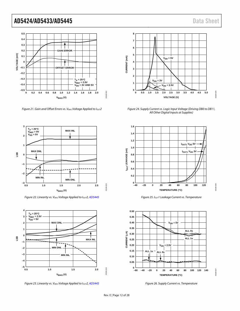
Figure 21. Gain and Offset Errors vs. VBIAS Voltage Applied to IOUT2
–3
–2
–1
0
1
2
3
LSB
0316
0-02
3
VBIAS (V)
1.00.5 1.5 2.0 2.5
MAX INL
MAX DNL
MIN INLMIN DNL
TA = 25°CVREF = 0VVDD = 5V
Figure 22. Linearity vs. VBIAS Voltage Applied to IOUT2, AD5445
–5
–4
–3
–2
–1
0
1
2
3
4
LSB
0316
0-02
4
VBIAS (V)
0.5 1.51.0 2.0
MAX INL
MAX DNL
MIN INL
MIN DNL
TA = 25°CVREF = 2.5VVDD = 5V
Figure 23. Linearity vs. VBIAS Voltage Applied to IOUT2, AD5445
0
1
2
3
4
5
CU
RR
ENT
(mA
)
6
7
8
0 0.5 1.0 1.5 2.0 2.5 3.0 3.5 4.0 4.5 5.0
VOLTAGE (V) 0316
0-02
5
VDD = 5V
VDD = 2.5V
VDD = 3V
Figure 24. Supply Current vs. Logic Input Voltage (Driving DB0 to DB11, All Other Digital Inputs at Supplies)
0
0.2
0.4
0.6
0.8
1.0
I OU
T LE
AK
AG
E (n
A)
1.2
1.4
1.6
4020–20 0–40 60 80 100 120
TEMPERATURE (°C) 0316
0-02
6
IOUT1 VDD 5V
IOUT1 VDD 3V
Figure 25. IOUT1 Leakage Current vs. Temperature
0
0.05
0.10
0.15
0.20
0.25
0.30
0.35
0.40
0.45
0.50
CU
RR
ENT
(A
)
–60 –40 –20 0 20 40 60 80 100 120 140
TEMPERATURE (°C) 0316
0-02
7
VDD = 5V
ALL 0s
ALL 1s
ALL 0sALL 1s
VDD = 2.5V
Figure 26. Supply Current vs. Temperature

Data Sheet AD5424/AD5433/AD5445
Rev. E | Page 13 of 28
0
2
4
6
8
10
12
14
I DD
(mA
)
10k1k10 1001 100k 1M 10M 100M
FREQUENCY (Hz) 0316
0-02
8
VDD = 5V
VDD = 2.5V
VDD = 3V
TA = 25°CLOADING ZS TO FS
Figure 27. Supply Current vs. Update Rate
GA
IN (d
B)
10k1k10 1001 100k 1M 10M 100M
FREQUENCY (Hz) 0316
0-02
9–102–96–90–84–78–72–66–60–54–48–42–36–30–24–18–12
–606
TA = 25°CLOADINGZS TO FS
ALL ON
ALL OFF
DB11DB10DB9DB8DB7DB6DB5DB4DB3DB2DB1DB0
TA = 25°CVDD = 5V
VREF = ±3.5VINPUT
CCOMP = 1.8pFAD8038 AMPLIFIER
AD5445 DAC
Figure 28. Reference Multiplying Bandwidth vs. Frequency and Code
–0.8
–0.6
–0.4
–0.2
0
0.2
GA
IN (d
B)
10k1k10 1001 100k 1M 10M 100M
FREQUENCY (Hz) 0316
0-03
0
TA = 25°CVDD = 5VVREF = ±3.5VCCOMP = 1.8pFAD8038 AMPLIFIERAD5445 DAC
Figure 29. Reference Multiplying Bandwidth—All 1s Loaded
GA
IN (d
B)
–9
–6
–3
0
3
0316
0-03
1
FREQUENCY (Hz)
100k10k 1M 10M 100M
TA = 25°CVDD = 5VAD5445
VREF = ±2V, AD8038 CC 1.47pFVREF = ±2V, AD8038 CC 1pFVREF = ±0.15V, AD8038 CC 1pFVREF = ±0.15V, AD8038 CC 1.47pFVREF = ±3.51V, AD8038 CC 1.8pF
Figure 30. Reference Multiplying Bandwidth vs. Frequency and Compensation Capacitor
–0.010
–0.005
0.005
0.025
0.035
0.045
0.015
0
0.020
0.030
0.040
0.010
OU
TPU
T VO
LTA
GE
(V)
0 20 40 60 80 100 120 140 160 180 200
TIME (ns) 0316
0-03
2
TA = 25°CVREF = 0VAD8038 AMPLIFIERCCOMP = 1.8pF
0x7FF TO 0x800
0x800 TO 0x7FF
VDD = 5V
VDD = 3V
VDD = 3V
VDD = 5V
Figure 31. Midscale Transition, VREF = 0 V
OU
TPU
T VO
LTA
GE
(V)
0 20 40 60 80 100 120 140 160 180 200
TIME (ns) 0316
0-03
3–1.77
–1.76
–1.75
–1.74
–1.73
–1.72
–1.71
–1.70
–1.69
–1.680x7FF TO 0x800
0x800 TO 0x7FF
VDD = 5V
VDD = 3V
VDD = 3V
VDD = 5V
TA = 25°CVREF = 3.5VAD8038 AMPLIFIERCCOMP = 1.8pF
Figure 32. Midscale Transition, VREF = 3.5 V

AD5424/AD5433/AD5445 Data Sheet
Rev. E | Page 14 of 28
0316
0-06
2
VOLTAGE (V)5.52.5 3.0 3.5 4.0 4.5 5.0
THR
ESH
OLD
VO
LTA
GE
(V)
1.8
1.4
1.6
1.0
1.2
0.4
0.6
0.8
0.2
0
TA = 25°C
VIL
VIH
Figure 33. Threshold Voltages vs. Supply Voltage
–120
–100
–80
–60
–40
–20
0
20
PSR
R (d
B)
0316
0-03
4
1 10 100 1k 10k 100k 1M 10M
FREQUENCY (Hz)
TA = 25°CVDD = 3VAMP = AD8038
FULL SCALE
ZERO SCALE
Figure 34. Power Supply Rejection vs. Frequency
–90
–85
–80
–75
–70
–65
–60
THD
+ N
(dB
)
100 1k1 10 10k 100k 1M
FREQUENCY (Hz) 0316
0-03
5
TA = 25°CVDD = 3VVREF = 3.5V p-p
Figure 35. THD and Noise vs. Frequency
0
20
40
60
80
100
SFD
R (d
B)
0 20 40 60 80 100 120 140 160 180 200
fOUT (kHz) 0316
0-03
6
TA = 25°CVREF = 3.5VAD8038 AMPLIFIERAD5445
MCLK = 1MHz
MCLK = 200kHz
MCLK = 0.5MHz
Figure 36. Wideband SFDR vs. fOUT Frequency
0
10
20
30
40
50
60
70
80
90
SFD
R (d
B)
0 100 200 300 400 500 600 700 800 900 1000
fOUT (kHz) 0316
0-03
7
MCLK = 5MHz
MCLK = 10MHz
MCLK = 25MHz
TA = 25°CVREF = 3.5VAD8038 AMPLIFIERAD5445
Figure 37. Wideband SFDR vs. fOUT Frequency
–90
–80
–70
–60
–50
–40
–30
–20
–10
0
SFD
R (d
B)
4 60 2 8 10 12
FREQUENCY (MHz) 0316
0-03
8
TA = 25°CVDD = 5VAMP = AD8038AD544565k CODES
Figure 38. Wideband SFDR, fOUT = 100 kHz, Clock = 25 MHz

Data Sheet AD5424/AD5433/AD5445
Rev. E | Page 15 of 28
–100
–90
–80
–70
–60
–50
–40
–30
–20
–10
0
SFD
R (d
B)
0 0.5 1.0 1.5 2.0 2.5 3.0 3.5 4.0 4.5 5.0
FREQUENCY (MHz) 0316
0-03
9
TA = 25°CVDD = 5VAMP = AD8038AD544565k CODES
Figure 39. Wideband SFDR, fOUT = 500 kHz, Clock = 10 MHz
–90
–80
–70
–60
–50
–40
–30
–20
–10
0
SFD
R (d
B)
0 0.5 1.0 1.5 2.0 2.5 3.0 3.5 4.0 4.5 5.0
FREQUENCY (MHz) 0316
0-04
0
TA = 25°CVDD = 5VAMP = AD8038AD544565k CODES
Figure 40. Wideband SFDR, fOUT = 50 kHz, Clock = 10 MHz
–100
–90
–80
–70
–60
–50
–40
–30
–20
–10
0
SFD
R (d
B)
250 300 350 400 450 500 550 600 650 700 750
FREQUENCY (kHz) 0316
0-04
1
TA = 25°CVDD = 3VAMP = AD8038AD544565k CODES
Figure 41. Narrow-Band Spectral Response, fOUT = 500 kHz, Clock = 25 MHz
–120
–100
–80
–60
–40
–20
0
20
SFD
R (d
B)
50 60 70 80 90 100 110 120 130 140 150
FREQUENCY (kHz) 0316
0-04
2
TA = 25°CVDD = 3VAMP = AD8038AD544565k CODES
Figure 42. Narrow-Band SFDR, fOUT = 100 kHz, MCLK = 25 MHz
–100
–90
–80
–70
–60
–50
–40
–30
–20
–10
0
(dB
)
200 250 300 350 400 450 500 550 600 650 700
FREQUENCY (kHz) 0316
0-04
3
TA = 25°CVDD = 3VAMP = AD8038AD544565k CODES
Figure 43. Narrow-Band IMD, fOUT = 400 kHz, 500 kHz, Clock = 10 MHz
–100
–90
–80
–70
–60
–50
–40
–30
–20
–10
0
(dB
)
70 75 80 85 90 95 100 105 110 115 120
FREQUENCY (kHz) 0316
0-04
4
TA = 25°CVDD = 3VAMP = AD8038AD544565k CODES
Figure 44. Narrow-Band IMD, fOUT = 90 kHz, 100 kHz, Clock = 10 MHz

AD5424/AD5433/AD5445 Data Sheet
Rev. E | Page 16 of 28
–100
–90
–80
–70
–60
–50
–40
–30
–20
–10
0
(dB
)
20 25 30 35 40 45 50 55 60 65 70
FREQUENCY (kHz) 0316
0-04
5
TA = 25°CVDD = 5VAMP = AD8038AD544565k CODES
MCLK 10MHzVDD 5V
Figure 45. Narrow-Band IMD, fOUT = 40 kHz, 50 kHz, Clock = 10 MHz
–100
–90
–80
–70
–60
–50
–40
–30
–20
–10
0
(dB
)
20015050 1000 250 300 350 400
FREQUENCY (kHz) 0316
0-04
6
TA = 25°CVDD = 5VAMP = AD8038AD544565k CODES
Figure 46. Wideband IMD, fOUT = 90 kHz, 100 kHz, Clock = 25 MHz
–100
–90
–80
–70
–60
–50
–40
–30
–20
–10
0
(dB
)
0 20 40 60 80 100 120 140 160 180 200
FREQUENCY (kHz) 0316
0-04
7
TA = 25°CVDD = 5VAMP = AD8038AD544565k CODES
Figure 47. Wideband IMD, fOUT = 60 kHz, 50 kHz, Clock = 10 MHz

Data Sheet AD5424/AD5433/AD5445
Rev. E | Page 17 of 28
TERMINOLOGY Relative Accuracy Relative accuracy or endpoint nonlinearity is a measure of the maximum deviation from a straight line passing through the endpoints of the DAC transfer function. It is measured after adjusting zero scale and full scale and is normally expressed in LSBs or as a percentage of full-scale reading.
Differential Nonlinearity Differential nonlinearity is the difference between the measured change and the ideal 1 LSB change between any two adjacent codes. A specified differential nonlinearity of –1 LSB maximum over the operating temperature range ensures monotonicity.
Gain Error Gain error or full-scale error is a measure of the output error between an ideal DAC and the actual device output. For these DACs, ideal maximum output is VREF – 1 LSB. Gain error of the DACs is adjustable to 0 with external resistance.
Output Leakage Current Output leakage current is current that flows in the DAC ladder switches when these are turned off. For the IOUT1 terminal, it can be measured by loading all 0s to the DAC and measuring the IOUT1 current. Minimum current flows in the IOUT2 line when the DAC is loaded with all 1s.
Output Capacitance Capacitance from IOUT1, or IOUT2, to AGND.
Output Current Settling Time This is the amount of time it takes for the output to settle to a specified level for a full-scale input change. For these devices, it is specified with a 100 Ω resistor to ground.
The settling time specification includes the digital delay from the CS rising edge to the full-scale output change.
Digital-to-Analog Glitch Impulse The amount of charge injected from the digital inputs to the analog output when the inputs change state. This is normally specified as the area of the glitch in either pA seconds or nV seconds, depending upon whether the glitch is measured as a current or voltage signal.
Digital Feedthrough When the device is not selected, high frequency logic activity on the device digital inputs can be capacitively coupled through the device to show up as noise on the IOUT pins and subsequently in the following circuitry. This noise is called digital feedthrough.
Multiplying Feedthrough Error This is the error due to capacitive feedthrough from the DAC reference input to the DAC IOUT1 terminal when all 0s are loaded to the DAC.
Total Harmonic Distortion (THD) The DAC is driven by an ac reference. The ratio of the rms sum of the harmonics of the DAC output to the fundamental value is the THD. Usually only the lower order harmonics are included, such as second to fifth.
( )1
25
24
23
22log20
V
VVVVTHD
+++=
Digital Intermodulation Distortion Second-order intermodulation distortion (IMD) measurements are the relative magnitude of the fa and fb tones generated digitally by the DAC and the second-order products at 2fa − fb and 2fb − fa.
Spurious-Free Dynamic Range (SFDR) SFDR is the usable dynamic range of a DAC before spurious noise interferes or distorts the fundamental signal. It is measured by the difference in amplitude between the fundamental and the largest harmonically or nonharmonically related spur from dc to full Nyquist bandwidth (half the DAC sampling rate, or fS/2). Narrow-band SFDR is a measure of SFDR over an arbitrary window size, in this case, 50% of the fundamental. Digital SFDR is a measure of the usable dynamic range of the DAC when the signal is a digitally generated sine wave.

AD5424/AD5433/AD5445 Data Sheet
Rev. E | Page 18 of 28
THEORY OF OPERATION The AD5424, AD5433, and AD5445 are 8-, 10-, and 12-bit current output DACs consisting of a standard inverting R-2R ladder configuration. A simplified diagram for the 8-bit AD5424 is shown in Figure 48. The matching feedback resistor RFB has a value of R. The value of R is typically 10 kΩ (minimum 8 kΩ and maximum 12 kΩ). If IOUT1 and IOUT2 are kept at the same potential, a constant current flows in each ladder leg, regardless of digital input code. Therefore, the input resistance presented at VREF is always constant and nominally of resistance value R. The DAC output (IOUT) is code-dependent, producing various resistances and capacitances. External amplifier choice must take into account the variation in impedance generated by the DAC on the amplifiers inverting input node.
0316
0-04
8
VREFR R R
R
2RS1 S2 S3 S8
2R 2R 2R 2R
DAC DATA LATCHESAND DRIVERS
RFBAIOUT1IOUT2
Figure 48. Simplified Ladder
Access is provided to the VREF, RFB, IOUT1, and IOUT2 terminals of the DAC, making the device extremely versatile and allowing it to be configured in several different operating modes, for example, to provide a unipolar output, 4-quadrant multiplication in bipolar mode or in single-supply modes of operation. Note that a matching switch is used in series with the internal RFB feedback resistor. If users attempt to measure RFB, power must be applied to VDD to achieve continuity.
CIRCUIT OPERATION Unipolar Mode
Using a single op amp, these devices can easily be configured to provide 2-quadrant multiplying operation or a unipolar output voltage swing, as shown in Figure 49.
When an output amplifier is connected in unipolar mode, the output voltage is given by
nREFOUTDVV2
×−=
where D is the fractional representation of the digital word loaded to the DAC and n is the resolution of the DAC.
D = 0 to 255 (8-bit AD5424) = 0 to 1023 (10-bit AD5433) = 0 to 4095 (12-bit AD5445)
Note that the output voltage polarity is opposite to the VREF polarity for dc reference voltages.
These DACs are designed to operate with either negative or positive reference voltages. The VDD power pin is only used by the internal digital logic to drive the DAC switches’ on and off states.
These DACs are also designed to accommodate ac reference input signals in the range of –10 V to +10 V.
With a fixed 10 V reference, the circuit shown in Figure 49 gives a unipolar 0 V to –10 V output voltage swing. When VIN is an ac signal, the circuit performs 2-quadrant multiplication.
Table 7 shows the relationship between digital code and expected output voltage for unipolar operation (AD5424, 8-bit device).
Table 7. Unipolar Code Table Digital Input Analog Output (V) 1111 1111 –VREF (255/256) 1000 0000 –VREF (128/256) = –VREF/2 0000 0001 VREF (1/256) 0000 0000 VREF (0/256) = 0
0316
0-04
9
VREF VREF
VDD
VDD
R/W
R1
R2
IOUT1
IOUT2
CS
RFB
GND
C1
A1
AGNDDATA
INPUTS
VOUT =0 TO –VREF
R1 AND R2 USED ONLY IF GAIN ADJUSTMENT IS REQUIRED.C1 PHASE COMPENSATION (1pF TO 2pF) MAY BE REQUIREDIF A1 IS A HIGH SPEED AMPLIFIER.
NOTES:1.2.
AD5424/AD5433/AD5445
Figure 49. Unipolar Operation

Data Sheet AD5424/AD5433/AD5445
Rev. E | Page 19 of 28
0316
0-05
0
VREF±10V
VDD
VDD
R/W
R2
R1
R320kΩ
R410kΩ
R520kΩ
IOUT1
IOUT2
CS
RFB
GND
C1
A1A2
AGNDDATAINPUTS
VOUT = –VREF TO +VREF
AD5424/AD5433/AD5445
R1 AND R2 ARE USED ONLY IF GAIN ADJUSTMENT IS REQUIRED.ADJUST R1 FOR VOUT = 0V WITH CODE 10000000 LOADED TO DAC.MATCHING AND TRACKING IS ESSENTIAL FOR RESISTOR PAIRS R3 AND R4.C1 PHASE COMPENSATION (1pF TO 2pF) MAY BE REQUIRED IF A1/A2 ISA HIGH SPEED AMPLIFIER.
NOTES:1.
2.3.
VREF
Figure 50. Bipolar Operation (4-Quadrant Multiplication)
BIPOLAR OPERATION In some applications, it can be necessary to generate full 4-quadrant multiplying operation or a bipolar output swing. This can be easily accomplished by using another external amplifier and some external resistors, as shown in Figure 50. In this circuit, the second amplifier, A2, provides a gain of 2. Biasing the external amplifier with an offset from the reference voltage, results in full 4-quadrant multiplying operation. The transfer function of this circuit shows that both negative and positive output voltages are created as the input data (D) is incremented from code zero (VOUT = –VREF) to midscale (VOUT = 0 V) to full scale (VOUT = +VREF).
( ) REFn
REFOUT VDVV −×= −12/
where D is the fractional representation of the digital word loaded to the DAC and n is the resolution of the DAC.
D = 0 to 255 (8-bit AD5424) = 0 to 1023 (10-bit AD5433) = 0 to 4095 (12-bit AD5445)
When VIN is an ac signal, the circuit performs 4-quadrant multiplication.
Table 8 shows the relationship between digital code and the expected output voltage for bipolar operation (AD5424, 8-bit device).
Table 8. Bipolar Code Table Digital Input Analog Output (V) 1111 1111 +VREF (127/128) 1000 0000 0 0000 0001 –VREF (127/128) 0000 0000 –VREF (128/128)
Stability
In the I-to-V configuration, the IOUT of the DAC and the inverting node of the op amp must be connected as closely as possible and proper PCB layout techniques must be employed. Since every code change corresponds to a step function, gain peaking can occur if the op amp has limited GBP and there is excessive parasitic capacitance at the inverting node. This parasitic capacitance introduces a pole into the open-loop response, which can cause ringing or instability in closed-loop applications.
An optional compensation capacitor, C1, can be added in parallel with RFB for stability, as shown in Figure 49 and Figure 50. Too small a value of C1 can produce ringing at the output, while too large a value can adversely affect the settling time. C1 must be found empirically, but 1 pF to 2 pF is generally adequate for compensation.

AD5424/AD5433/AD5445 Data Sheet
Rev. E | Page 20 of 28
SINGLE-SUPPLY APPLICATIONS Current Mode Operation
The current mode circuit in Figure 51 shows a typical circuit for operation with a single 2.5 V to 5 V supply. IOUT2 and therefore IOUT1 is biased positive by the amount applied to VBIAS. In this configuration, the output voltage is given by
VOUT = [D × (RFB/RDAC) × (VBIAS − VIN)] + VBIAS
As D varies from 0 to 255 (AD5424), 0 to 1023 (AD5433), or 0 to 4095 (AD5445), the output voltage varies from
VOUT = VBIAS to VOUT = 2VBIAS − VIN
VBIAS must be a low impedance source capable of sinking and sourcing all possible variations in current at the IOUT2 terminal.
0316
0-05
1ADDITIONAL PINS OMITTED FOR CLARITYC1 PHASE COMPENSATION (1pF TO 2pF) MAY BE REQUIREDIF A1 IS A HIGH SPEED AMPLIFIER.
NOTES:1.2.
VDD
VDD
VIN VREF
GND
DAC
C1
A1
RFB
IOUT1
IOUT2
VBIAS
VOUT
Figure 51. Single-Supply Current Mode Operation
It is important to note that VIN is limited to low voltages because the switches in the DAC ladder no longer have the same source-drain drive voltage. As a result, there on resistance differs and the linearity of the DAC degrades.
Voltage Switching Mode of Operation
Figure 52 shows these DACs operating in the voltage-switching mode. The reference voltage, VIN, is applied to the IOUT1 pin, IOUT2 is connected to AGND, and the output voltage is available at the VREF terminal. In this configuration, a positive reference voltage results in a positive output voltage, making single-supply operation possible. The output from the DAC is a voltage at a constant impedance (the DAC ladder resistance), thus an op amp is necessary to buffer the output voltage. The reference input no longer sees a constant input impedance, but one that varies with code. Therefore, the voltage input must be driven from a low impedance source.
0316
0-05
2
VIN
VDD
VDD
VREFVOUT
GND
DAC
RFB
IOUT1
IOUT2
R1
A1
R2
ADDITIONAL PINS OMITTED FOR CLARITYC1 PHASE COMPENSATION (1pF TO 2pF) MAY BE REQUIREDIF A1 IS A HIGH SPEED AMPLIFIER.
NOTES:1.2.
Figure 52. Single-Supply Voltage-Switching Mode Operation
It is important to note that VIN is limited to low voltages because the switches in the DAC ladder no longer have the same source-drain drive voltage. As a result, there on resistance differs, which degrades the linearity of the DAC. See Figure 18 to Figure 23. Also, VIN must not go negative by more than 0.3 V; otherwise, an internal diode turns on, exceeding the maximum ratings of the device. In this type of application, the full range of multiplying capability of the DAC is lost.

Data Sheet AD5424/AD5433/AD5445
Rev. E | Page 21 of 28
ADDING GAIN In applications where the output voltage is required to be greater than VIN, gain can be added with an additional external amplifier or it can be achieved in a single stage. It is important to consider the effect of the temperature coefficients of the thin film resistors of the DAC. Simply placing a resistor in series with the RFB resistor causes mismatches in the temperature coefficients and results in larger gain temperature coefficient errors. Instead, the circuit shown in Figure 53 is a recommended method of increasing the gain of the circuit. R1, R2, and R3 must have similar temperature coefficients, but they need not match the temperature coefficients of the DAC. This approach is recommended in circuits where gains greater than 1 are required. Note that RFB >> R2||R3 and take into consideration a gain error percentage of 100 × (R2||R3)/RFB.
0316
0-05
4
8-/10-/12-BITDAC
GND
VDD RFB
VDD
VOUTVREF
VIN
ADDITIONAL PINS OMITTED FOR CLARITYC1 PHASE COMPENSATION (1pF TO 2pF) MAY BEREQUIRED IF A1 IS A HIGH SPEED AMPLIFIER.
NOTES:1.2.
C1
R1 IOUT1
IOUT2
R1 =
GAIN = R2 + R3R2
R3
R2
R2R3R2 + R3
Figure 53. Increasing the Gain of the Current Output DAC
DACS USED AS A DIVIDER OR PROGRAMMABLE GAIN ELEMENT Current steering DACs are very flexible and lend themselves to many different applications. If this type of DAC is connected as the feedback element of an op amp and RFB is used as the input resistor, as shown in Figure 54, then the output voltage is inversely proportional to the digital input fraction, D.
For D = 1 – 2–n the output voltage is
VOUT = –VIN/D = –VIN/(1 − 2–n)
As D is reduced, the output voltage increases. For small values of D, it is important to ensure that the amplifier does not saturate and that the required accuracy is met.
For example, in the circuit shown in Figure 54, an 8-bit DAC driven with the binary code 0x10 (00010000), that is, 16 decimal, must cause the output voltage to be 16 × VIN. However, if the DAC has a linearity specification of ±0.5 LSB, then D can in fact have a weight anywhere in the range 15.5/256 to 16.5/256 so that the possible output voltage falls in the range 15.5 VIN to 16.5 VIN—an error of 3% even though the DAC itself has a maximum error of 0.2%.
0316
0-05
5
GND
RFB
VDD
VDD
VOUT
VREF
VIN
NOTE:ADDITIONAL PINS OMITTED FOR CLARITY
IOUT1
IOUT2
Figure 54. Current-Steering DAC Used as a Divider or
Programmable Gain Element
DAC leakage current is also a potential error source in divider circuits. The leakage current must be counterbalanced by an opposite current supplied from the op amp through the DAC. Since only a fraction, D, of the current into the VREF terminal is routed to the IOUT1 terminal, the output voltage has to change as follows:
Output Error Voltage due to DAC Leakage = (Leakage × R)/D
where R is the DAC resistance at the VREF terminal.
For a DAC leakage current of 10 nA, R = 10 kΩ, and a gain (that is, 1/D) of 16, the error voltage is 1.6 mV.

AD5424/AD5433/AD5445 Data Sheet
Rev. E | Page 22 of 28
Table 9. Suitable ADI Precision References Device No. Output Voltage (V) Initial Tolerance (%) Temp Drift (ppm/°C) ISS (mA) Output Noise (µV p-p) Package ADR01 10 0.05 3 1 20 SOIC ADR01 10 0.05 9 1 20 TSOT-23, SC70 ADR02 5 0.06 3 1 10 SOIC ADR02 5 0.06 9 1 10 TSOT-23, SC70 ADR03 2.5 0.10 3 1 6 SOIC ADR03 2.5 0.10 9 1 6 TSOT-23, SC70 ADR06 3 0.10 3 1 10 SOIC ADR06 3 0.10 9 1 10 TSOT-23, SC70 ADR431 2.5 0.04 3 0.8 3.5 SOIC ADR435 5 0.04 3 0.8 8 SOIC ADR391 2.5 0.16 9 0.12 5 TSOT-23 ADR395 5 0.10 9 0.12 8 TSOT-23
Table 10. Suitable ADI Precision Op Amps
Device No. Supply Voltage (V) VOS (Max) (µV) IB (Max) (nA) 0.1 Hz to 10 Hz Noise (µV p-p) Supply Current (µA) Package
OP97 ±2 to ±20 25 0.1 0.5 600 SOIC OP1177 ±2.5 to ±15 60 2 0.4 500 MSOP, SOIC AD8551 2.7 to 5 5 0.05 1 975 MSOP, SOIC AD8603 1.8 to 6 50 0.001 2.3 50 TSOT AD8628 2.7 to 6 5 0.1 0.5 850 TSOT, SOIC
Table 11. Suitable ADI High Speed Op Amps Device No. Supply Voltage (V) BW at ACL (MHz) Slew Rate (V/µs) VOS (Max) (µV) IB (Max) (nA) Package AD8065 5 to 24 145 180 1500 6000 SOIC, SOT-23, MSOP AD8021 ±2.5 to ±12 490 120 1000 10500 SOIC, MSOP AD8038 3 to 12 350 425 3000 750 SOIC, SC70-5 AD9631 ±3 to ±6 320 1300 10000 7000 SOIC
REFERENCE SELECTION When selecting a reference for use with the AD5424/AD5433/ AD5445 family of current output DACs, pay attention to the output voltage temperature coefficient specification of the reference. This parameter not only affects the full-scale error, but can also affect the linearity (INL and DNL) performance. The reference temperature coefficient must be consistent with the system accuracy specifications. For example, an 8-bit system required to hold its overall specification to within 1 LSB over the temperature range 0°C to 50°C dictates that the maximum system drift with temperature must be less than 78 ppm/°C.
A 12-bit system with the same temperature range to overall specification within 2 LSBs requires a maximum drift of 10 ppm/°C. By choosing a precision reference with low output temperature coefficient this error source can be minimized. Table 9 suggests some references available from Analog Devices that are suitable for use with this range of current output DACs.
AMPLIFIER SELECTION The primary requirement for the current-steering mode is an amplifier with low input bias currents and low input offset voltage. The input offset voltage of an op amp is multiplied by the variable gain (due to the code dependent output resistance of the DAC) of the circuit. A change in the noise gain between two adjacent digital fractions produces a step change in the output voltage due to the amplifier’s input offset voltage. This output voltage change is superimposed on the desired change in output between the two codes and gives rise to a differential linearity error, which, if large enough, can cause the DAC to be non-monotonic. In general, the input offset voltage must be <1/4 LSB to ensure monotonic behavior when stepping through codes.
The input bias current of an op amp also generates an offset at the voltage output as a result of the bias current flowing into the feedback resistor, RFB. Most op amps have input bias currents low enough to prevent significant errors in 12-bit applications.
Common-mode rejection of the op amp is important in voltage-switching circuits, since it produces a code dependent error at the voltage output of the circuit. Most op amps have adequate common mode rejection for use at 8-, 10-, and 12-bit resolution.

Data Sheet AD5424/AD5433/AD5445
Rev. E | Page 23 of 28
Provided the DAC switches are driven from true wideband low impedance sources (VIN and AGND), they settle quickly. Consequently, the slew rate and settling time of a voltage switching DAC circuit is determined largely by the output op amp. To obtain minimum settling time in this configuration, it is important to minimize capacitance at the VREF node (voltage output node in this application) of the DAC. This is done by using low inputs capacitance buffer amplifiers and careful board design.
Most single-supply circuits include ground as part of the analog signal range, which in turns requires an amplifier that can handle rail-to-rail signals. There is a large range of single-supply amplifiers available from Analog Devices.
PARALLEL INTERFACE Data is loaded to the AD5424/AD5433/AD5445 in the format of an 8-, 10-, or 12-bit parallel word. Control lines CS and R/W allow data to be written to or read from the DAC register. A write event takes place when CS and R/W are brought low, data available on the data lines fills the shift register, and the rising edge of CS latches the data and transfers the latched data-word to the DAC register. The DAC latches are not transparent, thus a write sequence must consist of a falling and rising edge on CSto ensure that data is loaded to the DAC register and its analog equivalent is reflected on the DAC output.
A read event takes place when R/W is held high and CS is brought low. New data is loaded from the DAC register back to the input register and out onto the data line where it can be read back to the controller for verification or diagnostic purposes.
MICROPROCESSOR INTERFACING ADSP-2191M-to-AD5424/AD5433/AD5445 Interface
Figure 55 shows the AD5424/AD5433/AD5445 interfaced to the ADSP-2191M as a memory-mapped device. A single wait state can be necessary to interface the AD5424/AD5433/ AD5445 to the ADSP-2191M, depending on the clock speed of the DSP. The wait state can be programmed via the data memory wait state control register of the ADSP-2191M (see the ADSP 21xx Processors: Manuals for details).
0316
0-05
6
R/W
DB0 TO DB11
AD5424/AD5433/AD5445*
ADDRESSDECODER CS
DATA 0 TODATA 23
ADDRESS BUSADDR0 TOADRR13
ADSP-2191M*
DATA BUS
DMS
WR
*ADDITIONAL PINS OMITTED FOR CLARITY Figure 55. ADSP-2191M-to-AD5424/AD5433/AD5445 Interface
8xC51-to-AD5424/AD5433/AD5445 Interface
Figure 56 shows the interface between the AD5424/AD5433/ AD5445 and the 8xC51 family of DSPs. To facilitate external data memory access, the address latch enable (ALE) mode is enabled. The low byte of the address is latched with this output pulse during access to external memory. AD0 to AD7 are the multiplexed low order addresses and data bus and require strong internal pull-ups when emitting 1s. During access to external memory, A8 to A15 are the high order address bytes. Since these ports are open drained, they also require strong internal pull-ups when emitting 1s.
0316
0-06
3
R/W
DB0 TO DB11
AD5424/AD5433/AD5445*
ADDRESSDECODER CS
AD0 TO AD7
ADDRESS BUSA8 TO A15
8051*
DATA BUS
WR
*ADDITIONAL PINS OMITTED FOR CLARITY
8-BITLATCHALE
Figure 56. 8xC51-to-AD5424/AD5433/AD5445 Interface
Blackfin Processor-to-AD5424/AD5433/AD5445 Interface
Figure 57 shows a typical interface between the AD5424/ AD5433/AD5445 and the Blackfin processor family of DSPs. The asynchronous memory write cycle of the processor drives the digital inputs of the DAC. The AMSx line is actually four memory select lines. Internal ADDR lines are decoded into AMS3-0, these lines are then inserted as chip selects. The rest of the interface is a standard handshaking operation.
0316
0-05
7
R/W
DB0 TO DB11
AD5424/AD5433/AD5445*
ADDRESSDECODER CS
DATA 0 TODATA 23
ADDRESS BUSADDR1 TOADRR19
BLACKFINPROCESSOR
DATA BUS
AMSx
AWE
*ADDITIONAL PINS OMITTED FOR CLARITY Figure 57. Blackfin Processor-to-AD5424/AD5433/AD5445 Interface

AD5424/AD5433/AD5445 Data Sheet
Rev. E | Page 24 of 28
PCB LAYOUT AND POWER SUPPLY DECOUPLING In any circuit where accuracy is important, careful consideration of the power supply and ground return layout helps to ensure the rated performance. Design the printed circuit board on which the AD5424/AD5433/AD5445 is mounted so that the analog and digital sections are separated and confined to certain areas of the board. If the DAC is in a system where multiple devices require an AGND-to-DGND connection, make the connection at one point only. Establish the star ground point as close as possible to the device.
These DACs must have ample supply bypassing of 10 µF in parallel with 0.1 µF on the supply, located as close to the package as possible and ideally right up against the device. The 0.1 µF capacitor must have low effective series resistance (ESR) and effective series inductance (ESI), like the common ceramic types that provide a low impedance path to ground at high frequencies, to handle transient currents due to internal logic switching. Low ESR 1 µF to 10 µF tantalum or electrolytic capacitors must also be applied at the supplies to minimize transient disturbance and filter out low frequency ripple.
Shield fast switching signals such as clocks with digital ground to avoid radiating noise to other parts of the board and must never be run near the reference inputs.
Avoid crossover of digital and analog signals. Running traces on opposite sides of the board at right angles to each other reduces the effects of feedthrough through the board. A microstrip technique is by far the best, but not always possible with a double-sided board. In this technique, the component side of the board is dedicated to the ground plane, while signal traces are placed on the solder side.
It is good practice to employ compact, minimum lead length PCB layout design. Ensure that leads to the input are as short as possible to minimize IR drops and stray inductance.
Match the PCB metal traces between VREF and RFB to minimize gain error. To maximize high frequency performance, locate the I-to-V amplifier as close to the device as possible.
Table 12. Overview of the AD5424/AD5433/AD5445 and Related Multiplying DACs Part No. Resolution No. DACs INL(LSB) Interface Package Features AD5424 8 1 ±0.25 Parallel RU-16, CP-20 10 MHz BW, 17 ns CS pulse width
AD5426 8 1 ±0.25 Serial RM-10 10 MHz BW, 50 MHz serial AD5428 8 2 ±0.25 Parallel RU-20 10 MHz BW, 17 ns CS pulse width
AD5429 8 2 ±0.25 Serial RU-10 10 MHz BW, 50 MHz serial AD5450 8 1 ±0.25 Serial RJ-8 10 MHz BW, 50 MHz serial AD5432 10 1 ±0.5 Serial RM-10 10 MHz BW, 50 MHz serial AD5433 10 1 ±0.5 Parallel RU-20, CP-20 10 MHz BW, 17 ns CS pulse width
AD5439 10 2 ±0.5 Serial RU-16 10 MHz BW, 50 MHz serial AD5440 10 2 ±0.5 Parallel RU-24 10 MHz BW, 17 ns CS pulse width
AD5451 10 1 ±0.25 Serial RJ-8 10 MHz BW, 50 MHz serial AD5443 12 1 ±1 Serial RM-10 10 MHz BW, 50 MHz serial AD5444 12 1 ±0.5 Serial RM-8 50 MHz serial interface AD5415 12 2 ±1 Serial RU-24 10 MHz BW, 50 MHz serial AD5405 12 2 ±1 Parallel CP-40 10 MHz BW, 17 ns CS pulse width
AD5445 12 2 ±1 Parallel RU-20, CP-20 10 MHz BW, 17 ns CS pulse width
AD5447 12 2 ±1 Parallel RU-24 10 MHz BW, 17 ns CS pulse width
AD5449 12 2 ±1 Serial RU-16 10 MHz BW, 50 MHz serial AD5452 12 1 ±0.5 Serial RJ-8, RM-8 10 MHz BW, 50 MHz serial AD5446 14 1 ±1 Serial RM-8 10 MHz BW, 50 MHz serial AD5453 14 1 ±2 Serial UJ-8, RM-8 10 MHz BW, 50 MHz serial AD5553 14 1 ±1 Serial RM-8 4 MHz BW, 50 MHz serial clock AD5556 14 1 ±1 Parallel RU-28 4 MHz BW, 20 ns WR pulse width
AD5555 14 2 ±1 Serial RM-8 4 MHz BW, 50 MHz serial clock AD5557 14 2 ±1 Parallel RU-38 4 MHz BW, 20 ns WR pulse width
AD5543 16 1 ±2 Serial RM-8 4 MHz BW, 50 MHz serial clock AD5546 16 1 ±2 Parallel RU-28 4 MHz BW, 20 ns WR pulse width
AD5545 16 2 ±2 Serial RU-16 4 MHz BW, 50 MHz serial clock AD5547 16 2 ±2 Parallel RU-38 4 MHz BW, 20 ns WR pulse width

Data Sheet AD5424/AD5433/AD5445
Rev. E | Page 25 of 28
OUTLINE DIMENSIONS
16 9
81
PIN 1
SEATINGPLANE
8°0°
4.504.404.30
6.40BSC
5.105.004.90
0.65BSC
0.150.05
1.20MAX
0.200.09 0.75
0.600.45
0.300.19
COPLANARITY0.10
COMPLIANT TO JEDEC STANDARDS MO-153-AB Figure 58. 16-Lead Thin Shrink Small Outline Package [TSSOP]
(RU-16) Dimensions shown in millimeters
COMPLIANT TO JEDEC STANDARDS MO-153-AC
20
1
11
106.40 BSC
4.504.404.30
PIN 1
6.606.506.40
SEATINGPLANE
0.150.05
0.300.19
0.65BSC
1.20 MAX 0.200.09 0.75
0.600.45
8°0°COPLANARITY
0.10
Figure 59. 20-Lead Thin Shrink Small Outline Package [TSSOP]
(RU-20) Dimensions shown in millimeters

AD5424/AD5433/AD5445 Data Sheet
Rev. E | Page 26 of 28
0.50BSC
0.650.600.55
0.300.250.18
COMPLIANT TO JEDEC STANDARDS MO-220-WGGD-1.
BOTTOM VIEWTOP VIEW
EXPOSEDPAD
PIN 1INDICATOR
4.104.00 SQ3.90
SEATINGPLANE
0.800.750.70 0.05 MAX
0.02 NOM
0.20 REF
0.20 MIN
COPLANARITY0.08
PIN 1INDICATOR
2.302.10 SQ2.00
FOR PROPER CONNECTION OFTHE EXPOSED PAD, REFER TOTHE PIN CONFIGURATION ANDFUNCTION DESCRIPTIONSSECTION OF THIS DATA SHEET.
120
61011
1516
5
08-1
6-20
10-B
Figure 60. 20-Lead Lead Frame Chip Scale Package [LFCSP_WQ]
4 mm × 4 mm Body, Very Thin Quad (CP-20-6)
Dimensions shown in millimeters
ORDERING GUIDE Model1 Resolution (Bits) INL (LSB) Temperature Range Package Description Package Option AD5424YRU 8 ±0.25 −40°C to +125°C 16-Lead TSSOP RU-16 AD5424YRUZ 8 ±0.25 –40°C to +125°C 16-Lead TSSOP RU-16 AD5424YRUZ-REEL 8 ±0.25 –40°C to +125°C 16-Lead TSSOP RU-16 AD5424YRUZ-REEL7 8 ±0.25 –40°C to +125°C 16-Lead TSSOP RU-16 AD5424YCPZ 8 ±0.25 –40°C to +125°C 20-Lead LFCSP_WQ CP-20-6 AD5424YCPZ-REEL7 8 ±0.25 –40°C to +125°C 20-Lead LFCSP_WQ CP-20-6 AD5433YRU 10 ±0.5 –40°C to +125°C 20-Lead TSSOP RU-20 AD5433YRUZ 10 ±0.5 –40°C to +125°C 20-Lead TSSOP RU-20 AD5433YRUZ-REEL 10 ±0.5 –40°C to +125°C 20-Lead TSSOP RU-20 AD5433YRUZ-REEL7 10 ±0.5 –40°C to +125°C 20-Lead TSSOP RU-20 AD5433YCPZ 10 ±0.5 –40°C to +125°C 20-Lead LFCSP_WQ CP-20-6 AD5445YRU 12 ±1 –40°C to +125°C 20-Lead TSSOP RU-20 AD5445YRUZ 12 ±1 –40°C to +125°C 20-Lead TSSOP RU-20 AD5445YRUZ-REEL 12 ±1 –40°C to +125°C 20-Lead TSSOP RU-20 AD5445YRUZ-REEL7 12 ±1 –40°C to +125°C 20-Lead TSSOP RU-20 AD5445YCPZ 12 ±1 –40°C to +125°C 20-Lead LFCSP_WQ CP-20-6 EVAL-AD5445SDZ Evaluation Board 1 Z = RoHS Compliant Part.

Data Sheet AD5424/AD5433/AD5445
Rev. E | Page 27 of 28
NOTES

AD5424/AD5433/AD5445 Data Sheet
Rev. E | Page 28 of 28
NOTES
©2003–2016 Analog Devices, Inc. All rights reserved. Trademarks and registered trademarks are the property of their respective owners. D03160-0-1/16(E)