Embed Size (px)
Citation preview
8-bit Microcontroller with 16/32/64K Bytes In-SystemProgrammable Flash
ATmega164PATmega324PATmega644P
Automotive
Summary
7674DS–AVR–08/08
Features• High-performance, Low-power AVR® 8-bit Microcontroller• Advanced RISC Architecture
– 131 Powerful Instructions – Most Single-clock Cycle Execution– 32 x 8 General Purpose Working Registers– Fully Static Operation– Up to 16 MIPS Throughput at 16 MHz– On-chip 2-cycle Multiplier
• Nonvolatile Program and Data Memories– 16/32/64K Bytes of In-System Self-Programmable Flash
Endurance: 10,000 Write/Erase Cycles– Optional Boot Code Section with Independent Lock Bits
In-System Programming by On-chip Boot ProgramTrue Read-While-Write Operation
– 512B/1K/2K Bytes EEPROMEndurance: 100,000 Write/Erase Cycles
– 1/2/4K Bytes Internal SRAM– Programming Lock for Software Security
• JTAG (IEEE std. 1149.1 Compliant) Interface– Boundary-scan Capabilities According to the JTAG Standard– Extensive On-chip Debug Support– Programming of Flash, EEPROM, Fuses, and Lock Bits through the JTAG Interface
• Peripheral Features– Two 8-bit Timer/Counters with Separate Prescalers and Compare Modes– One 16-bit Timer/Counter with Separate Prescaler, Compare Mode, and Capture
Mode– Real Time Counter with Separate Oscillator– Six PWM Channels– 8-channel, 10-bit ADC
Differential mode with selectable gain at 1x, 10x or 200x(1)
– Byte-oriented Two-wire Serial Interface– Two Programmable Serial USART– Master/Slave SPI Serial Interface– Programmable Watchdog Timer with Separate On-chip Oscillator– On-chip Analog Comparator– Interrupt and Wake-up on Pin Change
• Special Microcontroller Features– Power-on Reset and Programmable Brown-out Detection– Internal Calibrated RC Oscillator– External and Internal Interrupt Sources– Six Sleep Modes: Idle, ADC Noise Reduction, Power-save, Power-down, Standby
and Extended Standby• I/O and Packages
– 32 Programmable I/O Lines– 44-lead TQFP, and 44-pad QFN/MLF
• Operating Voltages– 2.7 - 5.5V for ATmega164P/324P/644P
• Speed Grades– ATmega164P/324P/644P: 0 - 8MHz @ 2.7 - 5.5V, 0 - 16MHz @ 4.5 - 5.5V
• Power Consumption at 8 MHz, 5V, 25⋅C for ATmega644P– Active mode: 8 mA– Idle mode: 2.4 mA– Power-down Mode: 0.8 µA
Notes: 1. Differential Mode is not recommended above 85°C.
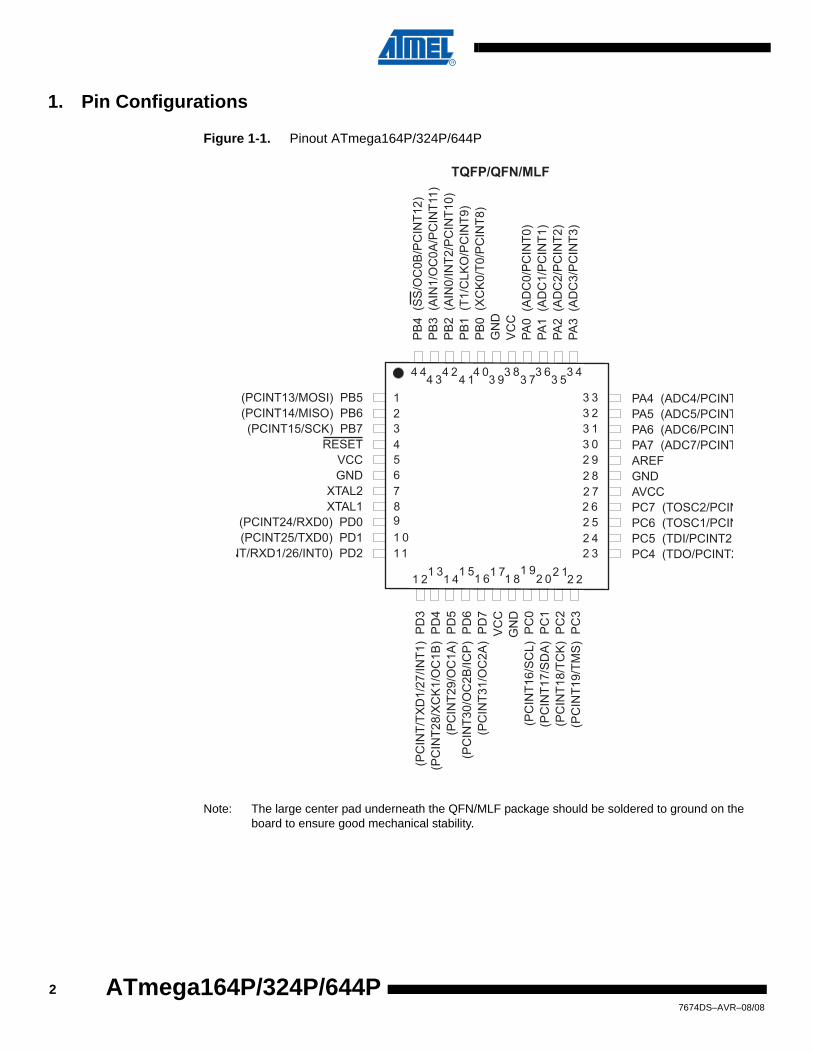
1. Pin Configurations
Figure 1-1. Pinout ATmega164P/324P/644P
Note: The large center pad underneath the QFN/MLF package should be soldered to ground on the board to ensure good mechanical stability.
PA4 (ADC4/PCINT
PA5 (ADC5/PCINT
PA6 (ADC6/PCINT
PA7 (ADC7/PCINT
AREF
GND
AVCC
PC7 (TOSC2/PCIN
PC6 (TOSC1/PCIN
PC5 (TDI/PCINT2
PC4 (TDO/PCINT2
(PCINT13/MOSI) PB5
(PCINT14/MISO) PB6
(PCINT15/SCK) PB7
RESET
VCC
GND
XTAL2
XTAL1
(PCINT24/RXD0) PD0
(PCINT25/TXD0) PD1
NT/RXD1/26/INT0) PD2
(PC
INT
/TX
D1/2
7/IN
T1)
PD
3
(PC
INT
28/X
CK
1/O
C1B
) P
D4
(PC
INT
29/O
C1A
) P
D5
(PC
INT
30/O
C2B
/IC
P)
PD
6
(PC
INT
31/O
C2A
) P
D7
VC
C
GN
D
(PC
INT
16/S
CL)
PC
0
(PC
INT
17/S
DA
) P
C1
(PC
INT
18/T
CK
) P
C2
(PC
INT
19/T
MS
) P
C3
PB
4 (S
S/O
C0B
/PC
INT
12)
PB
3 (A
IN1/O
C0A
/PC
INT
11)
PB
2 (A
IN0/IN
T2/P
CIN
T10)
PB
1 (T
1/C
LK
O/P
CIN
T9)
PB
0 (X
CK
0/T
0/P
CIN
T8)
GN
D
VC
C
PA
0 (A
DC
0/P
CIN
T0)
PA
1 (A
DC
1/P
CIN
T1)
PA
2 (A
DC
2/P
CIN
T2)
PA
3 (A
DC
3/P
CIN
T3)
TQFP/QFN/MLF
27674DS–AVR–08/08
ATmega164P/324P/644P
ATmega164P/324P/644P
2. Overview
The ATmega164P/324P/644P is a low-power CMOS 8-bit microcontroller based on the AVRenhanced RISC architecture. By executing powerful instructions in a single clock cycle, theATmega164P/324P/644P achieves throughputs approaching 1 MIPS per MHz allowing the sys-tem designer to optimize power consumption versus processing speed.
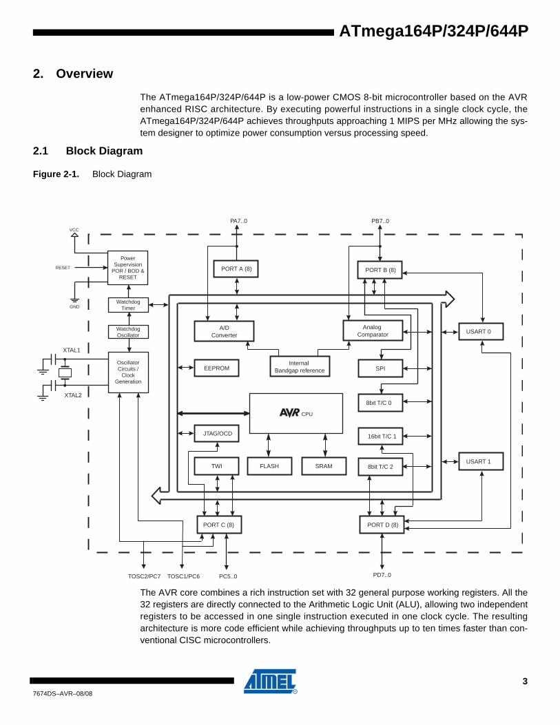
2.1 Block Diagram
Figure 2-1. Block Diagram
The AVR core combines a rich instruction set with 32 general purpose working registers. All the32 registers are directly connected to the Arithmetic Logic Unit (ALU), allowing two independentregisters to be accessed in one single instruction executed in one clock cycle. The resultingarchitecture is more code efficient while achieving throughputs up to ten times faster than con-ventional CISC microcontrollers.
CPU
GND
VCC
RESET
PowerSupervision
POR / BOD &RESET
WatchdogOscillator
WatchdogTimer
OscillatorCircuits /
ClockGeneration
XTAL1
XTAL2
PORT A (8)
PORT D (8)
PD7..0
PORT C (8)
PC5..0
TWI
SPIEEPROM
JTAG/OCD 16bit T/C 1
8bit T/C 2
8bit T/C 0
SRAMFLASH
USART 0
Internal Bandgap reference
Analog Comparator
A/DConverter
PA7..0
PORT B (8)
PB7..0
USART 1
TOSC1/PC6TOSC2/PC7
37674DS–AVR–08/08
The ATmega164P/324P/644P provides the following features: 16/32/64K bytes of In-SystemProgrammable Flash with Read-While-Write capabilities, 512B/1K/2K bytes EEPROM, 1/2/4Kbytes SRAM, 32 general purpose I/O lines, 32 general purpose working registers, Real TimeCounter (RTC), three flexible Timer/Counters with compare modes and PWM, 2 USARTs, a byteoriented 2-wire Serial Interface, a 8-channel, 10-bit ADC with optional differential input stagewith programmable gain, programmable Watchdog Timer with Internal Oscillator, an SPI serialport, IEEE std. 1149.1 compliant JTAG test interface, also used for accessing the On-chipDebug system and programming and six software selectable power saving modes. The Idlemode stops the CPU while allowing the SRAM, Timer/Counters, SPI port, and interrupt systemto continue functioning. The Power-down mode saves the register contents but freezes theOscillator, disabling all other chip functions until the next interrupt or Hardware Reset. In Power-save mode, the asynchronous timer continues to run, allowing the user to maintain a timer basewhile the rest of the device is sleeping. The ADC Noise Reduction mode stops the CPU and allI/O modules except Asynchronous Timer and ADC, to minimize switching noise during ADCconversions. In Standby mode, the Crystal/Resonator Oscillator is running while the rest of thedevice is sleeping. This allows very fast start-up combined with low power consumption. InExtended Standby mode, both the main Oscillator and the Asynchronous Timer continue to run.
The device is manufactured using Atmel’s high-density nonvolatile memory technology. The On-chip ISP Flash allows the program memory to be reprogrammed in-system through an SPI serialinterface, by a conventional nonvolatile memory programmer, or by an On-chip Boot programrunning on the AVR core. The boot program can use any interface to download the applicationprogram in the application Flash memory. Software in the Boot Flash section will continue to runwhile the Application Flash section is updated, providing true Read-While-Write operation. Bycombining an 8-bit RISC CPU with In-System Self-Programmable Flash on a monolithic chip,the Atmel ATmega164P/324P/644P is a powerful microcontroller that provides a highly flexibleand cost effective solution to many embedded control applications.
The ATmega164P/324P/644P AVR is supported with a full suite of program and system devel-opment tools including: C compilers, macro assemblers, program debugger/simulators, in-circuitemulators, and evaluation kits.
2.2 Comparison Between ATmega164P, ATmega324P and ATmega644P
Automotive Quality Grade
The ATmega164P/324P/644P have been developed and manufactured according to the moststringent requirements of the international standard ISO-TS-16949. This data sheet containslimit values extracted from the results of extensive characterization (Temperature and Voltage).The quality and reliability of the ATmega164P/324P/644P have been verified during regularproduct qualification as per AEC-Q100 grade 1.
Table 2-1. Differences between ATmega164P and ATmega644P
Device Flash EEPROM RAM
ATmega164P 16 Kbyte 512 Bytes 1 Kbyte
ATmega324P 32 Kbyte 1 Kbyte 2 Kbyte
ATmega644P 64 Kbyte 2 Kbyte 4 Kbyte
47674DS–AVR–08/08
ATmega164P/324P/644P
ATmega164P/324P/644P
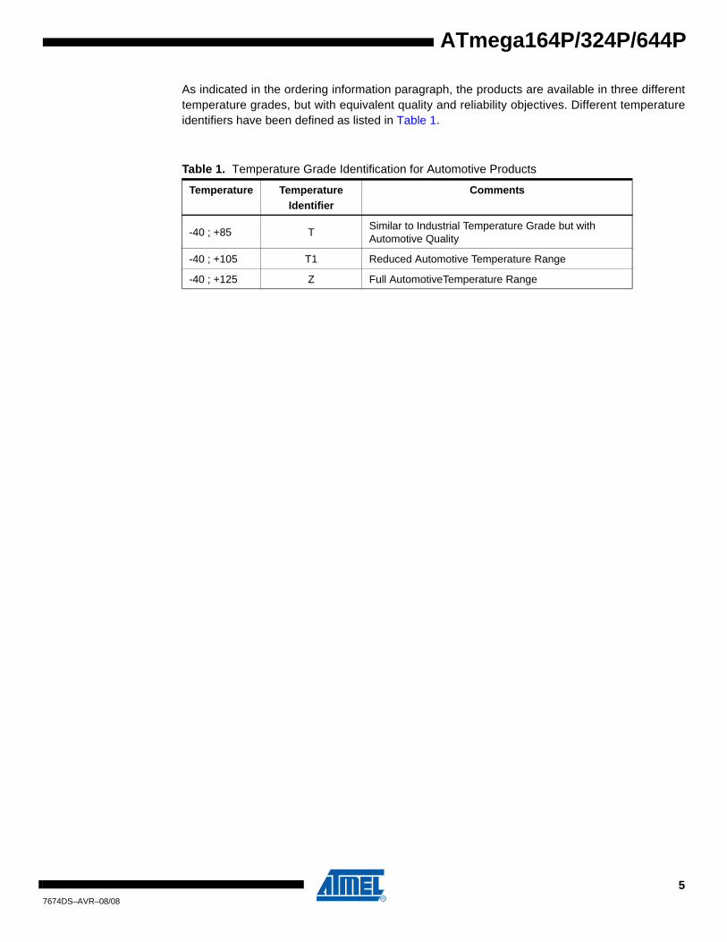
As indicated in the ordering information paragraph, the products are available in three differenttemperature grades, but with equivalent quality and reliability objectives. Different temperatureidentifiers have been defined as listed in Table 1.
Table 1. Temperature Grade Identification for Automotive Products
Temperature TemperatureIdentifier
Comments
-40 ; +85 T Similar to Industrial Temperature Grade but with Automotive Quality
-40 ; +105 T1 Reduced Automotive Temperature Range
-40 ; +125 Z Full AutomotiveTemperature Range
57674DS–AVR–08/08
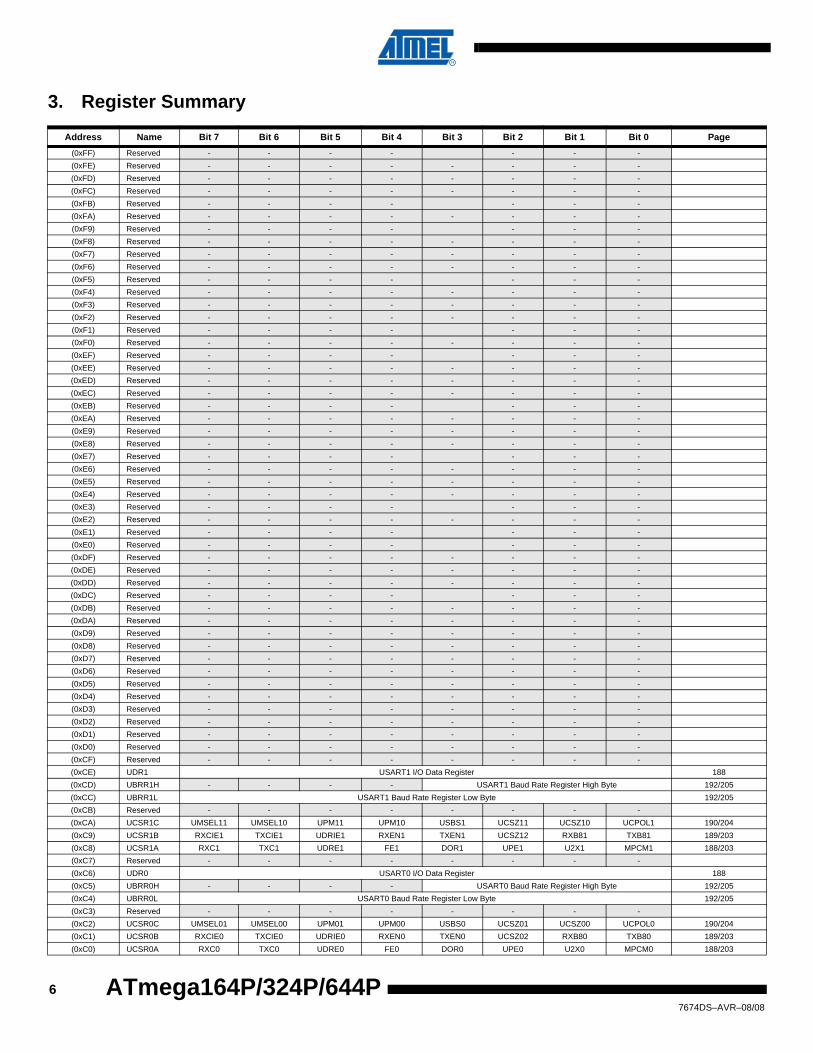
3. Register Summary
Address Name Bit 7 Bit 6 Bit 5 Bit 4 Bit 3 Bit 2 Bit 1 Bit 0 Page(0xFF) Reserved - - - - - - -(0xFE) Reserved - - - - - - - -(0xFD) Reserved - - - - - - - -(0xFC) Reserved - - - - - - - -(0xFB) Reserved - - - - - - -(0xFA) Reserved - - - - - - - -(0xF9) Reserved - - - - - - -(0xF8) Reserved - - - - - - - -(0xF7) Reserved - - - - - - - -(0xF6) Reserved - - - - - - - -(0xF5) Reserved - - - - - - -(0xF4) Reserved - - - - - - - -(0xF3) Reserved - - - - - - - -(0xF2) Reserved - - - - - - - -(0xF1) Reserved - - - - - - -(0xF0) Reserved - - - - - - - -(0xEF) Reserved - - - - - - -(0xEE) Reserved - - - - - - - -(0xED) Reserved - - - - - - - -(0xEC) Reserved - - - - - - - -(0xEB) Reserved - - - - - - -(0xEA) Reserved - - - - - - - -(0xE9) Reserved - - - - - - - -(0xE8) Reserved - - - - - - - -(0xE7) Reserved - - - - - - -(0xE6) Reserved - - - - - - - -(0xE5) Reserved - - - - - - - -(0xE4) Reserved - - - - - - - -(0xE3) Reserved - - - - - - -(0xE2) Reserved - - - - - - - -(0xE1) Reserved - - - - - - -(0xE0) Reserved - - - - - - -(0xDF) Reserved - - - - - - - -(0xDE) Reserved - - - - - - - -(0xDD) Reserved - - - - - - - -(0xDC) Reserved - - - - - - -(0xDB) Reserved - - - - - - - -(0xDA) Reserved - - - - - - - -(0xD9) Reserved - - - - - - - -(0xD8) Reserved - - - - - - - -(0xD7) Reserved - - - - - - - -(0xD6) Reserved - - - - - - - -(0xD5) Reserved - - - - - - - -(0xD4) Reserved - - - - - - - -(0xD3) Reserved - - - - - - - -(0xD2) Reserved - - - - - - - -(0xD1) Reserved - - - - - - - -(0xD0) Reserved - - - - - - - -(0xCF) Reserved - - - - - - - -(0xCE) UDR1 USART1 I/O Data Register 188(0xCD) UBRR1H - - - - USART1 Baud Rate Register High Byte 192/205(0xCC) UBRR1L USART1 Baud Rate Register Low Byte 192/205(0xCB) Reserved - - - - - - - -(0xCA) UCSR1C UMSEL11 UMSEL10 UPM11 UPM10 USBS1 UCSZ11 UCSZ10 UCPOL1 190/204(0xC9) UCSR1B RXCIE1 TXCIE1 UDRIE1 RXEN1 TXEN1 UCSZ12 RXB81 TXB81 189/203(0xC8) UCSR1A RXC1 TXC1 UDRE1 FE1 DOR1 UPE1 U2X1 MPCM1 188/203(0xC7) Reserved - - - - - - - -(0xC6) UDR0 USART0 I/O Data Register 188(0xC5) UBRR0H - - - - USART0 Baud Rate Register High Byte 192/205(0xC4) UBRR0L USART0 Baud Rate Register Low Byte 192/205(0xC3) Reserved - - - - - - - -(0xC2) UCSR0C UMSEL01 UMSEL00 UPM01 UPM00 USBS0 UCSZ01 UCSZ00 UCPOL0 190/204(0xC1) UCSR0B RXCIE0 TXCIE0 UDRIE0 RXEN0 TXEN0 UCSZ02 RXB80 TXB80 189/203(0xC0) UCSR0A RXC0 TXC0 UDRE0 FE0 DOR0 UPE0 U2X0 MPCM0 188/203
67674DS–AVR–08/08
ATmega164P/324P/644P
ATmega164P/324P/644P
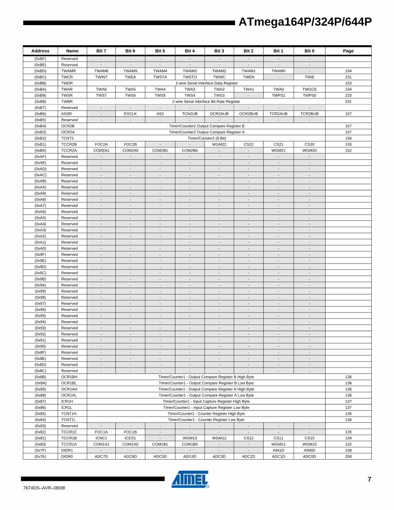
(0xBF) Reserved - - - - - - - -(0xBE) Reserved - - - - - - - -(0xBD) TWAMR TWAM6 TWAM5 TWAM4 TWAM3 TWAM2 TWAM1 TWAM0 - 234(0xBC) TWCR TWINT TWEA TWSTA TWSTO TWWC TWEN - TWIE 231(0xBB) TWDR 2-wire Serial Interface Data Register 233(0xBA) TWAR TWA6 TWA5 TWA4 TWA3 TWA2 TWA1 TWA0 TWGCE 234(0xB9) TWSR TWS7 TWS6 TWS5 TWS4 TWS3 - TWPS1 TWPS0 233(0xB8) TWBR 2-wire Serial Interface Bit Rate Register 231(0xB7) Reserved - - - - - - - -(0xB6) ASSR - EXCLK AS2 TCN2UB OCR2AUB OCR2BUB TCR2AUB TCR2BUB 157(0xB5) Reserved - - - - - - - -(0xB4) OCR2B Timer/Counter2 Output Compare Register B 157(0xB3) OCR2A Timer/Counter2 Output Compare Register A 157(0xB2) TCNT2 Timer/Counter2 (8 Bit) 156(0xB1) TCCR2B FOC2A FOC2B - - WGM22 CS22 CS21 CS20 155(0xB0) TCCR2A COM2A1 COM2A0 COM2B1 COM2B0 - - WGM21 WGM20 152(0xAF) Reserved - - - - - - - -(0xAE) Reserved - - - - - - - -(0xAD) Reserved - - - - - - - -(0xAC) Reserved - - - - - - - -(0xAB) Reserved - - - - - - - -(0xAA) Reserved - - - - - - - -(0xA9) Reserved - - - - - - - -(0xA8) Reserved - - - - - - - -(0xA7) Reserved - - - - - - - -(0xA6) Reserved - - - - - - - -(0xA5) Reserved - - - - - - - -(0xA4) Reserved - - - - - - - -(0xA3) Reserved - - - - - - - -(0xA2) Reserved - - - - - - - -(0xA1) Reserved - - - - - - - -(0xA0) Reserved - - - - - - - -(0x9F) Reserved - - - - - - - -(0x9E) Reserved - - - - - - - -(0x9D) Reserved - - - - - - - -(0x9C) Reserved - - - - - - - -(0x9B) Reserved - - - - - - - -(0x9A) Reserved - - - - - - - -(0x99) Reserved - - - - - - - -(0x98) Reserved - - - - - - - -(0x97) Reserved - - - - - - - -(0x96) Reserved - - - - - - - -(0x95) Reserved - - - - - - - -(0x94) Reserved - - - - - - - -(0x93) Reserved - - - - - - - -(0x92) Reserved - - - - - - - -(0x91) Reserved - - - - - - - -(0x90) Reserved - - - - - - - -(0x8F) Reserved - - - - - - - -(0x8E) Reserved - - - - - - - -(0x8D) Reserved - - - - - - - -(0x8C) Reserved - - - - - - - -(0x8B) OCR1BH Timer/Counter1 - Output Compare Register B High Byte 136 (0x8A) OCR1BL Timer/Counter1 - Output Compare Register B Low Byte 136(0x89) OCR1AH Timer/Counter1 - Output Compare Register A High Byte 136(0x88) OCR1AL Timer/Counter1 - Output Compare Register A Low Byte 136(0x87) ICR1H Timer/Counter1 - Input Capture Register High Byte 137(0x86) ICR1L Timer/Counter1 - Input Capture Register Low Byte 137(0x85) TCNT1H Timer/Counter1 - Counter Register High Byte 136(0x84) TCNT1L Timer/Counter1 - Counter Register Low Byte 136(0x83) Reserved - - - - - - - -(0x82) TCCR1C FOC1A FOC1B - - - - - - 135(0x81) TCCR1B ICNC1 ICES1 - WGM13 WGM12 CS12 CS11 CS10 134(0x80) TCCR1A COM1A1 COM1A0 COM1B1 COM1B0 - - WGM11 WGM10 132(0x7F) DIDR1 - - - - - - AIN1D AIN0D 238(0x7E) DIDR0 ADC7D ADC6D ADC5D ADC4D ADC3D ADC2D ADC1D ADC0D 258
Address Name Bit 7 Bit 6 Bit 5 Bit 4 Bit 3 Bit 2 Bit 1 Bit 0 Page
77674DS–AVR–08/08
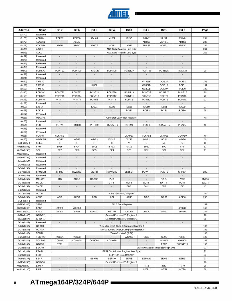
(0x7D) Reserved - - - - - - - -(0x7C) ADMUX REFS1 REFS0 ADLAR MUX4 MUX3 MUX2 MUX1 MUX0 254(0x7B) ADCSRB - ACME - - - ADTS2 ADTS1 ADTS0 237(0x7A) ADCSRA ADEN ADSC ADATE ADIF ADIE ADPS2 ADPS1 ADPS0 256(0x79) ADCH ADC Data Register High byte 257(0x78) ADCL ADC Data Register Low byte 257(0x77) Reserved - - - - - - - -(0x76) Reserved - - - - - - - -(0x75) Reserved - - - - - - - -(0x74) Reserved - - - - - - - -(0x73) PCMSK3 PCINT31 PCINT30 PCINT29 PCINT28 PCINT27 PCINT26 PCINT25 PCINT24 70(0x72) Reserved - - - - - - - -(0x71) Reserved - - - - - - - -(0x70) TIMSK2 - - - - - OCIE2B OCIE2A TOIE2 158(0x6F) TIMSK1 - - ICIE1 - - OCIE1B OCIE1A TOIE1 137(0x6E) TIMSK0 - - - - - OCIE0B OCIE0A TOIE0 109(0x6D) PCMSK2 PCINT23 PCINT22 PCINT21 PCINT20 PCINT19 PCINT18 PCINT17 PCINT16 70(0x6C) PCMSK1 PCINT15 PCINT14 PCINT13 PCINT12 PCINT11 PCINT10 PCINT9 PCINT8 70(0x6B) PCMSK0 PCINT7 PCINT6 PCINT5 PCINT4 PCINT3 PCINT2 PCINT1 PCINT0 71(0x6A) Reserved - - - - - - - -(0x69) EICRA - - ISC21 ISC20 ISC11 ISC10 ISC01 ISC00 67(0x68) PCICR - - - - PCIE3 PCIE2 PCIE1 PCIE0 69(0x67) Reserved - - - - - - - -(0x66) OSCCAL Oscillator Calibration Register 40(0x65) Reserved - - - - - - - -(0x64) PRR PRTWI PRTIM2 PRTIM0 PRUSART1 PRTIM1 PRSPI PRUSART0 PRADC 48(0x63) Reserved - - - - - - - -(0x62) Reserved - - - - - - - -(0x61) CLKPR CLKPCE - - - CLKPS3 CLKPS2 CLKPS1 CLKPS0 40(0x60) WDTCSR WDIF WDIE WDP3 WDCE WDE WDP2 WDP1 WDP0 60
0x3F (0x5F) SREG I T H S V N Z C 100x3E (0x5E) SPH SP15 SP14 SP13 SP12 SP11 SP10 SP9 SP8 110x3D (0x5D) SPL SP7 SP6 SP5 SP4 SP3 SP2 SP1 SP0 110x3C (0x5C) Reserved - - - - - - - -0x3B (0x5B) Reserved - - - - - - - -0x3A (0x5A) Reserved - - - - - - - -0x39 (0x59) Reserved - - - - - - - -0x38 (0x58) Reserved - - - - - - - -0x37 (0x57) SPMCSR SPMIE RWWSB SIGRD RWWSRE BLBSET PGWRT PGERS SPMEN 2900x36 (0x56) Reserved - - - - - - - -0x35 (0x55) MCUCR JTD BODS BODSE PUD - - IVSEL IVCE 91/2740x34 (0x54) MCUSR - - - JTRF WDRF BORF EXTRF PORF 59/2740x33 (0x53) SMCR - - - - SM2 SM1 SM0 SE 470x32 (0x52) Reserved - - - - - - - -0x31 (0x51) OCDR On-Chip Debug Register 2640x30 (0x50) ACSR ACD ACBG ACO ACI ACIE ACIC ACIS1 ACIS0 2560x2F (0x4F) Reserved - - - - - - - -0x2E (0x4E) SPDR SPI 0 Data Register 1690x2D (0x4D) SPSR SPIF0 WCOL0 - - - - - SPI2X0 1680x2C (0x4C) SPCR SPIE0 SPE0 DORD0 MSTR0 CPOL0 CPHA0 SPR01 SPR00 1670x2B (0x4B) GPIOR2 General Purpose I/O Register 2 280x2A (0x4A) GPIOR1 General Purpose I/O Register 1 280x29 (0x49) Reserved - - - - - - - -0x28 (0x48) OCR0B Timer/Counter0 Output Compare Register B 1090x27 (0x47) OCR0A Timer/Counter0 Output Compare Register A 1080x26 (0x46) TCNT0 Timer/Counter0 (8 Bit) 1080x25 (0x45) TCCR0B FOC0A FOC0B - - WGM02 CS02 CS01 CS00 1070x24 (0x44) TCCR0A COM0A1 COM0A0 COM0B1 COM0B0 - - WGM01 WGM00 1090x23 (0x43) GTCCR TSM - - - - - PSR2 PSR54310 1590x22 (0x42) EEARH - - - - EEPROM Address Register High Byte 230x21 (0x41) EEARL EEPROM Address Register Low Byte 230x20 (0x40) EEDR EEPROM Data Register 230x1F (0x3F) EECR - - EEPM1 EEPM0 EERIE EEMWE EEWE EERE 230x1E (0x3E) GPIOR0 General Purpose I/O Register 0 280x1D (0x3D) EIMSK - - - - - INT2 INT1 INT0 680x1C (0x3C) EIFR - - - - - INTF2 INTF1 INTF0 68
Address Name Bit 7 Bit 6 Bit 5 Bit 4 Bit 3 Bit 2 Bit 1 Bit 0 Page
87674DS–AVR–08/08
ATmega164P/324P/644P
ATmega164P/324P/644P
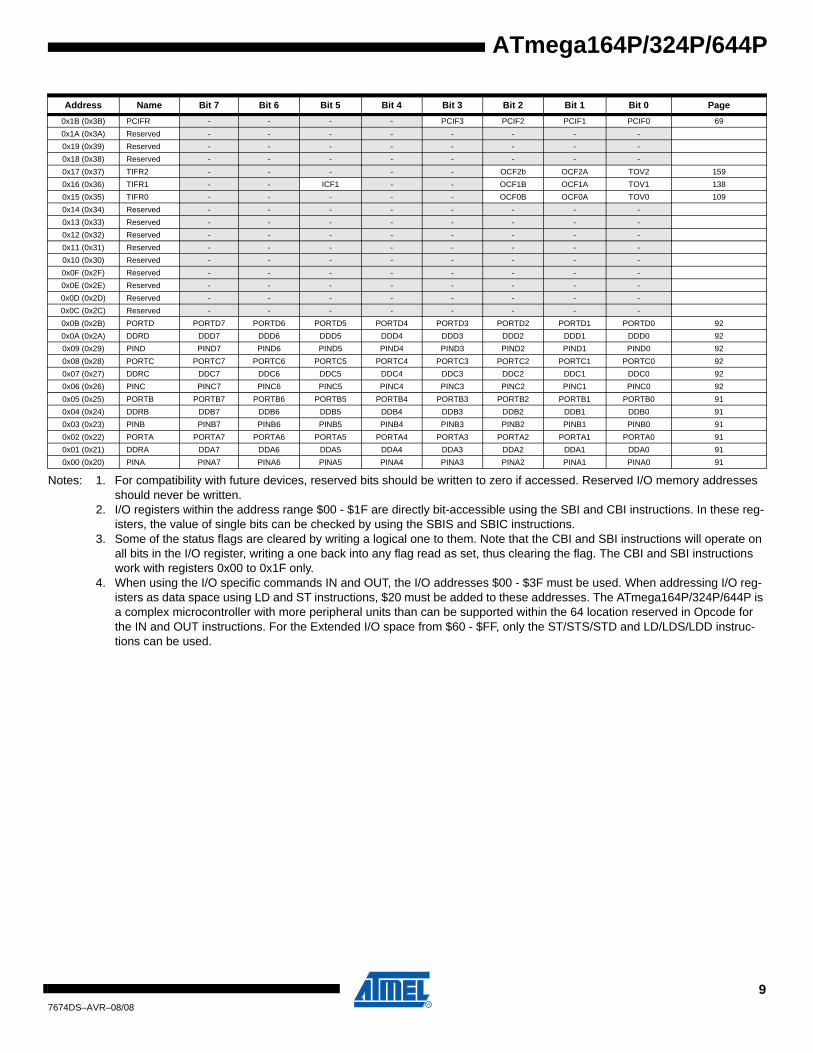
Notes: 1. For compatibility with future devices, reserved bits should be written to zero if accessed. Reserved I/O memory addresses should never be written.
2. I/O registers within the address range $00 - $1F are directly bit-accessible using the SBI and CBI instructions. In these reg-isters, the value of single bits can be checked by using the SBIS and SBIC instructions.
3. Some of the status flags are cleared by writing a logical one to them. Note that the CBI and SBI instructions will operate on all bits in the I/O register, writing a one back into any flag read as set, thus clearing the flag. The CBI and SBI instructions work with registers 0x00 to 0x1F only.
4. When using the I/O specific commands IN and OUT, the I/O addresses $00 - $3F must be used. When addressing I/O reg-isters as data space using LD and ST instructions, $20 must be added to these addresses. The ATmega164P/324P/644P is a complex microcontroller with more peripheral units than can be supported within the 64 location reserved in Opcode for the IN and OUT instructions. For the Extended I/O space from $60 - $FF, only the ST/STS/STD and LD/LDS/LDD instruc-tions can be used.
0x1B (0x3B) PCIFR - - - - PCIF3 PCIF2 PCIF1 PCIF0 690x1A (0x3A) Reserved - - - - - - - -0x19 (0x39) Reserved - - - - - - - -0x18 (0x38) Reserved - - - - - - - -0x17 (0x37) TIFR2 - - - - - OCF2b OCF2A TOV2 1590x16 (0x36) TIFR1 - - ICF1 - - OCF1B OCF1A TOV1 1380x15 (0x35) TIFR0 - - - - - OCF0B OCF0A TOV0 1090x14 (0x34) Reserved - - - - - - - -0x13 (0x33) Reserved - - - - - - - -0x12 (0x32) Reserved - - - - - - - -0x11 (0x31) Reserved - - - - - - - -0x10 (0x30) Reserved - - - - - - - -0x0F (0x2F) Reserved - - - - - - - -0x0E (0x2E) Reserved - - - - - - - -0x0D (0x2D) Reserved - - - - - - - -0x0C (0x2C) Reserved - - - - - - - -0x0B (0x2B) PORTD PORTD7 PORTD6 PORTD5 PORTD4 PORTD3 PORTD2 PORTD1 PORTD0 920x0A (0x2A) DDRD DDD7 DDD6 DDD5 DDD4 DDD3 DDD2 DDD1 DDD0 920x09 (0x29) PIND PIND7 PIND6 PIND5 PIND4 PIND3 PIND2 PIND1 PIND0 920x08 (0x28) PORTC PORTC7 PORTC6 PORTC5 PORTC4 PORTC3 PORTC2 PORTC1 PORTC0 920x07 (0x27) DDRC DDC7 DDC6 DDC5 DDC4 DDC3 DDC2 DDC1 DDC0 920x06 (0x26) PINC PINC7 PINC6 PINC5 PINC4 PINC3 PINC2 PINC1 PINC0 920x05 (0x25) PORTB PORTB7 PORTB6 PORTB5 PORTB4 PORTB3 PORTB2 PORTB1 PORTB0 910x04 (0x24) DDRB DDB7 DDB6 DDB5 DDB4 DDB3 DDB2 DDB1 DDB0 910x03 (0x23) PINB PINB7 PINB6 PINB5 PINB4 PINB3 PINB2 PINB1 PINB0 910x02 (0x22) PORTA PORTA7 PORTA6 PORTA5 PORTA4 PORTA3 PORTA2 PORTA1 PORTA0 910x01 (0x21) DDRA DDA7 DDA6 DDA5 DDA4 DDA3 DDA2 DDA1 DDA0 910x00 (0x20) PINA PINA7 PINA6 PINA5 PINA4 PINA3 PINA2 PINA1 PINA0 91
Address Name Bit 7 Bit 6 Bit 5 Bit 4 Bit 3 Bit 2 Bit 1 Bit 0 Page
97674DS–AVR–08/08
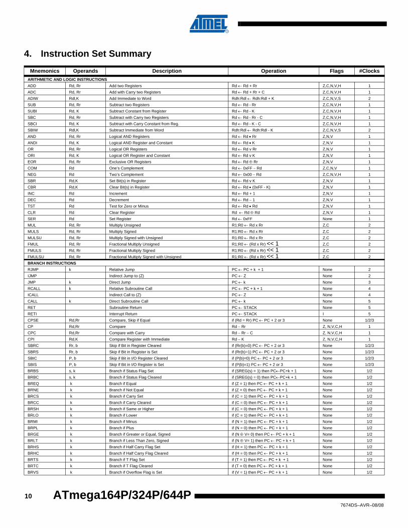
4. Instruction Set SummaryMnemonics Operands Description Operation Flags #Clocks
ARITHMETIC AND LOGIC INSTRUCTIONSADD Rd, Rr Add two Registers Rd ← Rd + Rr Z,C,N,V,H 1ADC Rd, Rr Add with Carry two Registers Rd ← Rd + Rr + C Z,C,N,V,H 1ADIW Rdl,K Add Immediate to Word Rdh:Rdl ← Rdh:Rdl + K Z,C,N,V,S 2SUB Rd, Rr Subtract two Registers Rd ← Rd - Rr Z,C,N,V,H 1SUBI Rd, K Subtract Constant from Register Rd ← Rd - K Z,C,N,V,H 1SBC Rd, Rr Subtract with Carry two Registers Rd ← Rd - Rr - C Z,C,N,V,H 1SBCI Rd, K Subtract with Carry Constant from Reg. Rd ← Rd - K - C Z,C,N,V,H 1SBIW Rdl,K Subtract Immediate from Word Rdh:Rdl ← Rdh:Rdl - K Z,C,N,V,S 2AND Rd, Rr Logical AND Registers Rd ← Rd • Rr Z,N,V 1ANDI Rd, K Logical AND Register and Constant Rd ← Rd • K Z,N,V 1OR Rd, Rr Logical OR Registers Rd ← Rd v Rr Z,N,V 1ORI Rd, K Logical OR Register and Constant Rd ← Rd v K Z,N,V 1EOR Rd, Rr Exclusive OR Registers Rd ← Rd ⊕ Rr Z,N,V 1COM Rd One’s Complement Rd ← 0xFF − Rd Z,C,N,V 1NEG Rd Two’s Complement Rd ← 0x00 − Rd Z,C,N,V,H 1SBR Rd,K Set Bit(s) in Register Rd ← Rd v K Z,N,V 1CBR Rd,K Clear Bit(s) in Register Rd ← Rd • (0xFF - K) Z,N,V 1INC Rd Increment Rd ← Rd + 1 Z,N,V 1DEC Rd Decrement Rd ← Rd − 1 Z,N,V 1TST Rd Test for Zero or Minus Rd ← Rd • Rd Z,N,V 1CLR Rd Clear Register Rd ← Rd ⊕ Rd Z,N,V 1SER Rd Set Register Rd ← 0xFF None 1MUL Rd, Rr Multiply Unsigned R1:R0 ← Rd x Rr Z,C 2MULS Rd, Rr Multiply Signed R1:R0 ← Rd x Rr Z,C 2MULSU Rd, Rr Multiply Signed with Unsigned R1:R0 ← Rd x Rr Z,C 2FMUL Rd, Rr Fractional Multiply Unsigned R1:R0 ← (Rd x Rr) << 1 Z,C 2FMULS Rd, Rr Fractional Multiply Signed R1:R0 ← (Rd x Rr) << 1 Z,C 2FMULSU Rd, Rr Fractional Multiply Signed with Unsigned R1:R0 ← (Rd x Rr) << 1 Z,C 2BRANCH INSTRUCTIONSRJMP k Relative Jump PC ← PC + k + 1 None 2IJMP Indirect Jump to (Z) PC ← Z None 2JMP k Direct Jump PC ← k None 3RCALL k Relative Subroutine Call PC ← PC + k + 1 None 4ICALL Indirect Call to (Z) PC ← Z None 4CALL k Direct Subroutine Call PC ← k None 5RET Subroutine Return PC ← STACK None 5RETI Interrupt Return PC ← STACK I 5CPSE Rd,Rr Compare, Skip if Equal if (Rd = Rr) PC ← PC + 2 or 3 None 1/2/3CP Rd,Rr Compare Rd − Rr Z, N,V,C,H 1 CPC Rd,Rr Compare with Carry Rd − Rr − C Z, N,V,C,H 1CPI Rd,K Compare Register with Immediate Rd − K Z, N,V,C,H 1SBRC Rr, b Skip if Bit in Register Cleared if (Rr(b)=0) PC ← PC + 2 or 3 None 1/2/3SBRS Rr, b Skip if Bit in Register is Set if (Rr(b)=1) PC ← PC + 2 or 3 None 1/2/3SBIC P, b Skip if Bit in I/O Register Cleared if (P(b)=0) PC ← PC + 2 or 3 None 1/2/3SBIS P, b Skip if Bit in I/O Register is Set if (P(b)=1) PC ← PC + 2 or 3 None 1/2/3BRBS s, k Branch if Status Flag Set if (SREG(s) = 1) then PC←PC+k + 1 None 1/2BRBC s, k Branch if Status Flag Cleared if (SREG(s) = 0) then PC←PC+k + 1 None 1/2BREQ k Branch if Equal if (Z = 1) then PC ← PC + k + 1 None 1/2BRNE k Branch if Not Equal if (Z = 0) then PC ← PC + k + 1 None 1/2BRCS k Branch if Carry Set if (C = 1) then PC ← PC + k + 1 None 1/2BRCC k Branch if Carry Cleared if (C = 0) then PC ← PC + k + 1 None 1/2BRSH k Branch if Same or Higher if (C = 0) then PC ← PC + k + 1 None 1/2BRLO k Branch if Lower if (C = 1) then PC ← PC + k + 1 None 1/2BRMI k Branch if Minus if (N = 1) then PC ← PC + k + 1 None 1/2BRPL k Branch if Plus if (N = 0) then PC ← PC + k + 1 None 1/2BRGE k Branch if Greater or Equal, Signed if (N ⊕ V= 0) then PC ← PC + k + 1 None 1/2BRLT k Branch if Less Than Zero, Signed if (N ⊕ V= 1) then PC ← PC + k + 1 None 1/2BRHS k Branch if Half Carry Flag Set if (H = 1) then PC ← PC + k + 1 None 1/2BRHC k Branch if Half Carry Flag Cleared if (H = 0) then PC ← PC + k + 1 None 1/2BRTS k Branch if T Flag Set if (T = 1) then PC ← PC + k + 1 None 1/2BRTC k Branch if T Flag Cleared if (T = 0) then PC ← PC + k + 1 None 1/2BRVS k Branch if Overflow Flag is Set if (V = 1) then PC ← PC + k + 1 None 1/2
107674DS–AVR–08/08
ATmega164P/324P/644P
ATmega164P/324P/644P
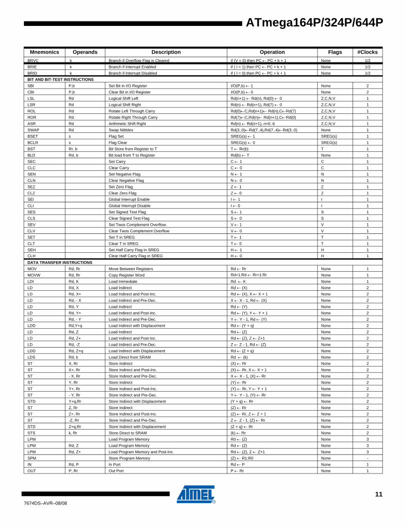
BRVC k Branch if Overflow Flag is Cleared if (V = 0) then PC ← PC + k + 1 None 1/2BRIE k Branch if Interrupt Enabled if ( I = 1) then PC ← PC + k + 1 None 1/2BRID k Branch if Interrupt Disabled if ( I = 0) then PC ← PC + k + 1 None 1/2BIT AND BIT-TEST INSTRUCTIONSSBI P,b Set Bit in I/O Register I/O(P,b) ← 1 None 2CBI P,b Clear Bit in I/O Register I/O(P,b) ← 0 None 2LSL Rd Logical Shift Left Rd(n+1) ← Rd(n), Rd(0) ← 0 Z,C,N,V 1LSR Rd Logical Shift Right Rd(n) ← Rd(n+1), Rd(7) ← 0 Z,C,N,V 1ROL Rd Rotate Left Through Carry Rd(0)←C,Rd(n+1)← Rd(n),C←Rd(7) Z,C,N,V 1ROR Rd Rotate Right Through Carry Rd(7)←C,Rd(n)← Rd(n+1),C←Rd(0) Z,C,N,V 1ASR Rd Arithmetic Shift Right Rd(n) ← Rd(n+1), n=0..6 Z,C,N,V 1SWAP Rd Swap Nibbles Rd(3..0)←Rd(7..4),Rd(7..4)←Rd(3..0) None 1BSET s Flag Set SREG(s) ← 1 SREG(s) 1BCLR s Flag Clear SREG(s) ← 0 SREG(s) 1BST Rr, b Bit Store from Register to T T ← Rr(b) T 1BLD Rd, b Bit load from T to Register Rd(b) ← T None 1SEC Set Carry C ← 1 C 1CLC Clear Carry C ← 0 C 1SEN Set Negative Flag N ← 1 N 1CLN Clear Negative Flag N ← 0 N 1SEZ Set Zero Flag Z ← 1 Z 1CLZ Clear Zero Flag Z ← 0 Z 1SEI Global Interrupt Enable I ← 1 I 1CLI Global Interrupt Disable I ← 0 I 1SES Set Signed Test Flag S ← 1 S 1CLS Clear Signed Test Flag S ← 0 S 1SEV Set Twos Complement Overflow. V ← 1 V 1CLV Clear Twos Complement Overflow V ← 0 V 1SET Set T in SREG T ← 1 T 1CLT Clear T in SREG T ← 0 T 1SEH Set Half Carry Flag in SREG H ← 1 H 1CLH Clear Half Carry Flag in SREG H ← 0 H 1
DATA TRANSFER INSTRUCTIONSMOV Rd, Rr Move Between Registers Rd ← Rr None 1MOVW Rd, Rr Copy Register Word Rd+1:Rd ← Rr+1:Rr None 1LDI Rd, K Load Immediate Rd ← K None 1LD Rd, X Load Indirect Rd ← (X) None 2LD Rd, X+ Load Indirect and Post-Inc. Rd ← (X), X ← X + 1 None 2LD Rd, - X Load Indirect and Pre-Dec. X ← X - 1, Rd ← (X) None 2LD Rd, Y Load Indirect Rd ← (Y) None 2LD Rd, Y+ Load Indirect and Post-Inc. Rd ← (Y), Y ← Y + 1 None 2LD Rd, - Y Load Indirect and Pre-Dec. Y ← Y - 1, Rd ← (Y) None 2LDD Rd,Y+q Load Indirect with Displacement Rd ← (Y + q) None 2LD Rd, Z Load Indirect Rd ← (Z) None 2LD Rd, Z+ Load Indirect and Post-Inc. Rd ← (Z), Z ← Z+1 None 2LD Rd, -Z Load Indirect and Pre-Dec. Z ← Z - 1, Rd ← (Z) None 2LDD Rd, Z+q Load Indirect with Displacement Rd ← (Z + q) None 2LDS Rd, k Load Direct from SRAM Rd ← (k) None 2ST X, Rr Store Indirect (X) ← Rr None 2ST X+, Rr Store Indirect and Post-Inc. (X) ← Rr, X ← X + 1 None 2ST - X, Rr Store Indirect and Pre-Dec. X ← X - 1, (X) ← Rr None 2ST Y, Rr Store Indirect (Y) ← Rr None 2ST Y+, Rr Store Indirect and Post-Inc. (Y) ← Rr, Y ← Y + 1 None 2ST - Y, Rr Store Indirect and Pre-Dec. Y ← Y - 1, (Y) ← Rr None 2STD Y+q,Rr Store Indirect with Displacement (Y + q) ← Rr None 2ST Z, Rr Store Indirect (Z) ← Rr None 2ST Z+, Rr Store Indirect and Post-Inc. (Z) ← Rr, Z ← Z + 1 None 2ST -Z, Rr Store Indirect and Pre-Dec. Z ← Z - 1, (Z) ← Rr None 2STD Z+q,Rr Store Indirect with Displacement (Z + q) ← Rr None 2STS k, Rr Store Direct to SRAM (k) ← Rr None 2LPM Load Program Memory R0 ← (Z) None 3LPM Rd, Z Load Program Memory Rd ← (Z) None 3LPM Rd, Z+ Load Program Memory and Post-Inc Rd ← (Z), Z ← Z+1 None 3SPM Store Program Memory (Z) ← R1:R0 None -IN Rd, P In Port Rd ← P None 1OUT P, Rr Out Port P ← Rr None 1
Mnemonics Operands Description Operation Flags #Clocks
117674DS–AVR–08/08
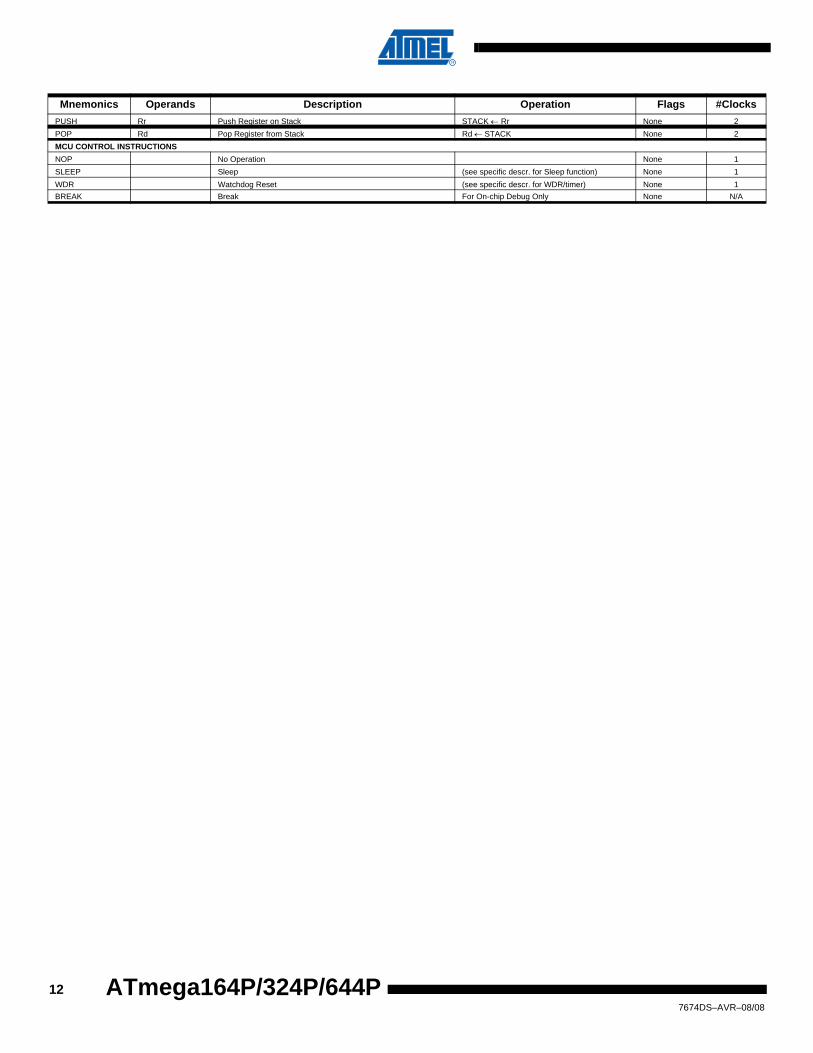
PUSH Rr Push Register on Stack STACK ← Rr None 2POP Rd Pop Register from Stack Rd ← STACK None 2MCU CONTROL INSTRUCTIONSNOP No Operation None 1SLEEP Sleep (see specific descr. for Sleep function) None 1WDR Watchdog Reset (see specific descr. for WDR/timer) None 1BREAK Break For On-chip Debug Only None N/A
Mnemonics Operands Description Operation Flags #Clocks
127674DS–AVR–08/08
ATmega164P/324P/644P
ATmega164P/324P/644P
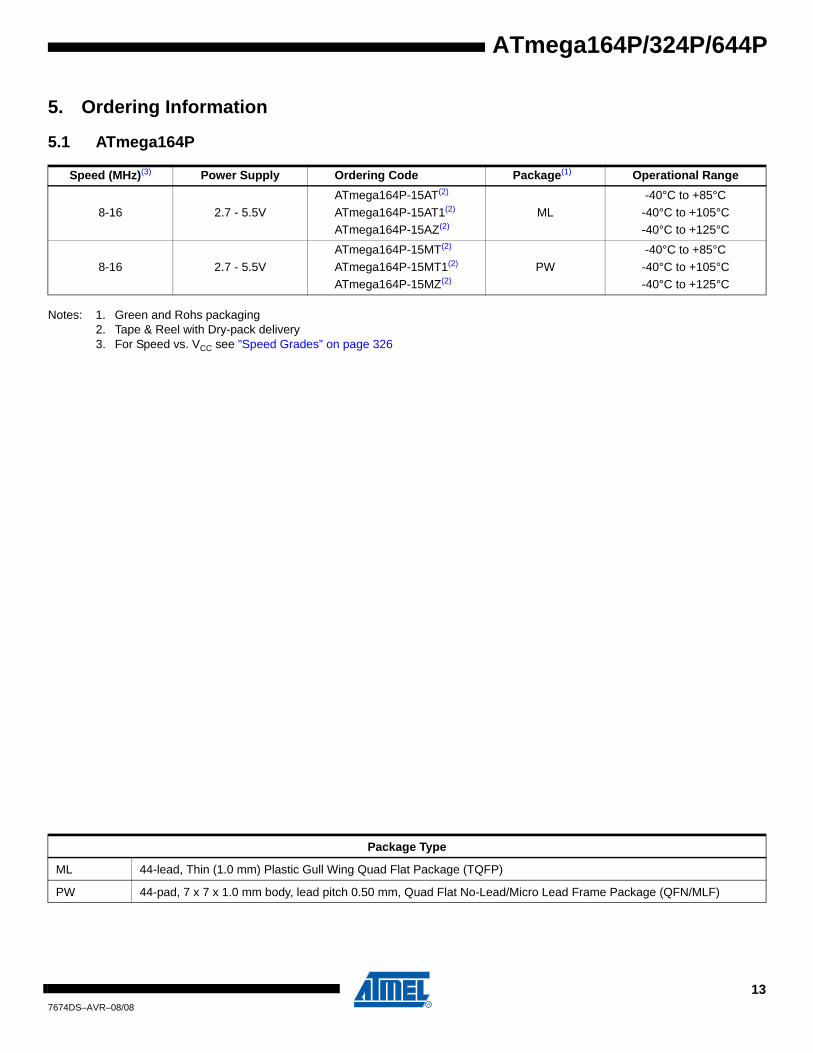
5. Ordering Information
5.1 ATmega164P
Notes: 1. Green and Rohs packaging2. Tape & Reel with Dry-pack delivery3. For Speed vs. VCC see ”Speed Grades” on page 326
Speed (MHz)(3) Power Supply Ordering Code Package(1) Operational Range
8-16 2.7 - 5.5VATmega164P-15AT(2)
ATmega164P-15AT1(2)
ATmega164P-15AZ(2)ML
-40°C to +85°C-40°C to +105°C-40°C to +125°C
8-16 2.7 - 5.5VATmega164P-15MT(2)
ATmega164P-15MT1(2)
ATmega164P-15MZ(2)PW
-40°C to +85°C-40°C to +105°C-40°C to +125°C
Package Type
ML 44-lead, Thin (1.0 mm) Plastic Gull Wing Quad Flat Package (TQFP)
PW 44-pad, 7 x 7 x 1.0 mm body, lead pitch 0.50 mm, Quad Flat No-Lead/Micro Lead Frame Package (QFN/MLF)
137674DS–AVR–08/08
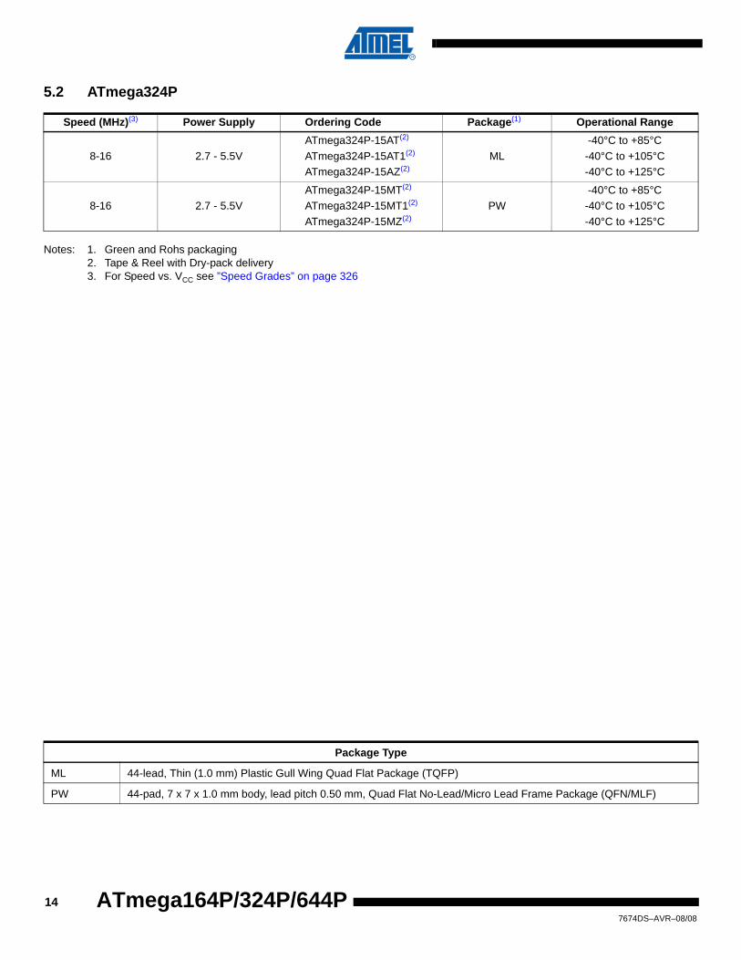
5.2 ATmega324P
Notes: 1. Green and Rohs packaging2. Tape & Reel with Dry-pack delivery3. For Speed vs. VCC see ”Speed Grades” on page 326
Speed (MHz)(3) Power Supply Ordering Code Package(1) Operational Range
8-16 2.7 - 5.5VATmega324P-15AT(2)
ATmega324P-15AT1(2)
ATmega324P-15AZ(2)ML
-40°C to +85°C-40°C to +105°C-40°C to +125°C
8-16 2.7 - 5.5VATmega324P-15MT(2)
ATmega324P-15MT1(2)
ATmega324P-15MZ(2)PW
-40°C to +85°C-40°C to +105°C-40°C to +125°C
Package Type
ML 44-lead, Thin (1.0 mm) Plastic Gull Wing Quad Flat Package (TQFP)
PW 44-pad, 7 x 7 x 1.0 mm body, lead pitch 0.50 mm, Quad Flat No-Lead/Micro Lead Frame Package (QFN/MLF)
147674DS–AVR–08/08
ATmega164P/324P/644P
ATmega164P/324P/644P
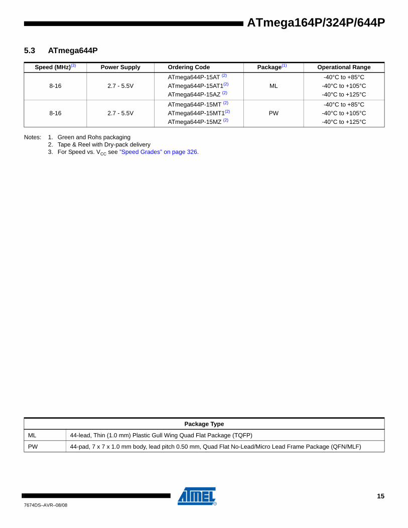
5.3 ATmega644P
Notes: 1. Green and Rohs packaging2. Tape & Reel with Dry-pack delivery3. For Speed vs. VCC see ”Speed Grades” on page 326.
Speed (MHz)(3) Power Supply Ordering Code Package(1) Operational Range
8-16 2.7 - 5.5VATmega644P-15AT (2)
ATmega644P-15AT1(2)
ATmega644P-15AZ (2)ML
-40°C to +85°C-40°C to +105°C-40°C to +125°C
8-16 2.7 - 5.5VATmega644P-15MT (2)
ATmega644P-15MT1(2)
ATmega644P-15MZ (2)PW
-40°C to +85°C-40°C to +105°C-40°C to +125°C
Package Type
ML 44-lead, Thin (1.0 mm) Plastic Gull Wing Quad Flat Package (TQFP)
PW 44-pad, 7 x 7 x 1.0 mm body, lead pitch 0.50 mm, Quad Flat No-Lead/Micro Lead Frame Package (QFN/MLF)
157674DS–AVR–08/08
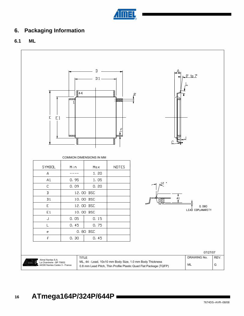
6. Packaging Information
6.1 ML
167674DS–AVR–08/08
ATmega164P/324P/644P
ATmega164P/324P/644P
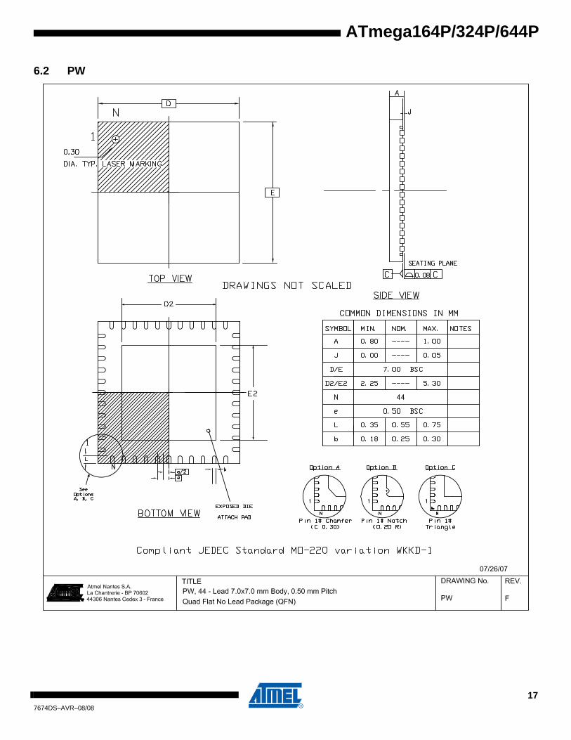
6.2 PW
177674DS–AVR–08/08
187674DS–AVR–08/08
ATmega164P/324P/644P
ATmega164P/324P/644P
7. Errata
7.1 ATmega164P Rev. A
No known Errata.
7.2 ATmega324P Rev. A
No known Errata.
7.3 ATmega644P Rev. A
No known Errata.
8. Datasheet Revision History
Please note that the referring page numbers in this section are referred to this document. Thereferring revision in this section are referring to the document revision.
8.1 Rev. 7674C -05/08
1. VIL reset pin update. Section 26.1 on page 325.2. Updated EEPROM endurance. See ”Features” on page 1.
8.2 Rev. 7674B -01/08
1. Update to electrical characteristics after product characterization.8.3 Rev. 7674A - 04/07
1. Initial Automotive revision2. Insertion of specific § for automative quality references3. DC and Frequency adapted to Automotive temperature range4. Part numbering and package selection according to Automotive rules5. Current Consumption adapted based on Industrial electrical characterization.
197674DS–AVR–08/08
9. Datasheet Revision History
Please note that the referring page numbers in this section are referred to this document. Thereferring revision in this section are referring to the document revision.
9.1 Rev. 7674D -08/08
1. Added ADC differential mode electrical characteristics for ATMega164 Table 26-10 on page 334.
2. Removed Ramp Z register.
9.2 Rev. 7674C -05/08
1. VIL reset pin update. Section 26.1 on page 325.2. Updated EEPROM endurance. See ”Features” on page 1.
9.3 Rev. 7674B -01/08
1. Update to electrical characteristics after product characterization.
9.4 Rev. 7674A - 04/07
1. Initial Automotive revision2. Insertion of specific § for automative quality references3. DC and Frequency adapted to Automotive temperature range4. Part numbering and package selection according to Automotive rules5. Current Consumption adapted based on Industrial electrical characterization.
207674DS–AVR–08/08
ATmega164P/324P/644P
Headquarters International
Atmel Corporation2325 Orchard ParkwaySan Jose, CA 95131USATel: 1(408) 441-0311Fax: 1(408) 487-2600
Atmel AsiaRoom 1219Chinachem Golden Plaza77 Mody Road TsimshatsuiEast KowloonHong KongTel: (852) 2721-9778Fax: (852) 2722-1369
Atmel EuropeLe Krebs8, Rue Jean-Pierre TimbaudBP 30978054 Saint-Quentin-en-Yvelines CedexFranceTel: (33) 1-30-60-70-00 Fax: (33) 1-30-60-71-11
Atmel Japan9F, Tonetsu Shinkawa Bldg.1-24-8 ShinkawaChuo-ku, Tokyo 104-0033JapanTel: (81) 3-3523-3551Fax: (81) 3-3523-7581
Product Contact
Web Sitewww.atmel.com
Technical [email protected]
Sales Contactwww.atmel.com/contacts
Literature Requestswww.atmel.com/literature
Disclaimer: The information in this document is provided in connection with Atmel products. No license, express or implied, by estoppel or otherwise, to anyintellectual property right is granted by this document or in connection with the sale of Atmel products. EXCEPT AS SET FORTH IN ATMEL’S TERMS AND CONDI-TIONS OF SALE LOCATED ON ATMEL’S WEB SITE, ATMEL ASSUMES NO LIABILITY WHATSOEVER AND DISCLAIMS ANY EXPRESS, IMPLIED OR STATUTORYWARRANTY RELATING TO ITS PRODUCTS INCLUDING, BUT NOT LIMITED TO, THE IMPLIED WARRANTY OF MERCHANTABILITY, FITNESS FOR A PARTICULARPURPOSE, OR NON-INFRINGEMENT. IN NO EVENT SHALL ATMEL BE LIABLE FOR ANY DIRECT, INDIRECT, CONSEQUENTIAL, PUNITIVE, SPECIAL OR INCIDEN-TAL DAMAGES (INCLUDING, WITHOUT LIMITATION, DAMAGES FOR LOSS OF PROFITS, BUSINESS INTERRUPTION, OR LOSS OF INFORMATION) ARISING OUTOF THE USE OR INABILITY TO USE THIS DOCUMENT, EVEN IF ATMEL HAS BEEN ADVISED OF THE POSSIBILITY OF SUCH DAMAGES. Atmel makes norepresentations or warranties with respect to the accuracy or completeness of the contents of this document and reserves the right to make changes to specificationsand product descriptions at any time without notice. Atmel does not make any commitment to update the information contained herein. Unless specifically providedotherwise, Atmel products are not suitable for, and shall not be used in, automotive applications. Atmel’s products are not intended, authorized, or warranted for useas components in applications intended to support or sustain life.
7674DS–AVR–08/08
![Atmel AT30TS750 - Digi-Key Sheets/Atmel... · Atmel AT30TS750 [DATASHEET] 4 8749C–DTS–6/12 1. Description The Atmel® AT30TS750 is a complete, precise temperature monitoring device](https://img.pdfslide.net/doc/110x75/5eaf2d045afdd00c517ed97f/atmel-at30ts750-digi-key-sheetsatmel-atmel-at30ts750-datasheet-4-8749cadtsa612.jpg)


![Atmel AT24C512C - Digi-Key Sheets/Atmel PDFs...Atmel AT24C512C [DATASHEET] 2 8720C–SEEPR–7/12 1. Pin Configurations and Pinouts Figure 1. Pin Configurations 2. Absolute Maximum](https://img.pdfslide.net/doc/110x75/5b0293b37f8b9a65618f6d93/atmel-at24c512c-digi-key-sheetsatmel-pdfsatmel-at24c512c-datasheet-2-8720cseepr712.jpg)
![ATA6837 - Digi-Key Sheets/Atmel PDFs...Atmel ATA6837 [DATASHEET] 6 4953H–AUTO–03/12 Table 3-2. Output Data Protocol Bit Output (Status) Register Function 0 TP Temperature prewarning:](https://img.pdfslide.net/doc/110x75/5b0243737f8b9a54578f7114/ata6837-digi-key-sheetsatmel-pdfsatmel-ata6837-datasheet-6-4953hauto0312.jpg)