Embed Size (px)
Citation preview
A 10-b 800MS/s Time-Interleaved SAR ADC with Fast Timing-Skew Calibration
Jeonggoo Song, Kareem Ragab, Xiyuan Tang, and Nan Sun
University of Texas at Austin, Austin, TX, USA
Email: [email protected], [email protected]
Abstract— This paper presents a time-interleaved (TI)
successive-approximation-register (SAR) ADC with a fast
variance-based timing-skew calibration technique. It uses a single
comparator-based window detector to calibrate the timing skew.
It has low-hardware cost and 104 times faster convergence speed
compared to prior variance-based timing skew calibration
technique. The proposed technique brings collateral benefits of
offset mismatch calibration. A prototype 10-b 800MS/s ADC in
40nm CMOS achieves Nyquist-rate SNDR of 48 dB and consumes
9.8mW, leading to a Walden FoM of 59-fJ/conversion-step.
Keywords – time-interleaved ADC, variance-based timing-skew
calibration
I. INTRODUCTION
TI SAR ADC is well-known for its energy-efficiency for
high-speed and medium-resolution applications. However,
without calibrating mismatches (e.g. gain error, offset error, and
timing skew), it is nontrivial to achieve good linearity. Among
all, timing skew mismatch, which aggravates at high input
frequencies, is known to be a linearity bottleneck. Various
timing skew calibration techniques have been developed. In [1],
a dedicated reference ADC was used. The reference ADC is a
replica of the TI ADC channels and runs at fs/(N+1), where N is
the number of TI channels. Having a full-blown ADC replica
increases power, especially for a small N. Additionally, it sets a
lower limit on the alignment (beat) period of the reference and
each ADC channel to N(N+1) clock cycles, reducing the
calibration speed. Furthermore, the alternatingly operated
reference channel introduces spurs by periodically changing
ADC input impedance. The reference channel is simplified to a
single comparator which reduces power [2]. However, its
convergence speed is slow for random inputs due to large
autocorrelation estimation errors. Flash-assisted time-
interleaved (FATI) SAR addresses these problems by having a
low-resolution flash ADC running at the ADC full rate [3].
Timing skew is minimized by reducing the variance of the
difference between each channel’s output and the flash ADC.
However, the flash ADC consumes large power. Moreover, the
convergence speed is still slow when operating in the
background with random inputs that cause large fluctuations in
the variance estimation. This paper presents a novel variance-based timing-skew
calibration technique for TI ADC. It exploits the relationship between the comparator input and its decision time to identify input samples that are close to the comparator threshold. By using only these samples, the variance computation has much less fluctuation. As a result, the proposed technique substantially reduces the number of samples needed to obtain an accurate variance estimation which consequently significantly boosts the convergence speed. Our prototype ADC requires only 105 input
samples per calibration step, which is 4 orders of magnitude smaller than that of the prior variance-based timing-skew calibration technique of [3]. Furthermore, the proposed technique also obviates the need for a flash ADC; instead, it only requires a single comparator-based window detector, which reduces hardware overhead and power.
This paper is organized as follows. Section II introduces the proposed timing-skew calibration technique. Section III presents the convergence time analysis. Measurement results are discussed in Section IV. Conclusion is brought up in Section V.
II. PROPOSED TIMING-SKEW CALIBRATION TECHNIQUE
A. Proposed Time-Interleaved ADC Architecture
Fig. 1 shows the architecture of a 4-way TI SAR with the
proposed timing-skew calibration technique. It consists of 4
SAR ADCs, a window detector based reference channel, an
output MUX, a multi-phase clock generator, variable delay
lines (VDLs), and a timing-skew calibration engine. The
window detector operates at full ADC rate, so that the ADC
input impedance is constant at every clock cycle, eliminating
potential spurs. The calibration engine uses the window
detector to check whether a sampled input 𝑉𝑖𝑛 is within a fixed
window, i.e., |𝑉𝑖𝑛| ≤ 𝑊, where W is the window width. This
window detector consists of a replica sampling network, a
dynamic latch comparator, a current-starved inverter chain, and
a flag DFF. The window flag f is raised when the clock signal
arrives at the DFF before the XOR output goes high. The
inverter chain is configured so that 𝜏𝑑𝑒𝑙𝑎𝑦 = 𝜏𝑐𝑜𝑚𝑝,𝐿𝑆𝐵 + 𝜏𝑋𝑂𝑅 ,
where 𝜏𝑋𝑂𝑅 is the XOR delay and 𝜏𝑐𝑜𝑚𝑝,𝐿𝑆𝐵 is the comparator
delay when |𝑉𝑖𝑛| = 𝑊. If |𝑉𝑖𝑛| ≤ 𝑊, regeneration time of the
comparator is longer than 𝜏𝑐𝑜𝑚𝑝,𝐿𝑆𝐵 and the flag f is raised (f =
1). On the other hand, if |𝑉𝑖𝑛| > 𝑊, the flag f is not raised (f =
0). W can be tuned by adjusting 𝜏𝑑𝑒𝑙𝑎𝑦. Increasing
𝜏𝑑𝑒𝑙𝑎𝑦 reduces W, while reducing 𝜏𝑑𝑒𝑙𝑎𝑦 enlarges W. 𝜏𝑑𝑒𝑙𝑎𝑦 is
adjusted by changing the bias current into the current-starved
inverter chain of the window detector.
B. Proposed Timing-skew Calibration Technique
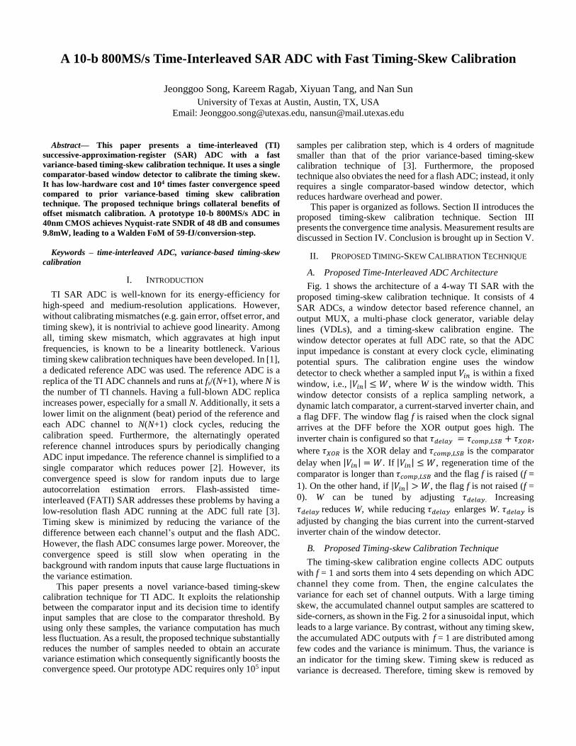
The timing-skew calibration engine collects ADC outputs
with f = 1 and sorts them into 4 sets depending on which ADC
channel they come from. Then, the engine calculates the
variance for each set of channel outputs. With a large timing
skew, the accumulated channel output samples are scattered to
side-corners, as shown in the Fig. 2 for a sinusoidal input, which
leads to a large variance. By contrast, without any timing skew,
the accumulated ADC outputs with f = 1 are distributed among
few codes and the variance is minimum. Thus, the variance is
an indicator for the timing skew. Timing skew is reduced as
variance is decreased. Therefore, timing skew is removed by
Fig. 1. A 4-way time-interleaved SAR with the proposed fast variance-based timing skew calibration technique.
Fig. 2. Basic idea of the proposed variance-based timing-skew calibration.
minimizing the variance. The VDL is controlled by the
calibration engine to align the sampling edges of the reference
channel and 4 ADCs. VDL delays are added or removed in the
direction achieving lower variance. The digitally controlled
VDL of this work has 5b binary-weighted control codes for fine
delay tuning of 300fs per step and 2b coarse control codes with
2ps per step.
III. CONVERGENCE TIME ANALYSIS
Convergence time is an important factor for any timing-skew
calibration algorithm. Convergence time must be short enough
to keep track of temperature changes because the delay is highly
sensitive to temperature. For the proposed technique,
convergence time is limited by the number of input samples, M,
that is required to obtain an accurate estimation of the variance.
The key parameter that sets M is the window width W. At first
glance, it seems that a large W is preferred as it increases the
number of ADC inputs falling into the window, and thus, can
reduce error in variance estimation by averaging. Nevertheless,
a large W greatly increases the variance fluctuation for ADC
samples with f = 1. This significantly increase the convergence
time, as a much bigger number of input samples should be
averaged in order to obtain an accurate estimation of the
variance.
To prove this, let us first calculate the variance of an ADC
channel's outputs with f = 1, denoted as 𝜎𝑣2(𝜏):
𝜎𝑣2(𝜏) ≡ 𝑉𝑎𝑟(𝑉𝑖𝑛(𝑡 + 𝜏)|𝑓=1 )
≅ 𝑉𝑎𝑟(𝑉𝑖𝑛(𝑡)|𝑓=1) + 𝜏2 ⋅ 𝑉𝑎𝑟 (𝑑𝑉𝑖𝑛
𝑑𝑡) (1)
where is the timing skew between the ADC channel and the
window detector. Here, in deriving (1), we have exploited the
fact that 𝑉𝑖𝑛(𝑡) and 𝑑𝑉𝑖𝑛/𝑑𝑡 can be treated as two uncorrelated
random variables. The 2nd term on the right hand side of (1)
carries information on and is the “signal” component in the
time skew calibration process. By contrast, the 1st term on the
right side of (1) contributes only “noise” in the overall variance
estimation. We denote the RMS of the estimation error of (1)
term as 𝑁𝑒𝑠𝑡(𝜏). It can be derived that [4]:
𝑁𝑒𝑠𝑡(𝜏) ≈ √1
𝑀 ⋅ 𝑃(𝑓 = 1)∙ 𝑉𝑎𝑟(𝑉𝑖𝑛
2 (𝑡 + 𝜏)|𝑓=1)
≈ √1
𝑀 ⋅ 𝑝0 ⋅ 𝑊∙ 𝑉𝑎𝑟 ((𝑉𝑖𝑛 + 𝜏
𝑑𝑉𝑖𝑛
𝑑𝑡)
2
|𝑓=1)
= √1
𝑀⋅𝑝0⋅𝑊∙ (
4
45𝑊4 +
4
3𝑊2𝜏2𝜎𝑑𝑣
2 + 2𝜏4𝜎𝑑𝑣4 ) (2)
Timin
g Skew
Calib
ration
Engin
e
4:1
MU
X
SAR 1
SAR 2
SAR 3
SAR 4
Vin
VDL code<6:0>
REF CH
On Chip
VDL
VDL Select<2:0>O
ut <1
0:0
>
Φ1
Φ2
Φ3
Φ4
Φ5
Variable delay line (VDL)
Clk
D Q
τ τ
τ
Vin Flag ƒ
Current starved inverter chain
Window DetectorVDL
VDL
VDL
VDL
Φ1
Φ2
Φ3
Φ4
Φ5
Cf<0> Cf<1:0> Cf<15:0><1> <4><0>
Fine Delay
Cc<0> Cc<1:0><6><5>
Coarse Delay
CLOCK
Phase Generator
VIN
V(t)
Before Calibration(With time skew) V(t)
After Calibration(Without timing skew)
𝚫𝑽𝒊𝒏
𝚫𝑽𝒊𝒏
𝝓𝒓𝒆𝒇
𝝓𝑨𝑫𝑪
t
Code Code
𝑽𝒂𝒓(𝑽𝒊𝒏(𝒕 + 𝝉)|𝒇=𝟏)=315 𝑽𝒂𝒓(𝑽𝒊𝒏(𝒕 + 𝝉)|𝒇=𝟏)=1.45
Nu
mb
er
of
Occ
urr
en
ce
𝝓𝑨𝑫𝑪
𝝓𝒓𝒆𝒇
𝑡𝑠𝑘𝑒𝑤
Window Width, W(V)
Nu
mb
er
of
Sam
ple
s, M
𝑴 ∝ 𝑾𝟑
Variable Delay Line Code (0.3ps/code)
Var
ian
ce
where P(f=1) is the probability of an input sample 𝑉𝑖𝑛 falling
inside the window, and it is given by the product of the window
width W and the probability density of 𝑉𝑖𝑛 inside the window,
denoted as 𝑝0 . In deriving (2), we have made the following
approximations: i) 𝑉𝑖𝑛 is uniformly distributed within the
window [-W, +W]; ii) 𝑑𝑉𝑖𝑛/𝑑𝑡 follows normal distribution with
the standard deviation of 𝜎𝑑𝑣. As shown in (2), although P(f=1)
increases linearly with W, the fluctuation in the variance
estimation, which is captured by 𝑉𝑎𝑟(𝑉𝑖𝑛(𝑡 + 𝜏)2|𝑓=1) ,
increases with W4, which greatly outweighs the benefits of
increased P(f=1). For a given timing-skew calibration accuracy,
𝑁𝑒𝑠𝑡(𝜏) is fixed, which implies that M is proportional to W3.
This result has been confirmed via behavioral simulations, as
shown in Fig. 3. Here, the input 𝑉𝑖𝑛 is assumed to be a Gaussian
random input with bandwidth of [0, fs/4] and =0.2Vref. This
input model is suitable for many practical applications, e.g.,
full-band capture receivers. In summary, to accelerate
convergence speed, a small W is preferred.
In the prototype ADC, W is set to 1 LSB, limited by the
quantization step. Under this setup, simulation results show that
the proposed calibration technique requires about 105 samples
per channel for each variance estimation step in order to reach
1ps calibration accuracy. With each ADC channel operating at
200MS/s, this translates to a short calibration cycle of only
0.5ms. By contrast, under the same condition, the calibration
technique of [3] requires about 109 samples, which is 104 times
slower. The reason for this much longer convergence time is
that a 4-bit flash is used in [3], and thus, its equivalent window
size is 64 LSB, leading to a much larger error in the variance
estimation, which requires significantly larger number of
samples for averaging. Additionally, the proposed calibration
technique requires only a small fraction of the 105 samples
(only those falling inside the window) for variance computation.
This further simplifies its implementation and reduces its
hardware cost and power.
As in any timing skew calibration scheme, the proposed
technique has requirements on the input signal. It does not work
for inputs spanning only a few non-zero LSB bins (e.g., DC
signals). It requires the input to have samples that fall into the
window. Such requirement, however, is not difficult to satisfy
in practical situations. For example, the proposed technique
works well for both narrow-band and wide-band random
signals. It also works for pure sinusoidal signals, as long as its
frequency is not exactly a fraction of fs (e.g., fin=fs/10).
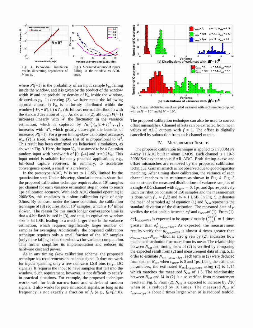
Fig. 5. Measured distribution of sampled variances with each sample computed
with a) 𝑀 = 105 and b) 𝑀 = 104.
The proposed calibration technique can also be used to correct
offset mismatches. Channel offsets can be extracted from mean
values of ADC outputs with f = 1. The offset is digitally
cancelled by subtraction from each channel output.
IV. MEASUREMENT RESULTS
The proposed calibration technique is applied to an 800MS/s
4-way TI ADC built in 40nm CMOS. Each channel is a 10-b
200MS/s asynchronous SAR ADC. Both timing-skew and
offset mismatches are removed by the proposed calibration
technique. Gain mismatch is not observed due to good capacitor
matching. After timing skew calibration, the variance of each
channel reaches to its minimum as shown in Fig. 4. Fig. 5
demonstrates the measured distributions of variance samples of
a single ADC channel with 𝑡𝑠𝑘𝑒𝑤 = 0, 1ps, and 2ps respectively.
Each distribution consists of 150 samples and the measurement
is done with 𝑓𝑖𝑛 ≈ 𝑓𝑠/2 and W ≈ 1 LSB. In Fig. 5, 𝜇 denotes
the mean of sampled 𝜎𝑣2 of equation (1) and 𝑁𝑒𝑠𝑡represents the
standard deviation of the distribution. The measured data of 𝜇
verifies the relationship between 𝜎𝑣2 and 𝑡𝑠𝑘𝑒𝑤of (1). From (1),
𝜎𝑣2|𝑡𝑠𝑘𝑒𝑤=2𝑝𝑠 is expected to be approximately (
2𝑝𝑠
1𝑝𝑠)
2
= 4 times
greater than 𝜎𝑣2|𝑡𝑠𝑘𝑒𝑤=1𝑝𝑠 . As expected, the measurement
results verify that 𝜇𝑡𝑠𝑘𝑒𝑤=2𝑝𝑠 is almost 4 times greater than
𝜇𝑡𝑠𝑘𝑒𝑤=1𝑝𝑠. 𝑁𝑒𝑠𝑡 , which is also given by (2), indicates how
much the distribution fluctuates from its mean. The relationship
between 𝑁𝑒𝑠𝑡 and timing skew of (2) is verified by comparing
the expected result from (2) and measurement data of Fig. 5. In
order to estimate 𝑁𝑒𝑠𝑡|𝑡𝑠𝑘𝑒𝑤=2𝑝𝑠, each term in (2) were deduced
from data of 𝑁𝑒𝑠𝑡 when 𝑡𝑠𝑘𝑒𝑤 is 0 and 1ps. Using the estimated
parameters, the estimated 𝑁𝑒𝑠𝑡|𝑡𝑠𝑘𝑒𝑤=2𝑝𝑠 using (2) is 1.14
which matches the measured 𝑁𝑒𝑠𝑡 of 1.3. The relationship
between 𝑁𝑒𝑠𝑡 and M in (2) is also verified from measurement
results in Fig. 5. From (2), 𝑁𝑒𝑠𝑡 is expected to increase by √10
when M is reduced by 10 times. The measured 𝑁𝑒𝑠𝑡 of
𝑡𝑠𝑘𝑒𝑤=1𝑝𝑠 is about 3 times larger when M is reduced tenfold.
Nu
mb
er
of
Occ
ure
nce
Nu
mb
er
of
Occ
ure
nce
Variance(a) Distributions of variances with M = 5
Variance(b) Distributions of variances with M = 4
Fig. 3. Behavioral simulation
results illustrating dependence of
M on W.
Fig. 4. Measured variance of inputs
falling in the window vs VDL
code.
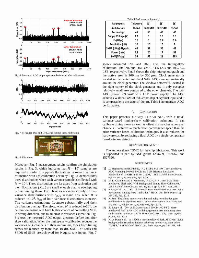
Fig. 6. Measured ADC output spectrum before and after calibration.
Fig. 7. Measured INL and DNL after timing-skew calibration.
Fig. 8. Die photo
Moreover, Fig. 5 measurement results confirm the simulation
results in Fig. 3, which indicates that 𝑀 = 105 samples are
required in order to suppress fluctuations in overall variance
estimation with 1ps calibration accuracy. Fig. 5a demonstrates
three distributions when each variance sample is collected with
𝑀 = 105. Three distributions are far apart from each other and
their fluctuations (𝑁𝑒𝑠𝑡) are small enough that no overlapping
occurs among them. Fig. 5b observes more closely on two
variance distributions with 𝑡𝑠𝑘𝑒𝑤 = 0 and 1ps, when 𝑀 is
reduced to 104. 𝑁𝑒𝑠𝑡 of both variance distributions increase.
The variance estimations fluctuate substantially and their
distribution overlap. Therefore, when 𝑀 is reduced to104, the
calibration engine will have higher chance of controlling VDL
in wrong direction, due to an error in variance estimation. Fig.
6 shows the measured ADC output spectrum before and after
skew calibration. When the timing-skew calibration reduces the
variances of 4 channels to their minimums, tones from timing
skews are reduced by more than 10 dB. SNDR of 48dB and
SFDR of 56dB are achieved for Nyquist rate inputs. Fig. 7
Table I Performance Summary
shows measured INL and DNL after the timing-skew
calibration. The INL and DNL are +1/-1.5 LSB and +0.7/-0.6
LSB, respectively. Fig. 8 shows the chip microphotograph and
the active area is 500 𝜇𝑚 by 300 𝜇𝑚 . Clock generator is
located in the center and the 4 SAR ADCs are symmetrically
around the clock generator. The window detector is located in
the right corner of the clock generator and it only occupies
relatively small area compared to the other channels. The total
ADC power is 9.8mW with 1.1V power supply. The ADC
achieves Walden FoM of 59fJ/conv-step at Nyquist input and it
is comparable to the state-of-the-art. Table I summarizes ADC
performance.
V. CONCLUSION
This paper presents a 4-way TI SAR ADC with a novel
variance-based timing-skew calibration technique. It can
calibrate timing skew as well as offset mismatches among all
channels. It achieves a much faster convergence speed than the
prior variance-based calibration technique. It also reduces the
hardware cost by replacing a flash ADC by a single-comparator
based window detector.
ACKNOWLEDGEMENTS
The authors thank TSMC for the chip fabrication. This work is supported in part by NSF grants 1254459, 1509767, and 1527320.
REFERENCES
[1] D. Stepanovic and B. Nikolic, “A 2.8 GS/s 44.6 mW Time-Interleaved ADC Achieving 50.9 dB SNDR and 3 dB Effective Resolution
Bandwidth of 1.5 GHz in 65 nm CMOS,” IEEE J. Solid-State Circuits,
vol. 48, no. 4, pp. 971-982, Apr. 2013. [2] M. El-Chammas and B. Murmann, “A 12-GS/s 81-mW 5-bit Time-
Interleaved Flash ADC With Background Timing Skew Calibration,”
IEEE J. Solid-State Circuits, vol. 46, no. 4, pp. 838-847, Apr. 2011. [3] S. Lee, et al., “A 1GS/s 10b 18.9mW Time-Interleaved SAR ADC with
Background Timing-Skew Calibration,” ISSCC Dig. Tech. Papers, pp.
384-385, Feb. 2014.
[4] N. Sun, “Exploiting process variation and noise to calibration gain
nonlinearities in pipelined ADCs,” IEEE Transactions on Circuits and
Systems – I, vol. 59, no. 4, pp. 685-695, Apr. 2012. [5] B. Sung et al., “26.4 A 21fJ/conv-step 9 ENOB 1.6GS/S 2× time-
interleaved FATI SAR ADC with background offset and timing-skew
calibration in 45nm CMOS,” in IEEE Conf. ISSCC Dig. Tech. papers, pp.1-3, Feb. 2015
[6] N. Le Dortz et al., “A 1.62GS/s time-interleaved SAR ADC with digital
background mismatch calibration achieving interleaving spurs below 70dBFS,” in IEEE Conf. ISSCC Dig. Tech. papers, pp. 386–388, Feb
2014.
`
After Calibration
SNDR = 48dBSFDR = 56dB
Input Frequency (MHz)
Before CalibrationSNDR = 35dBSFDR = 46dB
Mag
nitu
de (d
B)
Mag
nitu
de (d
B)
`
DN
LIN
L
Digital Code
CLOCKGEN
CH3CH4
CH1CH2
Window Detector
500um
300um
Architecture TI-SAR FATI-SAR FATI-SAR TI-SAR
Technology 45 65 45 40
Supply Voltage (V) 1.1 1 1.1 1.1
Fs (GS/s) 0.8 1 1.6 1.6
Resolution (bit) 10 10 10 9
SNDR (dB) @ Nyquist 48 51 56 48
Power (mW) 9.8 20 17 93
FoM(fJ/step) 59 62 21 283
This workParameters [3] [5] [6]


![FOR A 10-BIT 12 GS/s 16-CHANNEL TIME …References [1] C. C. Hsu, F. C. Huang et al., “An 11b 800MS/s time-interleaved ADC with digital background calibration,” in 2007 IEEE ISSCC](https://img.pdfslide.net/doc/110x75/5f5f70aebaa50915b917e25a/for-a-10-bit-12-gss-16-channel-time-references-1-c-c-hsu-f-c-huang-et-al.jpg)