Embed Size (px)
DESCRIPTION
A General Purpose Charge Readout Chip for TPC Applications Munich, 19 October 2006 Luciano Musa Gerd Trampitsch. OUTLINE. R&D on the readout electronics for the LC TPC Alice TPC Readout - MWPC General Purpose Charge Readout Chip Prototype Submission of the Analog Front End - PowerPoint PPT Presentation
Citation preview
1Luciano Musa, Gerd Trampitsch
A General Purpose Charge Readout Chip
for TPC Applications
Munich, 19 October 2006
Luciano Musa
Gerd Trampitsch
2Luciano Musa, Gerd Trampitsch
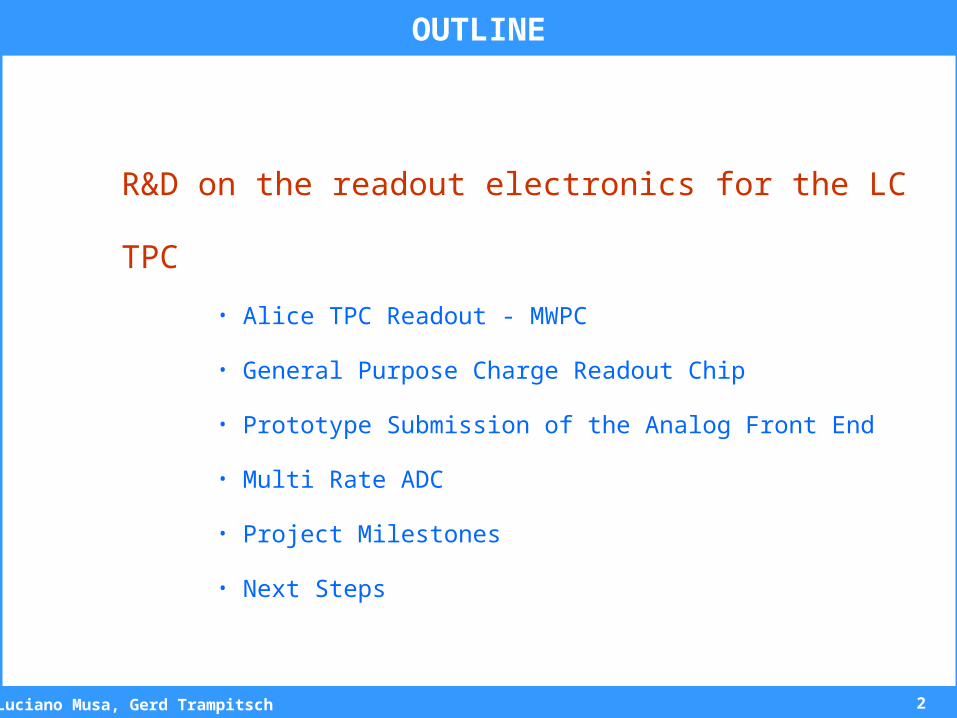
R&D on the readout electronics for the LC TPC
• Alice TPC Readout - MWPC
• General Purpose Charge Readout Chip
• Prototype Submission of the Analog Front End
• Multi Rate ADC
• Project Milestones
• Next Steps
OUTLINE
3Luciano Musa, Gerd Trampitsch
anode wire
pad plane
drift region88s
L1: 5s 200 Hz
PASA ADC DigitalCircuit
RAM
8 CHIPS x
16 CH / CHIP
8 CHIPSx
16 CH / CHIP
CUSTOM IC(CMOS 0.35m) CUSTOM IC (CMOS 0.25m )
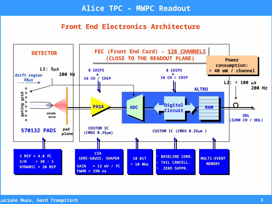
DETECTOR FEC (Front End Card) - 128 CHANNELS(CLOSE TO THE READOUT PLANE)
FEC (Front End Card) - 128 CHANNELS(CLOSE TO THE READOUT PLANE)
570132 PADS
1 MIP = 4.8 fC
S/N = 30 : 1
DYNAMIC = 30 MIP
CSA SEMI-GAUSS. SHAPER
GAIN = 12 mV / fCFWHM = 190 ns
10 BIT
< 10 MHz
• BASELINE CORR.
• TAIL CANCELL.
• ZERO SUPPR.
MULTI-EVENT
MEMORY
L2: < 100 s 200 Hz
DDL(3200 CH / DDL)
Powerconsumption:
< 40 mW / channel
Powerconsumption:
< 40 mW / channel
gat
ing
gri
d
ALTRO
Front End Electronics Architecture
Alice TPC – MWPC Readout
4Luciano Musa, Gerd Trampitsch
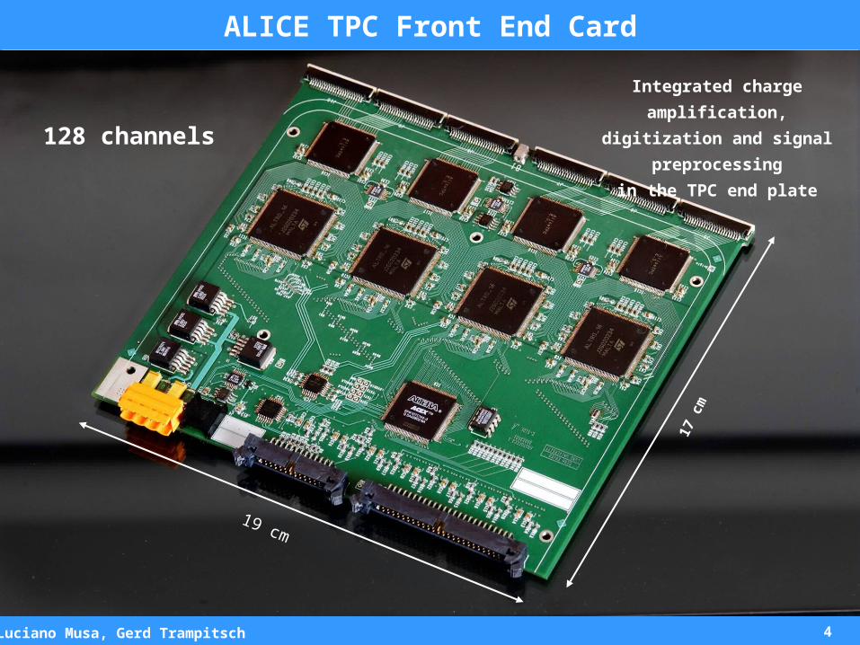
19 cm
17 c
m
ALICE TPC Front End Card
Integrated charge amplification,
digitization and signal
preprocessing
in the TPC end plate
128 channels
5Luciano Musa, Gerd Trampitsch
Motivations & Specifications 1/2
• Requirements of the front-end and readout electronics for High Energy Physics Experiments:
low power, high speed, high density, low mass, radiation tolerance
• These requirements can only be met by highly integrated systems implemented with very deep submicron CMOS technologies.
• The volumes of ICs required for a typical HEP detector remain low <1Mch
• Non Recursive Engineering (NRE) costs are more and more dominant for high energy physics.
• Development of standard chips capable of handling a wide range of high
energy physics applications, in order to warrant the NRE expenditure.
• Likely this polyvalence will be obtained through an increased level of programmability.
6Luciano Musa, Gerd Trampitsch
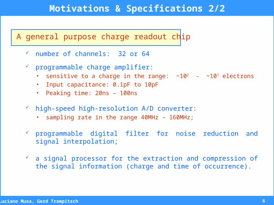
A general purpose charge readout chip
number of channels: 32 or 64
programmable charge amplifier: • sensitive to a charge in the range: ~102 - ~107 electrons • Input capacitance: 0.1pF to 10pF • Peaking time: 20ns – 100ns
high-speed high-resolution A/D converter: • sampling rate in the range 40MHz - 160MHz;
programmable digital filter for noise reduction and signal interpolation;
a signal processor for the extraction and compression of the signal information (charge and time of occurrence).
Motivations & Specifications 2/2
7Luciano Musa, Gerd Trampitsch
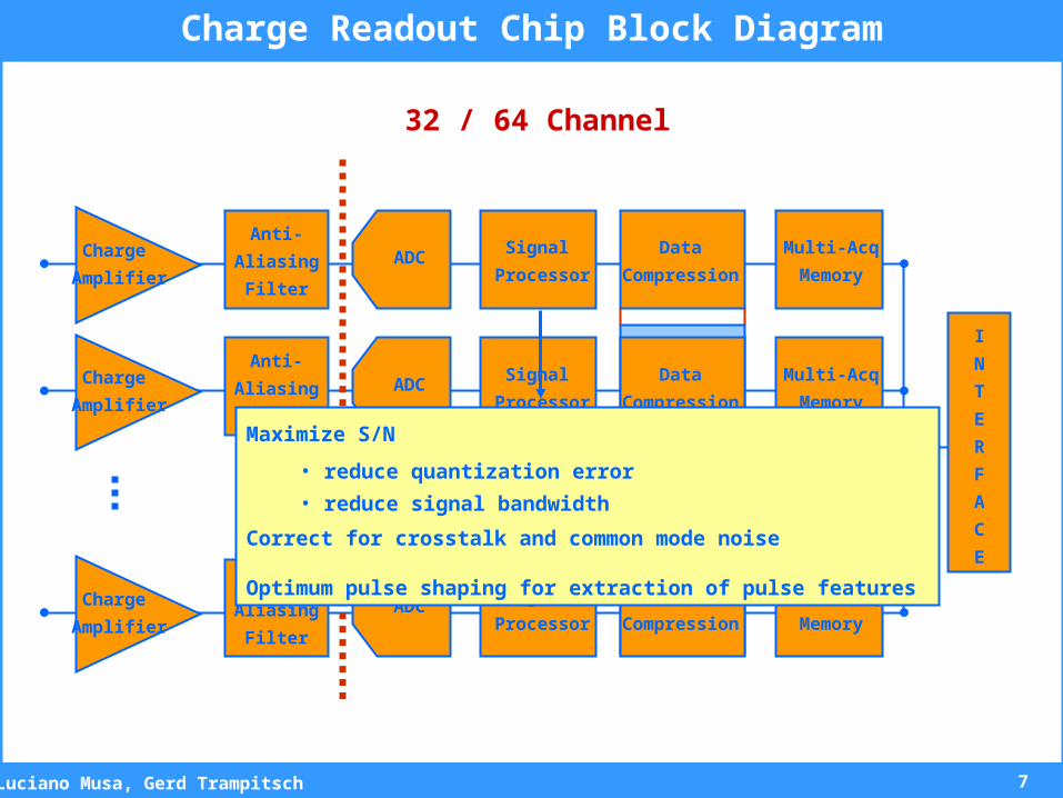
Charge Readout Chip Block Diagram
32 / 64 Channel
Charge
Amplifier
Anti-
Aliasing
Filter
ADCSignal
Processor
Data
Compression
Multi-Acq
Memory
Hit Finder
Feature
Extaction
Histogrammer
Charge
Amplifier
Anti-
Aliasing
Filter
ADCSignal
Processor
Data
Compression
Multi-Acq
Memory
Charge
Amplifier
Anti-
Aliasing
Filter
ADCSignal
Processor
Data
Compression
Multi-Acq
Memory
I
N
T
E
R
F
A
C
E
Maximize S/N
• reduce quantization error
• reduce signal bandwidth
Correct for crosstalk and common mode noise
Optimum pulse shaping for extraction of pulse features
8Luciano Musa, Gerd Trampitsch
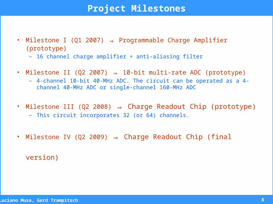
• Milestone I (Q1 2007) Programmable Charge Amplifier (prototype)⇒– 16 channel charge amplifier + anti-aliasing filter
• Milestone II (Q2 2007) 10-bit multi-rate ADC (prototype)⇒– 4-channel 10-bit 40-MHz ADC. The circuit can be operated as a 4-channel 40-
MHz ADC or single-channel 160-MHz ADC
• Milestone III (Q2 2008) Charge Readout Chip (prototype)⇒– This circuit incorporates 32 (or 64) channels.
• Milestone IV (Q2 2009) Charge Readout Chip (final version)⇒
Project Milestones
9Luciano Musa, Gerd Trampitsch
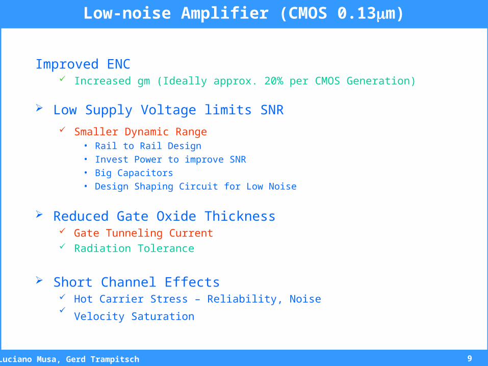
Low-noise Amplifier (CMOS 0.13m)
Improved ENC Increased gm (Ideally approx. 20% per CMOS Generation)
Low Supply Voltage limits SNR
Smaller Dynamic Range• Rail to Rail Design
• Invest Power to improve SNR
• Big Capacitors
• Design Shaping Circuit for Low Noise
Reduced Gate Oxide Thickness Gate Tunneling Current Radiation Tolerance
Short Channel Effects Hot Carrier Stress – Reliability, Noise
Velocity Saturation
10Luciano Musa, Gerd Trampitsch
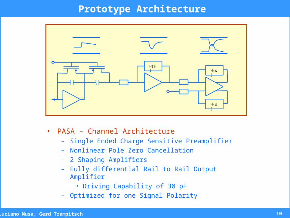
Prototype Architecture
• PASA – Channel Architecture– Single Ended Charge Sensitive Preamplifier– Nonlinear Pole Zero Cancellation– 2 Shaping Amplifiers– Fully differential Rail to Rail Output Amplifier
• Driving Capability of 30 pF– Optimized for one Signal Polarity
H(s)H(s)
H(s)
11Luciano Musa, Gerd Trampitsch
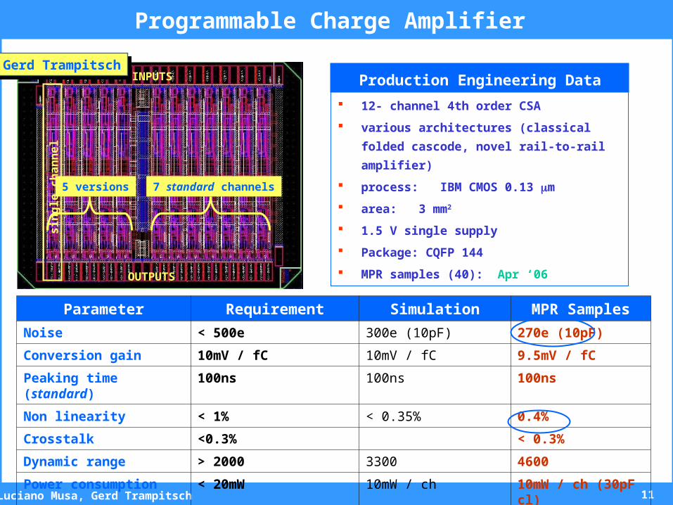
Programmable Charge Amplifier
12- channel 4th order CSA
various architectures (classical folded
cascode, novel rail-to-rail amplifier)
process: IBM CMOS 0.13 m
area: 3 mm2
1.5 V single supply
Package: CQFP 144
MPR samples (40): Apr ‘06
Production Engineering Data
Parameter Requirement Simulation MPR Samples
Noise < 500e 300e (10pF) 270e (10pF)
Conversion gain 10mV / fC 10mV / fC 9.5mV / fC
Peaking time (standard) 100ns 100ns 100ns
Non linearity < 1% < 0.35% 0.4%
Crosstalk <0.3% < 0.3%
Dynamic range > 2000 3300 4600
Power consumption < 20mW 10mW / ch 10mW / ch (30pF cl)
OUTPUTS
INPUTS
sin
gle
ch
an
ne
l
7 standard channels5 versions
Gerd TrampitschGerd Trampitsch
12Luciano Musa, Gerd Trampitsch
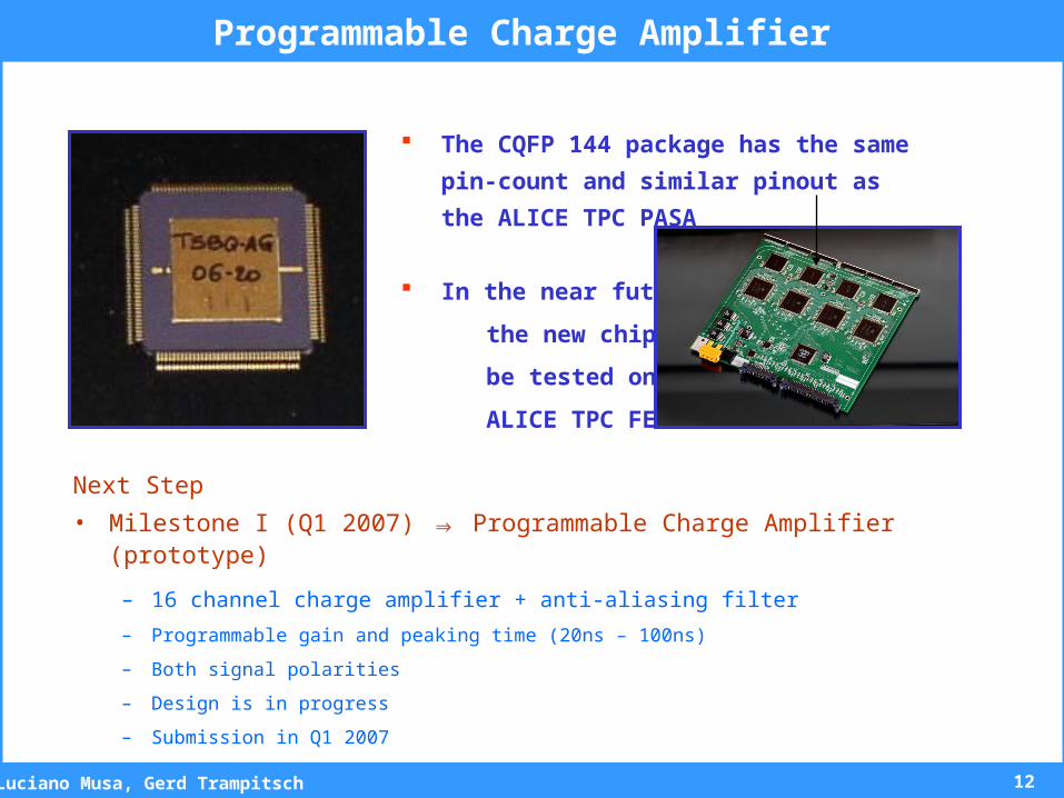
Programmable Charge Amplifier
The CQFP 144 package has the same pin-
count and similar pinout as the ALICE
TPC PASA
In the near future
the new chip will
be tested on a
ALICE TPC FEC
Next Step
• Milestone I (Q1 2007) Programmable Charge Amplifier (prototype)⇒
– 16 channel charge amplifier + anti-aliasing filter
– Programmable gain and peaking time (20ns – 100ns)
– Both signal polarities
– Design is in progress
– Submission in Q1 2007
13Luciano Musa, Gerd Trampitsch
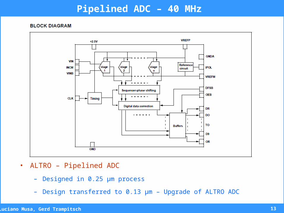
Pipelined ADC – 40 MHz
• ALTRO – Pipelined ADC
– Designed in 0.25 μm process
– Design transferred to 0.13 μm – Upgrade of ALTRO ADC
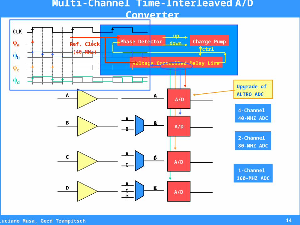
14Luciano Musa, Gerd Trampitsch
Phase Detector Charge Pump
Voltage Controlled Delay Line
up
downVctrl
Ref. Clock
(40 MHz)
C
B
A
D
A/DA/D
A/D
A/D
A/D
Multi-Channel Time-Interleaved A/D Converter
A
B
A
C
ACD
Upgrade of
ALTRO ADC
4-Channel
40-MHZ ADC
A
B
C
D
2-Channel
80-MHZ ADC
C
A
A
C
1-Channel
160-MHZ ADC
A
A
A
A
a
b
c
d
CLK
a
b
c
d
CLK
a
b
c
d
CLK
15Luciano Musa, Gerd Trampitsch
• The development of a general purpose charge readout chip has started. This chip incorporates:
– Programmable analogue front end– Multi-rate Analogue to Digital Converter– General purpose signal processor
• First prototype of the shaping amplifier in CMOS 0.13 μm– Submitted in December 2005– 40 samples of the MPWR successfully characterized in 2006– All circuit parameters meet the design specifications– The design and layout of a programmable gain and bandwidth amplifier is
currently in progress and will be finished early next year
• Time interleaved Multi-Rate ADC– The basic building block was transferred to IBM 0.13 μm– Design is still in progress
Summary