Embed Size (px)
Citation preview
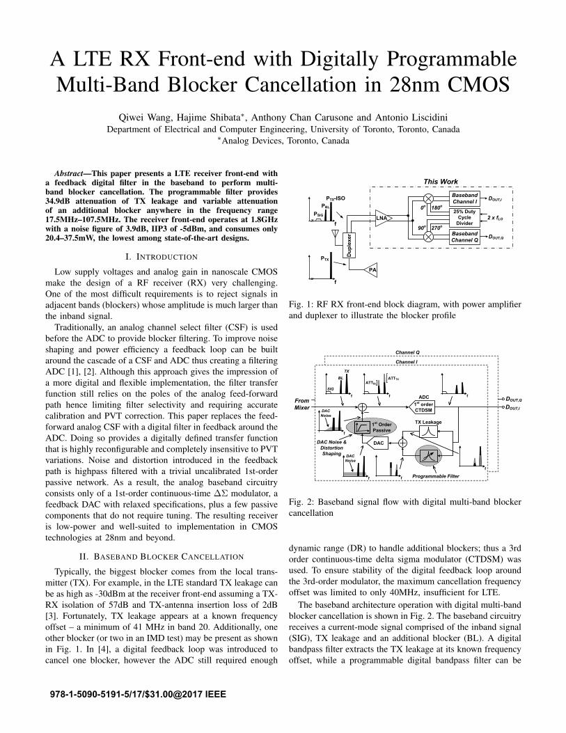
A LTE RX Front-end with Digitally ProgrammableMulti-Band Blocker Cancellation in 28nm CMOS
Qiwei Wang, Hajime Shibata∗, Anthony Chan Carusone and Antonio LiscidiniDepartment of Electrical and Computer Engineering, University of Toronto, Toronto, Canada
∗Analog Devices, Toronto, Canada
Abstract—This paper presents a LTE receiver front-end witha feedback digital filter in the baseband to perform multi-band blocker cancellation. The programmable filter provides34.9dB attenuation of TX leakage and variable attenuationof an additional blocker anywhere in the frequency range17.5MHz–107.5MHz. The receiver front-end operates at 1.8GHzwith a noise figure of 3.9dB, IIP3 of -5dBm, and consumes only20.4–37.5mW, the lowest among state-of-the-art designs.
I. INTRODUCTION
Low supply voltages and analog gain in nanoscale CMOSmake the design of a RF receiver (RX) very challenging.One of the most difficult requirements is to reject signals inadjacent bands (blockers) whose amplitude is much larger thanthe inband signal.
Traditionally, an analog channel select filter (CSF) is usedbefore the ADC to provide blocker filtering. To improve noiseshaping and power efficiency a feedback loop can be builtaround the cascade of a CSF and ADC thus creating a filteringADC [1], [2]. Although this approach gives the impression ofa more digital and flexible implementation, the filter transferfunction still relies on the poles of the analog feed-forwardpath hence limiting filter selectivity and requiring accuratecalibration and PVT correction. This paper replaces the feed-forward analog CSF with a digital filter in feedback around theADC. Doing so provides a digitally defined transfer functionthat is highly reconfigurable and completely insensitive to PVTvariations. Noise and distortion introduced in the feedbackpath is highpass filtered with a trivial uncalibrated 1st-orderpassive network. As a result, the analog baseband circuitryconsists only of a 1st-order continuous-time ∆Σ modulator, afeedback DAC with relaxed specifications, plus a few passivecomponents that do not require tuning. The resulting receiveris low-power and well-suited to implementation in CMOStechnologies at 28nm and beyond.
II. BASEBAND BLOCKER CANCELLATION
Typically, the biggest blocker comes from the local trans-mitter (TX). For example, in the LTE standard TX leakage canbe as high as -30dBm at the receiver front-end assuming a TX-RX isolation of 57dB and TX-antenna insertion loss of 2dB[3]. Fortunately, TX leakage appears at a known frequencyoffset – a minimum of 41 MHz in band 20. Additionally, oneother blocker (or two in an IMD test) may be present as shownin Fig. 1. In [4], a digital feedback loop was introduced tocancel one blocker, however the ADC still required enough
PTX-ISO
f
PBL
PSIG
Du
ple
xe
r
PA
LNA
25% Duty
Cycle
Divider
0o
180o
270o
90o
2 x fLO
Baseband
Channel I
Baseband
Channel Q
DOUT,I
DOUT,Q
PTX
f
This Work
Fig. 1: RF RX front-end block diagram, with power amplifierand duplexer to illustrate the blocker profile
TX Leakage
DAC
DOUT,I
f
ATTTX
ATTBL
f
TX
BL
SIG
f
DAC
Noise
f
DAC
Noise
f
f
f
From
Mixer
DOUT,Q
Channel I
Channel Q
ADC
1st
order
CTDSM
1st
Order
Passive
DAC Noise &
Distortion
Shaping
Programmable Filter
Fig. 2: Baseband signal flow with digital multi-band blockercancellation
dynamic range (DR) to handle additional blockers; thus a 3rdorder continuous-time delta sigma modulator (CTDSM) wasused. To ensure stability of the digital feedback loop aroundthe 3rd-order modulator, the maximum cancellation frequencyoffset was limited to only 40MHz, insufficient for LTE.
The baseband architecture operation with digital multi-bandblocker cancellation is shown in Fig. 2. The baseband circuitryreceives a current-mode signal comprised of the inband signal(SIG), TX leakage and an additional blocker (BL). A digitalbandpass filter extracts the TX leakage at its known frequencyoffset, while a programmable digital bandpass filter can be
978-1-5090-5191-5/17/$31.00@2017 IEEE
32
IIN,I
VCM
DOUT,I
DAC1
B2T
T2B
NLDACDIG
16
Digital @ 720MHz
C0=80pF
R0=100Ω
C1=690fF
R1=400Ω
C2=150fF
R2=2kΩ
R22=8kΩ 17 level
Quantizer
@ 720MHz
CDAC=17pF
RDAC=460Ω
+_
Channel I
Channel Q
IIN,Q+_ DOUT,Q
VIN+ VIN−
VIN+ VIN−VIN+ VIN−
VOUT+
VOUT−
VCM1
VBN1
VBP2
VCM2 VCM3
VBP3
1.6mA 0.8mA 0.6mA
TX Leakage
Programmable
DA
C2
5
HPF for
Noise and
Distortion
Shaping
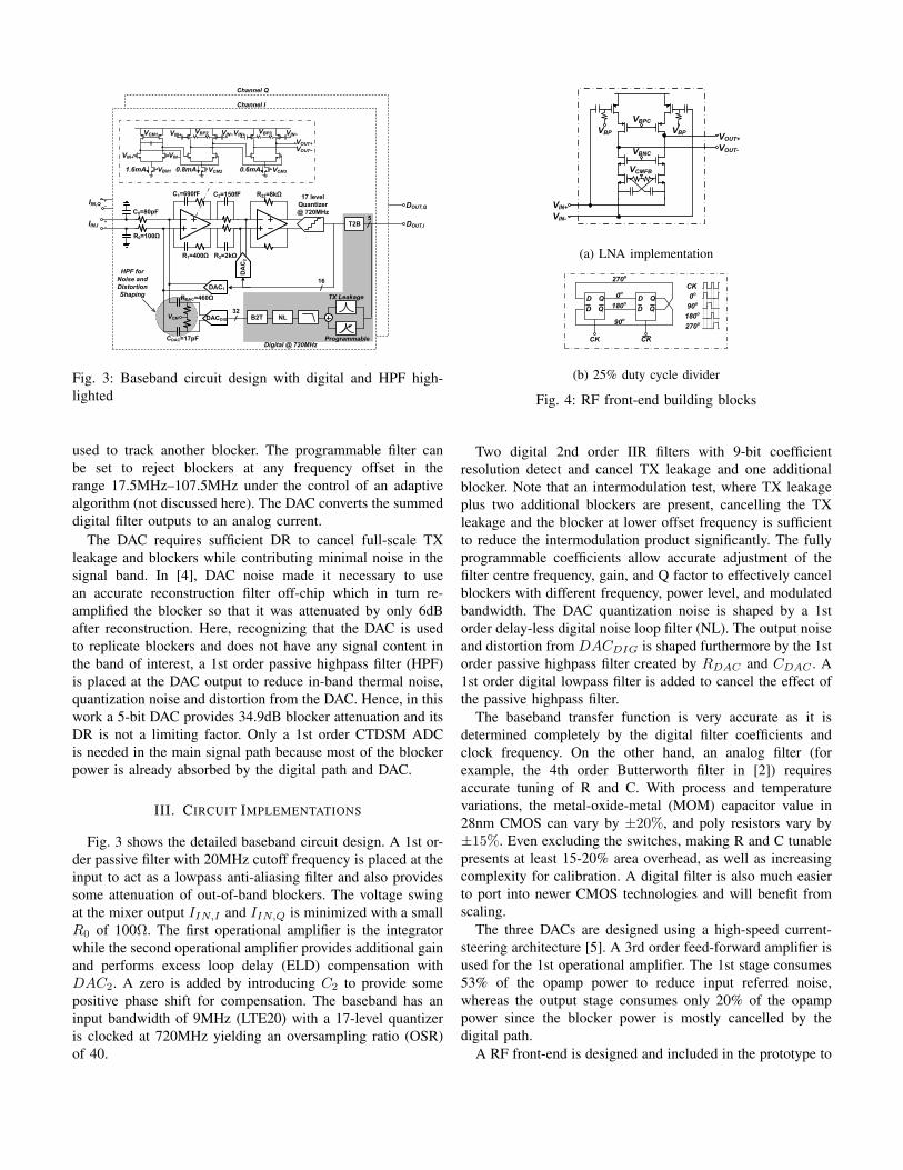
Fig. 3: Baseband circuit design with digital and HPF high-lighted
used to track another blocker. The programmable filter canbe set to reject blockers at any frequency offset in therange 17.5MHz–107.5MHz under the control of an adaptivealgorithm (not discussed here). The DAC converts the summeddigital filter outputs to an analog current.
The DAC requires sufficient DR to cancel full-scale TXleakage and blockers while contributing minimal noise in thesignal band. In [4], DAC noise made it necessary to usean accurate reconstruction filter off-chip which in turn re-amplified the blocker so that it was attenuated by only 6dBafter reconstruction. Here, recognizing that the DAC is usedto replicate blockers and does not have any signal content inthe band of interest, a 1st order passive highpass filter (HPF)is placed at the DAC output to reduce in-band thermal noise,quantization noise and distortion from the DAC. Hence, in thiswork a 5-bit DAC provides 34.9dB blocker attenuation and itsDR is not a limiting factor. Only a 1st order CTDSM ADCis needed in the main signal path because most of the blockerpower is already absorbed by the digital path and DAC.
III. CIRCUIT IMPLEMENTATIONS
Fig. 3 shows the detailed baseband circuit design. A 1st or-der passive filter with 20MHz cutoff frequency is placed at theinput to act as a lowpass anti-aliasing filter and also providessome attenuation of out-of-band blockers. The voltage swingat the mixer output IIN,I and IIN,Q is minimized with a smallR0 of 100Ω. The first operational amplifier is the integratorwhile the second operational amplifier provides additional gainand performs excess loop delay (ELD) compensation withDAC2. A zero is added by introducing C2 to provide somepositive phase shift for compensation. The baseband has aninput bandwidth of 9MHz (LTE20) with a 17-level quantizeris clocked at 720MHz yielding an oversampling ratio (OSR)of 40.
VIN+
VCMFB
VBPC
VBPVBP
VIN-
VBNC
VOUT+
VOUT-
(a) LNA implementation
D
D
Q
Q
CK
D
D
Q
Q
CK
0o
180o
270o
90o
CK
0o
180o
270o
90o
(b) 25% duty cycle divider
Fig. 4: RF front-end building blocks
Two digital 2nd order IIR filters with 9-bit coefficientresolution detect and cancel TX leakage and one additionalblocker. Note that an intermodulation test, where TX leakageplus two additional blockers are present, cancelling the TXleakage and the blocker at lower offset frequency is sufficientto reduce the intermodulation product significantly. The fullyprogrammable coefficients allow accurate adjustment of thefilter centre frequency, gain, and Q factor to effectively cancelblockers with different frequency, power level, and modulatedbandwidth. The DAC quantization noise is shaped by a 1storder delay-less digital noise loop filter (NL). The output noiseand distortion from DACDIG is shaped furthermore by the 1storder passive highpass filter created by RDAC and CDAC . A1st order digital lowpass filter is added to cancel the effect ofthe passive highpass filter.
The baseband transfer function is very accurate as it isdetermined completely by the digital filter coefficients andclock frequency. On the other hand, an analog filter (forexample, the 4th order Butterworth filter in [2]) requiresaccurate tuning of R and C. With process and temperaturevariations, the metal-oxide-metal (MOM) capacitor value in28nm CMOS can vary by ±20%, and poly resistors vary by±15%. Even excluding the switches, making R and C tunablepresents at least 15-20% area overhead, as well as increasingcomplexity for calibration. A digital filter is also much easierto port into newer CMOS technologies and will benefit fromscaling.
The three DACs are designed using a high-speed current-steering architecture [5]. A 3rd order feed-forward amplifier isused for the 1st operational amplifier. The 1st stage consumes53% of the opamp power to reduce input referred noise,whereas the output stage consumes only 20% of the opamppower since the blocker power is mostly cancelled by thedigital path.
A RF front-end is designed and included in the prototype to
LNA
Mixer & Divider
Channel I
1.38mm
1.07
mm
AMP1
AMP2DAC2
FlashDigitalDACDIG
HPF
DAC1
Channel Q
Fig. 5: Die photo.
TABLE I: Measurement summary and comparison table withother DSM-based receivers.
[2] [7] [8] [9]
RX with ∆Σ-CSFRX with
filtering ADCDirect ∆Σ RX
Direct
∆Σ RX
65 80 65 40
0.6-3 0.04-1 0.4-4 0.7-2.7 0.9 1.8
2.4-3.5 2.7-3.5 16 5.9-8.8 3.8 3.9
RF3 23.5-36.7 113.4 - 48 4.4 5.3
BB Analog 12-16.3 108 - 42 14.6 14.6
BB Digital - - - 0.5-17.6 0.5-17.6
1.2 1.8/1 1.5/1.2 1.1
-6 -13 13.5 -2 -7 -5
45-52 52-68 40-43
10,20,40 5,6,7,8 4,10 1.4,15
0.7 5.64 0.56 1
1. LTE20 mode 2. Estimated 3. RF power includes LNA, mixer, LO gen and distribution
4. Incl. PLL and DSP
RF Carrier BW (MHz) 18
Area (mm2) 0.64
20.4-37.5
Supply (V) 0.9
IIP3 (dBm)
SNDR (dB) 48
19.5-36.6
Power
Breakdown
(mW)
35.5-53
17-70.5
RF Frequency (GHz)
NF(dB)
Power (mW) 221.4 90
This work
Architecture RX with ∆Σ-fb
digital filter
CMOS Technology (nm) 28
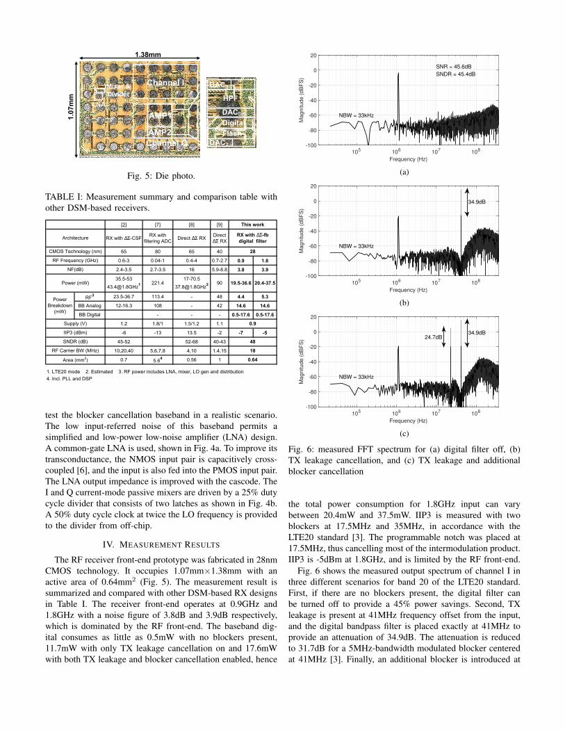
test the blocker cancellation baseband in a realistic scenario.The low input-referred noise of this baseband permits asimplified and low-power low-noise amplifier (LNA) design.A common-gate LNA is used, shown in Fig. 4a. To improve itstransconductance, the NMOS input pair is capacitively cross-coupled [6], and the input is also fed into the PMOS input pair.The LNA output impedance is improved with the cascode. TheI and Q current-mode passive mixers are driven by a 25% dutycycle divider that consists of two latches as shown in Fig. 4b.A 50% duty cycle clock at twice the LO frequency is providedto the divider from off-chip.
IV. MEASUREMENT RESULTS
The RF receiver front-end prototype was fabricated in 28nmCMOS technology. It occupies 1.07mm×1.38mm with anactive area of 0.64mm2 (Fig. 5). The measurement result issummarized and compared with other DSM-based RX designsin Table I. The receiver front-end operates at 0.9GHz and1.8GHz with a noise figure of 3.8dB and 3.9dB respectively,which is dominated by the RF front-end. The baseband dig-ital consumes as little as 0.5mW with no blockers present,11.7mW with only TX leakage cancellation on and 17.6mWwith both TX leakage and blocker cancellation enabled, hence
Frequency (Hz)
105 106 107 108
Ma
gn
itu
de
(d
BF
S)
-100
-80
-60
-40
-20
0
20
SNR = 45.6dB
SNDR = 45.4dB
NBW = 33kHz
(a)
Frequency (Hz)
105 106 107 108
Ma
gn
itu
de
(d
BF
S)
-100
-80
-60
-40
-20
0
20
34.9dB
NBW = 33kHz
(b)
Frequency (Hz)
105 106 107 108
Ma
gn
itu
de
(d
BF
S)
-100
-80
-60
-40
-20
0
20
34.9dB 24.7dB
NBW = 33kHz
(c)
Fig. 6: measured FFT spectrum for (a) digital filter off, (b)TX leakage cancellation, and (c) TX leakage and additionalblocker cancellation
the total power consumption for 1.8GHz input can varybetween 20.4mW and 37.5mW. IIP3 is measured with twoblockers at 17.5MHz and 35MHz, in accordance with theLTE20 standard [3]. The programmable notch was placed at17.5MHz, thus cancelling most of the intermodulation product.IIP3 is -5dBm at 1.8GHz, and is limited by the RF front-end.
Fig. 6 shows the measured output spectrum of channel I inthree different scenarios for band 20 of the LTE20 standard.First, if there are no blockers present, the digital filter canbe turned off to provide a 45% power savings. Second, TXleakage is present at 41MHz frequency offset from the input,and the digital bandpass filter is placed exactly at 41MHz toprovide an attenuation of 34.9dB. The attenuation is reducedto 31.7dB for a 5MHz-bandwidth modulated blocker centeredat 41MHz [3]. Finally, an additional blocker is introduced at
Input Offset Frequency(MHz)
0 20 40 60 80 100
Ga
in (
dB
)
-40
-30
-20
-10
0
TX notch
Programmable notch frequency range
(a)
Input Offset Frequency(MHz)
0 20 40 60 80 100
Ga
in (
dB
)
-40
-30
-20
-10
0
TX notch
Attenuation
Range
Attenuation setting = 3
Attenuation setting = 2
Attenuation setting = 1
(b)
Input Offset Frequency(MHz)
0 20 40 60 80 100
Ga
in (
dB
)
-40
-30
-20
-10
0
TX notch
Programmable
Q factorQ = 24
Q = 12
Q = 6
(c)
Fig. 7: Measured baseband frequency response for pro-grammable notch at different (a) frequency, (b) attenuation,and (c) Q factor settings
22.5MHz and is attenuated by 24.7dB by the programmablefilter. The grey lines in the FFT spectrum are only used toillustrate the amount of attenuation.
Fig. 7 shows the measured baseband frequency responsewith different settings for the programmable notch. Itcan be moved to any precise frequency in the range of17.5MHz–107.5MHz. The amount of attenuation can be de-creased to increase the loop phase margin. In addition, the Qfactor of the notch can be adjusted depending on the modulatedblocker bandwidth. A low Q notch is undesirable near thesignal band to prevent signal attenuation, however that’s not aproblem as blockers close to the signal band have a maximumbandwidth of 5MHz [3].
Signal to noise and distortion ratio (SNDR) is measuredwith a signal input offset 1MHz from the carrier, and the
Input Power (dBm)
-100 -90 -80 -70 -60 -50 -40 -30 -20
SN
DR
/IN
DR
(d
B)
0
20
40
60
80
24dB
SNDR/INDR versus RF Input Power
SNDR (@1MHz offset)
INDR (@41MHz offset)
Fig. 8: SNDR and INDR versus RF input power.
interference-to-noise and distortion ratio (INDR) is measuredat 41MHz offset, as shown in Fig. 8. It can be seen that thereceiver front-end can handle a TX leakage 24dB larger thanthe ADC fullscale, while maintaining the same in-band noise.
V. CONCLUSION
A RF receiver with a multi-blocker cancelling baseband isintroduced as a replacement for the conventional cascade ofanalog filter and ADC. The digital bandpass filters producetwo flexible notches in the baseband frequency response,cancelling TX leakage and an additional blocker as required bythe LTE20 standard. Compared with previous state-of-the-artdesigns, this work achieves competitive IIP3 and noise figure,while consuming the lowest power and can dynamically scaleits power depending on the number of blockers present.
ACKNOWLEDGMENT
The authors would like to acknowledge Analog Devicesfor financial support, fabricating and packaging the chip, andprovision of test equipments.
REFERENCES
[1] M. Sosio, A. Liscidini, R. Castello, and F. De Bernardinis, “A completeDVB-T/ATSC tuner analog base-band implemented with a single filteringADC,” Proc. IEEE ESSCIRC, 2011, pp. 391–394.
[2] X. Liu et al., “A 65 nm CMOS Wideband Radio Receiver With ∆Σ-BasedA/D-Converting Channel-Select Filters,” IEEE J. Solid-State Circuits,vol. 51, no. 7, pp. 1566–1578, Jul. 2016.
[3] User Equipment (UE) radio transmission and reception (Release 11),3GPP TS 36.101 V11.6.0 (2013-10)
[4] R. Ritter, J. G. Kauffman, J. Becker, and M. Ortmanns, “A 10 MHzBandwidth, 70dB SNDR Continuous Time Delta-Sigma Modulator WithDigitally Improved Reconfigurable Blocker Rejection,” IEEE J. Solid-State Circuits, vol. 51, no. 3, pp. 660–670, Mar. 2016.
[5] Y. Dong et al., “A 930mW 69dB-DR 465MHz-BW CT 1-2 MASH ADCin 28nm CMOS,” ISSCC Dig. Tech. Papers, vol. 51, no. 3, pp. 278–279,Feb. 2016.
[6] X. Li, S. Shekhar and D. J. Allstot, “Gm-Boosted Common-Gate LNAand Differential Colpitts VCO/QVCO in 0.18-um CMOS,” IEEE J. Solid-State Circuits, vol. 40, no. 12, pp. 2609–2619, Dec. 2005.
[7] J. Greenberg et al., “A 40-MHz-to-1-GHz Fully Integrated MultistandardSilicon Tuner in 80-nm CMOS,” IEEE J. Solid-State Circuits, vol. 48,no. 11, pp. 2746–2761, Nov. 2013.
[8] C. Wu, E. Alon, and B. Nikolic, “A Wideband 400 MHz-to-4 GHz DirectRF-to-Digital Multimode ∆Σ Receiver,” IEEE J. Solid-State Circuits, vol.49, no. 7, pp. 1639–1652, Jul. 2014.
[9] M. Englund et al., “A Programmable 0.7-2.7 GHz Direct ∆Σ Receiver in40 nm CMOS,” IEEE J. Solid-State Circuits, vol. 50, no. 3, pp. 644–655,Mar. 2015.


![Programmable System-on-Chip (PSoC20 to 24 programmable logic device (PLD) based universal digital blocks (UDBs) Full CAN 2.0b 16 RX, 8 TX buffers[2] Full-Speed (FS) USB 2.0 12 Mbps](https://img.pdfslide.net/doc/110x75/5f868ee9e095d26609636ae2/programmable-system-on-chip-psoc-20-to-24-programmable-logic-device-pld-based.jpg)