Embed Size (px)
Citation preview
8/8/2019 A NOVEL WIDE BAND YAGI-UDA ANTENNA
http://slidepdf.com/reader/full/a-novel-wide-band-yagi-uda-antenna 1/18
Progress In Electromagnetics Research B, Vol. 16, 389–406, 2009
A NOVEL WIDE-BAND MICROSTRIP YAGI-UDAARRAY ANTENNA FOR WLAN APPLICATIONS
M. Bemani and S. Nikmehr
Faculty of Electrical EngineeringUniversity of Tabriz
Tabriz, Iran
Abstract—This paper presents a design of Wide-Band MicrostripYagi-Uda antenna with high gain and high front to back (F/B)ratio. Numerical and measured results of our design show more than18 dB front to back ratio at 5.5 GHz and no backward radiation at5.2 GHz. An impedance bandwidth of 22.05% was achieved around5.5 GHz. The antenna gain (10–12.4 dBi) can be varied to be suitablefor various applications. Measured return loss and radiation patternof this antenna is presented to validate the results of simulationsby two methods. The first method based on finite element method(FEM) and the second one based on finite integral technique (FIT)were used to analyze antenna structure, and subsequently the GeneticAlgorithm (GA) was applied by using HFSS simulator to obtain theoptimized parameters. In order to find the best design method forthis antenna, the effect of distance between the parasitic elementsof proposed antenna was studied. Finally two microstrip Yagi-Udaarray antennas were combined to increase the gain of antenna. Todemonstrate the major benefits, a comparison of our initial and final
designs of Yagi-Uda antenna is provided.
1. INTRODUCTION
These days numerous research activities are being pursued on thesubject of wireless communications, which use the microwave ormillimeter band [1, 2]. We have witnessed a tremendous growthof wireless communication links in recent years. Most wireless
networks use omni-directional antennas [3]. However, in someapplications we need directional antennas such as Log Periodic and
Corresponding author: M. Bemani ([email protected]).

8/8/2019 A NOVEL WIDE BAND YAGI-UDA ANTENNA
http://slidepdf.com/reader/full/a-novel-wide-band-yagi-uda-antenna 2/18
390 Bemani and Nikmehr
Yagi-Uda antennas [4–7]. These types of antennas find their usein many applications such as industrial, medical, radar and wireless
communications. The microstrip Yagi-Uda array consists of a drivenmicrostrip antenna along with several parasitic microstrip antennaswhich are arranged on the same substrate surface in a way that theoverall antenna characteristics are enhanced [8]. It is clear that inarray applications, the effect of mutual coupling is usually undesirable,because it reduces the antenna gain, raises the side lobe level, etc.However, in some applications mutual coupling enhances the antennaperformance. For example, in the case of microstrip antenna, parasiticpatches can be placed around a driven element to increase the gain of this single driven element by several decibels [9]. Also, it is interestingthat parasitic patches with open circuit stubs can shape the beam of antenna so that it is tilted in a desired direction [10].
The first researcher who suggested the use of Yagi-Uda antennadesign in microstrip structures was Huang in 1989 [11]. His proposedantenna consisted of four patches that were electromagneticallycoupled to each other. That antenna had maximum gain of 8 dBiand low F/B ratio. After that, Huang and Densmor introduced anew microstrip Yagi-Uda antenna that had a maximum gain of 14 dBibut its use in some applications was problematic because of its low
F/B ratio. The large size of this antenna was also the source of otherdifficulties [12]. Later, many methods were proposed to improve thegain and F/B ratio of these antennas, such as using a periodic band-gap(PBG) structure [13]. These periodic structures affect the transmissionof propagating waves. Proper utilization of PBGs has potential toimprove performances of radiating elements [14–17].
In [18], a new type of microstrip Yagi-Uda antenna was introducedwhich achieved high gain and high F/B ratio. However, this antennawas single band, working at 5.2 GHz with return loss of 15 dB at thisfrequency.
In this paper, we present a novel design of broad band microstripYagi-Uda antenna which supports 5.2 and 5.8 GHz bands. Ourproposed antenna is designed to operate around the 5.5 GHz band,which is used in recent wireless local-area networks (LANs) and isbeing considered for next-generation mobile communications.
Although the proposed antenna can be scaled to be used at muchhigher frequencies, such as 34 GHz, this paper discusses only 5.5 GHzband operation since we try to confirm the basic performance of ourantenna with little manufacturing error.
The proposed antenna configuration has high gain and high F/Bratio, and the return loss in both bands (5.2 GHz and 5.8 GHz) is morethan 20 dB so we can say that our proposed antenna is a very good

8/8/2019 A NOVEL WIDE BAND YAGI-UDA ANTENNA
http://slidepdf.com/reader/full/a-novel-wide-band-yagi-uda-antenna 3/18
Progress In Electromagnetics Research B, Vol. 16, 2009 391
candidate for various applications up to the millimeter wave frequencyrange.
Section 2 briefly reviews the basic idea of our microstrip Yagi-Uda array antenna. Section 3 describes the geometry and operationmechanism of the proposed antenna. In this section, we demonstratethe validity of our proposed design through numerical analyses andexperimental results of fabricated antenna. Section 4 discussesparametric analyses of the proposed antenna and clears out therelationship among the parasitic patches. In Section 5, we havecombined two of our designed microstrip Yagi-Uda antennas in orderto achieve higher gain, and finally the major advantages of this antennaare compared to our primary design of single Yagi-Uda.
Full wave analysis of the proposed antenna configurations wereperformed using Ansoft HFSS [19] based on finite element method(FEM). In addition, the simulation results were confirmed using CSTMicrowave Studio [20] which is based on finite integral technique (FIT).
It should be mentioned that, in this paper, by F/B ratio we meanthe ratio of front side radiation in the range of 0 ≤ θ ≤ 90, to thebackside radiation in the range of −90 ≤ θ ≤ 0.
2. ANTENNA STRUCTURE DESIGN AND
SIMULATION
Similar to the classical Yagi-Uda dipole antenna, the microstrip Yagi-Uda antenna consists of a reflector, a driven element and a number of director elements. The reflector element is tuned lower and directorelements are tuned higher in frequency than the driven element [6].
Figure 1 shows the microstrip Yagi-Uda antenna that consists of eleven patches with its feeding structure. There are two reflectors (R)and eight directors D1u (top director 1), D2u (top director 2), D3u (top
director 3), D4u (top director 4), and D1L (bottom director 1), D2L(bottom director 2), D3L (bottom director 3), D4L (bottom director4)), and also one driven patch (D) that is excited by feeding structure.The feeding structure has a simple construction. It consists of a 50 Ωfeed line that is transformed to high impedance line through the use of a quarter wave transformer. The distance between the elements alongthe axis is denoted by g (note that these distances are the same).We have also used a high impedance line to reduce the influence of undesirable radiation from the feed. The thickness of the substrate,as shown in Fig. 1, is denoted by h. The antenna is designed on a
RT/duriod 5880 (εr = 2.2, tanσ = 0.0009).As can be seen in Fig. 1, we have created some slots on 2nd, 3rd
and 4th directors. Simulation results show that these slots increase
8/8/2019 A NOVEL WIDE BAND YAGI-UDA ANTENNA
http://slidepdf.com/reader/full/a-novel-wide-band-yagi-uda-antenna 4/18
392 Bemani and Nikmehr
the mutual coupling between patches and allow us to use more thanone director. Actually these patches act as some resonators which are
coupled with capacitively gap. These slots change the impedance of these patches in order to improve impedance matching between patches
Figure 1. Microstrip Yagi-Uda antenna structure.
(a)
(b)
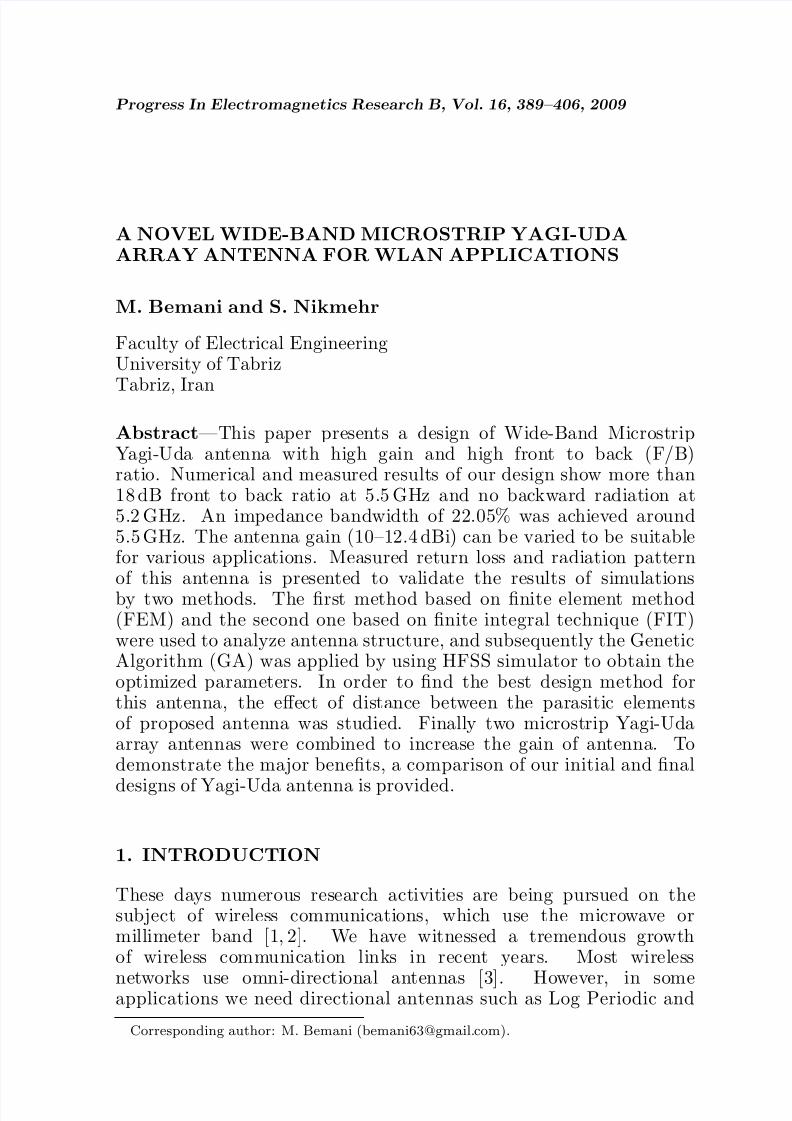
Figure 2. Simulated surface current distributions on the conductors,(a) with slots, (b) without any slots.
8/8/2019 A NOVEL WIDE BAND YAGI-UDA ANTENNA
http://slidepdf.com/reader/full/a-novel-wide-band-yagi-uda-antenna 5/18
Progress In Electromagnetics Research B, Vol. 16, 2009 393
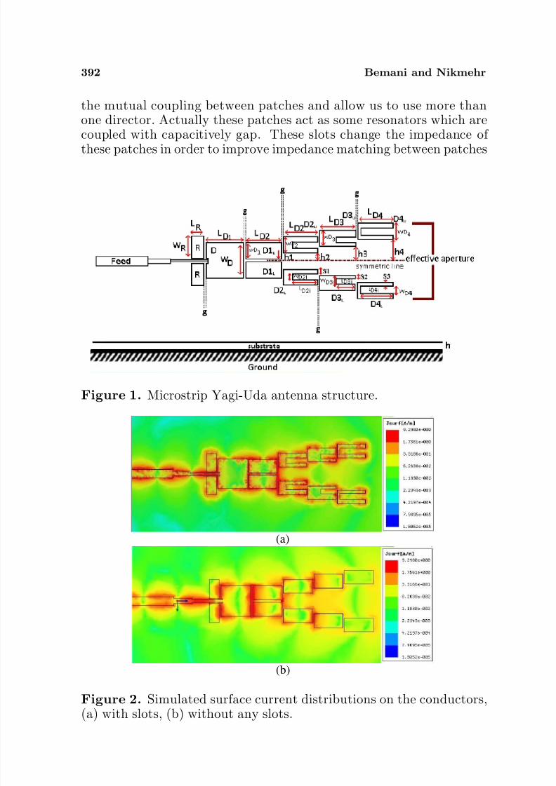
The upper element
(a1)The pattern of upper element
(a2)
The lower element
(b1)The pattern of lower element
(b2)
The combined element
(c1)
The pattern of the combined element
(c2)
0-30
-60
-90
-120
-150
-180
150
90
120
60
30
0
-30
-60
-90
-120
-150
-180
150
90
120
60
30
0
-30
-60
-90
-120
-150-180
150
90
120
60
30
Figure 3. Effect of the upper elements and lower elements.

8/8/2019 A NOVEL WIDE BAND YAGI-UDA ANTENNA
http://slidepdf.com/reader/full/a-novel-wide-band-yagi-uda-antenna 6/18
394 Bemani and Nikmehr
that lead to better transition of energy from feed point to last patch.Fig. 2 shows the effect of these slots. We have also included a slot-
less version of our proposed antenna in this figure to provide a betterinsight of our idea.From Fig. 2, it is obvious that these slots increase the mutual
coupling among the patches, which allows the usage of more patches.However, utilizing 4 additional patches is enough for our application.As can be seen from this figure, the mutual coupling between driven(D) and first director (D1) is already strong enough that there isno need for the application of any slots on the first director (D1).The patches have different lengths and thus have different resonancefrequencies. The driven element has bigger length and, therefore, haslower resonance frequency. Also, from Fig. 2 we realize that withoutslots in director patches, the amount of mutual coupling is not sufficientto excite D2, D3 and D4.
We combine the effect of the upper elements (R, D, D1u , D2u ,D3u, and D4u) and the lower elements (R, D, D1L , D2L , D3L , andD4L) to have a stronger end-fire antenna. Fig. 3 presents the radiationpattern of the upper and lower elements as well as the result of thecombined structure. The upper elements have the peak radiation at60 ≤ ϕ ≤ 75, while the lower elements have the peak radiation
at 105
≤ ϕ ≤ 120
. The pattern of the combined element is muchstronger at ϕ = 90 (note that the purpose of Fig. 3 is presenting theperformance of this antenna, and it will not be utilized in the designprocess).
In order to increase the gain of the antenna, the distance betweenupper and lower directors has to be increased [12]. In fact, the intentionis increasing the effective aperture of Fig. 1, while the amount of coupling between elements is accounted for. In order to have strongcoupling from the driven element D to D1, we have chosen verysmall value for h1. Although, other directors facilitate the presenceof more resonance frequencies, these elements also have the role ingain enhancement of the antenna. As the distance between directorelements increases, the antenna gain would also increase. However, theinadequate distance enlargement would cause an insufficient couplingbetween the pervious and newly added patches, so that the gainimprovement would be suppressed. The relation among these patchesis thoroughly discussed in Section 4.
Note that two reflectors are large enough to decrease the amountof backside radiation. As the simulation results confirm, a larger length
is unnecessary for reducing the backside radiation and just causes theantenna gain reduction.

8/8/2019 A NOVEL WIDE BAND YAGI-UDA ANTENNA
http://slidepdf.com/reader/full/a-novel-wide-band-yagi-uda-antenna 7/18
Progress In Electromagnetics Research B, Vol. 16, 2009 395
Figure 4. Structure of Microstrip Yagi-Uda antenna with angle of ψand equal slots.
Figure 5. Yagi-Uda’s directors that arranged in Thales triangleformat.
3. RESULTS AND DISCUSSION
From Fig. 3, it seems that the performance of this antenna is similarto V -dipole antenna. Therefore, we have arranged our antenna in V-shape. Also, in order to simplify the application of GA we arrangeddirectors and driven patches in the Thales triangle format as can be
seen in Figs. 4 and 5 and considered equal length and width for alldirectors.To achieve the highest gain and front to back ratio, the value of
angle ψ in Fig. 4 has to be optimized. In fact, the best value for ψis equivalent to the best value for h1, h2, h3 and h4. The followingequations can be derived from Fig. 5 to represent the relation betweenψ and hi:
T i = i× g + [(2i− 1)/2]× LD1+ LD (1)
hi = tan(ψ/2)T i −W D1/2 (2)
By optimization of this structure, the best value for ψ is 19.85.To provide a proof of concept to cover a band above and below
5.5 GHz for HIPERLAN applications we have simulated our design
8/8/2019 A NOVEL WIDE BAND YAGI-UDA ANTENNA
http://slidepdf.com/reader/full/a-novel-wide-band-yagi-uda-antenna 8/18
396 Bemani and Nikmehr
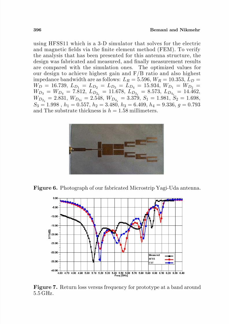
using HFSS11 which is a 3-D simulator that solves for the electricand magnetic fields via the finite element method (FEM). To verify
the analysis that has been presented for this antenna structure, thedesign was fabricated and measured, and finally measurement resultsare compared with the simulation ones. The optimized values forour design to achieve highest gain and F/B ratio and also highestimpedance bandwidth are as follows: LR = 5.596, W R = 10.353, LD =W D = 16.739, LD1
= LD2= LD3
= LD4= 15.934, W D1
= W D2=
W D3= W D4
= 7.812, LD2i= 11.678, LD3i
= 8.573, LD4i= 14.462,
W D2i= 2.831, W D3i
= 2.548, W D4i= 3.379, S 1 = 1.981, S 2 = 1.698,
S 3 = 1.998 , h1 = 0.557, h2 = 3.480, h3 = 6.409, h4 = 9.336, g = 0.793
and The substrate thickness is h = 1.58 millimeters.
Figure 6. Photograph of our fabricated Microstrip Yagi-Uda antenna.
Figure 7. Return loss versus frequency for prototype at a band around5.5 GHz.

8/8/2019 A NOVEL WIDE BAND YAGI-UDA ANTENNA
http://slidepdf.com/reader/full/a-novel-wide-band-yagi-uda-antenna 9/18
Progress In Electromagnetics Research B, Vol. 16, 2009 397
A photograph of this antenna is shown in Fig. 6.In order to measure the return loss of this antenna, an edge-mount
SMA connector was soldered to the edge of the board, and the returnloss was measured on a network analyzer. The simulated and measuredreturn loss versus frequency is presented in Fig. 7.
It can be seen that there are more than two resonance frequenciesin the plot. The first resonance is due to patch D which isbigger than the other patches. The comparative simulation andmeasurement results for our proposed antenna are listed in Table 1.The bandwidth of the prototype antenna due to the measurement,22.05%, is considerably larger than that of the simulated design,14.87%.
It is clear that the performance of microwave systems is severelyaffected by tolerances in the fabrication process. There are threefrequency shifts in the resonances of the measured design whencompared to the simulated results. The third has a frequency shiftof 30 MHz which is small for this design. But the frequency shiftof 110MHz at the 5.2GHz and 5.5GHz resonance can possibly beattributed to a small tolerance in the substrate (RT/Duroid 5880,
Figure 8. Simulated peak antenna gain against frequency for theproposed antenna.
Table 1.
Yagi structure HFSS CST Measurement
Resonant freq 5.19, 5.60, 5.80 5.18, 5.44, 5.82 5.11, 5.42, 5.78
Bandwidth5.04–5.85(14.87%)
5.05–5.90(15.52%)
4.68–5.84(22.05%)
8/8/2019 A NOVEL WIDE BAND YAGI-UDA ANTENNA
http://slidepdf.com/reader/full/a-novel-wide-band-yagi-uda-antenna 10/18
398 Bemani and Nikmehr
εr = 2.2± 0.02).Also the connector was not taken into account in the simulation.
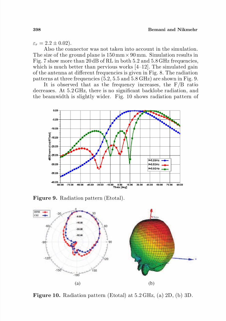
The size of the ground plane is 150 mm× 90 mm. Simulation results inFig. 7 show more than 20 dB of RL in both 5.2 and 5.8 GHz frequencies,which is much better than pervious works [4–12]. The simulated gainof the antenna at different frequencies is given in Fig. 8. The radiationpatterns at three frequencies (5.2, 5.5 and 5.8 GHz) are shown in Fig. 9.
It is observed that as the frequency increases, the F/B ratiodecreases. At 5.2 GHz, there is no significant backlobe radiation, andthe beamwidth is slightly wider. Fig. 10 shows radiation pattern of
Figure 9. Radiation pattern (Etotal).
(a) (b)
0
-30
-60
-90
-120
-150
-180
150
90
120
60
30
Figure 10. Radiation pattern (Etotal) at 5.2 GHz, (a) 2D, (b) 3D.
8/8/2019 A NOVEL WIDE BAND YAGI-UDA ANTENNA
http://slidepdf.com/reader/full/a-novel-wide-band-yagi-uda-antenna 11/18
Progress In Electromagnetics Research B, Vol. 16, 2009 399
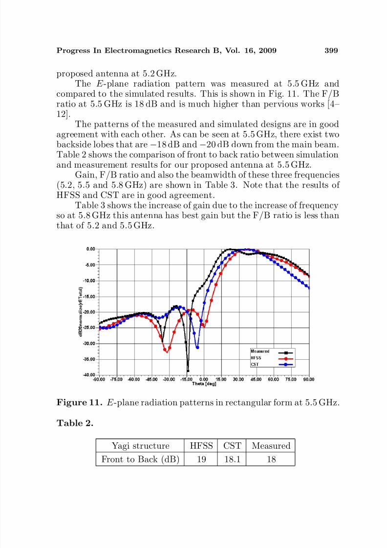
proposed antenna at 5.2 GHz.The E -plane radiation pattern was measured at 5.5 GHz and
compared to the simulated results. This is shown in Fig. 11. The F/Bratio at 5.5 GHz is 18 dB and is much higher than pervious works [4–12].
The patterns of the measured and simulated designs are in goodagreement with each other. As can be seen at 5.5 GHz, there exist twobackside lobes that are −18 dB and−20 dB down from the main beam.Table 2 shows the comparison of front to back ratio between simulationand measurement results for our proposed antenna at 5.5 GHz.
Gain, F/B ratio and also the beamwidth of these three frequencies(5.2, 5.5 and 5.8 GHz) are shown in Table 3. Note that the results of HFSS and CST are in good agreement.
Table 3 shows the increase of gain due to the increase of frequencyso at 5.8 GHz this antenna has best gain but the F/B ratio is less thanthat of 5.2 and 5.5 GHz.
Figure 11. E -plane radiation patterns in rectangular form at 5.5 GHz.
Table 2.
Yagi structure HFSS CST Measured
Front to Back (dB) 19 18.1 18

8/8/2019 A NOVEL WIDE BAND YAGI-UDA ANTENNA
http://slidepdf.com/reader/full/a-novel-wide-band-yagi-uda-antenna 12/18
400 Bemani and Nikmehr
4. PARAMETRIC ANALYSIS
There are many parameters that need to be addressed in this antennastructure. This section gives insight on how these critical parametersaffect the radiation characteristics presented in the tables of thissection. The results of various amounts for h1 are shown on Table 4.Also, instead of studying the effect of h2, h3 and h4 on radiationcharacteristic of antenna we prefer to study just the effect of ψ whichcan cover all variation on h2, h3 and h4. These parameters are variedaround the optimized values given in the previous section. The resultsare at 5.5 GHz and show that we have slight variation for the angleof maximum radiation. It should be considered that other parameters
are constant and equal to value that achieve in last section.
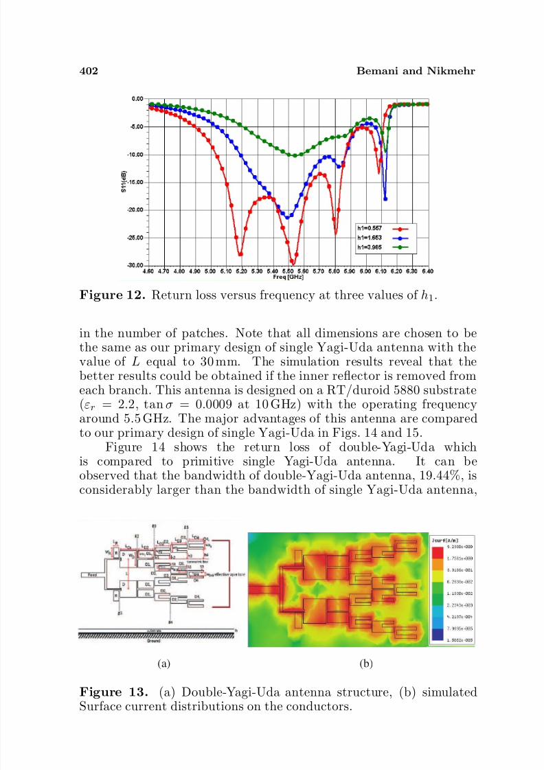
4.1. Variation of h1 at 5.5 GHz
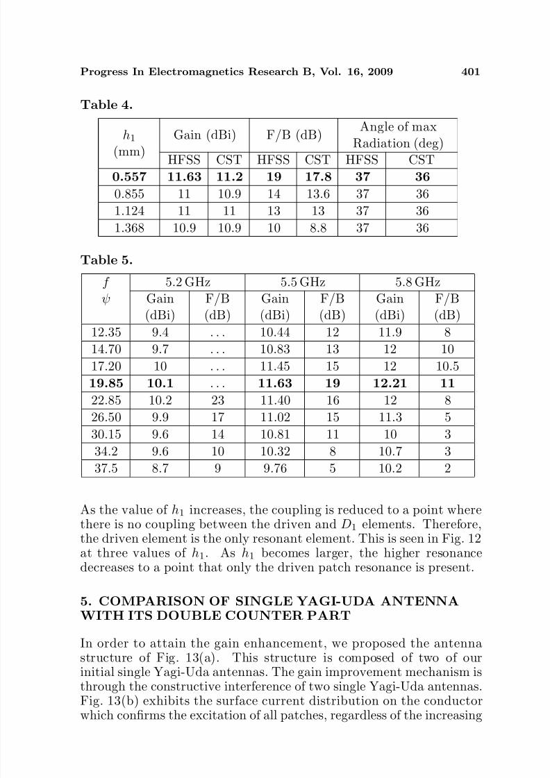
As can be seen in Table 4 the increase of h1 decreases the gain andF/B ratio of the antenna. The major reason for this decline in gainand F/B ratio is the decreased coupling from the driven element tothe D1 element, so we miss an amount of the fields. The best value forthis parameter was found to be 0.557 mm.
4.2. Variation of ψ at 5.5 GHz
The variation of ψ is summarized in Table 5. It can be observed thatthis parameter has a major effect on the gain and F/B ratio because itchanges the effective aperture of the antenna. The best value for thisparameter was found to be ψ = 19.85.
4.3. Bandwidth Variation
It is evident that only D1 has a major effect on bandwidth because D1 isexcited more than other directors, so we just study the variations of h1.
Table 3.
f
(GHz)
Gain (dBi) F/B Ratio (dB)Beamwidth
(degree)
Measured HFSS CST HFSS CST HFSS CST
5.2 10.02 10.1 9.85 . . . . . . 54 525.5 11.93 11.63 11.48 19 18.1 37 36
5.8 12.01 12.21 11.90 11 10 32 30
8/8/2019 A NOVEL WIDE BAND YAGI-UDA ANTENNA
http://slidepdf.com/reader/full/a-novel-wide-band-yagi-uda-antenna 13/18
Progress In Electromagnetics Research B, Vol. 16, 2009 401
Table 4.
h1
(mm)Gain (dBi) F/B (dB)
Angle of max
Radiation (deg)
HFSS CST HFSS CST HFSS CST
0.557 11.63 11.2 19 17.8 37 36
0.855 11 10.9 14 13.6 37 36
1.124 11 11 13 13 37 36
1.368 10.9 10.9 10 8.8 37 36
Table 5.
f
ψ
5.2 GHz 5.5 GHz 5.8 GHz
Gain(dBi)
F/B(dB)
Gain(dBi)
F/B(dB)
Gain(dBi)
F/B(dB)
12.35 9.4 . . . 10.44 12 11.9 8
14.70 9.7 . . . 10.83 13 12 10
17.20 10 . . . 11.45 15 12 10.5
19.85 10.1 . . . 11.63 19 12.21 11
22.85 10.2 23 11.40 16 12 8
26.50 9.9 17 11.02 15 11.3 5
30.15 9.6 14 10.81 11 10 3
34.2 9.6 10 10.32 8 10.7 3
37.5 8.7 9 9.76 5 10.2 2
As the value of h1 increases, the coupling is reduced to a point wherethere is no coupling between the driven and D1 elements. Therefore,
the driven element is the only resonant element. This is seen in Fig. 12at three values of h1. As h1 becomes larger, the higher resonancedecreases to a point that only the driven patch resonance is present.
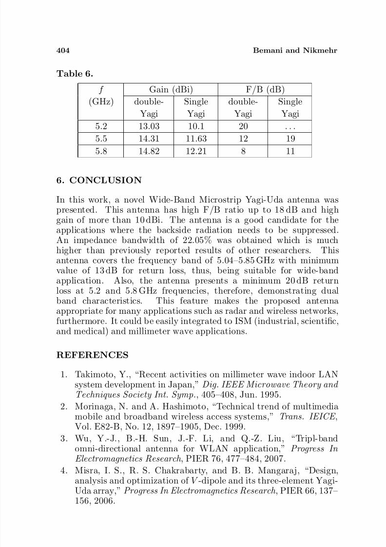
5. COMPARISON OF SINGLE YAGI-UDA ANTENNAWITH ITS DOUBLE COUNTER PART
In order to attain the gain enhancement, we proposed the antennastructure of Fig. 13(a). This structure is composed of two of ourinitial single Yagi-Uda antennas. The gain improvement mechanism isthrough the constructive interference of two single Yagi-Uda antennas.Fig. 13(b) exhibits the surface current distribution on the conductorwhich confirms the excitation of all patches, regardless of the increasing
8/8/2019 A NOVEL WIDE BAND YAGI-UDA ANTENNA
http://slidepdf.com/reader/full/a-novel-wide-band-yagi-uda-antenna 14/18
402 Bemani and Nikmehr
Figure 12. Return loss versus frequency at three values of h1.
in the number of patches. Note that all dimensions are chosen to bethe same as our primary design of single Yagi-Uda antenna with thevalue of L equal to 30 mm. The simulation results reveal that thebetter results could be obtained if the inner reflector is removed fromeach branch. This antenna is designed on a RT/duroid 5880 substrate
(εr = 2.2, tanσ = 0.0009 at 10 GHz) with the operating frequencyaround 5.5 GHz. The major advantages of this antenna are comparedto our primary design of single Yagi-Uda in Figs. 14 and 15.
Figure 14 shows the return loss of double-Yagi-Uda whichis compared to primitive single Yagi-Uda antenna. It can beobserved that the bandwidth of double-Yagi-Uda antenna, 19.44%, isconsiderably larger than the bandwidth of single Yagi-Uda antenna,
(a) (b)
Figure 13. (a) Double-Yagi-Uda antenna structure, (b) simulatedSurface current distributions on the conductors.

8/8/2019 A NOVEL WIDE BAND YAGI-UDA ANTENNA
http://slidepdf.com/reader/full/a-novel-wide-band-yagi-uda-antenna 15/18
Progress In Electromagnetics Research B, Vol. 16, 2009 403
Figure 14. Simulated return loss of double and single Yagi-Udaantenna.
Figure 15. 2-D radiation pattern of the double-Yagi and single-Yagiarray at 5.5 GHz.
14.87%.The radiation pattern of this antenna at 5.5 GHz is illustrated as
well as its comparison with the radiation pattern of our initial antennain Fig. 15.
The angle of maximum radiation for both antennas is between
30
–40
, while the beamwidth is approximately 35
. The gain andfront to back ratio for both antennas are presented at three frequencies(5.2, 5.5, 5.8 GHz) in Table 6.
8/8/2019 A NOVEL WIDE BAND YAGI-UDA ANTENNA
http://slidepdf.com/reader/full/a-novel-wide-band-yagi-uda-antenna 16/18
404 Bemani and Nikmehr
Table 6.
f
(GHz)
Gain (dBi) F/B (dB)
double-
Yagi
Single
Yagi
double-
Yagi
Single
Yagi
5.2 13.03 10.1 20 . . .
5.5 14.31 11.63 12 19
5.8 14.82 12.21 8 11
6. CONCLUSION
In this work, a novel Wide-Band Microstrip Yagi-Uda antenna waspresented. This antenna has high F/B ratio up to 18 dB and highgain of more than 10 dBi. The antenna is a good candidate for theapplications where the backside radiation needs to be suppressed.An impedance bandwidth of 22.05% was obtained which is muchhigher than previously reported results of other researchers. Thisantenna covers the frequency band of 5.04–5.85 GHz with minimumvalue of 13 dB for return loss, thus, being suitable for wide-bandapplication. Also, the antenna presents a minimum 20 dB returnloss at 5.2 and 5.8 GHz frequencies, therefore, demonstrating dualband characteristics. This feature makes the proposed antennaappropriate for many applications such as radar and wireless networks,furthermore. It could be easily integrated to ISM (industrial, scientific,and medical) and millimeter wave applications.
REFERENCES
1. Takimoto, Y., “Recent activities on millimeter wave indoor LAN
system development in Japan,” Dig. IEEE Microwave Theory and Techniques Society Int. Symp., 405–408, Jun. 1995.
2. Morinaga, N. and A. Hashimoto, “Technical trend of multimediamobile and broadband wireless access systems,” Trans. IEICE ,Vol. E82-B, No. 12, 1897–1905, Dec. 1999.
3. Wu, Y.-J., B.-H. Sun, J.-F. Li, and Q.-Z. Liu, “Tripl-bandomni-directional antenna for WLAN application,” Progress In Electromagnetics Research , PIER 76, 477–484, 2007.
4. Misra, I. S., R. S. Chakrabarty, and B. B. Mangaraj, “Design,
analysis and optimization of V -dipole and its three-element Yagi-Uda array,” Progress In Electromagnetics Research , PIER 66, 137–156, 2006.
8/8/2019 A NOVEL WIDE BAND YAGI-UDA ANTENNA
http://slidepdf.com/reader/full/a-novel-wide-band-yagi-uda-antenna 17/18
Progress In Electromagnetics Research B, Vol. 16, 2009 405
5. Tran, A. and M. C. E. Yagoub, “Intertwined two-section dual-polarized log periodic dipole antenna,” PIERS Proceedings, 30–33,
Prague, Czech Republic, Aug. 27–30, 2007.6. Densmore, A. and J. Huang, “Microstrip Yagi antenna for mobile
satellite service,” IEEE Antennas and Propagation Society Int.Symp., Vol. 2, 616–619, Jun. 1991.
7. Zhang, X. C., J. G. Liang, and J. W. Xie, “The Quasi-Yagiantenna subarrat fed by an orthogonal T junction,” Progress In Electromagnetics Research Letters, Vol. 4, 109–112, 2008.
8. Chen, C. A. and D. K Cheng, “Optimum element lengths for Yagi-Uda arrays,” IEEE Trans. Antennas and Propagation , Vol. 23,
Jan. 1975.9. Lee, K. F., et al., “Microstrip antenna array with parasitic
elements,” IEEE Antennas and Propagation Society Symposium Dig., 794–797, Jun. 1987.
10. Haneishi, M., et al., “Beam-shaping of microstrip antenna byparasitic elements having coaxial stub,” Trans. IECE of Japan ,Vol. 69-B, 1160–1161, 1986.
11. Huang, J., “Planar microstrip Yagi array antenna,” IEEE Antennas and Propagation Society Int. Symp., Vol. 2, 894–897,
Jun. 1989.12. Gray, D., J. Lu, and D. Thiel, “Electronically steerable Yagi-
Uda microstrip patch antenna array,” IEEE Trans. Antennas and Propagation , Vol. 46, No. 5, 605–608, May 1998.
13. Padhi, S. and M. Bialkowski, “Investigations of an aperturecoupled microstrip Yagi antenna using PBG structure,” IEEE Antennas and Propagation Society Int. Symp., Vol. 3, 752–755,Jun. 2002.
14. Yablonovitch, E., “Photonic band-gap structures,” Journal of
Optical Society of America B , Vol. 10, 283–295, 1993.15. Yang, F., K. Mu, Y. Quin, and T. Itoh, “A unipolar photonic
bandgap (UC-PBG) structure and its applications for microwavecircuits,” IEEE Trans. Microwave Theory Technique, Vol. 47,1509–1514, Aug. 1999.
16. Fu, Y. Q., G. H. Zhang, and N. C. Yuan, “A novel PBG coplanarwaveguide,” IEEE Microwave and Wireless Components Letters,Vol. 11, Nov. 2001,
17. Gonzalo, R., P. D. Maagt, and M. Sorolla, “Enhanced patch-
antenna performance by suppressing surface waves by usingphotonic bandgap substrates,” IEEE Trans. Microwave Theory and Techniques, Vol. 47, 2131–2139, Nov. 1999.
8/8/2019 A NOVEL WIDE BAND YAGI-UDA ANTENNA
http://slidepdf.com/reader/full/a-novel-wide-band-yagi-uda-antenna 18/18
406 Bemani and Nikmehr
18. DeJean, G. R. and M. M. Tentzeris , “A new high-gain microstripYagi array antenna with a high front-to-back (F/B) ratio for
WLAN and millimeter-wave applications,” IEEE Trans. Antennasand Propagation , Vol. 55, Feb. 2007.
19. HFSS: High frequency structure simulator based on thefiniteElement method, v. 9.2.1, Ansoft Corporation, 2004.
20. CST GmbH 2008 CST MICROWAVE STUDIO(r) User ManualV. 5.0, Darmstadt, Germany (www.cst.de).
21. R/T Duroid Laminates, Rogers Corporation, Rogers, CT, 2008.


![Currents on Generalized Yagi StructuresAs recounted by Professor Uda 11,2], the Yagi-Uda antenna was invented in 1926. Further practical and theoretical studies were undertaken, but,](https://img.pdfslide.net/doc/110x75/5e94290536a67159ca4acd82/currents-on-generalized-yagi-structures-as-recounted-by-professor-uda-112-the.jpg)