Embed Size (px)
Citation preview
AB31 Zener Voltage Regulator
Operating Manual Ver.1.1
An ISO 9001 : 2000 company
94-101, Electronic Complex Pardesipura, Indore- 452010, India Tel : 91-731- 2570301/02, 4211100 Fax: 91- 731- 2555643 e mail : [email protected] Website : www.scientech.bz Toll free : 1800-103-5050

AB31
Scientech Technologies Pvt. Ltd. 2
AB31
Scientech Technologies Pvt. Ltd. 3
RoHS Compliance
Scientech Products are RoHS Complied. RoHS Directive concerns with the restrictive use of Hazardous substances (Pb, Cd, Cr, Hg, Br compounds) in electric and electronic equipments. Scientech products are “Lead Free” and “Environment Friendly”. It is mandatory that service engineers use lead free solder wire and use the soldering irons upto (25 W) that reach a temperature of 450°C at the tip as the melting temperature of the unleaded solder is higher than the leaded solder.
AB31 Zener Voltage Regulator
Table of Contents
1. Introduction 4
2. Theory 6 3. Experiments
• Experiment 1 8 Study of Zener diode as a voltage regulator, when input voltage Vin is fixed while Load resistance RL is variable.
• Experiment 2 11 Study of Zener diode as a voltage regulator, when input voltage Vin is variable while Load resistance RL is fixed.
4. Data Sheet 14
5. Warranty 15 6. List of Accessories 15
AB31
Scientech Technologies Pvt. Ltd. 4
Introduction AB31 is a compact, ready to use Zener Voltage Regulator experiment board. This is useful for students to study the operation of zener diode as a voltage regulator with the variation in source voltage and load resistance. It can be used as stand alone unit with external DC Power Supply or can be used with Scientech Analog Lab ST2612 which has built in DC Power Supply, AC Power Supply, function generator, modulation generator, continuity tester, toggle switches, and potentiometer.
List of Boards : Model Name AB01 Diode characteristics (Si, Zener, LED) AB02 Transistor characteristics (CB NPN) AB03 Transistor characteristics (CB PNP) AB04 Transistor characteristics (CE NPN) AB05 Transistor characteristics (CE PNP) AB06 Transistor characteristics (CC NPN) AB07 Transistor characteristics (CC PNP) AB08 FET characteristics AB09 Rectifier Circuits AB10 Wheatstone bridge AB11 Maxwell’s Bridge AB12 De Sauty’s Bridge AB13 Schering Bridge AB14 Darlington Pair AB15 Common Emitter Amplifier AB16 Common Collector Amplifier AB17 Common Base Amplifier AB18 RC-Coupled Amplifier AB19 Cascode Amplifier AB20 Direct Coupled Amplifier AB21 Class A Amplifier AB22 Class B Amplifier (push pull emitter follower) AB23 Class C Tuned Amplifier AB24 Transformer Coupled Amplifier AB25 Phase Locked Loop (FM Demodulator & Frequency Divider / Multiplier) AB26 FET Amplifier AB27 Voltage Controlled Oscillator AB28 Multivibrator (Mono stable/Astable) AB29 F-V and V-F Converter AB30 V-I and I-V Converter AB32 Transistor Series Voltage Regulator AB33 Transistor Shunt Voltage Regulator AB35 DC Ammeter AB37 DC Ammeter (0-2mA)
AB31
Scientech Technologies Pvt. Ltd. 5
AB39 Instrumentation Amplifier AB41 Differential Amplifier (Transistorized) AB42 Operational Amplifier (Inverting / Non-inverting / Differentiator) AB43 Operational Amplifier (Adder/Scalar) AB44 Operational Amplifier (Integrator/ Differentiator) AB45 Schmitt Trigger and Comparator AB49 K Derived Filter AB51 Active filters (Low Pass and High Pass) AB52 Active Band Pass Filter AB54 Tschebyscheff Filter AB56 Fiber Optic Analog Link AB57 Owen’s Bridge AB58 Anderson’s Bridge AB59 Maxwell’s Inductance Bridge AB64 RC – Coupled Amplifier with Feedback AB66 Wien Bridge Oscillators AB67 Colpitt Oscillator AB68 Hartley Oscillator AB80 RLC Series and RLC Parallel Resonance AB82 Thevenin’s and Maximum Power Transfer Theorem AB83 Reciprocity and Superposition Theorem AB84 Tellegen’s Theorem AB85 Norton’s theorem AB88 Diode Clipper AB89 Diode Clampers AB90 Two port network parameter AB91 Optical Transducer (Photovoltaic cell) AB92 Optical Transducer (Photoconductive cell/LDR) AB93 Optical Transducer (Phototransistor) AB96 Temperature Transducer (RTD & IC335) AB97 Temperature Transducer (Thermocouple) AB101 DSB Modulator and Demodulator AB102 SSB Modulator and Demodulator AB106 FM Modulator and Demodulator
and many more…………
AB31
Scientech Technologies Pvt. Ltd. 6
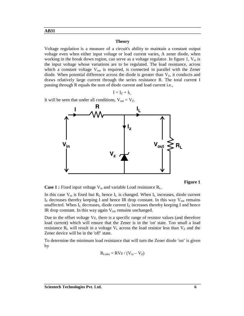
Theory Voltage regulation is a measure of a circuit's ability to maintain a constant output voltage even when either input voltage or load current varies, A zener diode, when working in the break down region, can serve as a voltage regulator. In figure 1, Vin is the input voltage whose variations are to be regulated. The load resistance, across which a constant voltage Vout is required, is connected in parallel with the Zener diode. When potential difference across the diode is greater than VZ, it conducts and draws relatively large current through the series resistance R. The total current I passing through R equals the sum of diode current and load current i.e.,
I = IZ + IL.
It will be seen that under all conditions, Vout = VZ.
Figure 1 Case 1 : Fixed input voltage Vin and variable Load resistance RL. In this case Vin is fixed but RL hence IL is changed. When IL increases, diode current IZ decreases thereby keeping I and hence IR drop constant. In this way Vout remains unaffected. When IL decreases, diode current IZ increases thereby keeping I and hence IR drop constant. In this way again Vout remains unchanged. Due to the offset voltage Vz, there is a specific range of resistor values (and therefore load current) which will ensure that the Zener is in the 'on' state. Too small a load resistance RL will result in a voltage VL across the load resistor less than VZ and the Zener device will be in the 'off’ state.
To determine the minimum load resistance that will turn the Zener diode ‘on’ is given by
RLmin = RVz / (Vin – VZ)

AB31
Scientech Technologies Pvt. Ltd. 7
Any load resistance value greater than the RL obtained from above equation will ensure that the zener diode is in the ‘on’ state and the diode can be replaced by its VZ source equivalent. Similarly maximum load resistance is given by
RLmax = VZ / ILmin Where
ILmin = IR - IZM IR = VR / R,
VR = Vin - VZ Case 2 : Variable input voltage Vi and fixed load resistance RL.
In this case, when input voltage Vin is increased slightly keeping load resistance RL constant. It will increase I. This increase in I will be absorbed by the Zener diode without affecting IL. This increase in Vin will be dropped across R thereby keeping Vout constant.
Conversely, if supply voltage Vin falls, the diode takes a smaller current and voltage drop across R is reduced, thus again keeping Vout constant.
Hence, when Vin changes, I and IR drop change in such a way as to keep Vout (= VZ) constant.
For fixed value of RL, the voltage Vin must be sufficiently large to turn the Zener diode ‘‘on’’. The minimum turn-on voltage Vi(min) is determined by
Vi(min) = (RL + R)VZ / RL The maximum value of Vi is limited by the maximum Zener current IZM. Since
IZM = IR - IL, IRmax = IZM + IL Since IL if fixed at VZ/RL and IZM is the maximum value of Iz, the maximum Vin is defined by
Vi(max) = IRmax R + V z
Note : 1. Regulated output voltage might be slightly higher than the expected voltage due
to tolerance of Zener diode. 2. A series resistor of 33 ohms is connected internally with potentiometer P1, for
over current protection thus the maximum voltage that you can get at test point I is about 9.5V
AB31
Scientech Technologies Pvt. Ltd. 8
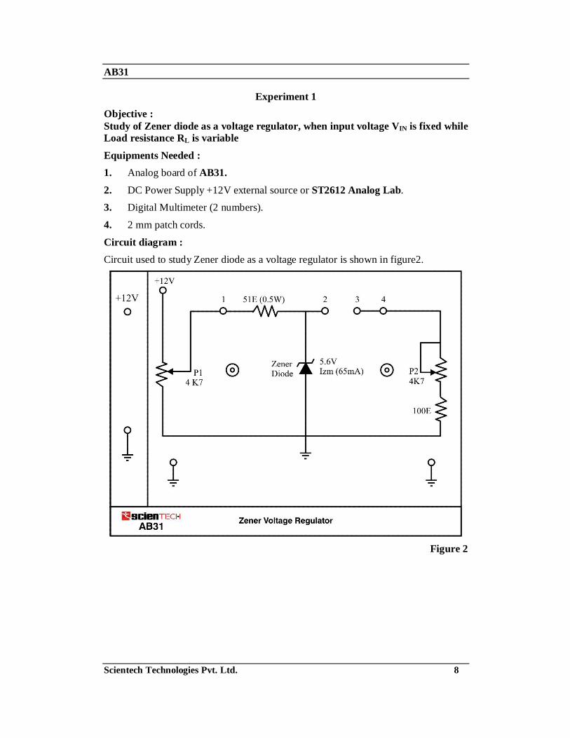
Experiment 1 Objective : Study of Zener diode as a voltage regulator, when input voltage VIN is fixed while Load resistance RL is variable Equipments Needed : 1. Analog board of AB31. 2. DC Power Supply +12V external source or ST2612 Analog Lab. 3. Digital Multimeter (2 numbers).
4. 2 mm patch cords.
Circuit diagram : Circuit used to study Zener diode as a voltage regulator is shown in figure2.
Figure 2
AB31
Scientech Technologies Pvt. Ltd. 9
Procedure : 1. Connect + 12V DC Power Supply at their indicated position from external
source or ST2612 Analog Lab. 2. Connect one voltmeter between test point 1 and ground to measure input voltage
Vin.
3. Connect ohmmeter between test point 4 and ground and set the value of load resistance RL at some fixed value (500Ω, 600Ω, ……..1K, 1.1K )
4. Connect a 2mm patch cord between test point 2 and 3.
5. Connect voltmeter between test point 4 and ground to measure output voltage Vout.
6. Switch on the Power Supply.
7. Vary the potentiometer P1 to set fixed value of input voltage Vin=10V and measure the corresponding value of output voltage Vout.
8. Disconnect the 2mm patch cord between test point 2 and 3. 9. Repeat the procedure from step 3 for different sets of load resistance RL and
note the results in an observation Table 1.
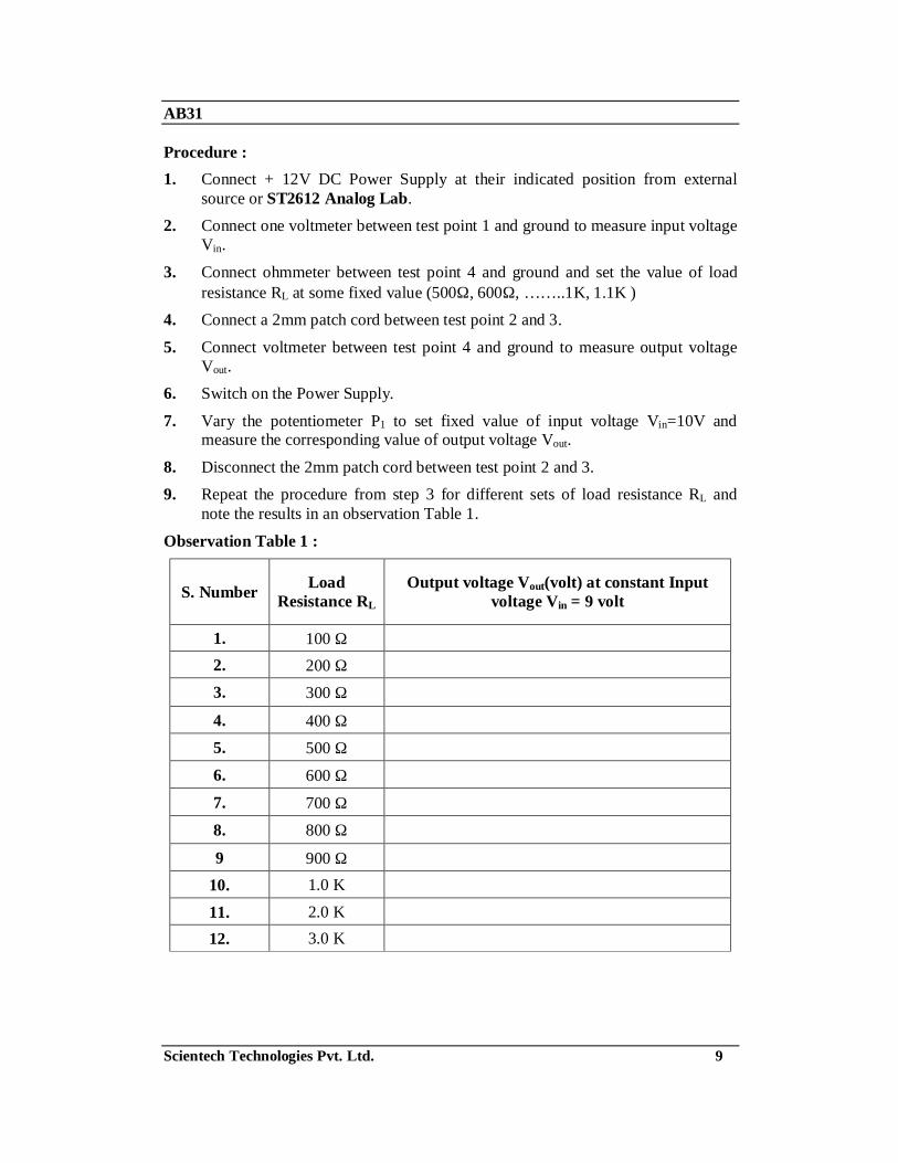
Observation Table 1 :
S. Number Load Resistance RL
Output voltage Vout(volt) at constant Input voltage Vin = 9 volt
1. 100 Ω 2. 200 Ω
3. 300 Ω
4. 400 Ω
5. 500 Ω
6. 600 Ω
7. 700 Ω
8. 800 Ω
9 900 Ω
10. 1.0 K
11. 2.0 K 12. 3.0 K
AB31
Scientech Technologies Pvt. Ltd. 10
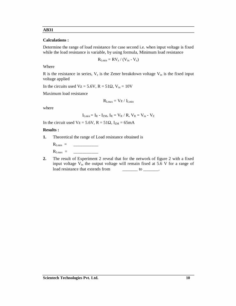
Calculations : Determine the range of load resistance for case second i.e. when input voltage is fixed while the load resistance is variable, by using formula, Minimum load resistance
RLmin = RVz / (Vin - Vz)
Where R is the resistance in series, Vz is the Zener breakdown voltage Vin is the fixed input voltage applied
In the circuits used Vz = 5.6V, R = 51Ω, Vin = 10V
Maximum load resistance
RLmax = Vz / ILmin where
ILmin = IR - IZM, IR = VR / R, VR = Vin - VZ
In the circuit used Vz = 5.6V, R = 51Ω, IZM = 65mA
Results : 1. Theoretical the range of Load resistance obtained is
RLmin = ___________ RLmax = ___________
2. The result of Experiment 2 reveal that for the network of figure 2 with a fixed input voltage Vin the output voltage will remain fixed at 5.6 V for a range of load resistance that extends from _______ to _______.
AB31
Scientech Technologies Pvt. Ltd. 11
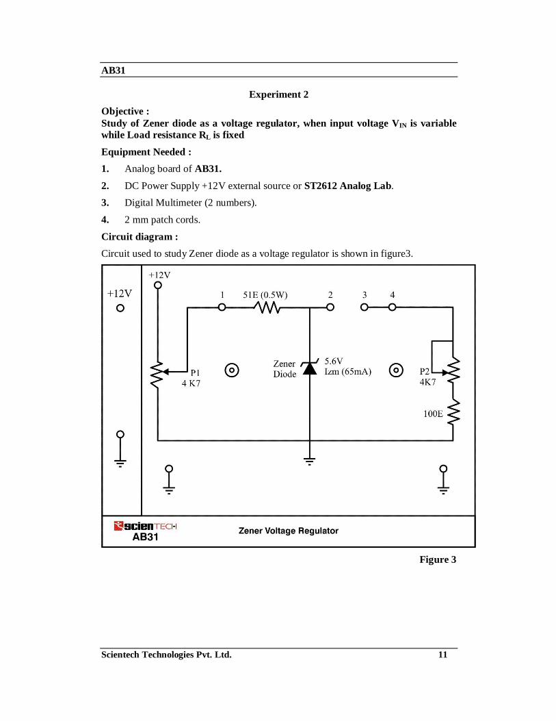
Experiment 2 Objective : Study of Zener diode as a voltage regulator, when input voltage VIN is variable while Load resistance RL is fixed Equipment Needed : 1. Analog board of AB31. 2. DC Power Supply +12V external source or ST2612 Analog Lab. 3. Digital Multimeter (2 numbers).
4. 2 mm patch cords.
Circuit diagram : Circuit used to study Zener diode as a voltage regulator is shown in figure3.
Figure 3
AB31
Scientech Technologies Pvt. Ltd. 12
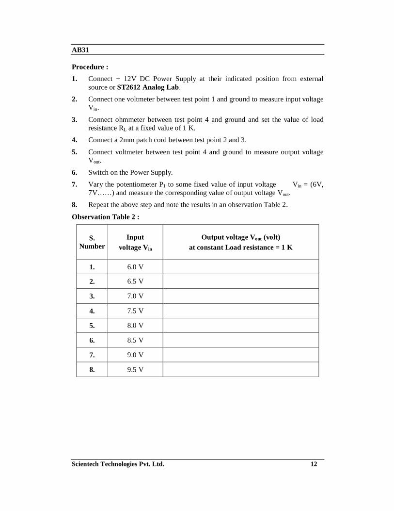
Procedure : 1. Connect + 12V DC Power Supply at their indicated position from external
source or ST2612 Analog Lab. 2. Connect one voltmeter between test point 1 and ground to measure input voltage
Vin.
3. Connect ohmmeter between test point 4 and ground and set the value of load resistance RL at a fixed value of 1 K.
4. Connect a 2mm patch cord between test point 2 and 3.
5. Connect voltmeter between test point 4 and ground to measure output voltage Vout.
6. Switch on the Power Supply. 7. Vary the potentiometer P1 to some fixed value of input voltage Vin = (6V,
7V……) and measure the corresponding value of output voltage Vout. 8. Repeat the above step and note the results in an observation Table 2.
Observation Table 2 :
S. Number
Input voltage Vin
Output voltage Vout (volt) at constant Load resistance = 1 K
1. 6.0 V
2. 6.5 V
3. 7.0 V
4. 7.5 V
5. 8.0 V
6. 8.5 V
7. 9.0 V
8. 9.5 V
AB31
Scientech Technologies Pvt. Ltd. 13
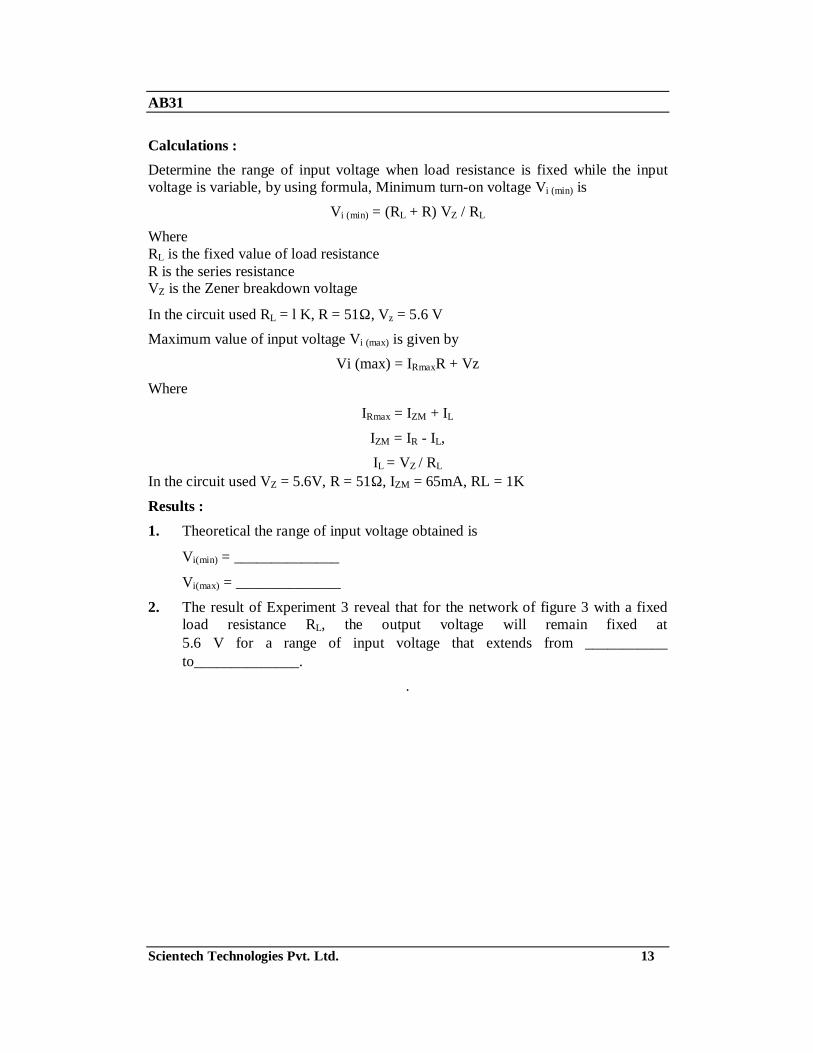
Calculations : Determine the range of input voltage when load resistance is fixed while the input voltage is variable, by using formula, Minimum turn-on voltage Vi (min) is
Vi (min) = (RL + R) VZ / RL
Where RL is the fixed value of load resistance R is the series resistance VZ is the Zener breakdown voltage
In the circuit used RL = l K, R = 51Ω, Vz = 5.6 V Maximum value of input voltage Vi (max) is given by
Vi (max) = IRmaxR + Vz
Where IRmax = IZM + IL
IZM = IR - IL, IL = VZ / RL
In the circuit used VZ = 5.6V, R = 51Ω, IZM = 65mA, RL = 1K
Results : 1. Theoretical the range of input voltage obtained is
Vi(min) = ______________
Vi(max) = ______________
2. The result of Experiment 3 reveal that for the network of figure 3 with a fixed load resistance RL, the output voltage will remain fixed at 5.6 V for a range of input voltage that extends from ___________ to______________.
.
AB31
Scientech Technologies Pvt. Ltd. 14
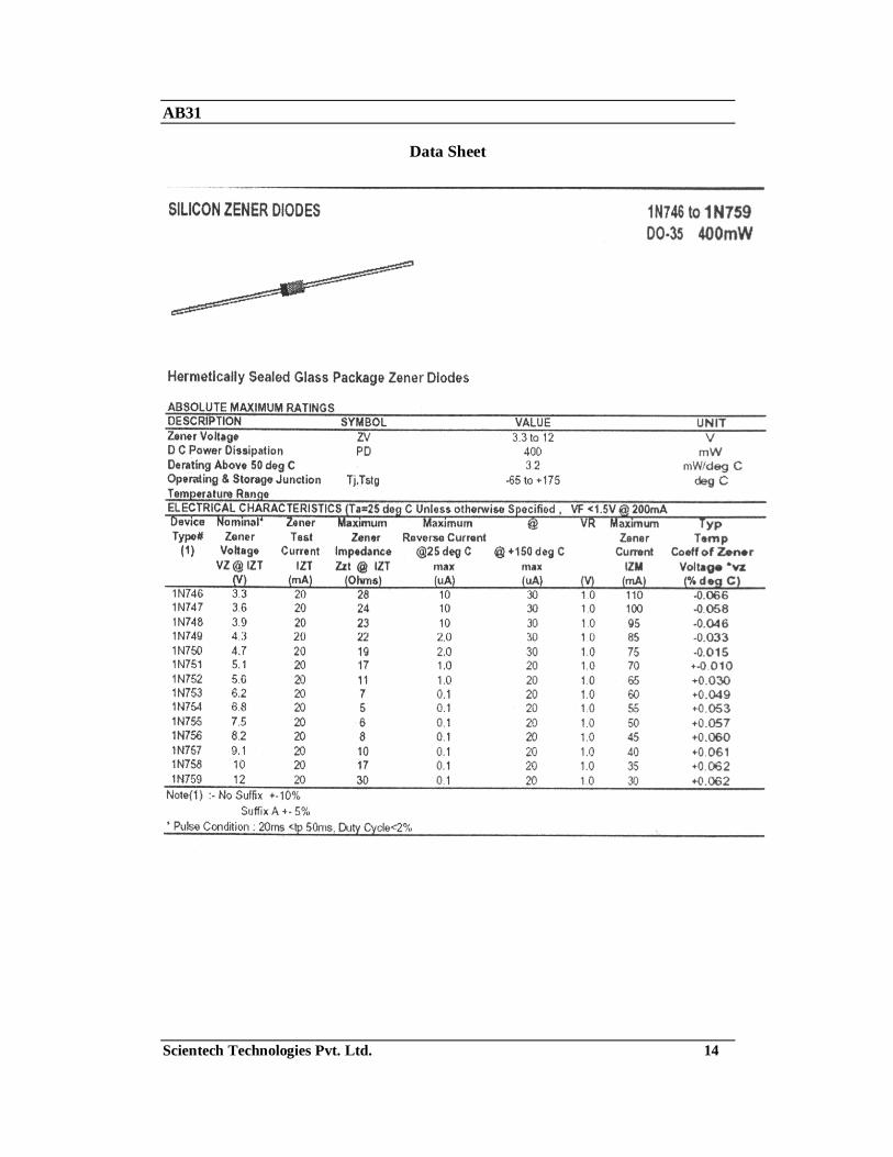
Data Sheet
AB31
Scientech Technologies Pvt. Ltd. 15
Warranty 1. We guarantee the product against all manufacturing defects for 24 months from
the date of sale by us or through our dealers. Consumables like dry cell etc. are not covered under warranty.
2. The guarantee will become void, if
a) The product is not operated as per the instruction given in the operating manual.
b) The agreed payment terms and other conditions of sale are not followed.
c) The customer resells the instrument to another party. d) Any attempt is made to service and modify the instrument.
3. The non-working of the product is to be communicated to us immediately giving full details of the complaints and defects noticed specifically mentioning the type, serial number of the product and date of purchase etc.
4. The repair work will be carried out, provided the product is dispatched securely packed and insured. The transportation charges shall be borne by the customer.
For any Technical Problem Please Contact us at [email protected]
List of Accessories
1. 2 mm Patch Cords (Red) ...................................................................... 2 Nos. 2. 2 mm Patch Cord (Blue) ....................................................................... 4 Nos. 3. 2 mm Patch Cord (Black) ..................................................................... 4 Nos. 4. e-Manual.................................................................................................1 No.
Updated 25-03-2009