Embed Size (px)
Citation preview

ADP1055-EVALZ User GuideUG-710
One Technology Way • P.O. Box 9106 • Norwood, MA 02062-9106, U.S.A. • Tel: 781.329.4700 • Fax: 781.461.3113 • www.analog.com
Evaluating the 240 Watts ADP1055 Digital Controller for
Isolated Power Supply with PMBus Interface
PLEASE SEE THE LAST PAGE FOR AN IMPORTANT WARNING AND LEGAL TERMS AND CONDITIONS. Rev. B | Page 1 of 43
FEATURES Full support evaluation kit for the ADP1055 240 W full bridge topology (adjustable to phase shifted full
bridge topology) Rated power of 12 V dc, 20 A PMBus Revision 1.2 compliant with PEC and extended
manufacturer specific commands 32-bit password protection with command masking 64 address selections (16 base addresses, expandable to 64) 6 PWM control signals, 625 ps resolution Duty cycle double update rate Fast line voltage feedforward Redundant programmable OVP Frequency synchronization Soft-start and soft-stop functionality Droop current sharing On-board tests for housekeeping functions PMBus communication Software GUI
EVALUATION KIT CONTENTS ADP1055-EVALZ evaluation board ADP1055DC1-EVALZ daughter card
ADDITIONAL EQUIPMENT NEEDED The USB-I2C connector, ADP-I2C-USB-Z, with Driver CD
(must order separately from Analog Devices, Inc.)
GENERAL DESCRIPTION This evaluation board, together with a daughter card, allows you to evaluate the ADP1055 as a power supply application. With the USB to I2C connector, and the graphical user interface (GUI), the ADP1055 on the evaluation board can be interfaced with a PC via a USB port.
The evaluation board is set up to act as an isolated PSU with a rated load of 12 V, 20 A from a 38 V dc to 60 V dc source.
Connectors on the evaluation board provide synchronization, as well as share bus and PMBus™ interfaces, allowing direct parallel evaluation when multiple evaluation boards are connected in parallel to a common bus.
Multiple test points allow easy access to all critical points/pins.
EVALUATION BOARD SETUP 12
386-
001
Figure 1. ADP1055 Evaluation Board
UG-710 ADP1055-EVALZ User Guide
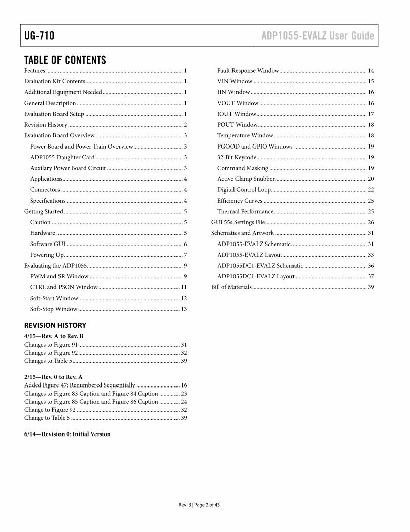
TABLE OF CONTENTS Features .............................................................................................. 1 Evaluation Kit Contents ................................................................... 1 Additional Equipment Needed ....................................................... 1 General Description ......................................................................... 1 Evaluation Board Setup ................................................................... 1 Revision History ............................................................................... 2 Evaluation Board Overview ............................................................ 3
Power Board and Power Train Overview .................................. 3 ADP1055 Daughter Card ............................................................ 3 Auxilary Power Board Circuit .................................................... 3 Applications ................................................................................... 4 Connectors .................................................................................... 4 Specifications ................................................................................ 4
Getting Started .................................................................................. 5 Caution .......................................................................................... 5 Hardware ....................................................................................... 5 Software GUI ................................................................................ 6 Powering Up .................................................................................. 7
Evaluating the ADP1055.................................................................. 9 PWM and SR Window ................................................................ 9 CTRL and PSON Window ........................................................ 11 Soft-Start Window ...................................................................... 12 Soft-Stop Window ...................................................................... 13
Fault Response Window ............................................................ 14 VIN Window .............................................................................. 15 IIN Window ................................................................................ 16 VOUT Window .......................................................................... 16 IOUT Window ............................................................................ 17 POUT Window ........................................................................... 18 Temperature Window ................................................................ 18 PGOOD and GPIO Windows .................................................. 19 32-Bit Keycode ............................................................................ 19 Command Masking ................................................................... 19 Active Clamp Snubber ............................................................... 20 Digital Control Loop.................................................................. 22 Efficiency Curves ....................................................................... 25 Thermal Performance ................................................................ 25
GUI 55s Settings File ...................................................................... 26 Schematics and Artwork ............................................................... 31
ADP1055-EVALZ Schematic .................................................... 31 ADP1055-EVALZ Layout .......................................................... 33 ADP1055DC1-EVALZ Schematic ........................................... 36 ADP1055DC1-EVALZ Layout ................................................. 37
Bill of Materials ............................................................................... 39
REVISION HISTORY 4/15—Rev. A to Rev. B Changes to Figure 91 ...................................................................... 31 Changes to Figure 92 ...................................................................... 32 Changes to Table 5 .......................................................................... 39 2/15—Rev. 0 to Rev. A Added Figure 47; Renumbered Sequentially .............................. 16 Changes to Figure 83 Caption and Figure 84 Caption .............. 23 Changes to Figure 85 Caption and Figure 86 Caption .............. 24 Change to Figure 92 ....................................................................... 32 Change to Table 5 ........................................................................... 39 6/14—Revision 0: Initial Version
Rev. B | Page 2 of 43

ADP1055-EVALZ User Guide UG-710
Rev. B | Page 3 of 43
EVALUATION BOARD OVERVIEW This ADP1055-EVALZ evaluation board and ADP1055DC1-EVALZ daughter card feature the ADP1055 in a dc-to-dc switching power supply in full bridge topology with synchronous rectification operating at 125 kHz switching frequency.
Figure 4 shows the block diagram of the evaluation board. The circuit is designed to provide a rated load of 12 V, 20 A from a dc input voltage source of 38 V dc to 60 V dc. The ADP1055 provides functions, including output voltage regulation, synchronization, constant current control, pre-bias start up, and comprehensive protection functions.
The evaluation kit consists of a power board, daughter card, and the auxiliary circuit board.
POWER BOARD AND POWER TRAIN OVERVIEW The power board is shown in Figure 1. Referring to the Schematics and Artwork section, the circuit components are described as follows. The primary and secondary H bridges are formed with MOSFETs QA through QD (primary side) and MOSFETs Q30, Q34, Q38, and Q40 (secondary side). Transformer T2 provides the isolation. The output filter consists of L8 and a capacitor bank (C48, C49, C51, C70, C73, and C74). This is the main power stage. The active snubber is made up of clamp capacitor C192, MOSFET Q23 (pMOS), and driver U19.
Additional circuitry around the power train is described as follows. The input filter consists of a single state LC (L10 and C6-13). Components U2 and U5 are half bridge 4 A drivers based on the Analog Devices, Inc., iCoupler technology that provides gate drive for driving the primary H bridge. Secondary side H bridge drivers consist of U20 and U21.
The primary current is sensed using a current transformer T1 that provides primary fast and accurate over current protection whereas the secondary side current (that is, the load current) is sensed using a sense resistor (R5, R9).
ADP1055 DAUGHTER CARD The daughter card is shown in Figure 2. The ADP1055 daughter card consists of a 3.3 V LDO that powers the ADP1055 IC. The PWMs for the primary switches (OUTA to OUTD) and for the secondary switches (SR1 and SR2) are connected from the daughter board to the power board
1238
6-00
2
Figure 2. ADP1055 Mounted on Daughter Card
AUXILARY POWER BOARD CIRCUIT The auxiliary power board, included in the kit, is shown in Figure 3. The auxiliary power circuit provides 9 V on the primary side and 9 V and 5 V (derived using a Zener diode) on the secondary side. The approximate minimum operating voltage of the auxiliary power board is 30 V.
1238
6-00
3
Figure 3. Auxiliary Power Board
VDD_SEC = 9V
OR 5V FROM USB
VDD_PRI = 9V
ADP1055DAUGHTER CARD SOCKET
MOSFETDRIVERS
FULL BRIDGE SYNCRECTIFIER
38V TO 60V DC
I2C INTERFACE
AUXILLARY PSUPRIMARY = +9VSECONDARY1 = +9VSECONDARY2 = +5V
ADuM3223iCoupler+DRIVER
OUTATO
OUTD
12V, 20A
3.3V LDOSR1ANDSR2
5V
1238
6-00
4
Figure 4. ADP1055-EVALZ Evaluation Board Block Diagram
UG-710 ADP1055-EVALZ User Guide
APPLICATIONS High efficiency, high power density, isolated dc-to-dc power supplies include
• Intermediate bus converters
• Paralleled power supply systems
• Server, storage, industrial, networking, and infrastructure
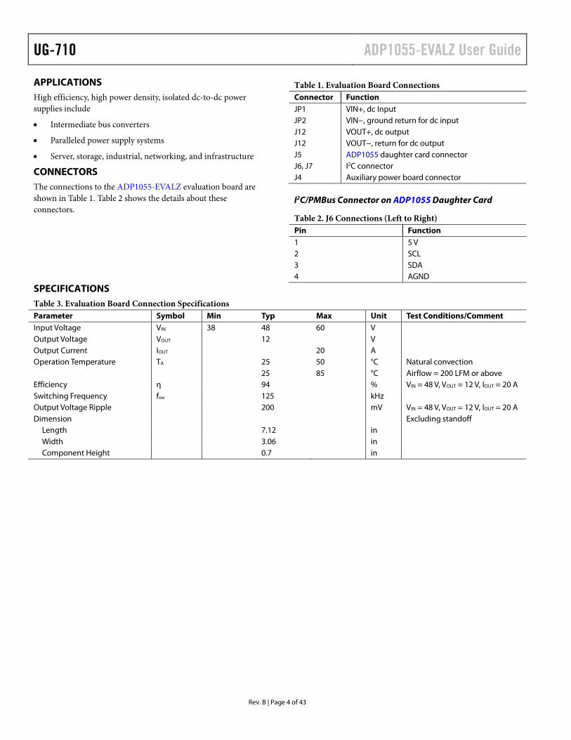
CONNECTORS The connections to the ADP1055-EVALZ evaluation board are shown in Table 1. Table 2 shows the details about these connectors.
Table 1. Evaluation Board Connections Connector Function JP1 VIN+, dc Input JP2 VIN−, ground return for dc input J12 VOUT+, dc output J12 VOUT−, return for dc output J5 ADP1055 daughter card connector J6, J7 I2C connector J4 Auxiliary power board connector
I2C/PMBus Connector on ADP1055 Daughter Card
Table 2. J6 Connections (Left to Right) Pin Function 1 5 V 2 SCL 3 SDA 4 AGND
SPECIFICATIONS Table 3. Evaluation Board Connection Specifications Parameter Symbol Min Typ Max Unit Test Conditions/Comment Input Voltage VIN 38 48 60 V Output Voltage VOUT 12 V Output Current IOUT 20 A Operation Temperature TA 25 50 °C Natural convection 25 85 °C Airflow = 200 LFM or above Efficiency η 94 % VIN = 48 V, VOUT = 12 V, IOUT = 20 A Switching Frequency fsw 125 kHz Output Voltage Ripple 200 mV VIN = 48 V, VOUT = 12 V, IOUT = 20 A Dimension Excluding standoff
Length 7.12 in Width 3.06 in Component Height 0.7 in
Rev. B | Page 4 of 43

ADP1055-EVALZ User Guide UG-710
Rev. B | Page 5 of 43
GETTING STARTED CAUTION This evaluation board uses high voltages and currents. Extreme caution should be taken, especially on the primary side, to ensure your safety. It is strongly advised to switch off the evaluation board when not in use. A current limited, isolated dc source is recommended at input.
HARDWARE Evaluation Equipment
DC power supply capable of 38 V dc to 60 V dc, 10 A. Electronic load capable of 12 V, 25 A input. Oscilloscope capable of 500 MHz bandwidth or above,
2 to 4 channel. PC with Microsoft Windows® XP (32 bit), or Vista (32 bit),
Windows 7 (32/64 bit), and Windows 8 (32 bit).
Precision digital multimeters (HP34401 or equivalent). USB to I2C connector ADP-I2C-USB-Z as shown in
Figure 5. This must be ordered from Analog Devices. Portable DMM (Fluke Corp.) for measuring up to 25 A dc
current (optional).
Evaluation Board Configurations
The evaluation board is preconfigured with the default settings to operate the power supply at the rated load. No additional configuration is necessary other than to turn on the hardware PSON switch. Additional software configuration may be necessary to change thresholds and parameters.
Hardware Connection
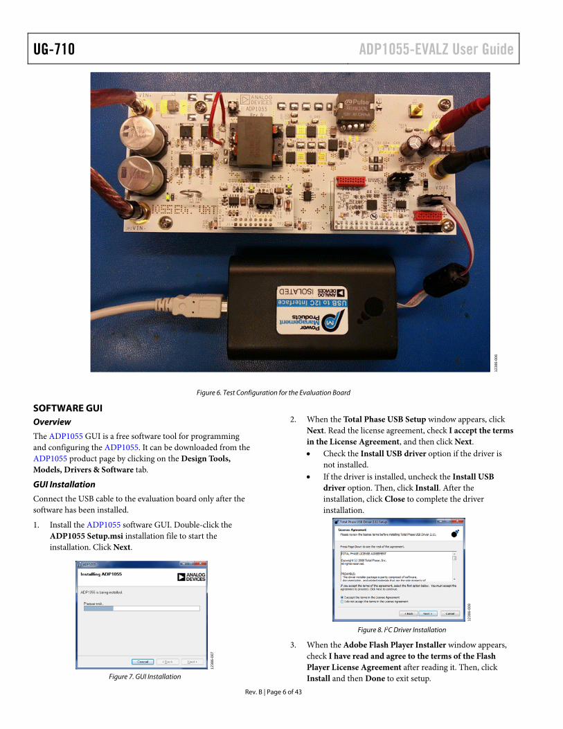
Figure 6 shows an example of the test configuration of the hardware.
1238
6-00
5
Figure 5. USB to I2C Interface Connector ADP-I2C-USB-Z
UG-710 ADP1055-EVALZ User Guide
Rev. B | Page 6 of 43
1238
6-00
6
Figure 6. Test Configuration for the Evaluation Board
SOFTWARE GUI Overview
The ADP1055 GUI is a free software tool for programming and configuring the ADP1055. It can be downloaded from the ADP1055 product page by clicking on the Design Tools, Models, Drivers & Software tab.
GUI Installation
Connect the USB cable to the evaluation board only after the software has been installed.
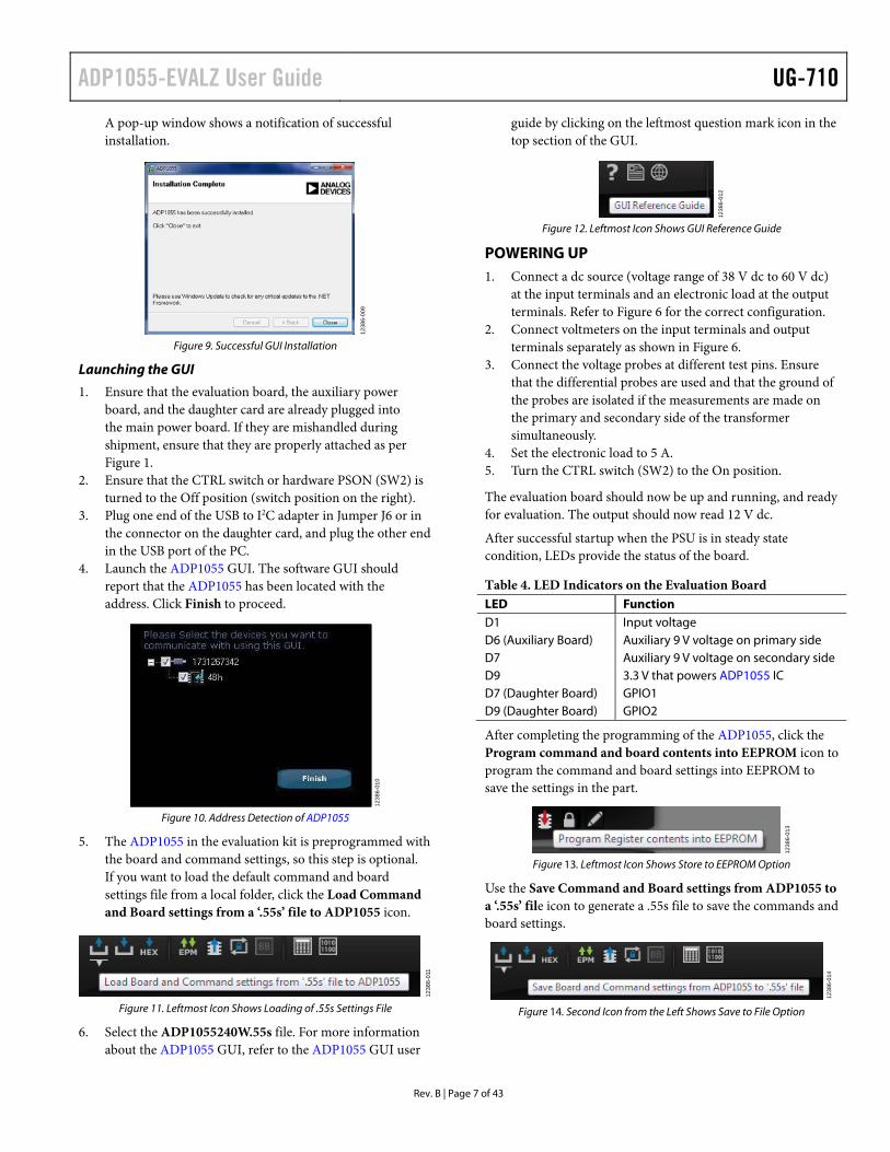
1. Install the ADP1055 software GUI. Double-click the ADP1055 Setup.msi installation file to start the installation. Click Next.
1238
6-00
7
Figure 7. GUI Installation
2. When the Total Phase USB Setup window appears, click Next. Read the license agreement, check I accept the terms in the License Agreement, and then click Next. Check the Install USB driver option if the driver is
not installed. If the driver is installed, uncheck the Install USB
driver option. Then, click Install. After the installation, click Close to complete the driver installation.
1238
6-00
8
Figure 8. I2C Driver Installation
3. When the Adobe Flash Player Installer window appears, check I have read and agree to the terms of the Flash Player License Agreement after reading it. Then, click Install and then Done to exit setup.
ADP1055-EVALZ User Guide UG-710
Rev. B | Page 7 of 43
A pop-up window shows a notification of successful installation.
1238
6-00
9
Figure 9. Successful GUI Installation
Launching the GUI
1. Ensure that the evaluation board, the auxiliary power board, and the daughter card are already plugged into the main power board. If they are mishandled during shipment, ensure that they are properly attached as per Figure 1.
2. Ensure that the CTRL switch or hardware PSON (SW2) is turned to the Off position (switch position on the right).
3. Plug one end of the USB to I2C adapter in Jumper J6 or in the connector on the daughter card, and plug the other end in the USB port of the PC.
4. Launch the ADP1055 GUI. The software GUI should report that the ADP1055 has been located with the address. Click Finish to proceed.
1238
6-01
0
Figure 10. Address Detection of ADP1055
5. The ADP1055 in the evaluation kit is preprogrammed with the board and command settings, so this step is optional. If you want to load the default command and board settings file from a local folder, click the Load Command and Board settings from a ‘.55s’ file to ADP1055 icon.
1238
6-01
1
Figure 11. Leftmost Icon Shows Loading of .55s Settings File
6. Select the ADP1055240W.55s file. For more information about the ADP1055 GUI, refer to the ADP1055 GUI user
guide by clicking on the leftmost question mark icon in the top section of the GUI.
1238
6-01
2
Figure 12. Leftmost Icon Shows GUI Reference Guide
POWERING UP 1. Connect a dc source (voltage range of 38 V dc to 60 V dc)
at the input terminals and an electronic load at the output terminals. Refer to Figure 6 for the correct configuration.
2. Connect voltmeters on the input terminals and output terminals separately as shown in Figure 6.
3. Connect the voltage probes at different test pins. Ensure that the differential probes are used and that the ground of the probes are isolated if the measurements are made on the primary and secondary side of the transformer simultaneously.
4. Set the electronic load to 5 A. 5. Turn the CTRL switch (SW2) to the On position.
The evaluation board should now be up and running, and ready for evaluation. The output should now read 12 V dc.
After successful startup when the PSU is in steady state condition, LEDs provide the status of the board.
Table 4. LED Indicators on the Evaluation Board LED Function D1 Input voltage D6 (Auxiliary Board) Auxiliary 9 V voltage on primary side D7 Auxiliary 9 V voltage on secondary side D9 3.3 V that powers ADP1055 IC D7 (Daughter Board) GPIO1 D9 (Daughter Board) GPIO2
After completing the programming of the ADP1055, click the Program command and board contents into EEPROM icon to program the command and board settings into EEPROM to save the settings in the part.
1238
6-01
3
Figure 13. Leftmost Icon Shows Store to EEPROM Option
Use the Save Command and Board settings from ADP1055 to a ‘.55s’ file icon to generate a .55s file to save the commands and board settings.
1238
6-01
4
Figure 14. Second Icon from the Left Shows Save to File Option
UG-710 ADP1055-EVALZ User Guide
Rev. B | Page 8 of 43
1238
6-01
5
Figure 15. Main Setup Window of the ADP1055 GUI
1238
6-01
6
Figure 16. Monitor Window in the GUI
For more information on the board settings, refer to the GUI reference guide (see Figure 12).
ADP1055-EVALZ User Guide UG-710
Rev. B | Page 9 of 43
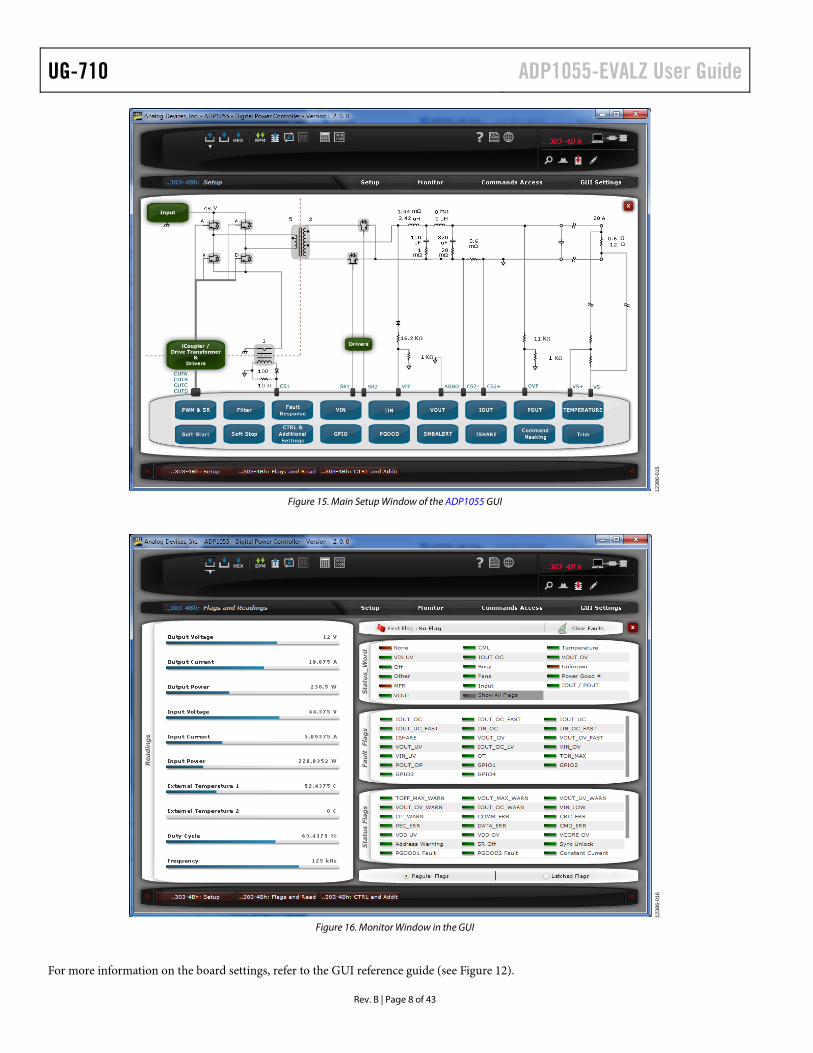
EVALUATING THE ADP1055 The goal of this user guide is to familiarize you with the GUI and to describe the flexibility available with the extensive programming options provided by the ADP1055. Several test points on the evaluation board allow easy monitoring of the various signals. You can use the GUI software to program multiple responses for the various fault conditions. The following sections provides a description of the typical features and results realized when evaluating this device.
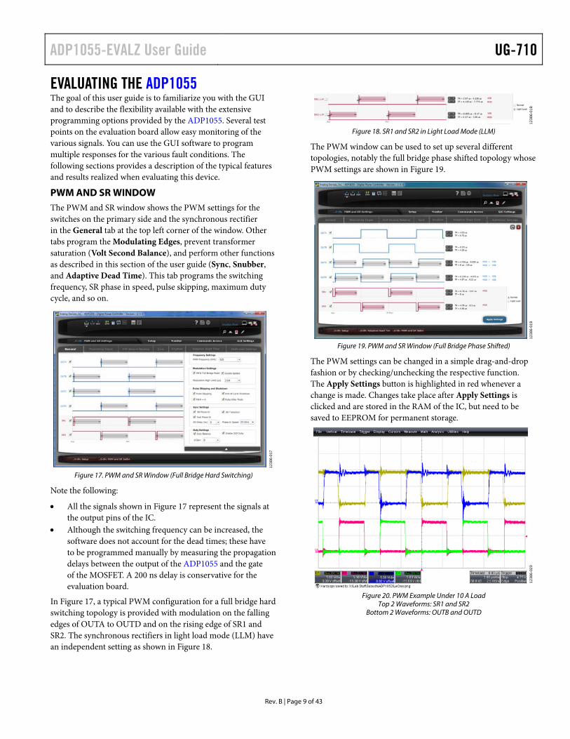
PWM AND SR WINDOW The PWM and SR window shows the PWM settings for the switches on the primary side and the synchronous rectifier in the General tab at the top left corner of the window. Other tabs program the Modulating Edges, prevent transformer saturation (Volt Second Balance), and perform other functions as described in this section of the user guide (Sync, Snubber, and Adaptive Dead Time). This tab programs the switching frequency, SR phase in speed, pulse skipping, maximum duty cycle, and so on.
1238
6-01
7
Figure 17. PWM and SR Window (Full Bridge Hard Switching)
Note the following:
All the signals shown in Figure 17 represent the signals at the output pins of the IC.
Although the switching frequency can be increased, the software does not account for the dead times; these have to be programmed manually by measuring the propagation delays between the output of the ADP1055 and the gate of the MOSFET. A 200 ns delay is conservative for the evaluation board.
In Figure 17, a typical PWM configuration for a full bridge hard switching topology is provided with modulation on the falling edges of OUTA to OUTD and on the rising edge of SR1 and SR2. The synchronous rectifiers in light load mode (LLM) have an independent setting as shown in Figure 18.
1238
6-01
8
Figure 18. SR1 and SR2 in Light Load Mode (LLM)
The PWM window can be used to set up several different topologies, notably the full bridge phase shifted topology whose PWM settings are shown in Figure 19.
1238
6-01
9
Figure 19. PWM and SR Window (Full Bridge Phase Shifted)
The PWM settings can be changed in a simple drag-and-drop fashion or by checking/unchecking the respective function. The Apply Settings button is highlighted in red whenever a change is made. Changes take place after Apply Settings is clicked and are stored in the RAM of the IC, but need to be saved to EEPROM for permanent storage.
1238
6-02
0
Figure 20. PWM Example Under 10 A Load
Top 2 Waveforms: SR1 and SR2 Bottom 2 Waveforms: OUTB and OUTD
UG-710 ADP1055-EVALZ User Guide
Rev. B | Page 10 of 43
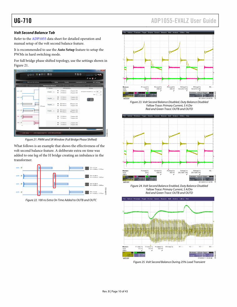
Volt Second Balance Tab
Refer to the ADP1055 data sheet for detailed operation and manual setup of the volt second balance feature.
It is recommended to use the Auto Setup feature to setup the PWMs in hard switching mode.
For full bridge phase shifted topology, use the settings shown in Figure 21.
1238
6-02
1
Figure 21. PWM and SR Window (Full Bridge Phase Shifted)
What follows is an example that shows the effectiveness of the volt second balance feature. A deliberate extra on time was added to one leg of the H bridge creating an imbalance in the transformer.
1238
6-02
2
Figure 22. 100 ns Extra On Time Added to OUTB and OUTC
1238
6-02
3
Figure 23. Volt Second Balance Disabled, Duty Balance Disabled
Yellow Trace: Primary Current, 5 A Div Red and Green Trace: OUTB and OUTD
1238
6-02
4
Figure 24. Volt Second Balance Enabled, Duty Balance Disabled
Yellow Trace: Primary Current, 5 A/Div Red and Green Trace: OUTB and OUTD
1238
6-02
5
Figure 25. Volt Second Balance During 25% Load Transient

ADP1055-EVALZ User Guide UG-710
Rev. B | Page 11 of 43
Synchronization Tab
1238
6-02
6
Figure 26. Phase Delay Between SYNC Pulse and PWM Timing
The phase delay, that is, the alignment of the PWM set (OUTA to OUTD and SR1, SR2) with synchronization pulse can be programmed in this tab. For a full description of the SYNC function, refer to the data sheet.
The SYNC settings can be changed in a simple drag-and-drop fashion. The Apply Settings button is highlighted in red whenever a change is made. Changes take place after Apply Settings is clicked and are stored in the RAM of the IC, but need to be saved to EEPROM for permanent storage.
Adaptive Dead Time (ADT) Tab
See the ADP1055 data sheet for detailed operation of the ADT feature. In the example provided in this section, the GUI has programmed the SR edges to become narrower when the load has decreased to increase light load efficiency.
The ADT settings can be changed in a simple drag-and-drop fashion or by merely checking/unchecking the respective function. The Apply Settings button is highlighted in red whenever a change is made. Changes take place after the Apply Settings is clicked and are stored in the RAM of the IC, but need to be saved to EEPROM for permanent storage.
1238
6-02
7
Figure 27. ADT Window
Things to Try
1. Set up PWMs for additional topologies, such as active clamp, isolated boost, and so on.
2. Use the SYNC feature of the ADP1055 to synchronize to an external frequency.
CTRL AND PSON WINDOW In this window, the configuration of the hardware and software PSON can be programmed. Additional settings, such as the extended slave address selection, voltage overshoot (regulation timeout speed) and write protect mode, can be selected.
1238
6-02
8
Figure 28. PSON Window
The settings can be changed by simply toggling the switches or by selecting the suitable option from the drop-down menu. Changes take place immediately and are stored in the RAM of the IC, but need to be saved to EEPROM for permanent storage.
Overshoot Protection (Regulation Timeout) and DIP Test
The ADP1055 provides an overshoot protection feature (regulation timeout). If enabled, a soft-start is run from the precharge function whenever the output voltage is out of regulation for a certain number of switching periods. This prevents the system from overshooting in output voltage, such as in the case of a DIP test where the input voltage dips below nominal and puts the output voltage out of regulation. In Figure 29, the PSU has been given a PSON signal several minutes before the input voltage is above the VIN_UV threshold.
1238
6-02
9
Figure 29. Demonstration of Overshoot Protection at No Load
Green Trace: Output Voltage Blue Trace: Input Voltage
Red Trace: PWM
UG-710 ADP1055-EVALZ User Guide
Rev. B | Page 12 of 43
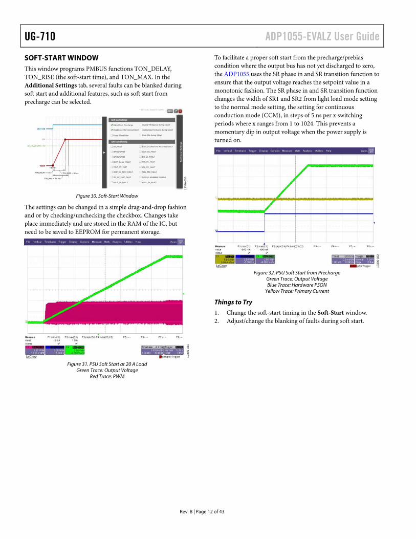
SOFT-START WINDOW This window programs PMBUS functions TON_DELAY, TON_RISE (the soft-start time), and TON_MAX. In the Additional Settings tab, several faults can be blanked during soft start and additional features, such as soft start from precharge can be selected.
1238
6-03
0
Figure 30. Soft-Start Window
The settings can be changed in a simple drag-and-drop fashion and or by checking/unchecking the checkbox. Changes take place immediately and are stored in the RAM of the IC, but need to be saved to EEPROM for permanent storage.
1238
6-03
1
Figure 31. PSU Soft Start at 20 A Load
Green Trace: Output Voltage Red Trace: PWM
To facilitate a proper soft start from the precharge/prebias condition where the output bus has not yet discharged to zero, the ADP1055 uses the SR phase in and SR transition function to ensure that the output voltage reaches the setpoint value in a monotonic fashion. The SR phase in and SR transition function changes the width of SR1 and SR2 from light load mode setting to the normal mode setting, the setting for continuous conduction mode (CCM), in steps of 5 ns per x switching periods where x ranges from 1 to 1024. This prevents a momentary dip in output voltage when the power supply is turned on.
1238
6-03
2
Figure 32. PSU Soft Start from Precharge
Green Trace: Output Voltage Blue Trace: Hardware PSON
Yellow Trace: Primary Current
Things to Try
1. Change the soft-start timing in the Soft-Start window. 2. Adjust/change the blanking of faults during soft start.
ADP1055-EVALZ User Guide UG-710
Rev. B | Page 13 of 43
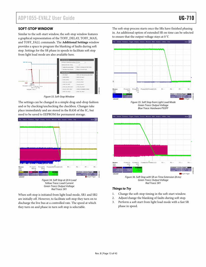
SOFT-STOP WINDOW Similar to the soft-start window, the soft-stop window features a graphical representation of the TOFF_DELAY, TOFF_MAX, and TOFF_FALL commands. The Additional Settings window provides a space to program the blanking of faults during soft stop. Settings for the SR phase in speeds to facilitate soft stop from light load mode are also available here.
1238
6-03
3
Figure 33. Soft-Stop Window
The settings can be changed in a simple drag-and-drop fashion and or by checking/unchecking the checkbox. Changes take place immediately and are stored in the RAM of the IC, but need to be saved to EEPROM for permanent storage.
1238
6-03
4
Figure 34. Soft Stop at 20 A Load
Yellow Trace: Load Current Green Trace: Output Voltage
Red Trace: SR1
When soft stop is initiated from light load mode, SR1 and SR2 are initially off. However, to facilitate soft stop they turn on to discharge the live bus at a controlled rate. The speed at which they turn on and phase in turn soft stop is selectable.
The soft-stop process starts once the SRs have finished phasing in. An additional option of extended SR on time can be selected to ensure that the output voltage stays at 0 V.
1238
6-03
5
Figure 35. Soft Stop from Light Load Mode
Green Trace: Output Voltage Blue Trace: Hardware PSOFF
1238
6-03
6
Figure 36. Soft Stop with SR on Time Extension (8 ms)
Green Trace: Output Voltage Red Trace: SR1
Things to Try
1. Change the soft-stop timing in the soft-start window. 2. Adjust/change the blanking of faults during soft stop. 3. Perform a soft start from light load mode with a fast SR
phase in speed.
UG-710 ADP1055-EVALZ User Guide
Rev. B | Page 14 of 43
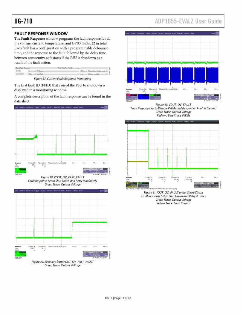
FAULT RESPONSE WINDOW The Fault Response window programs the fault response for all the voltage, current, temperature, and GPIO faults, 22 in total. Each fault has a configuration with a programmable debounce time, and the response to the fault followed by the delay time between consecutive soft starts if the PSU is shutdown as a result of the fault action.
1238
6-03
7
Figure 37. Current Fault Response Monitoring
The first fault ID (FFID) that caused the PSU to shutdown is displayed in a monitoring window.
A complete description of the fault response can be found in the data sheet.
1238
6-03
8
Figure 38. VOUT_OV_FAST_FAULT
Fault Response Set to Shut Down and Retry Indefinitely Green Trace: Output Voltage
1238
6-03
9
Figure 39. Recovery from VOUT_OV_FAST_FAULT
Green Trace: Output Voltage
1238
6-04
0
Figure 40. VOUT_OV_FAULT
Fault Response Set to Disable PWMs and Retry when Fault is Cleared Green Trace: Output Voltage
Red and Blue Trace: PWMs
1238
6-04
1
Figure 41. IOUT_OC_FAULT under Short-Circuit
Fault Response Set to Shut Down and Retry 4 Times Green Trace: Output Voltage Yellow Trace: Load Current
ADP1055-EVALZ User Guide UG-710
Rev. B | Page 15 of 43
1238
6-04
2
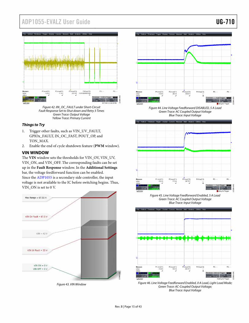
Figure 42. IIN_OC_FAULT under Short-Circuit
Fault Response Set to Shut down and Retry 3 Times Green Trace: Output Voltage
Yellow Trace: Primary Current
Things to Try
1. Trigger other faults, such as VIN_UV_FAULT, GPIOx_FAULT, IN_OC_FAST, POUT_OP, and TON_MAX.
2. Enable the end of cycle shutdown feature (PWM window).
VIN WINDOW The VIN window sets the thresholds for VIN_OV, VIN_UV, VIN_ON, and VIN_OFF. The corresponding faults can be set up in the Fault Response window. In the Additional Settings bar, the voltage feedforward function can be enabled. Since the ADP1055 is a secondary side controller, the input voltage is not available to the IC before switching begins. Thus, VIN_ON is set to 0 V.
1238
6-04
3
Figure 43. VIN Window
1238
6-04
4
Figure 44. Line Voltage Feedforward DISABLED, 5 A Load
Green Trace: AC Coupled Output Voltage Blue Trace: Input Voltage
1238
6-04
5
Figure 45. Line Voltage Feedforward Enabled, 5 A Load
Green Trace: AC Coupled Output Voltage Blue Trace: Input Voltage
1238
6-04
6
Figure 46. Line Voltage Feedforward Enabled, 0 A Load, Light Load Mode;
Green Trace: AC-Coupled Output Voltage; Blue Trace: Input Voltage
UG-710 ADP1055-EVALZ User Guide
Rev. B | Page 16 of 43
1238
6-04
7
Figure 47. Voltage Line Feedforward;
Red Trace: Input Voltage 10 V/Div; Green Trace: AC-Coupled Output Voltage;
Blue and Yellow Traces: OUTB and OUTC PWMs
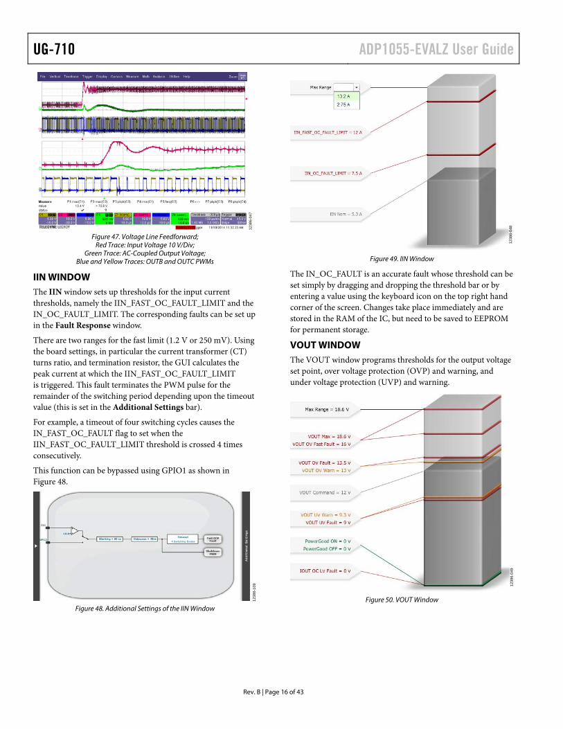
IIN WINDOW The IIN window sets up thresholds for the input current thresholds, namely the IIN_FAST_OC_FAULT_LIMIT and the IN_OC_FAULT_LIMIT. The corresponding faults can be set up in the Fault Response window.
There are two ranges for the fast limit (1.2 V or 250 mV). Using the board settings, in particular the current transformer (CT) turns ratio, and termination resistor, the GUI calculates the peak current at which the IIN_FAST_OC_FAULT_LIMIT is triggered. This fault terminates the PWM pulse for the remainder of the switching period depending upon the timeout value (this is set in the Additional Settings bar).
For example, a timeout of four switching cycles causes the IN_FAST_OC_FAULT flag to set when the IIN_FAST_OC_FAULT_LIMIT threshold is crossed 4 times consecutively.
This function can be bypassed using GPIO1 as shown in Figure 48.
1238
6-10
9
Figure 48. Additional Settings of the IIN Window
1238
6-04
8
Figure 49. IIN Window
The IN_OC_FAULT is an accurate fault whose threshold can be set simply by dragging and dropping the threshold bar or by entering a value using the keyboard icon on the top right hand corner of the screen. Changes take place immediately and are stored in the RAM of the IC, but need to be saved to EEPROM for permanent storage.
VOUT WINDOW The VOUT window programs thresholds for the output voltage set point, over voltage protection (OVP) and warning, and under voltage protection (UVP) and warning.
1238
6-04
9
Figure 50. VOUT Window

ADP1055-EVALZ User Guide UG-710
Rev. B | Page 17 of 43
1238
6-05
0
Figure 51. Additional Settings of VOUT Window
The settings can be changed in a simple drag-and-drop fashion and or by selecting the value from the combo box. Changes to the VOUT_DROOP and VOUT_TRANSITION value take place after the button on the right side next to the text box is clicked. Other changes take place immediately and are stored in the RAM of the IC, but need to be saved to EEPROM for permanent storage.
1238
6-05
1
OU
TPU
T VO
LTA
GE
(V)
DEL
TA =
GU
I-MEA
SUR
ED (m
V)
LOAD CURRENT (A)
12.00 4
2
0
0 1 2 3 4 5 6 7 8 9
–2
–4
–6
–8
–10
–12
–14
–16
12.04
GUIMEASUREDDELTA
12.02
12.00
11.98
11.96
11.94
11.92
11.90
Figure 52. VOUT_DROOP = 10 mV/A
1238
6-05
2
Figure 53. Output Voltage Ripple, 20 A Load
Green Trace: AC Coupled Output Voltage
IOUT WINDOW The IOUT window sets thresholds for the output current. Thresholds for output over current, under current, and constant current can be programmed via this window.
1238
6-05
3
Figure 54. IOUT Window
1238
6-05
4
Figure 55. Light Load Settings in IOUT Window
Additionally, settings for the light load mode can also be programmed in this window through the Light Load Settings bar on the right side. The thresholds can be programmed from the drop-down list. The deep light load mode can be enabled, if necessary.
It is recommended to use the manufacturer specific mode with the maximum slew rate to control (decrease) the output voltage when the load current crosses the constant current threshold. The constant current threshold is set to a percentage (for example, ±3.125% or ±12.5%) of the IOUT_OC_FAULT_LIMIT.
UG-710 ADP1055-EVALZ User Guide
Rev. B | Page 18 of 43
1238
6-05
5
Figure 56. IOUT_OC_FAULT
PSU is Set to Enter Constant Current Mode at 27 A. Fault Response Set to Wait for a Debounce of 5 Seconds, Shutdown, and Retry Indefinitely.
Green Trace: Output Voltage Yellow Trace: Load Current
1238
6-05
6
Figure 57. Constant Current Mode in a Load Resistor
Green Trace: Output Voltage Yellow Trace: Load Current
1238
6-05
7
Figure 58. Additional Settings in IOUT Window
In the Additional Settings bar, the cycle by cycle protection (over current and reverse current) can be set. Also, the constant current averaging rate and the slew rate can be selected.
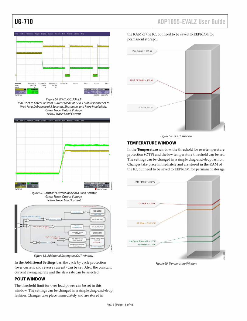
POUT WINDOW The threshold limit for over load power can be set in this window. The settings can be changed in a simple drag-and-drop fashion. Changes take place immediately and are stored in
the RAM of the IC, but need to be saved to EEPROM for permanent storage.
1238
6-05
8
Figure 59. POUT Window
TEMPERATURE WINDOW In the Temperature window, the threshold for overtemperature protection (OTP) and the low temperature threshold can be set. The settings can be changed in a simple drag-and-drop fashion. Changes take place immediately and are stored in the RAM of the IC, but need to be saved to EEPROM for permanent storage.
1238
6-05
9
Figure 60. Temperature Window
ADP1055-EVALZ User Guide UG-710
Rev. B | Page 19 of 43
PGOOD AND GPIO WINDOWS The PGOOD and GPIO windows go hand in hand. Several flags, such as IOUT_OC_FAULT and VOUT_OV, can be set into PGOOD1 and PGOOD2 which are internal signals. These can be routed to hardware pins GPIO1 to GPIO4 in the GPIO window.
1238
6-06
0
Figure 61. Additional Settings in IOUT Window
The GPIO window configures the GPIO1 to GPIO4 pins either as an input or as an output. If selected as an output, the pin can output a logic combination of PGOOD1 and PGOOD2. If selected as an input, then it acts as a digital input whereupon a GPIOx fault can be triggered.
1238
6-06
1
Figure 62. GPIO Window
There are several logic operations available for programming the output as shown in Figure 63.
1238
6-06
2
Figure 63. Logic Options for GPIO
32-BIT KEYCODE The ADP1055 has a 32-bit password protection and extended command masking set.
1238
6-06
3
Figure 64. Change Keycode Icon (Sixth from the Left)
1238
6-06
4
Figure 65. Example of Changing the Keycode Using a Pneumonic
for Negative Feedback in Signed Binary Numbers
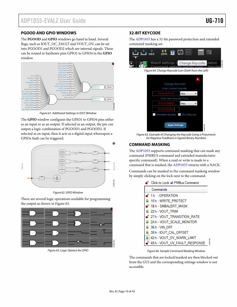
COMMAND MASKING The ADP1055 supports command masking that can mask any command (PMBUS command and extended manufacturer specific command). When a read or write is made to a command that is masked, the ADP1055 returns with a NACK.
Commands can be masked in the command masking window by simply clicking on the lock next to the command.
1238
6-06
5
Figure 66. Sample Command Masking Window
The commands that are locked/masked are then blocked out from the GUI and the corresponding settings window is not accessible.
UG-710 ADP1055-EVALZ User Guide
Rev. B | Page 20 of 43
1238
6-06
6
Figure 67. Lock Masked Commands Icon (Rightmost Icon)
ACTIVE CLAMP SNUBBER GPIO3 and GPIO4 can be configured to have the special function of an active clamp snubber. In this feature, GPIO3 and GPIO4 act as PWM signals that are triggered off a reference PWM which is either
Falling edge of SR1 and SR2 or Falling edge of OUTC and OUTD (that is, rising edge of
OUTC and OUTD)
1238
6-06
7
Figure 68. Active Clamp Options Selected in PWM Window, Snubber Tab
The active snubber function has additional options of a programmable on time and a delay from the reference PWM. A complete description of the active snubber function is available in the data sheet.
1238
6-06
8
Figure 69. Active Clamp Option in Evaluation Board
1238
6-06
9
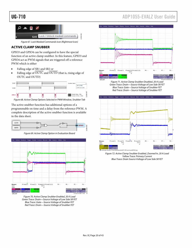
Figure 70. Active Clamp Snubber Enabled, 20 A Load
Green Trace: Drain—Source Voltage of Low Side SR FET Blue Trace: Gate—Source Voltage of Snubber FET Red Trace: Drain—Source Voltage of Snubber FET
1238
6-07
0
Figure 71. Active Clamp Snubber Disabled, 20 A Load
Green Trace: Drain—Source Voltage of Low Side SR FET Blue Trace: Gate—Source Voltage of Snubber FET Red Trace: Drain—Source Voltage of Snubber FET
1238
6-07
1
Figure 72. Active Clamp Snubber Enabled, Zoomed In, 20 A Load
Yellow Trace: Primary Current Blue Trace: Drain Source Voltage of Low Side SR FET
ADP1055-EVALZ User Guide UG-710
Rev. B | Page 21 of 43
1238
6-07
2
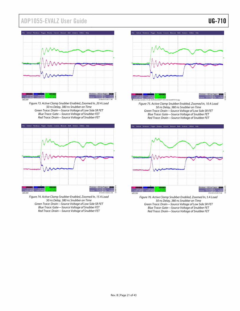
Figure 73. Active Clamp Snubber Enabled, Zoomed In, 20 A Load
50 ns Delay, 380 ns Snubber on Time Green Trace: Drain—Source Voltage of Low Side SR FET
Blue Trace: Gate—Source Voltage of Snubber FET Red Trace: Drain—Source Voltage of Snubber FET
1238
6-07
3
Figure 74. Active Clamp Snubber Enabled, Zoomed In, 15 A Load
50 ns Delay, 380 ns Snubber on Time Green Trace: Drain—Source Voltage of Low Side SR FET
Blue Trace: Gate—Source Voltage of Snubber FET Red Trace: Drain—Source Voltage of Snubber FET
1238
6-07
4
Figure 75. Active Clamp Snubber Enabled, Zoomed In, 10 A Load
50 ns Delay, 380 ns Snubber on Time Green Trace: Drain—Source Voltage of Low Side SR FET
Blue Trace: Gate—Source Voltage of Snubber FET Red Trace: Drain—Source Voltage of Snubber FET
1238
6-07
5
Figure 76. Active Clamp Snubber Enabled, Zoomed In, 5 A Load
50 ns Delay, 380 ns Snubber on Time Green Trace: Drain—Source Voltage of Low Side SR FET
Blue Trace: Gate—Source Voltage of Snubber FET Red Trace: Drain—Source Voltage of Snubber FET

UG-710 ADP1055-EVALZ User Guide
Rev. B | Page 22 of 43
DIGITAL CONTROL LOOP Control Loop Configuration
The control loop configuration procedures can be shown as a series of three steps.
1. The board parameters are set, including topology, turn ratio of main transformer, output LC filter and output voltage feedback network. Using this inform-ation, the ADP1055 generates the Bode plots of LC filter and feedback network.
2. The switching frequency is determined in the PWM settings window. Changing of the switching frequency changes the low frequency gain and the third pole position.
3. You can start to place the zeros and poles, and set the low frequency gain and high frequency gain of the Type-III compensator, based on the stability rules.
Using the loop analyzer, you can validate the programmed control loop as shown in Figure 78. For an easy test on the control loop, the signal from loop analyzer can be injected in J11and TP26 in the schematic.
1238
6-07
6
Figure 77. Digital Filter Settings Window
The double update rate feature of the ADP1055 greatly increases the ability to push the bandwidth to higher limits while still retaining a good phase margin.
1238
6-07
7
Figure 78. Control Loop Test by AP300 Loop Analyzer
(Double Update Rate Enabled) Crossover Frequency is 5.41kHz
Phase Margin is 60° Gain Margin is 22 dB
1238
6-07
8
Figure 79. Digital Filter Settings Window
Optimized Filter to Provide Better Crossover Frequency
1238
6-07
9
Figure 80. Control Loop Test by AP300 Loop Analyzer
(Double Update Rate Enabled) Crossover Frequency is 9.08 kHz
Phase Margin is 58° Gain Margin is 22 dB
ADP1055-EVALZ User Guide UG-710
Rev. B | Page 23 of 43
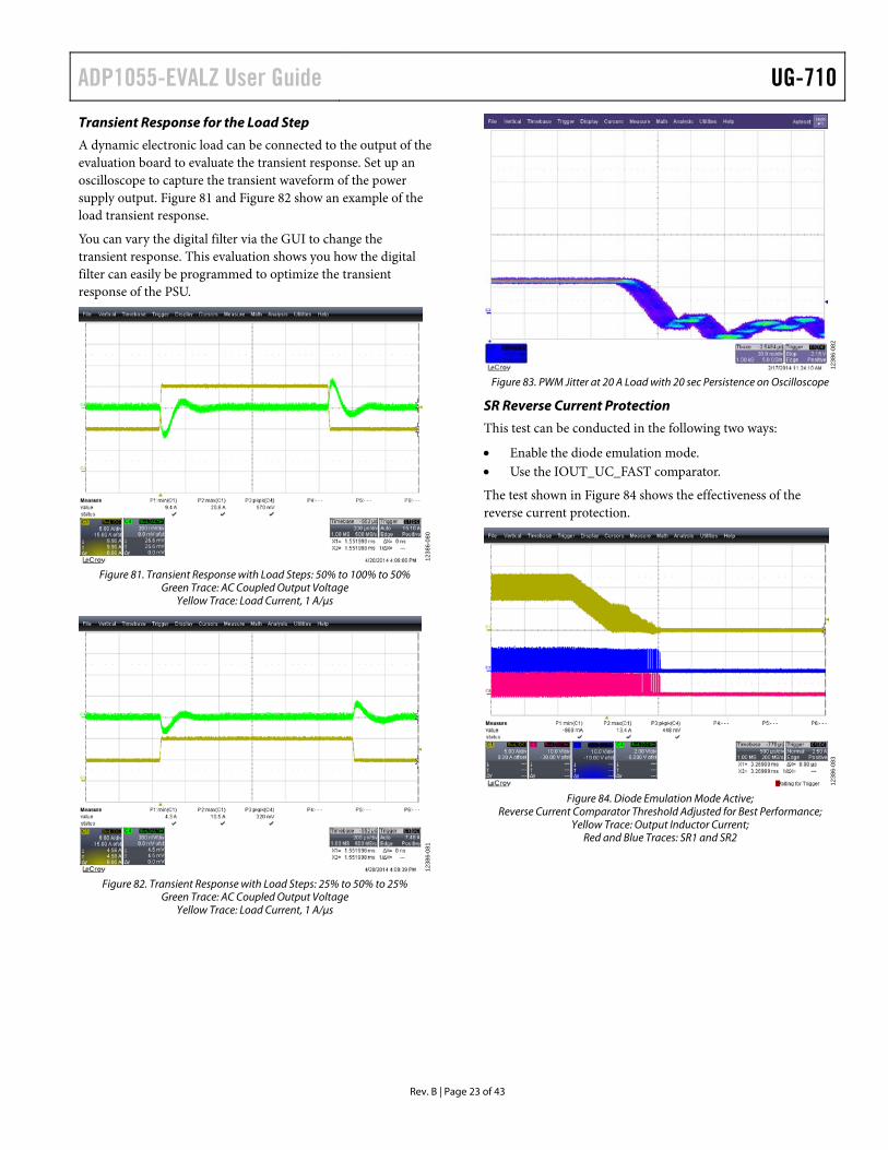
Transient Response for the Load Step
A dynamic electronic load can be connected to the output of the evaluation board to evaluate the transient response. Set up an oscilloscope to capture the transient waveform of the power supply output. Figure 81 and Figure 82 show an example of the load transient response.
You can vary the digital filter via the GUI to change the transient response. This evaluation shows you how the digital filter can easily be programmed to optimize the transient response of the PSU.
1238
6-08
0
Figure 81. Transient Response with Load Steps: 50% to 100% to 50%
Green Trace: AC Coupled Output Voltage Yellow Trace: Load Current, 1 A/μs
1238
6-08
1
Figure 82. Transient Response with Load Steps: 25% to 50% to 25%
Green Trace: AC Coupled Output Voltage Yellow Trace: Load Current, 1 A/μs
1238
6-08
2
Figure 83. PWM Jitter at 20 A Load with 20 sec Persistence on Oscilloscope
SR Reverse Current Protection
This test can be conducted in the following two ways:
Enable the diode emulation mode. Use the IOUT_UC_FAST comparator.
The test shown in Figure 84 shows the effectiveness of the reverse current protection.
1238
6-08
3
Figure 84. Diode Emulation Mode Active;
Reverse Current Comparator Threshold Adjusted for Best Performance; Yellow Trace: Output Inductor Current;
Red and Blue Traces: SR1 and SR2

UG-710 ADP1055-EVALZ User Guide
Rev. B | Page 24 of 43
1238
6-08
4
Figure 85. Diode Emulation Mode Active; Threshold Adjusted for Best
Performance; Waveform Shows that SR1 and SR2 Move from CCM to Diode Emulation Mode Instantly;
Yellow Trace: Output Inductor Current; Red and Blue Traces: SR1 and SR2
Figure 86. IOUT_UC_FAST_FAULT; Output Inductor Shorted to Ground;
The Reverse Current Comparator Threshold Adjusted for Best Performance; Yellow Trace: Output Inductor Current;
Red and Blue Traces: SR1 and SR2; Green Trace: Synchronous Rectifier Drain Voltage
Light Load Efficiency Optimization
The ADP1055 can be programmed to optimize performance when the output current drops below a certain level. The light load and deep light load mode thresholds are set in a manner to reduce losses and increase efficiency. A hysteresis for light load mode and deep light load mode is provided on the thresholds to avoid oscillations. The thresholds for light load mode and deep light load mode can also be programmed in the IOUT setting window as shown in Figure 87.
Figure 87. Light Load Mode and Deep Light Load Mode Thresholds
When operating in light load mode or deep light load mode, the light load mode flag is set as shown in the Monitor tab. In both situations, the light load filter settings are used. In combination with the pulse skipping function, the standby power consumption can be reduced.
ADP1055-EVALZ User Guide UG-710
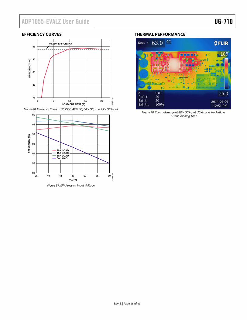
EFFICIENCY CURVES
75
80
85
90
95
0 5 10 15 20
EFFI
CIE
NC
Y (%
)
LOAD CURRENT (A)
94.18% EFFICIENCY
1238
6-10
4
Figure 88. Efficiency Curve at 36 V DC, 48 V DC, 60 V DC, and 75 V DC Input
89
90
91
92
93
94
95
36 40 44 48 52 56 60
EFFI
CIE
NC
Y (%
)
VIN (V)
20A LOAD15A LOAD10A LOAD5A LOAD
1238
6-10
5
Figure 89. Efficiency vs. Input Voltage
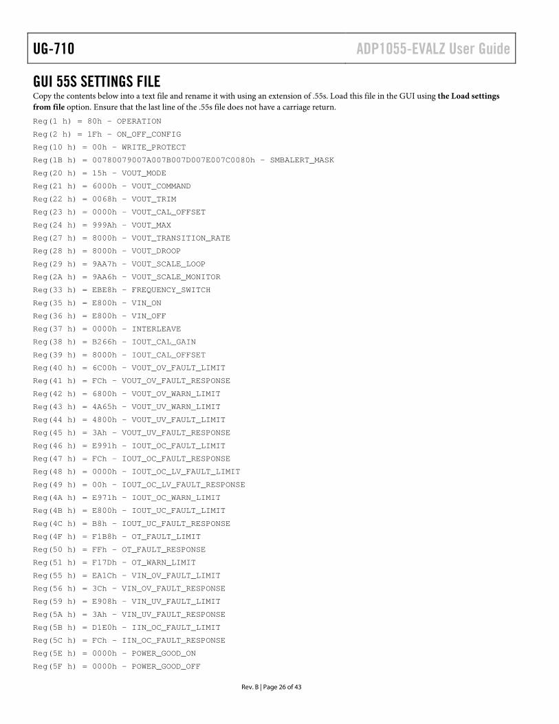
THERMAL PERFORMANCE
Figure 90. Thermal Image at 48 V DC Input, 20 A Load, No Airflow,
1 Hour Soaking Time
Rev. B | Page 25 of 43
UG-710 ADP1055-EVALZ User Guide
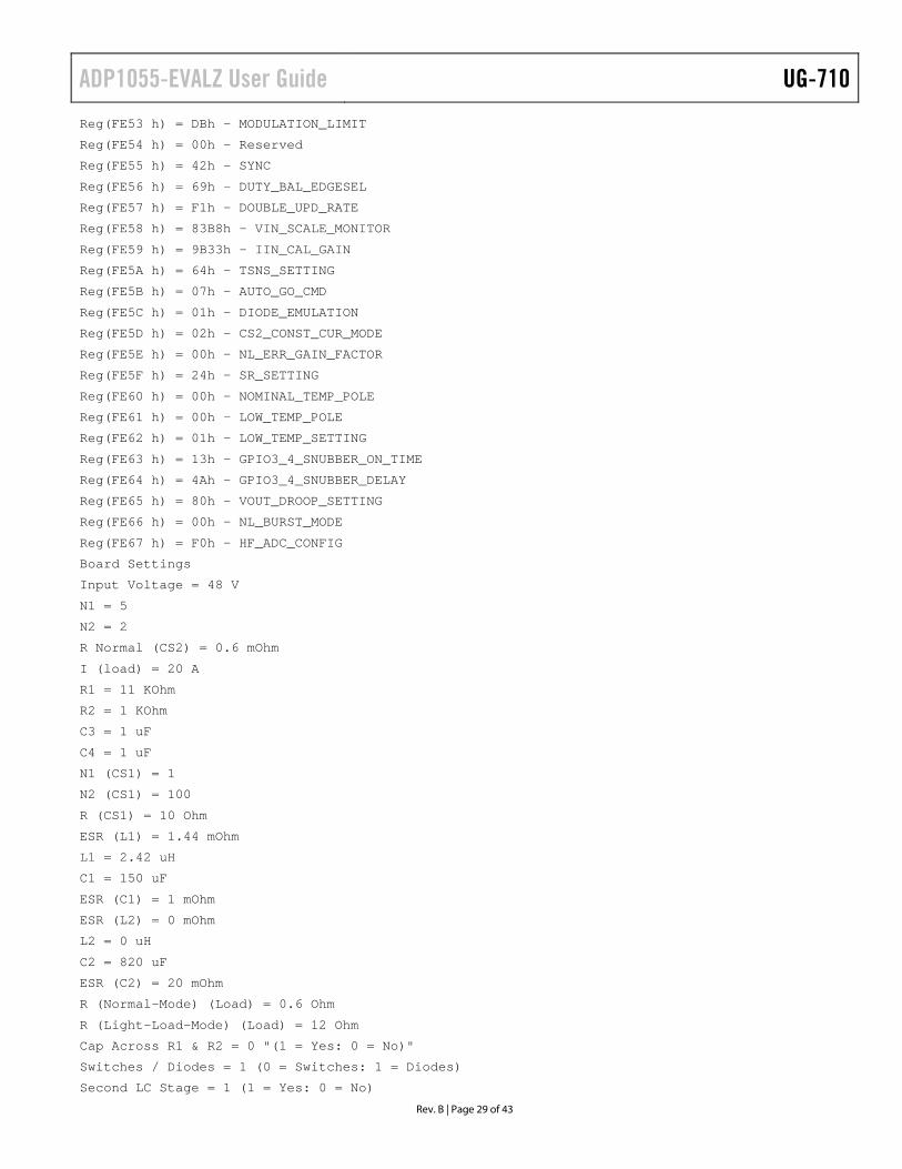
GUI 55S SETTINGS FILE Copy the contents below into a text file and rename it with using an extension of .55s. Load this file in the GUI using the Load settings from file option. Ensure that the last line of the .55s file does not have a carriage return. Reg(1 h) = 80h - OPERATION
Reg(2 h) = 1Fh - ON_OFF_CONFIG
Reg(10 h) = 00h - WRITE_PROTECT
Reg(1B h) = 00780079007A007B007D007E007C0080h - SMBALERT_MASK
Reg(20 h) = 15h - VOUT_MODE
Reg(21 h) = 6000h - VOUT_COMMAND
Reg(22 h) = 0068h - VOUT_TRIM
Reg(23 h) = 0000h - VOUT_CAL_OFFSET
Reg(24 h) = 999Ah - VOUT_MAX
Reg(27 h) = 8000h - VOUT_TRANSITION_RATE
Reg(28 h) = 8000h - VOUT_DROOP
Reg(29 h) = 9AA7h - VOUT_SCALE_LOOP
Reg(2A h) = 9AA6h - VOUT_SCALE_MONITOR
Reg(33 h) = EBE8h - FREQUENCY_SWITCH
Reg(35 h) = E800h - VIN_ON
Reg(36 h) = E800h - VIN_OFF
Reg(37 h) = 0000h - INTERLEAVE
Reg(38 h) = B266h - IOUT_CAL_GAIN
Reg(39 h) = 8000h - IOUT_CAL_OFFSET
Reg(40 h) = 6C00h - VOUT_OV_FAULT_LIMIT
Reg(41 h) = FCh - VOUT_OV_FAULT_RESPONSE
Reg(42 h) = 6800h - VOUT_OV_WARN_LIMIT
Reg(43 h) = 4A65h - VOUT_UV_WARN_LIMIT
Reg(44 h) = 4800h - VOUT_UV_FAULT_LIMIT
Reg(45 h) = 3Ah - VOUT_UV_FAULT_RESPONSE
Reg(46 h) = E991h - IOUT_OC_FAULT_LIMIT
Reg(47 h) = FCh - IOUT_OC_FAULT_RESPONSE
Reg(48 h) = 0000h - IOUT_OC_LV_FAULT_LIMIT
Reg(49 h) = 00h - IOUT_OC_LV_FAULT_RESPONSE
Reg(4A h) = E971h - IOUT_OC_WARN_LIMIT
Reg(4B h) = E800h - IOUT_UC_FAULT_LIMIT
Reg(4C h) = B8h - IOUT_UC_FAULT_RESPONSE
Reg(4F h) = F1B8h - OT_FAULT_LIMIT
Reg(50 h) = FFh - OT_FAULT_RESPONSE
Reg(51 h) = F17Dh - OT_WARN_LIMIT
Reg(55 h) = EA1Ch - VIN_OV_FAULT_LIMIT
Reg(56 h) = 3Ch - VIN_OV_FAULT_RESPONSE
Reg(59 h) = E908h - VIN_UV_FAULT_LIMIT
Reg(5A h) = 3Ah - VIN_UV_FAULT_RESPONSE
Reg(5B h) = D1E0h - IIN_OC_FAULT_LIMIT
Reg(5C h) = FCh - IIN_OC_FAULT_RESPONSE
Reg(5E h) = 0000h - POWER_GOOD_ON
Reg(5F h) = 0000h - POWER_GOOD_OFF
Rev. B | Page 26 of 43
ADP1055-EVALZ User Guide UG-710 Reg(60 h) = 0000h - TON_DELAY
Reg(61 h) = 0028h - TON_RISE
Reg(62 h) = 0032h - TON_MAX_FAULT_LIMIT
Reg(63 h) = 38h - TON_MAX_FAULT_RESPONSE
Reg(64 h) = 0000h - TOFF_DELAY
Reg(65 h) = 000Ah - TOFF_FALL
Reg(66 h) = 0032h - TOFF_MAX_WARN_LIMIT
Reg(68 h) = 012Ch - POUT_OP_FAULT_LIMIT
Reg(69 h) = 81h - POUT_OP_FAULT_RESPONSE
Reg(D0 h) = 4Bh - SLV_ADDR_SELECT
Reg(F4 h) = 003E000000FF0000FFFF60007F70FB01FF00037FDE639FFF03E8079F0A65000E20h - CMD_MASK
Reg(F5 h) = FFFFFFFFFF000000FFFFFFFFFFFFFFFFFFFFFFFFFF15h - EXTCMD_MASK
Reg(FE01 h) = 10h - NM_DIGFILT_LF_GAIN_SETTING
Reg(FE02 h) = E1h - NM_DIGFILT_ZERO_SETTING
Reg(FE03 h) = A4h - NM_DIGFILT_POLE_SETTING
Reg(FE04 h) = 16h - NM_DIGFILT_HF_GAIN_SETTING
Reg(FE05 h) = 31h - LLM_DIGFILT_LF_GAIN_SETTING
Reg(FE06 h) = F2h - LLM_DIGFILT_ZERO_SETTING
Reg(FE07 h) = E3h - LLM_DIGFILT_POLE_SETTING
Reg(FE08 h) = 3Ah - LLM_DIGFILT_HF_GAIN_SETTING
Reg(FE09 h) = 0Ch - SS_DIGFILT_LF_GAIN_SETTING
Reg(FE0A h) = AEh - SS_DIGFILT_ZERO_SETTING
Reg(FE0B h) = 00h - SS_DIGFILT_POLE_SETTING
Reg(FE0C h) = 1Eh - SS_DIGFILT_HF_GAIN_SETTING
Reg(FE0D h) = 33A1h - OUTA_REDGE_SETTING
Reg(FE0E h) = 33B8h - OUTA_FEDGE_SETTING
Reg(FE0F h) = 0210h - OUTB_REDGE_SETTING
Reg(FE10 h) = 0228h - OUTB_FEDGE_SETTING
Reg(FE11 h) = 0210h - OUTC_REDGE_SETTING
Reg(FE12 h) = 0228h - OUTC_FEDGE_SETTING
Reg(FE13 h) = 33A1h - OUTD_REDGE_SETTING
Reg(FE14 h) = 33B8h - OUTD_FEDGE_SETTING
Reg(FE15 h) = 0348h - SR1_REDGE_SETTING
Reg(FE16 h) = 00A0h - SR1_FEDGE_SETTING
Reg(FE17 h) = 34D8h - SR2_REDGE_SETTING
Reg(FE18 h) = 3230h - SR2_FEDGE_SETTING
Reg(FE19 h) = 33A0h - SR1_REDGE_LLM_SETTING
Reg(FE1A h) = 33B8h - SR1_FEDGE_LLM_SETTING
Reg(FE1B h) = 0210h - SR2_REDGE_LLM_SETTING
Reg(FE1C h) = 0228h - SR2_FEDGE_LLM_SETTING
Reg(FE1D h) = 00h - ADT_CONFIG
Reg(FE1E h) = 00h - ADT_THRESHOLD
Reg(FE1F h) = 88h - OUTA_DEAD_TIME
Reg(FE20 h) = 88h - OUTB_DEAD_TIME
Reg(FE21 h) = 88h - OUTC_DEAD_TIME
Reg(FE22 h) = 88h - OUTD_DEAD_TIME
Reg(FE23 h) = 88h - SR1_DEAD_TIME
Rev. B | Page 27 of 43
UG-710 ADP1055-EVALZ User Guide Reg(FE24 h) = 88h - SR2_DEAD_TIME
Reg(FE25 h) = C0h - VSBAL_SETTING
Reg(FE26 h) = 23h - VSBAL_OUTA_B
Reg(FE27 h) = 32h - VSBAL_OUTC_D
Reg(FE28 h) = C8h - VSBAL_SR1_2
Reg(FE29 h) = 04h - FFWD_SETTING
Reg(FE2A h) = 12h - ISHARE_SETTING
Reg(FE2B h) = 00h - ISHARE_BANDWIDTH
Reg(FE2C h) = 01h - IIN_OC_FAST_SETTING
Reg(FE2D h) = FFh - IOUT_OC_FAST_SETTING
Reg(FE2E h) = 02h - IOUT_UC_FAST_SETTING
Reg(FE2F h) = A9h - VOUT_OV_FAST_SETTING
Reg(FE30 h) = 69B5h - DEBOUNCE_SETTING_1
Reg(FE31 h) = 020Fh - DEBOUNCE_SETTING_2
Reg(FE32 h) = 0A05h - DEBOUNCE_SETTING_3
Reg(FE33 h) = 0000h - DEBOUNCE_SETTING_4
Reg(FE34 h) = 84h - VOUT_OV_FAST_FAULT_RESPONSE
Reg(FE35 h) = 80h - IOUT_OC_FAST_FAULT_RESPONSE
Reg(FE36 h) = B8h - IOUT_UC_FAST_FAULT_RESPONSE
Reg(FE37 h) = FCh - IIN_OC_FAST_FAULT_RESPONSE
Reg(FE38 h) = B8h - ISHARE_FAULT_RESPONSE
Reg(FE39 h) = 3Fh - GPIO1_FAULT_RESPONSE
Reg(FE3A h) = 38h - GPIO2_FAULT_RESPONSE
Reg(FE3B h) = 3Fh - GPIO3_FAULT_RESPONSE
Reg(FE3C h) = 38h - GPIO4_FAULT_RESPONSE
Reg(FE3D h) = C0h - PWM_FAULT_MASK
Reg(FE3E h) = 55h - DELAY_TIME_UNIT
Reg(FE3F h) = 00h - WDT_SETTING
Reg(FE40 h) = 35h - GPIO_SETTING
Reg(FE41 h) = 5Ch - GPIO1_2_KARNAUGH_MAP
Reg(FE42 h) = 06h - GPIO3_4_KARNAUGH_MAP
Reg(FE43 h) = 00h - PGOOD_FAULT_DEB
Reg(FE44 h) = 0009h - PGOOD1_FAULT_SELECT
Reg(FE45 h) = 0080h - PGOOD2_FAULT_SELECT
Reg(FE46 h) = 0000h - SOFT_START_BLANKING
Reg(FE47 h) = 0000h - SOFT_STOP_BLANKING
Reg(FE48 h) = 00h - BLACKBOX_SETTING
Reg(FE49 h) = 00h - PWM_DISABLE_SETTING
Reg(FE4A h) = 88h - FILTER_TRANSITION
Reg(FE4B h) = 39h - DEEP_LLM_SETTING
Reg(FE4C h) = 87h - DEEP_LLM_DISABLE_SETTING
Reg(FE4D h) = 44h - OVP_FAULT_CONFIG
Reg(FE4E h) = 21h - CS1_SETTING
Reg(FE4F h) = E5h - CS2_SETTING
Reg(FE50 h) = DEh - PULSE_SKIP_AND_SHUTDOWN
Reg(FE51 h) = 03h - SOFT_START_SETTING
Reg(FE52 h) = 00h - SR_DELAY
Rev. B | Page 28 of 43
ADP1055-EVALZ User Guide UG-710 Reg(FE53 h) = DBh - MODULATION_LIMIT
Reg(FE54 h) = 00h - Reserved
Reg(FE55 h) = 42h - SYNC
Reg(FE56 h) = 69h - DUTY_BAL_EDGESEL
Reg(FE57 h) = F1h - DOUBLE_UPD_RATE
Reg(FE58 h) = 83B8h - VIN_SCALE_MONITOR
Reg(FE59 h) = 9B33h - IIN_CAL_GAIN
Reg(FE5A h) = 64h - TSNS_SETTING
Reg(FE5B h) = 07h - AUTO_GO_CMD
Reg(FE5C h) = 01h - DIODE_EMULATION
Reg(FE5D h) = 02h - CS2_CONST_CUR_MODE
Reg(FE5E h) = 00h - NL_ERR_GAIN_FACTOR
Reg(FE5F h) = 24h - SR_SETTING
Reg(FE60 h) = 00h - NOMINAL_TEMP_POLE
Reg(FE61 h) = 00h - LOW_TEMP_POLE
Reg(FE62 h) = 01h - LOW_TEMP_SETTING
Reg(FE63 h) = 13h - GPIO3_4_SNUBBER_ON_TIME
Reg(FE64 h) = 4Ah - GPIO3_4_SNUBBER_DELAY
Reg(FE65 h) = 80h - VOUT_DROOP_SETTING
Reg(FE66 h) = 00h - NL_BURST_MODE
Reg(FE67 h) = F0h - HF_ADC_CONFIG
Board Settings
Input Voltage = 48 V
N1 = 5
N2 = 2
R Normal (CS2) = 0.6 mOhm
I (load) = 20 A
R1 = 11 KOhm
R2 = 1 KOhm
C3 = 1 uF
C4 = 1 uF
N1 (CS1) = 1
N2 (CS1) = 100
R (CS1) = 10 Ohm
ESR (L1) = 1.44 mOhm
L1 = 2.42 uH
C1 = 150 uF
ESR (C1) = 1 mOhm
ESR (L2) = 0 mOhm
L2 = 0 uH
C2 = 820 uF
ESR (C2) = 20 mOhm
R (Normal-Mode) (Load) = 0.6 Ohm
R (Light-Load-Mode) (Load) = 12 Ohm
Cap Across R1 & R2 = 0 "(1 = Yes: 0 = No)"
Switches / Diodes = 1 (0 = Switches: 1 = Diodes)
Second LC Stage = 1 (1 = Yes: 0 = No)
Rev. B | Page 29 of 43
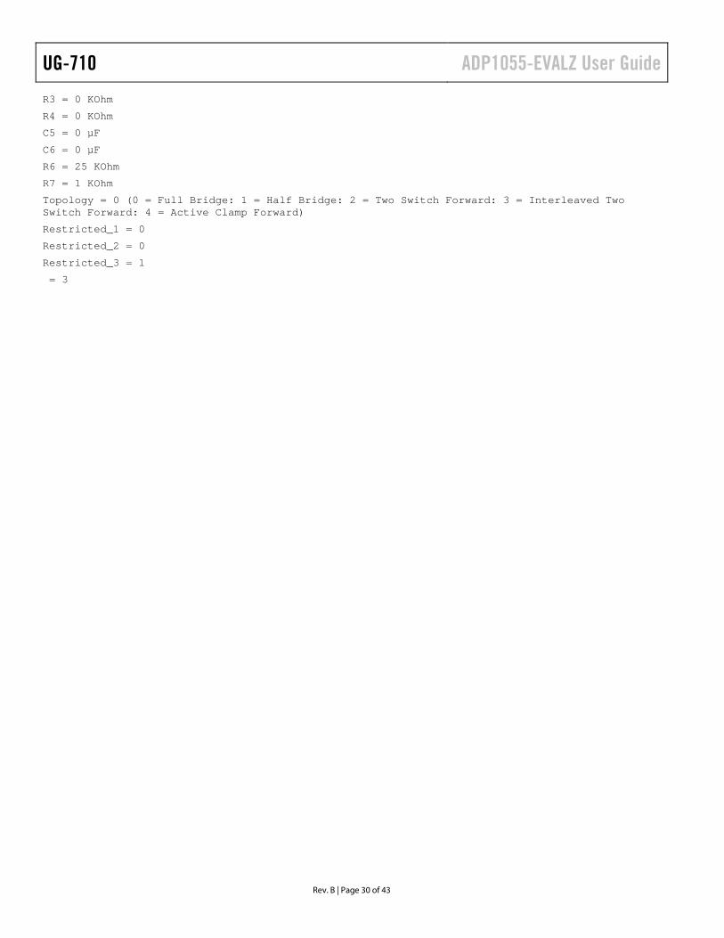
UG-710 ADP1055-EVALZ User Guide R3 = 0 KOhm
R4 = 0 KOhm
C5 = 0 µF
C6 = 0 µF
R6 = 25 KOhm
R7 = 1 KOhm
Topology = 0 (0 = Full Bridge: 1 = Half Bridge: 2 = Two Switch Forward: 3 = Interleaved Two Switch Forward: 4 = Active Clamp Forward)
Restricted_1 = 0
Restricted_2 = 0
Restricted_3 = 1
= 3
Rev. B | Page 30 of 43
ADP1055-EVALZ User Guide UG-710
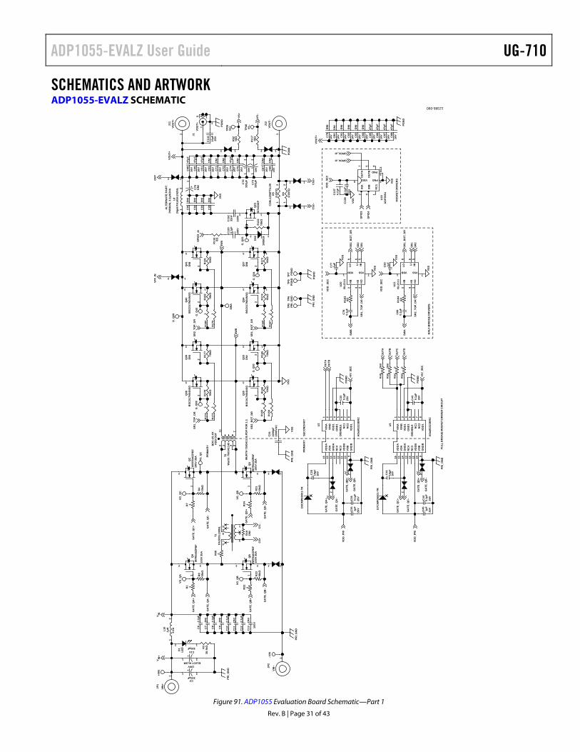
SCHEMATICS AND ARTWORK ADP1055-EVALZ SCHEMATIC
PRIM
AR
Y BD
C-2
5-XX
AD
D D
OT
CSN
L120
6FT1
L00
FULL
BR
IDG
E M
OSF
ET D
RIV
ER C
IRC
UIT
PRIM
AR
Y
SEC
ON
DA
RY
ALT
ERN
ATE
PA
RT:
100V
25V
16V
16V
25V
25V
25V
25V
16V
16V
16V
16V
16V
16V
16V
16V
16V
16V
16V
16V
VOU
T+
100V
MO
SFET
DR
IVER
S
2000
VAC
HA
LF-B
RID
GE
DR
IVER
S
25V
PGN
D
PG
ND
PRI_
GN
D
VS–
VS+
25V
100V
25V
P059
6NL
3.2µ
H/2
4A
ELECT ALUM100V
9.2A
100V
35A
100V
35A
100V
35A
100V
35A
16V
16V
16V
16V
16V
16V
16V
16V
16V
16V
PGN
DPR
I_G
ND
PRI_
GN
D
PRI_
GN
D
PGN
D
PGN
DVS
S
VSS
VSS
PRI_
GN
DVS
S
VSS
VSS
VSS
VSS
PRI_
GN
D
PGN
D
PGN
D
PRI_
GN
D
VSS
PGN
D
GA
TE_Q
A–
GA
TE_Q
C-
GA
TE_Q
C+
CS+
GA
TE_Q
A+
GA
TE_Q
B+
GA
TE_Q
D–
V IN+
CS–
VDD
_PR
IG
ATE
_QD
+
GA
TE_Q
D–
OU
TC
OU
TD
OU
TAO
UTB
+5V_
SEC
+5V_
SEC
GA
TE_Q
A–
VDD
_PR
IG
ATE
_QB
+
GA
TE_Q
B-
OU
TA
OU
TB
GA
TE_Q
D+
GA
TE_Q
C+
GA
TE_Q
C-
GA
TE_Q
A+
OVP
VS+
VS–
SR1_
TOP_
DR
SR2_
BO
T_D
RSR
1_B
OT_
DR
SR2_
TOP_
DR
GPI
O3_
dr
VFF_
IN
GPIO3_dr
GPIO4_dr
GPI
O3
GPI
O4
VDD
_SEC
SWB
SR1_
TOP_
DR
SR2_
BO
T_D
R
SR2
SR1
VDD
_SEC
SWA
SR2_
TOP_
DR
SR1_
BO
T_D
R
SR1
SR2
VDD
_SEC
GA
TE_Q
B–
SWA
SWB
CS2
–C
S2+
VOU
T+
V IN
VOU
T+
C7
D
NI
Q40
BSC
017N
04N
SG
3
2
1
R17
51
G_Q
40
+
C2330µF
1 2
C87
4
7µF
R8
10kΩ
C85
4
7µF
R15
91
G_Q
30
JP2
VIN
–
1
R11
710
Ω
C13
D
NI
TP5
12
TP46
C91
D
NI
C77 1µF
+VIN
Q39 DN
I
3
2
1
C83
D
NI
C36
0.1µ
F
Q33
DN
I
3
2
1
D7C
MPD
5001
-TR
12
C95
D
NI
C67
D
NI
R17
3
10kΩ
C82
D
NI
R18
30Ω
–VIN
C43 0.1µ
F
12
R1 2
J12
VOU
T–
1
C72
D
NI
C14
110
µF C79
D
NI
C74
4
7µF
C68
D
NI
U5
AD
uM32
23B
RZ
VIN
A1
VIN
B2
VDD
13
GN
D1
4
DIS
AB
LE5
NC
16
NC
27
VDD
18
GN
DB
9VO
B10
VDD
B11
NC
312
NC
413
GN
DA
14VO
A15
VDD
A16
C13
8
0.1
µF
VG_Q
B
R16
71
R18
2
10kΩ
C12
2
.2µF
R18
01
QD
IRFR
540Z
PBF
2
1
3
Q41
DN
I
3
2
1
L824
µH P
A14
94.2
42N
L1
2
Q23
SI74
63D
P
1
2
3
C6
2
.2µF
C51
4
7µF
C41
10µF
R31
10kΩ
C35 1µ
F
R16
81
U19
AD
P365
4
NC
11
INA
2
PND 3
INB
4O
UTB
5
VDD6
OU
TA7
NC
28
PND9
12
VG_Q
D
C12
00.
1µF
L10
1µH
12
R68 0
QB
IRFR
540Z
PBF
2
1
3
U2
AD
uM32
23B
RZ
VIN
A1
VIN
B2
VDD
13
GN
D1
4
DIS
AB
LE5
NC
16
NC
27
VDD
18
GN
DB
9VO
B10
VDD
B11
NC
312
NC
413
GN
DA
14VO
A15
VDD
A16
C28
10µF
R53
0
U20
ISL2
111
VDD1
HB
2
HO
3H
S4
LO8
VSS7
LI6
HI
5
+
C73
330µ
F1
2
R49
DN
I
R18
40Ω
R19
DN
I
D1
LED
2 1
C88
4
7µF
R4
10kΩ
G_Q
23
C86
4
7µF
12
VG_Q
C
C13
74.
7µF
R22 2
TP7
TP6
C11
D
NI
J1
1
2
345
C19
233
nF
R17
7
10kΩ
12
C84
D
NI
T2W
urth
: 750
3411
45211 7
3 4 5
C53
D
NI
C49
4
7µF
U21
ISL2
111
VDD1
HB
2
HO
3H
S4
LO8
VSS7
LI6
HI
5
D5C
MPD
5001
-TR
C89
0.1µ
F
JP1
VIN
+
1
C81
D
NI
SWA
12
VG_Q
A
C71
D
NI
C24
2200
pF
12
C8
2
.2µF
C93
D
NI
R50
DN
I
Q37
DN
I
3
2
1
C80
D
NI
12
R16
5
10kΩ
R11
60Ω
R24 2
12
R52
10Ω
TP9
Q38
BSC
017N
04N
SG
3
2
1
QC
IRFR
540Z
PBF
2
1
3
C90 1µ
F
Q34
BSC
017N
04N
SG
3
2
1
C10
2
.2µF
TP26
C75
D
NI
C45 1µ
F
R16
01
R12
210
kΩ
C33 0.1µ
F
C44
0.1µ
F
D_Q
39
R7 2
J11
VOU
T+
1
R17
8
10kΩ
G_Q
38
Q30
BSC
017N
04N
SG
3
2
1
R18
1
10kΩ
+
C76
DN
I
12
R17
4
10kΩ
C9
D
NI
R9
0.00
1Ω1
2
1N58
19D62
2 1
12
R54
0
R3
30.1
kΩ
T1PA
1005
.100
NL
7 3
8
1
2
4
65
+
C70
330µ
F1
2
12
C92
D
NI
R17
91
VS_Q
C
G_Q
34
+
C14330µF
1 2
C78
0.1µ
F
R16
6
10kΩ
QA
IRFR
540Z
PBF
2
1
3
R5
0.00
1Ω1
2
R17
61
R23
10kΩ
C48
4
7µF
WU
RTH
750
3411
36.P
DF
FOR
1:1
12386-090
Figure 91. ADP1055 Evaluation Board Schematic—Part 1
Rev. B | Page 31 of 43
UG-710 ADP1055-EVALZ User Guide
CO
M1
AD
P105
5 D
AU
GH
TER
CA
RD
CO
NN
ECTI
ON
S
I2C
INTE
RFA
CE
AN
D F
ILTE
RIN
G
MIR
O M
ATC
H
CO
M2
PRIM
AR
Y +9
VSE
CO
ND
AR
Y +9
V
AU
XILL
AR
U P
SU
LIN
E FE
ED-F
OR
WA
RD
CS1
SEN
SIN
G
RED
iSH
AR
E
CS1
VDD
_SEC
IR
P_
DD
V
RED
AG
ND
AG
ND
AG
ND
AG
ND
AG
ND
AG
ND
AG
ND
AG
ND
PGN
D
PRI_
GN
D
PRI_
GN
D
PGN
D
PGN
D
+5V
SDA
SCL
+5V_
SEC
VS+
SMB
ALR
T
OVP
GPI
O1
GPI
O2
SCL
SYN
C
SDA
SHA
REi
SR2
SR1
VS–
CS1
OU
TA
OU
TB
OU
TC
OU
TD
VDD
_SEC
Vin
GPI
O4
GPI
O3
+5V_
SEC
VDD
_PR
I
CS2
+
CS2
–
VFF_
IN
VFF
VFF
CS+
CS–
CS1
VDD
_SEC
VDD
_PR
I
SPA
RE
+5V_
SEC
VDD
_SEC
+5V_
SEC
C55 DN
I
R15
34.
75kΩ
12
C59
33pF
D8
2 1
TP11
SW2
PSO
N
C56
33pF
C60
1nF
TP55
R11
10kΩ
R76
19.1
kΩ
R15
110
Ω
1N58
19
D16
21
J7
SCL
1
GN
D A
2
SDA
3
VBU
S4
SPI M
ISO
5
NC
6
SPI S
CLK
7
SPI M
OSI
8
SPI C
S A
9
GN
D B
10
D75
MM
BD
7000
HS-
7-F
13
2
R15
210
Ω
J5
123456789101112131415161718192021222324252627282930
R77
10kΩ
R67
100Ω
TP54
R62
0
Ω
D6
2 1
C57
33pF
R65
100Ω
C54
DN
I
R59
0
C61
220p
F
R10
10kΩ
J6 5V1
SCL
2
SDA
3
GN
D4
D76
MM
BD
7000
HS-
7-F
13
2
C58
33pF
J4
VIN
_AU
X11
PRI_
GN
D1
2
VIN
_AU
X23
PRI_
GN
D2
4
VIN
_AU
X35
PRI_
GN
D3
6
VDD
_PR
I17
VDD
_PR
I28
NC
19
NC
210
SPA
RE
11
+5V_
SEC
12
+9V_
SEC
113
PGN
D1
14+9
V_SE
D2
15
PGN
D2
16
TP53
C18
910
00pF
R63
205Ω
Q12
BC847A,215
TEM
PER
ATU
RE
–
AN
ALO
G S
HA
RE
BU
S FE
EDB
AC
K P
IN
I2C
SER
IAL
DA
TA IN
PUT
AN
D O
UTP
UT
I2C
SER
IAL
CLO
CK
INPU
T
TEM
PER
ATU
RE
+
SYN
CH
RO
NIZ
ATI
ON
GEN
ERA
L PU
RPO
SE IN
PUT/
OU
TPU
T
SMB
ALE
RT
POW
ER S
UPP
LY O
N IN
PUT
GEN
ERA
L PU
RPO
SE IN
PUT/
OU
TPU
T
PWM
OU
TPU
T FO
R P
RIM
AR
Y SI
DE
SWIT
CH
PWM
OU
TPU
T FO
R P
RIM
AR
Y SI
DE
SWIT
CH
PWM
OU
TPU
T FO
R P
RIM
AR
Y SI
DE
SWIT
CH
PWM
OU
TPU
T FO
R P
RIM
AR
Y SI
DE
SWIT
CH
PRIM
AR
Y SI
DE
CU
RR
ENT
SEN
SE IN
PUT
VOLT
AG
E FE
ED F
OR
WA
RD
SYN
CH
RO
NO
US
REC
TIFI
ER O
UTP
UT
1
SYN
CH
RO
NO
US
REC
TIFI
ER O
UTP
UT
2
INVE
RTI
NG
DIF
FER
ENTI
AL
CU
RR
ENT
SEN
SE IN
PUT
NO
N-IN
VER
TIN
G D
IFFE
REN
TIA
L C
UR
REN
T SE
NSE
INPU
T
AG
ND
OVE
RVO
LTA
GE
PRO
TEC
TIO
N
GPI
O3
NO
N-IN
VER
TIN
G R
EMO
TE V
OLT
AG
E SE
NSE
INPU
T
INVE
RTI
NG
REM
OTE
VO
LTA
GE
SEN
SE IN
PUT
5V O
R G
PIO
3
3.3V
OR
GPI
O4
AN
ALO
G G
ND
12386-091
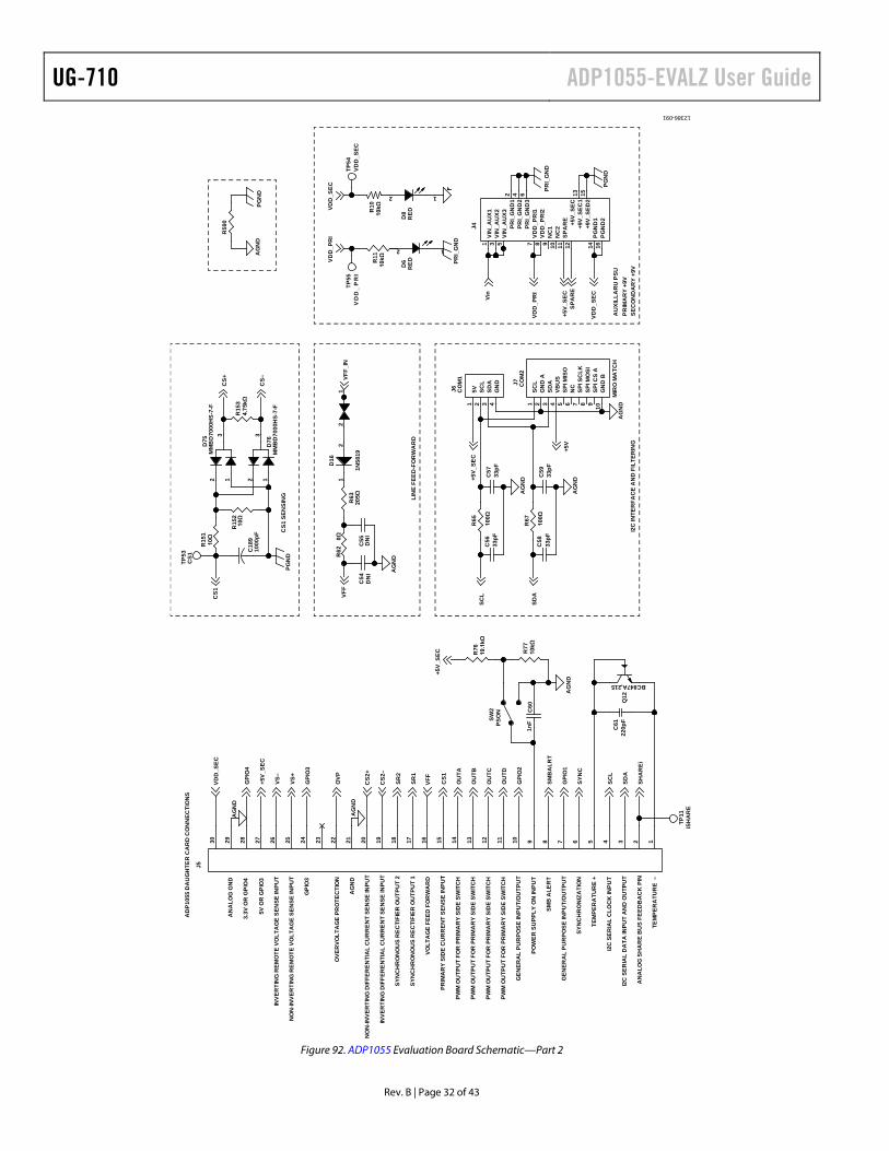
Figure 92. ADP1055 Evaluation Board Schematic—Part 2
Rev. B | Page 32 of 43
ADP1055-EVALZ User Guide UG-710
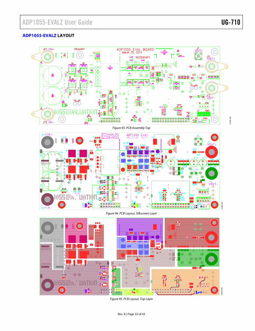
ADP1055-EVALZ LAYOUT
1238
6-09
2
Figure 93. PCB Assembly Top
1238
6-09
3
Figure 94. PCB Layout, Silkscreen Layer
1238
6-09
4
Figure 95. PCB Layout, Top Layer
Rev. B | Page 33 of 43
UG-710 ADP1055-EVALZ User Guide
1238
6-09
5
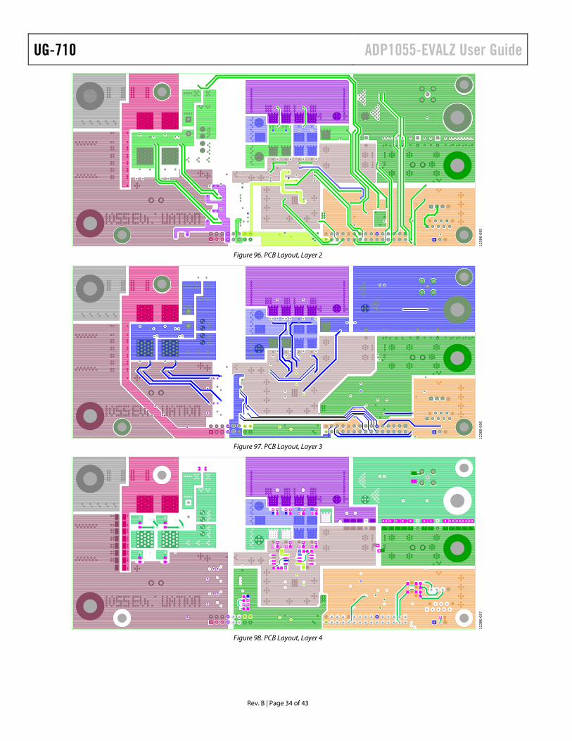
Figure 96. PCB Layout, Layer 2
1238
6-09
6
Figure 97. PCB Layout, Layer 3
1238
6-09
7
Figure 98. PCB Layout, Layer 4
Rev. B | Page 34 of 43

ADP1055-EVALZ User Guide UG-710
1238
6-09
8
Figure 99. PCB Layout, Bottom Layout
1238
6-09
9
Figure 100. PCB Assembly Bottom
Rev. B | Page 35 of 43

UG-710 ADP1055-EVALZ User Guide
ADP1055DC1-EVALZ SCHEMATIC
100V
RED
GREEN
DN
I
CO
M1
CO
M2
WH
ITE
V SEN
SE IS
DED
ICA
TED
TR
AC
ETO
VD
D P
IN O
F A
DP1
055
CO
NN
ECT
GR
OU
ND
TO
EXP
OSE
D P
AD
OF
LFC
SPA
ND
MA
KE
THE
CO
PPER
GR
OU
ND
PLA
NE
RES
RES
ISTO
R C
LOSE
TO
IC
AN
D A
GN
DVD
D A
ND
VC
OR
E SH
OU
LD B
E C
LOSE
TO
AG
ND
11kΩ
, 1kΩ
DIV
IDER
PO
INT
SHO
ULD
BE
CLO
SE T
O T
HE
VS+
PISA
ME
FOR
OVP
DIV
IDER
SAM
E FO
R V
FF D
IVID
ERC
13 A
ND
R25
CLO
SE T
O IC
CO
NTR
OL
PIN
CA
P SH
OU
LD B
E C
LOSE
TO
CTR
L PI
N
+3.3
V
+12V
+5V
+3.3
V
+3.3
V
+5V
+3.3
V
+3.3
V
+5V
+3.3
V
+3.3
V
+5V
+12V
SHA
REi
SMB
ALR
T CTR
L
GPI
O1
SYNC
OUTD
OUTC
OUTB
OUTA
SR2
SR1
VFF
VS–
VS+
GPI
O3
OVP
SR2
SR1
VFF
CS1
OU
TA
OU
TB
OU
TC
OU
TD
CTR
L
SMB
ALR
T
SCL_
PF
SDA
_PF
SHA
REi
SCL
SDA
GPI
O2
JTD
JRTN
VS+
GPI
O3
GPIO4
GPI
O1
GPI
O2
SYN
C
GPI
O3
GPI
O4
CS1
OVP
CS2
+
CS2
_HS+
CS2
_HS+
CS2
–
CS2
+
CS2
–
SCL
SDA
SCL_
PF
SDA
_PF
SDA
SCL
VS–
JTD
V SEN
SE
V SEN
SE
JRTN
D9
LED
12
R18
0
R4
0
R15
D
NI
Q2
DN
I
1
32
C20
33pF
C6
0.1µ
F
C25
DN
I
R47
100
R66
DN
I
R2
0
R11 1kΩ
C17
0.1µ
F
C5
DN
I
C4
DN
I
R24
1kΩ
R67
SHO
RTP
IN
12
C10
1000
pFR
250
C9
1000
pF
Q1
DN
I1
3 2
R30
2.2k
Ω
R62
2.
2kΩ
R64 0Ω
R14 1k
Ω
R8 10kΩ
D51N4148
2 1
R31
2.2k
Ω
C2 0.1µF
U3
AD
8218
BR
MZ
1+I
N
2 VS
3ENB
4GND
5O
UT
6N
C
7REF
8–I
N
R9
11kΩ
C1 0.33µF
R12 1kΩ
R6 1Ω0k
C21
33pF
R63
2.
2kΩ
R10 2.2kΩ
R1
D
NI
J1
123456789101112131415161718192021222324252627282930
TEM
PER
ATU
RE
–
AN
ALO
G S
HA
RE
BU
S FE
EDB
AC
K P
IN
I2C
SER
IAL
DA
TA IN
PUT
AN
D O
UTP
UT
I2C
SER
IAL
CLO
CK
INPU
T
TEM
PER
ATU
RE
+
SYN
CH
RO
NIZ
ATI
ON
GEN
ERA
L PU
RPO
SE IN
PUT/
OU
TPU
T
SMB
ALE
RT
POW
ER S
UPP
LY O
N IN
PUT
GEN
ERA
L PU
RPO
SE IN
PUT/
OU
TPU
T
PWM
OU
TPU
T FO
R P
RIM
AR
Y SI
DE
SWIT
CH
PWM
OU
TPU
T FO
R P
RIM
AR
Y SI
DE
SWIT
CH
PWM
OU
TPU
T FO
R P
RIM
AR
Y SI
DE
SWIT
CH
PWM
OU
TPU
T FO
R P
RIM
AR
Y SI
DE
SWIT
CH
PRIM
AR
Y SI
DE
CU
RR
ENT
SEN
SE IN
PUT
VOLT
AG
E FE
ED F
OR
WA
RD
SYN
CH
RO
NO
US
REC
TIFI
ER O
UTP
UT
1
SYN
CH
RO
NO
US
REC
TIFI
ER O
UTP
UT
2
INVE
RTI
NG
DIF
FER
ENTI
AL
CU
RR
ENT
SEN
SE IN
PUT
NO
N-IN
VER
TIN
G D
IFFE
REN
TIA
L C
UR
REN
T SE
NSE
INPU
T
AG
ND
OVE
RVO
LTA
GE
PRO
TEC
TIO
N
N/C
GPI
O3
NO
N-IN
VER
TIN
G R
EMO
TE V
OLT
AG
E SE
NSE
INPU
T
INVE
RTI
NG
REM
OTE
VO
LTA
GE
SEN
SE IN
PUT
5V O
R G
PIO
3
3.3V
OR
GPI
O4
AN
ALO
G G
ND
C23
1
µF
R19
DN
I
R28
DN
I
R46 100
R16
0
C16
4.7
µF
J3
SCL
1
GN
D A
2
SDA
3
VBU
S4
SPI M
ISO
5
NC
6
SPI S
CLK
7
SPI M
OSI
8
SPI C
S A
9
GN
D B
10
C3
DN
I
R29
2.2k
Ω
D19
1N41
48
21
D4
1N41
48
2 1
U1
AD
P105
5
OVP
1
VS+
2
VS–
3
CS2
+4
CS2
–5
NC
6
VFF
7
CS1
8
SR19
SR210
OUTA11
OUTB12
SYNC15
OUTC13
OUTD14
GPIO416
GPI
O3
17G
PIO
218
GPI
O1
19
CTR
L20
SCL
21
SDA
22SM
BA
LRT#
23SH
AR
Ei24
VCORE25
VDD26
DGND27
AGND28
JRTN29
RES30
ADD31
JTD32
PAD33
D21
1N41
48
21
R20
D
NI
R26
16.2
kΩ
U2
AD
P710
2AR
DZ-
3.3-
R7
1 VOU
T2
SEN
SE
3
GN
D1
4N
C
5EN
/UVL
O
6
GN
D2
7PG
8
VIN
C13
1000
pF
R27
1kΩ
R7
1kΩ
R5
11kΩ
C14
560p
F
C24 DN
I
R3
D
NI
D61N4148
2 1
D20
1N41
48
21
R65
1.5k
ΩD
221N
4148
21
C18
1
µF
C19 33pF
D7
1 2
R13 2.2kΩ
J2 VBU
S1
SCL
2
SDA
3
GN
D4
D8
1 2
C22
33pF
12386-100
Figure 101. ADP1055 Daughter Card Schematic
Rev. B | Page 36 of 43

ADP1055-EVALZ User Guide UG-710
ADP1055DC1-EVALZ LAYOUT
1238
6-10
1
Figure 102. PCB Assembly, Top
1238
6-10
2
Figure 103. PCB Layout, Silkscreen Layer Top
1238
6-10
3
Figure 104. PCB Layout, Top Layer
1238
6-10
4
Figure 105. PCB Layout, Layer 2
1238
6-10
5
Figure 106. PCB Layout, Layer 3
1238
6-10
6
Figure 107. PCB Layout, Bottom Layer
Rev. B | Page 37 of 43

UG-710 ADP1055-EVALZ User Guide
1238
6-10
7
Figure 108. PCB Layout, Silkscreen Bottom
1238
6-10
8
Figure 109. PCB Assembly, Bottom
Rev. B | Page 38 of 43
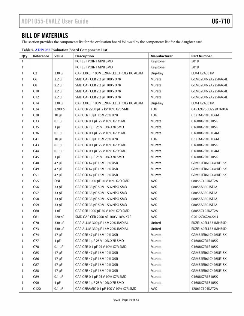
ADP1055-EVALZ User Guide UG-710
BILL OF MATERIALS The section provides the components list for the evaluation board followed by the components list for the daughter card.
Table 5. ADP1055 Evaluation Board Components List
Qty. Reference Value Description Manufacturer Part Number 1 PC TEST POINT MINI SMD Keystone 5019
1 PC TEST POINT MINI SMD Keystone 5019
1 C2 330 µF CAP 330 µF 100 V ±20% ELECTROLYTIC ALUM Digi-Key EEV-FK2A331M
1 C6 2.2 µF SMD CAP CER 2.2 µF 100 V X7R Murata GCM32DR72A225KA64L
1 C8 2.2 µF SMD CAP CER 2.2 µF 100 V X7R Murata GCM32DR72A225KA64L
1 C10 2.2 µF SMD CAP CER 2.2 µF 100 V X7R Murata GCM32DR72A225KA64L
1 C12 2.2 µF SMD CAP CER 2.2 µF 100 V X7R Murata GCM32DR72A225KA64L
1 C14 330 µF CAP 330 µF 100 V ±20% ELECTROLYTIC ALUM Digi-Key EEV-FK2A331M
1 C24 2200 pF CAP CER 2200 pF 2 kV 10% X7S SMD TDK C4532X7S3D222K160KA
1 C28 10 µF CAP CER 10 µF 16 V 20% X7R TDK C3216X7R1C106M
1 C33 0.1 µF CAP CER 0.1 µF 25 V 10% X7R SMD Murata C1608X7R1E105K
1 C35 1 µF CAP CER 1 µF 25 V 10% X7R SMD Murata C1608X7R1E105K
1 C36 0.1 µF CAP CER 0.1 µF 25 V 10% X7R SMD Murata C1608X7R1C104M
1 C41 10 µF CAP CER 10 µF 16 V 20% X7R TDK C3216X7R1C106M
1 C43 0.1 µF CAP CER 0.1 µF 25 V 10% X7R SMD Murata C1608X7R1E105K
1 C44 0.1 µF CAP CER 0.1 µF 25 V 10% X7R SMD Murata C1608X7R1C104M
1 C45 1 µF CAP CER 1 µF 25 V 10% X7R SMD Murata C1608X7R1E105K
1 C48 47 µF CAP CER 47 µF 16 V 10% X5R Murata GRM32ER61C476KE15K
1 C49 47 µF CAP CER 47 µF 16 V 10% X5R Murata GRM32ER61C476KE15K
1 C51 47 µF CAP CER 47 µF 16 V 10% X5R Murata GRM32ER61C476KE15K
1 C55 DNI CAP CER 1000 pF 50 V 10% X7R SMD AVX 08055C102KAT2A
1 C56 33 pF CAP CER 33 pF 50 V ±5% NPO SMD AVX 08055A330JAT2A
1 C57 33 pF CAP CER 33 pF 50 V ±5% NPO SMD AVX 08055A330JAT2A
1 C58 33 pF CAP CER 33 pF 50 V ±5% NPO SMD AVX 08055A330JAT2A
1 C59 33 pF CAP CER 33 pF 50 V ±5% NPO SMD AVX 08055A330JAT2A
1 C60 1 nF CAP CER 1000 pF 50 V 10% X7R SMD AVX 08055C102KAT2A
1 C61 220 pF SMD CAP CER 2200 pF 100 V 10% X7R AVX C2012C0G2A221J
1 C70 330 µF CAP ALUM 300 µF 16 V 20% RADIAL United EKZE160ELL331MHB5D
1 C73 330 µF CAP ALUM 330 µF 16 V 20% RADIAL United EKZE160ELL331MHB5D
1 C74 47 µF CAP CER 47 µF 16 V 10% X5R Murata GRM32ER61C476KE15K
1 C77 1 µF CAP CER 1 µF 25 V 10% X7R SMD Murata C1608X7R1E105K
1 C78 0.1 µF CAP CER 0.1 µF 25 V 10% X7R SMD Murata C1608X7R1E105K
1 C85 47 µF CAP CER 47 µF 16 V 10% X5R Murata GRM32ER61C476KE15K
1 C86 47 µF CAP CER 47 µF 16 V 10% X5R Murata GRM32ER61C476KE15K
1 C87 47 µF CAP CER 47 µF 16 V 10% X5R Murata GRM32ER61C476KE15K
1 C88 47 µF CAP CER 47 µF 16 V 10% X5R Murata GRM32ER61C476KE15K
1 C89 0.1 µF CAP CER 0.1 µF 25 V 10% X7R SMD Murata C1608X7R1E105K
1 C90 1 µF CAP CER 1 µF 25 V 10% X7R SMD Murata C1608X7R1E105K
1 C120 0.1 µF CAP CERAMIC 0.1 µF 100 V 10% X7R SMD AVX 12061C104KAT2A
Rev. B | Page 39 of 43
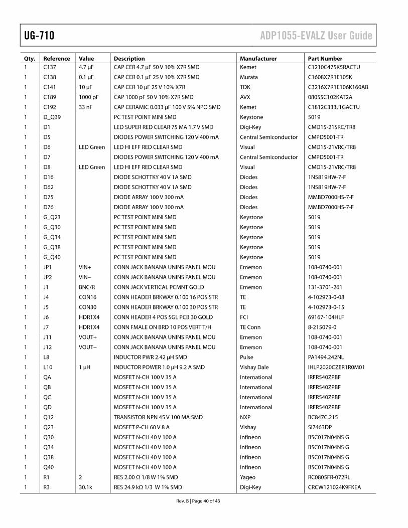
UG-710 ADP1055-EVALZ User Guide
Qty. Reference Value Description Manufacturer Part Number 1 C137 4.7 µF CAP CER 4.7 µF 50 V 10% X7R SMD Kemet C1210C475K5RACTU
1 C138 0.1 µF CAP CER 0.1 µF 25 V 10% X7R SMD Murata C1608X7R1E105K
1 C141 10 µF CAP CER 10 µF 25 V 10% X7R TDK C3216X7R1E106K160AB
1 C189 1000 pF CAP 1000 pF 50 V 10% X7R SMD AVX 08055C102KAT2A
1 C192 33 nF CAP CERAMIC 0.033 µF 100 V 5% NPO SMD Kemet C1812C333J1GACTU
1 D_Q39 PC TEST POINT MINI SMD Keystone 5019
1 D1 LED SUPER RED CLEAR 75 MA 1.7 V SMD Digi-Key CMD15-21SRC/TR8
1 D5 DIODES POWER SWITCHING 120 V 400 mA Central Semiconductor CMPD5001-TR
1 D6 LED Green LED HI EFF RED CLEAR SMD Visual CMD15-21VRC/TR8
1 D7 DIODES POWER SWITCHING 120 V 400 mA Central Semiconductor CMPD5001-TR
1 D8 LED Green LED HI EFF RED CLEAR SMD Visual CMD15-21VRC/TR8
1 D16 DIODE SCHOTTKY 40 V 1A SMD Diodes 1N5819HW-7-F
1 D62 DIODE SCHOTTKY 40 V 1A SMD Diodes 1N5819HW-7-F
1 D75 DIODE ARRAY 100 V 300 mA Diodes MMBD7000HS-7-F
1 D76 DIODE ARRAY 100 V 300 mA Diodes MMBD7000HS-7-F
1 G_Q23 PC TEST POINT MINI SMD Keystone 5019
1 G_Q30 PC TEST POINT MINI SMD Keystone 5019
1 G_Q34 PC TEST POINT MINI SMD Keystone 5019
1 G_Q38 PC TEST POINT MINI SMD Keystone 5019
1 G_Q40 PC TEST POINT MINI SMD Keystone 5019
1 JP1 VIN+ CONN JACK BANANA UNINS PANEL MOU Emerson 108-0740-001
1 JP2 VIN− CONN JACK BANANA UNINS PANEL MOU Emerson 108-0740-001
1 J1 BNC/R CONN JACK VERTICAL PCMNT GOLD Emerson 131-3701-261
1 J4 CON16 CONN HEADER BRKWAY 0.100 16 POS STR TE 4-102973-0-08
1 J5 CON30 CONN HEADER BRKWAY 0.100 30 POS STR TE 4-102973-0-15
1 J6 HDR1X4 CONN HEADER 4 POS SGL PCB 30 GOLD FCI 69167-104HLF
1 J7 HDR1X4 CONN FMALE ON BRD 10 POS VERT T/H TE Conn 8-215079-0
1 J11 VOUT+ CONN JACK BANANA UNINS PANEL MOU Emerson 108-0740-001
1 J12 VOUT− CONN JACK BANANA UNINS PANEL MOU Emerson 108-0740-001
1 L8 INDUCTOR PWR 2.42 µH SMD Pulse PA1494.242NL
1 L10 1 µH INDUCTOR POWER 1.0 µH 9.2 A SMD Vishay Dale IHLP2020CZER1R0M01
1 QA MOSFET N-CH 100 V 35 A International IRFR540ZPBF
1 QB MOSFET N-CH 100 V 35 A International IRFR540ZPBF
1 QC MOSFET N-CH 100 V 35 A International IRFR540ZPBF
1 QD MOSFET N-CH 100 V 35 A International IRFR540ZPBF
1 Q12 TRANSISTOR NPN 45 V 100 MA SMD NXP BC847C,215
1 Q23 MOSFET P-CH 60 V 8 A Vishay SI7463DP
1 Q30 MOSFET N-CH 40 V 100 A Infineon BSC017N04NS G
1 Q34 MOSFET N-CH 40 V 100 A Infineon BSC017N04NS G
1 Q38 MOSFET N-CH 40 V 100 A Infineon BSC017N04NS G
1 Q40 MOSFET N-CH 40 V 100 A Infineon BSC017N04NS G
1 R1 2 RES 2.00 Ω 1/8 W 1% SMD Yageo RC0805FR-072RL
1 R3 30.1k RES 24.9 kΩ 1/3 W 1% SMD Digi-Key CRCW121024K9FKEA
Rev. B | Page 40 of 43
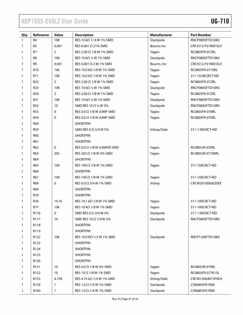
ADP1055-EVALZ User Guide UG-710
Qty. Reference Value Description Manufacturer Part Number 1 R4 10K RES 10 kΩ 1/ 4 W 1% SMD Stackpole RNCP0805FTD10K0
1 R5 0.001 RES 0.001 Ω 21% SMD Bourns Inc CRF2512-FV-R001ELF
1 R7 2 RES 2.00 Ω 1/8 W 1% SMD Yageo RC0805FR-072RL
1 R8 10K RES 10 kΩ ¼ W 1% SMD Stackpole RNCP0805FTD10K0
1 R9 0.001 RES 0.001 Ω 2 W 1% SMD Bourns, Inc CRF2512-FV-R001ELF
1 R10 10k RES 10.0 kΩ 1/8 W 1% SMD Yageo RC0805FR-0710KL
1 R11 10K RES 10.0 kΩ 1/8 W 1% SMD Yageo 311-10.0KCRCT-ND
1 R22 2 RES 2.00 Ω 1/8 W 1% SMD Yageo RC0805FR-072RL
1 R23 10K RES 10 kΩ ¼ W 1% SMD Stackpole RNCP0805FTD10K0
1 R24 2 RES 2.00 Ω 1/8 W 1% SMD Yageo RC0805FR-072RL
1 R31 10K RES 10 kΩ ¼ W 1% SMD Stackpole RNCP0805FTD10K0
1 R52 10 SMD RES 10 Ω ¼ W 5% Stackpole RNCP0805FTD10R0
1 R53 0 RES 0.0 Ω 1/8 W JUMP SMD Yageo RC0805FR-070RL
1 R54 0 RES 0.0 Ω 1/8 W JUMP SMD Yageo RC0805FR-070RL
1 R58 SHORTPIN
1 R59 SMD RES 0 Ω 3/4 W 5% Vishay/Dale 311-1.00CRCT-ND
1 R60 SHORTPIN
1 R61 SHORTPIN
1 R62 0 RES 0.0 Ω 1/8 W JUMPER SMD Yageo RC0805JR-070RL
1 R63 205 RES 205 Ω 1/8 W 5% SMD Yageo RC0805JR-07100RL
1 R64 SHORTPIN
1 R65 100 RES 100 Ω 1/8 W 1% SMD Yageo 311-100CRCT-ND
1 R66 SHORTPIN
1 R67 100 RES 100 Ω 1/8 W 1% SMD Yageo 311-100CRCT-ND
1 R68 0 RES 0.0 Ω 3/4 W 1% SMD Vishay CRCW20100000Z0EF
1 R69 SHORTPIN
1 R70 SHORTPIN
1 R76 19.1k RES 19.1 kΩ 1/8 W 1% SMD Yageo 311-100CRCT-ND
1 R77 10k RES 10 kΩ 1/8 W 1% SMD Yageo 311-100CRCT-ND
1 R116 0 SMD RES 0 Ω 3/4 W 5% Stackpole 311-1.00CRCT-ND
1 R117 10 SMD RES 10 Ω 1/4 W 5% Stackpole RNCP0805FTD10R0
1 R118 SHORTPIN
1 R119 SHORTPIN
1 R122 10k RES 10.0 KΩ 1/2 W 1% SMD Stackpole RNCP1206FTD10K0
1 R123 SHORTPIN
1 R124 SHORTPIN
1 R125 SHORTPIN
1 R126 SHORTPIN
1 R151 10 RES 0.0 Ω 1/8 W 5% SMD Yageo RC0805JR-070RL
1 R152 10 RES 10 Ω 1/8 W 1% SMD Yageo RC0805FR-077K15L
1 R153 4.75K RES 4.75 kΩ 1/4 W 1% SMD Vishay/Dale CRCW12064K75FKEA
1 R159 1 RES 1.0 Ω 1/4 W 1% SMD Stackpole CSR0805FK1R00
1 R160 1 RES 1.0 Ω 1/4 W 1% SMD Stackpole CSR0805FK1R00
Rev. B | Page 41 of 43
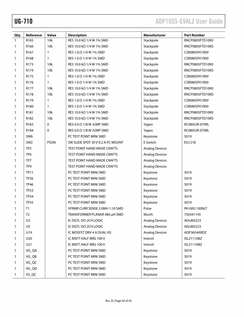
UG-710 ADP1055-EVALZ User Guide
Qty. Reference Value Description Manufacturer Part Number 1 R165 10k RES 10.0 kΩ 1/4 W 1% SMD Stackpole RNCP0805FTD10K0
1 R166 10k RES 10.0 kΩ 1/4 W 1% SMD Stackpole RNCP0805FTD10K0
1 R167 1 RES 1.0 Ω 1/4 W 1% SMD Stackpole CSR0805FK1R00
1 R168 1 RES 1.0 Ω 1/4 W 1% SMD Stackpole CSR0805FK1R00
1 R173 10k RES 10.0 kΩ 1/4 W 1% SMD Stackpole RNCP0805FTD10K0
1 R174 10k RES 10.0 kΩ 1/4 W 1% SMD Stackpole RNCP0805FTD10K0
1 R175 1 RES 1.0 Ω 1/4 W 1% SMD Stackpole CSR0805FK1R00
1 R176 1 RES 1.0 Ω 1/4 W 1% SMD Stackpole CSR0805FK1R00
1 R177 10k RES 10.0 kΩ 1/4 W 1% SMD Stackpole RNCP0805FTD10K0
1 R178 10k RES 10.0 kΩ 1/4 W 1% SMD Stackpole RNCP0805FTD10K0
1 R179 1 RES 1.0 Ω 1/4 W 1% SMD Stackpole CSR0805FK1R00
1 R180 1 RES 1.0 Ω 1/4 W 1% SMD Stackpole CSR0805FK1R00
1 R181 10k RES 10.0 kΩ 1/4 W 1% SMD Stackpole RNCP0805FTD10K0
1 R182 10k RES 10.0 kΩ 1/4 W 1% SMD Stackpole RNCP0805FTD10K0
1 R183 0 RES 0.0 Ω 1/8 W JUMP SMD Yageo RC0805JR-070RL
1 R184 0 RES 0.0 Ω 1/8 W JUMP SMD Yageo RC0805JR-070RL
1 SWA PC TEST POINT MINI SMD Keystone 5019
1 SW2 PSON SW SLIDE SPDT 30 V 0.2 A PC MOUNT E Switch EG1218
1 TP5 TEST POINT HAND MADE CRAFTS Analog Devices
1 TP6 TEST POINT HAND MADE CRAFTS Analog Devices
1 TP7 TEST POINT HAND MADE CRAFTS Analog Devices
1 TP9 TEST POINT HAND MADE CRAFTS Analog Devices
1 TP11 PC TEST POINT MINI SMD Keystone 5019
1 TP26 PC TEST POINT MINI SMD Keystone 5019
1 TP46 PC TEST POINT MINI SMD Keystone 5019
1 TP53 PC TEST POINT MINI SMD Keystone 5019
1 TP54 PC TEST POINT MINI SMD Keystone 5019
1 TP55 PC TEST POINT MINI SMD Keystone 5019
1 T1 XFRMR CURR SENSE 2.0MH 1:10 SMD Pulse PA1005.100NLT
1 T2 TRANSFORMER PLANAR 480 µH SMD Wurth 750341145
1 U2 IC DGTL ISO 2CH LOGIC Analog Devices ADuM3223
1 U5 IC DGTL ISO 2CH LOGIC Analog Devices ADuM3223
1 U19 IC MOSFET DRV 4 A DUAL HS Analog Devices ADP3654ARDZ
1 U20 IC MSFT HALF-BRG 100 V Intersil ISL2111ABZ
1 U21 IC MSFT HALF-BRG 100 V Intersil ISL2111ABZ
1 VG_QA PC TEST POINT MINI SMD Keystone 5019
1 VG_QB PC TEST POINT MINI SMD Keystone 5019
1 VG_QC PC TEST POINT MINI SMD Keystone 5019
1 VG_QD PC TEST POINT MINI SMD Keystone 5019
1 VS_QC PC TEST POINT MINI SMD Keystone 5019
Rev. B | Page 42 of 43
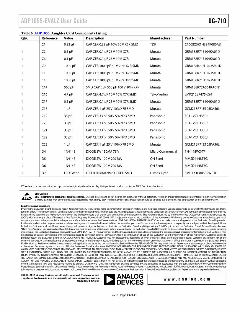
ADP1055-EVALZ User Guide UG-710 Table 6. ADP1055 Daughter Card Components Listing Qty. Reference Value Description Manufacturer Part Number
C1 0.33 µF CAP CER 0.33 µF 10% 50 V X5R SMD TDK C1608X5R1H334K080AB
1 C2 0.1 µF CAP CER 0.1 µF 25 V 10% X7R Murata GRM188R71E104KA01D
1 C6 0.1 µF CAP CER 0.1 µF 25 V 10% X7R Murata GRM188R71E104KA01D
1 C9 1000 pF CAP CER 1000 pF 50 V 20% X7R SMD Murata GRM188R71H102MA01D
1 C10 1000 pF CAP CER 1000 pF 50 V 20% X7R SMD Murata GRM188R71H102MA01D
1 C13 1000 pF CAP CER 1000 pF 50 V 20% X7R SMD Murata GRM188R71H102MA01D
1 C14 560 pF SMD CAP CER 560 pF 100 V 10% X7R Murata GRM188R72A561KA01D
1 C16 4.7 µF CAP CER 4.7 µF 10 V 10% X7R SMD Taiyo Yuden LMK212B7475KG-T
1 C17 0.1 µF CAP CER 0.1 µF 25 V 10% X7R SMD Murata GRM188R71E104KA01D
1 C18 1 µF CAP CER 1 µF 25 V 10% X7R SMD Murata GCM21BR71E105KA56L
1 C19 33 pF CAP CER 33 pF 50 V 5% NPO SMD Panasonic ECJ-1VC1H330J
1 C20 33 pF CAP CER 33 pF 50 V 5% NPO SMD Panasonic ECJ-1VC1H330J
1 C21 33 pF CAP CER 33 pF 50 V 5% NPO SMD Panasonic ECJ-1VC1H330J
1 C22 33 pF CAP CER 33 pF 50 V 5% NPO SMD Panasonic ECJ-1VC1H330J
1 C23 1 µF CAP CER 1 µF 25 V 10% X7R SMD Murata GCM21BR71E105KA56L
1 D4 1N4148 DIODE SW 150MA 75 V Micro Commercial 1N4448WX-TP
1 D5 1N4148 DIODE SW 100 V 200 MA ON Semi MMSD4148T3G
1 D6 1N4148 DIODE SW 100 V 200 MA ON Semi MMSD4148T3G
1 D7 LED Green LED THIN 660 NM SUPRED SMD Lumex Opto SML-LXT0805SRW-TR
I2C refers to a communications protocol originally developed by Philips Semiconductors (now NXP Semiconductors).
ESD Caution ESD (electrostatic discharge) sensitive device. Charged devices and circuit boards can discharge without detection. Although this product features patented or proprietary protection circuitry, damage may occur on devices subjected to high energy ESD. Therefore, proper ESD precautions should be taken to avoid performance degradation or loss of functionality.
Legal Terms and Conditions By using the evaluation board discussed herein (together with any tools, components documentation or support materials, the “Evaluation Board”), you are agreeing to be bound by the terms and conditions set forth below (“Agreement”) unless you have purchased the Evaluation Board, in which case the Analog Devices Standard Terms and Conditions of Sale shall govern. Do not use the Evaluation Board until you have read and agreed to the Agreement. Your use of the Evaluation Board shall signify your acceptance of the Agreement. This Agreement is made by and between you (“Customer”) and Analog Devices, Inc. (“ADI”), with its principal place of business at One Technology Way, Norwood, MA 02062, USA. Subject to the terms and conditions of the Agreement, ADI hereby grants to Customer a free, limited, personal, temporary, non-exclusive, non-sublicensable, non-transferable license to use the Evaluation Board FOR EVALUATION PURPOSES ONLY. Customer understands and agrees that the Evaluation Board is provided for the sole and exclusive purpose referenced above, and agrees not to use the Evaluation Board for any other purpose. Furthermore, the license granted is expressly made subject to the following additional limitations: Customer shall not (i) rent, lease, display, sell, transfer, assign, sublicense, or distribute the Evaluation Board; and (ii) permit any Third Party to access the Evaluation Board. As used herein, the term “Third Party” includes any entity other than ADI, Customer, their employees, affiliates and in-house consultants. The Evaluation Board is NOT sold to Customer; all rights not expressly granted herein, including ownership of the Evaluation Board, are reserved by ADI. CONFIDENTIALITY. This Agreement and the Evaluation Board shall all be considered the confidential and proprietary information of ADI. Customer may not disclose or transfer any portion of the Evaluation Board to any other party for any reason. Upon discontinuation of use of the Evaluation Board or termination of this Agreement, Customer agrees to promptly return the Evaluation Board to ADI. ADDITIONAL RESTRICTIONS. Customer may not disassemble, decompile or reverse engineer chips on the Evaluation Board. Customer shall inform ADI of any occurred damages or any modifications or alterations it makes to the Evaluation Board, including but not limited to soldering or any other activity that affects the material content of the Evaluation Board. Modifications to the Evaluation Board must comply with applicable law, including but not limited to the RoHS Directive. TERMINATION. ADI may terminate this Agreement at any time upon giving written notice to Customer. Customer agrees to return to ADI the Evaluation Board at that time. LIMITATION OF LIABILITY. THE EVALUATION BOARD PROVIDED HEREUNDER IS PROVIDED “AS IS” AND ADI MAKES NO WARRANTIES OR REPRESENTATIONS OF ANY KIND WITH RESPECT TO IT. ADI SPECIFICALLY DISCLAIMS ANY REPRESENTATIONS, ENDORSEMENTS, GUARANTEES, OR WARRANTIES, EXPRESS OR IMPLIED, RELATED TO THE EVALUATION BOARD INCLUDING, BUT NOT LIMITED TO, THE IMPLIED WARRANTY OF MERCHANTABILITY, TITLE, FITNESS FOR A PARTICULAR PURPOSE OR NONINFRINGEMENT OF INTELLECTUAL PROPERTY RIGHTS. IN NO EVENT WILL ADI AND ITS LICENSORS BE LIABLE FOR ANY INCIDENTAL, SPECIAL, INDIRECT, OR CONSEQUENTIAL DAMAGES RESULTING FROM CUSTOMER’S POSSESSION OR USE OF THE EVALUATION BOARD, INCLUDING BUT NOT LIMITED TO LOST PROFITS, DELAY COSTS, LABOR COSTS OR LOSS OF GOODWILL. ADI’S TOTAL LIABILITY FROM ANY AND ALL CAUSES SHALL BE LIMITED TO THE AMOUNT OF ONE HUNDRED US DOLLARS ($100.00). EXPORT. Customer agrees that it will not directly or indirectly export the Evaluation Board to another country, and that it will comply with all applicable United States federal laws and regulations relating to exports. GOVERNING LAW. This Agreement shall be governed by and construed in accordance with the substantive laws of the Commonwealth of Massachusetts (excluding conflict of law rules). Any legal action regarding this Agreement will be heard in the state or federal courts having jurisdiction in Suffolk County, Massachusetts, and Customer hereby submits to the personal jurisdiction and venue of such courts. The United Nations Convention on Contracts for the International Sale of Goods shall not apply to this Agreement and is expressly disclaimed.
©2014–2015 Analog Devices, Inc. All rights reserved. Trademarks and registered trademarks are the property of their respective owners. UG12386-0-4/15(B)
Rev. B | Page 43 of 43