Embed Size (px)
Citation preview
IEEE 2007 Custom Intergrated Circuits Conference (CICC)
Advanced Design Techniques forIntegrated Voltage Controlled LC Oscillators
Peter Kinget, Babak Soltanian*, Songtao Xu, Shih-an Yu, and Frank ZhangDept. of Electrical Engineering
Columbia UniversityNew York, NY 10027, USA.
*now with LSI Corporation, San Jose, CA 95134, USA.
Abstract-This paper reviews basic trade-offs in oscillator spurious coupling on the PCB. They further help to lower theperformance specifications. The better understanding of phase chip pin count and have become in widespread use.noise mechanisms as well as the availability of reliable phasenoise simulation tools has led to significant improvements in the Although oscillators have been designed as part of thepower-noise trade-off in recent years. It has further enabled the earliest electronic systems, they are still an area of intenseinvention of oscillator topologies which exhibit lower device research and innovation. Several recent advances in thenoise to phase noise conversion, and in this paper pulsed biasing understanding of phase noise generation (see e.g.,and its implementation through tail-current shaping is described [2][12][14][15]) in oscillators have created new opportunitiesas an example. Area reduction of LC oscillators is further to develop better VCO topologies. Furthermore, asinvestigated as the large size of oscillators' on-chip LC tank technology geometries shrink and device speeds increase,circuits is becoming a significant problem in deeply scaled SOC higher operating frequencies can be reached; or, at lowerdesigns which often require multiple on-chip oscillators. frequencies, more complex and better performing topologies
can be used. However, the area of inductors and thus that ofI. INTRODUCTION VCOs is not scaling significantly, and often several VCOs are
Oscillators are funda a bneeded on one complex SOC making the area reduction ofOscillators are fundamental building blocks in many VO hleg. W ics xmlso opcelectronic systems since they provide timing or frequency quadrature VCOtopoloeg es as well as the re-use of the realreference signals. Typically a fixed external reference estature O thei c to save rea.frequency is transformed into a programmable high frequencyclock or carrier signal with a phase locked loop (PLL). The We review some of the basic oscillator performancevoltage controlled oscillator (VCO) is a key building block for metrics and the design trade-offs that exist between them inthe PLL and determines several performance characteristics of section II and the device noise to phase noise conversionthe PLL. Even as technology features scale and more and mechanisms in section III. We then look at somemore functions are implemented in the digital domain, the opportunities for improving oscillator performance using pulseVCO remains a fundamental building block with no viable biasing in section IV and show how tail-current shaping offersdigital alternative for low jitter and low phase noise a compact implementation of such a topology in section V.applications. Section VI introduces design techniques for compact VCOs by
As the speed performance of devices in scaled re-using the area under the inductors.technologies improves, high speed serial I/O communications 1. OSCILLATOR DEsiGN TRADE-OFFSare proliferating which requires the realization of many on-chip VCOs on complex digital ICs. Modern wireless The design of an integrated VCO involves the trade-offofcommunication devices need to offer compatibility with a number of important design parameters. Operatingseveral standards which often requires operation over different frequency and phase noise requirements are set by the targetedfrequency bands using multiple integrated VCOs on a chip. application and the chosen transceiver architecture. TuningApplications requiring low jitter or low phase noise have to range requirements depend on specifications such asrely on harmonic oscillators since they offer much superior maximum time span of continuous locked operation as well asphase noise performance over relaxation or ring oscillators the anticipated variations in process, supply voltage and(see e.g., [2][3][4]). For the IGHz to several 10s of GHz temperature. The required supply rejection performancefrequency range, LC tanks can be integrated on-chip. largely depends on the environment and availability ofAlthough the quality of the on-chip tanks is inferior to off-chip dedicated supplies or supply regulators for the VCO.resonators, integrated GHz VCOs avoid issues such as The first order trade-offs between operation frequency,spurious resonances with package parasitics as well as phase noise performance and power consumption are well
1-4244-1623-X/07/$25.00 0C2007 IEEE 25-1-1 805
Authorized licensed use limited to: Columbia University. Downloaded on November 4, 2008 at 18:45 from IEEE Xplore. Restrictions apply.
C VCO < 2000 * VCO 2000-2006 A QVCO < 2000 0 QVCO 2000-2006
200.0
195.0 H
190.0 - .
185.0 a
I180.0 E U,
=175.0
170.0LL Q
165.0A.. A
160.0
155.0
150.00 2 4 6 8 10 12
Oscillation Freq. [GHz]
Figure 1 Figure of merit versus nominal oscillation frequency for different fully integrated VCO and quadrature VCO, QVCO, designsfrom the Journal of Solid State Circuits, the International Solid-State Circuits Conference, the Symposium on VLSI circuits, the European
Solid-State Circuits conference and Cuthsom Integrated Circuits Conference for the respective time periods.
understood. Starting with Leeson's model [1], which is based the Q2 scales with the area [7]. Consequently, the FOMon a approximate linear analysis of the noise in oscillators, a improves with the area of the inductor (and thus the oscillator)quadratic dependence of the phase noise on the operating and oscillators with different areas can be compared using anfrequency, fo, is predicted. More advanced phase noise FOMA [8] defined as:analysis methods [2][15] confirm this dependence.Furthermore the basic noise-power trade-off in an oscillator is =
0f lmW lmm2 (2)
similar to other circuits where the parallel connection of N FOMA =101og P(2identical oscillators leads to an N-times power increase for an ) L{fm} * P* A)improvement of the carrier-to-noise ratio by N. Theseobservations led to the following definition of a power-noise where A is the area of the oscillator (or tank).figure-of-merit [3] for an oscillator: Many other parameters play a role in the obtained power-
2 noise trade-off in an oscillator design. The choice of a
FOM = IO logl fo lm'(1W current-limited versus voltage-limited operation regionFOM = 1Olot~fmo) L{fm}P1 (1) keeping all other parameters equal affects the FOM [5]. The
elimination of bias elements such as the tail-current source in
wherefJo is the oscillation frequency, L/fm} is the SSB phase differential oscillators can improve the noise performance butnoise in dBc/Hz at an offset fm from the carrier and P is the increases the sensitivity to the power supply noise [6].power consumption. This FOM can be used to normalize an If large tuning ranges are required, it becomes moreoscillator's performance in order to compare oscillators with difficult to obtain a good power-noise trade-off. In a singledifferent operating frequencies, phase noise performance and oscillator the tank resonance frequency can typically onlypower consumption. effectively be tuned continuously using MOS or PN varactors
The quality factor, Q, of an integrated tank has the or discretely using switches and capacitors or switched
strongest effect on the performance of the VCO, where a varactors. To achieve a large tuning range a large tank
quadratic dependence of the phase noise on the tank's Q is capacitance, C, and a small tank inductance, L, has to be usedgenerally observed. For integrated oscillators the tank Q and consequently the tank impedance, Z0 = L IC = 2H fo,depends largely on the Q of the integrated inductors, although is small at the lower oscillation frequencies resulting in lowerat higher frequencies the reduction of the varactor Q can affect amplitudes and degraded phase noise performance. Thethe tank quality. However, high quality fixed capacitors are amplitude variation can be overcome by using constantusually available so that capacitive tapping can be used to amplitude biasing by e.g., using a mixed mode amplitudeimprove the varactor Q at the expense of extra area [3]. control loop [9], but at the cost of a varying phase noiseCapacitive tapping can further reduce the upconversion of low performance and power consumption. For very large tuningfrequency noise through AM-to-FM conversion in the ranges, several oscillators can be combined in parallel at avaractors. The Qofaninductor depends on the thickness and considerable expense in chip area [10]. Several parametersthe resistivity of the conductors, the substrate conductivity as play into the dependence of the noise-power trade-off inwell as the area used for the inductor layout. To the first order, oscillators on the tuning range and therefore a physics based
25-1-2 806
Authorized licensed use limited to: Columbia University. Downloaded on November 4, 2008 at 18:45 from IEEE Xplore. Restrictions apply.
definition of a FOM including the tuning range is difficult. Both approaches can offer the designer important insightsAn ad hoc FOM including the tuning range has been defined in making improvements in the oscillator topology to improvein [11]. the oscillator performance. As discussed earlier, some basic
Figure 1 shows the FOMs for fully integrated CMOS VCO power-noise trade-offs are set by physical constraints but the
designs published since 1994 in the solid-state circuit designer can improve the FOM by minimizing the device-designs published since 1994 in thesolid-state, c.r.u.i.noise-to-phase-noise conversion. For example, in [16], it wasliterature. The data is divided using two criteria: designs determined through frequency-domain phase-noise analysispublished before 1999 and included in a similar plot that was [15] that the largest phase noise contribution of the tail currentpublished in [3], and quadrature (QVCO) versus non- source comes from its thermal noise at the second harmonicquadrature oscillators (VCO). Two important trends can be and can be eliminated using an on-chip LC filter. In [2] andnoticed. Prior to 2000, QVCOs had a markedly inferior FOM [20], based on insights on how the shape of the ISF affects 1/fperformance than VCOs. Recent designs, however, have noise upconversion in oscillators, the use of time-domainsignificant better FOM, often on-par or exceeding VCO waveforms with symmetric rise and fall times was proposed todesigns. This is the result of numerous improvements in the reduce the effects of 1/f noise. Below we will illustrate howdesign and topologies of QVCOs. We further notice that there
i gisanoieal imrvmn inteFMo Csa el nsights gained from observing the 1SF function that the noise
injected at different times affects the phase and amplitudeWe will discuss the underlying factors in these improvements differently [2], led to the development of pulse biasing forin the upcoming sections and illustrate them with a couple of differential oscillators discussed in the next section.examples.
LC VCOs typically operate in large signal mode and areIII. DEVICE NOISE TO PHASE NOISE CONVERSION often designed to have maximum oscillation amplitude.
The calculation or simulation of the phase noise Sufficiently large oscillation amplitude is needed to drive theperformance of an oscillator is very involved since it requires other circuits such as mixers or dividers. A large VCO signalthe noise analysis of a strongly non-linear autonomous system alleviates the design challenges associated with the LO or[12]. Linear time-invariant noise analysis has been used to divider buffer. Additionally, from (3), one concludes that theobtain first-order approximations to gain understanding about phase noise improves with increasing oscillation amplitude.the trade-offs involved in oscillator design (see e.g. However, phase noise mechanisms exist that can degrade the[1][13][3]) but does not capture how strongly the device noise phase noise performance at large amplitudes, makingsources affect the amplitude versus the phase of the F increase substantially for larger amplitudes.oscillator's output. For most applications, the phase noise is k,eff,RMSof primary concern since the amplitude noise is largely The varactor diodes in a VCO are known to have strongeliminated through the use of amplitude-saturating buffers or AM-to-FM conversion [17]. 1/f or thermal noise of the tailmixers, although it can still be converted into phase noise bias source is upconverted to AM noise around the carrier [15]through AM-to-PM conversion in these circuits. Good but can be converted to frequency and phase noise by theagreement between experimental results and phase noise varactor. The AM-to-FM conversion gain of varactorspredictions is obtained by using a frequency-domain noise depends on their bias point, and at the edges, or in the middleanalysis including a detailed separation of the modulation of the tuning range this conversion can become small [17]. Ateffects of the noise on the amplitude versus the phase [14][15]. those points, the AM-to-FM conversion due to the signalAlternatively, using a time domain approach, the impulse dependent parasitic capacitors in the active elements of theresponse of an LC oscillator followed by a phase detector can negative resistance switching pair can become dominant [19].be determined for each noise source. To the first order, these The operation region of the MOS negative-resistance devicesnoise-to-phase impulse responses, a.k.a. impulse sensitivity changes periodically which modulates the parasiticfunctions (ISF), are linear and periodically time variant and capacitances. As a result, the effective tank capacitance andallow the calculation of the phase noise of an oscillator using consequently the oscillation frequency changes with respect to[2]: the oscillation amplitude for a fixed tuning voltage. In
differential MOS LC VCOs, the optimum differential2 amplitude is approximately equal to the threshold voltage ofn,k F2 the MOS devices, which corresponds to the minimum AM-to-Af k,eff,RMS FM conversion by the active devices. This effect is illustrated
Lffm } =10log 2A2C2 2 (3) by the measured results in Figure 2 for a tail-biased nMOSfm switching pair LC VCO where the phase noise exhibits an
optimum amplitude [19]. Similar experimental results haveJ been presented in [18].
where ink/Af is the power spectral density of the k-th AM-to-FM conversion is an important mechanism,n,k especially in oscillators with large tuning ranges. Also, incurrent noise source, r,Ff.M is effective value of the oscillators where noise mitigation design techniques havek,eff,RMS ~~~~been used, AM-to-FM conversion of AM noise often becomesassociated 1SF, A iS the oscillation amplitude and C iS the tank the limitin'g noise mechanism.capacitance.
We note that the availability of reliable phase noiseanalysis in several modern circuit simulators, which capture
25-1-3 807
Authorized licensed use limited to: Columbia University. Downloaded on November 4, 2008 at 18:45 from IEEE Xplore. Restrictions apply.
all of the effects described above, has become a significant tank at the right moment, i.e., when the voltage across the tankhelp for VCO designers and partially explains the progress in is maximum and the ISF is minimum. Some oscillators, suchVCO performance in recent years. as the Colpitt's oscillator have the property that the negative-
resistance active device only conducts when the output voltage10 is maximum [2]. Colpitt's oscillators however often need
1=1.77GHz larger bias currents to satisfy the start-up conditions than9 -0- f=1.9GHz differential pair based LC VCOs which are in widespread use.f=2.148GHz
:S 8 In [21] it is demonstrated that the phase noise of thedifferential NMOS LC VCO, shown in Figure 3, can be
0 improved by replacing the constant bias current Itail with aperiodic narrow pulse current source with the same average
X current. The current pulses must be aligned with the maximaand minima in the VCO output voltage and the frequency of
D9 40 X the periodic current source is twice the oscillation frequency.
Figure 4 shows the phase noise reduction achieved byX2 _ - using an rectangular current source implemented with an MOS
device compared to a constant current bias. Two mechanismsare involved in the phase noise reduction. Pulse biased VCOs
O 5 1 1.5 achieve a better DC-to-RF conversion and a larger oscillationDifferential oscillationarnplitude, 2A (V) amplitude compared to a fixed current biased VCO with the
Figure 2 Measured phase noise degradation with respect to the minimum same average current. Larger oscillation amplitude contributesvalue at a 600kHz offset for different amplitudes for a tail-biased nMOS to the phase noise reduction (see Figure 4(b)). Secondly, the
switching pair LC VCO. The 1.77GHz, 1.9GHz, and 2.148GHz oscillation effective ISFs for the current noise of the switching pair andfrequencies correspond to a tuning voltage at the edges and in the middle of the tail current source are reduced since they only conduct for
the tuning range where the varactor AM-to-FM conversion is minimal very short periods at the least phase sensitive times. The phase
noise improves for narrower current pulses (smallervdd tconductions angle) where in the limit they become impulses.
One caveat is that although pulsed biasing can make sure that1 L L R device noise is more converted into amplitude noise than
V-<!A 7lue i 4; 1i, phase noise, some of the amplitude noise can still beI | .k1g I 1g 1 . | | converted into phase noise through AM-to-FM conversion in
c c1 the VCO as discussed earlier.Vo,n0:}-oP (a) total phase noise reduction
ZM 2 Id4MlJ..E
t t M Eh _t 0
v2 5_ 5}v i W ) 9 a 10 0 5 1 15 2 2M5 3- | ~~~~~~~~~~~~~~~~~~~~~Conducion angIe 2¢ [radians]
4~~ ~ ~~~~~~~~~~~~~~ ...
~~~~~~~~~~~~~~~~~~~~~~(b) phaEsElenisreduction beakdot}wn
_~~~~~~~~~~~~~~ ,
Figure 3 Schematic ofadifferential NMOSLCVCO 1t:
IV. PULSE BIASING OscillAgg,ttl...Tioam*t. . *,.. X coupled+Tail deviceslThe phase change in the VCO output in response to a noise 2
*- ** r00.5 1 15 2.5 3current pulse injected into the tank depends on the instant Of Conduction angle 2 [radians]injection in the oscillation cycle and is a periodic functionknown as the impulse sensitivity function (1SF) [2]; the 1SF is Figure 4 Phase noise reduction in a pulse biased differential NMOS LCtypically maximum when the output voltage is at the zero- vco; (a) total phase noise reduction versus conduction angle; (b) respective
crossing instants andit is minimum when the output.voltage is contributions of higher oscillation amplitude and lowerISF in the phase
at itS maximum or minimum value. In order to overcome the nierdcinloss in the LC tank, the active part of the VCO needs to injectcurrent into the tank to maintain the oscillation, but alsoinjects noise. Looking at (3), we note that the contribution ofa device noise source to the phase noise can be reduced byreducing the effective 1SF FeV RMS The resulting phase
noise can thus be reduced if the current is injected into the
25-1-4 808
Authorized licensed use limited to: Columbia University. Downloaded on November 4, 2008 at 18:45 from IEEE Xplore. Restrictions apply.
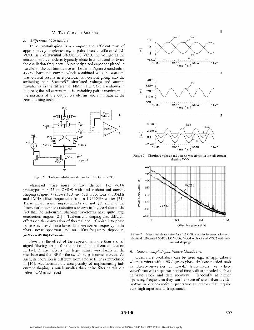
V. TAIL CURRENT SHAPING WVotp Vo,n
A. Differential Oscillators 1t 9Tail-current-shaping is a compact and efficient way of 1.5
approximately implementing a pulse biased differential LC >VCO. In a differential NMOS LC VCO, the voltage at the r Vscommon-source node is typically close to a sinusoid at twice 700mthe oscillation frequency. A properly sized capacitor placed in 40On 404n ( 40s 8 41.2parallel to the tail bias device as shown in Figure 5 conducts asecond harmonic current which combined with the constantbias current results in a periodic tail current going into theswitching pair. SpectreRF simulated voltage and current 8 -waveforms in the differential NMOS LC VCO are shown in 830rnFigure 6; the tail current into the switching pair is maximum at > 820mthe maxima of the output waveforms and minimum at the 810mzero-crossing instants.
800m40.0n 40.4n 40.8n 41.2n
time ( s_ _ ~~~~~~~~~Peak _ _Detector 1
V0,P ~~~~~~~~~~~4,OmnVtune HE0 FV, _ oA0 g
Von Vo f 2.Om aVdd aIdl S t WtXSkJdZ0.0
C
Mref 120/0.25 Vs 1,20/0.25 -2.0m46.0n 40.4n 40.8n 41.2nItail time s )
lmbis r4lk Figure 6 Simulated voltage and current waveforms in the tail-current-M3hli3as Cp=8pF shaping VCO.150/1
Figure 5 Tail-current-shaping differential NMOS LC VCO.-90I
Measured phase noise of two identical LC VCOs l ai Vprototypes in 0.25um CMOS with and without tail currentshaping (Figure 7) shows 3dB and 5dB reductions at l00kHz * -l10 _ -and 1MHz offset frequencies from a 1.755GHz carrier [21].These phase noise improvements do not yet achieve the = - - - ltheoretical maximum reductions shown in Figure 4 due to the Lfact that the tail-current shaping waveforms have quite largeconduction angles [21]. Tail-current shaping has different -140effects on the conversion of thermal and 1/f noise into phase 10k 100k IM 10Mnoise which results in a lower 1/f noise corner frequency in the Offset Frequency (Hz)phase noise spectrum and an offset-frequency dependentphase noise improvement. Figure 7 Measured phase noise for a 1.755GHz carrier frequency for two
identical differential NMOS LC VCOs; VCO1 without and VC02 with tail-Note that the effect of the capacitor is more than a small current shaping.
signal filtering action for the noise of the tail current source.In fact, it also affects the large signal waveforms in the B. Source-coupled Quadrature Oscillatorsoscillator and the ISF for the switching pair noise sources. Assuch, its operation is different from a noise filter as introduced .Quadrature oscillators can be used e.g. in applicationsin [16] Adiinly the are penlt of implementingtail where carriers with a 90 degrees phase shift are needed suchcurent . sApiongsu mlthea no fimlteing hile as direct-conversion or low-IF transceivers, or wherebenterFOM is achieved waveforms with a quarter-period time shift are needed such ashalf-rate clock and data recovery. Especially at higher
operating frequencies they can be more efficient than divide-by-two or divide-by-four quadrature generators that requirevery high input carrier frequencies.
25-1-5 809
Authorized licensed use limited to: Columbia University. Downloaded on November 4, 2008 at 18:45 from IEEE Xplore. Restrictions apply.
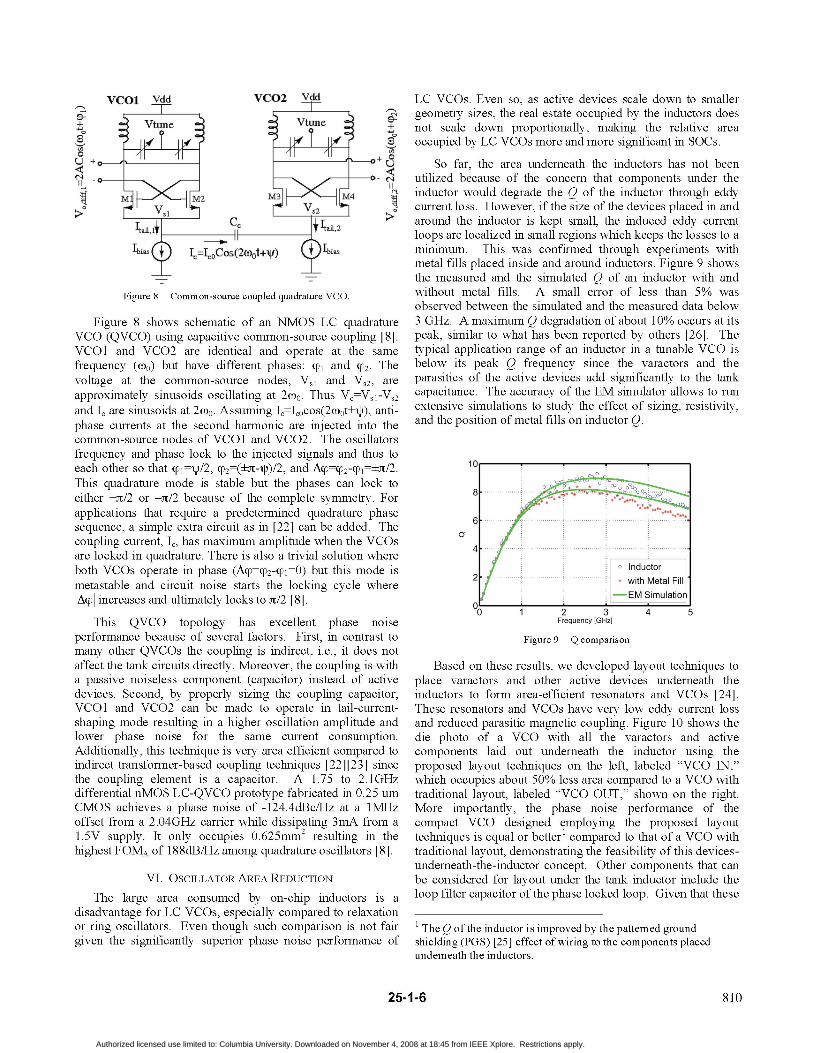
VCO1 Vdd VCO2 Vdd LC VCOs. Even so, as active devices scale down to smaller1.VI-- Vt=ne E geometry sizes, the real estate occupied by the inductors does
->m + 11111-' gi \'t,ll, a not scale down proportionally, making the relative areau T$ occupied by LC VCOs more and more significant in SOCs.u 4*_ u So far, the area underneath the inductors has not been
0- c-" utilized because of the concern that components under the
M M2MX M4hki ; rinductor would degrade the Q of the inductor through eddy2rl n1 r r l Ys> current loss. However, if the size of the devices placed in and>. i1 cc 1+42 > around the inductor is kept small, the induced eddy current
Ttaiii loops are localized in small regions which keeps the losses to a
ibi ) k,=I,0Cos(2o0t+Nf) Ibiw minimum. This was confirmed through experiments withmetal fills placed inside and around inductors. Figure 9 showsthe measured and the simulated Q of an inductor with and
Figure 8 Common-source coupled quadrature VCO. without metal fills. A small error of less than 5% wasobserved between the simulated and the measured data below
Figure 8 shows schematic of an NMOS LC quadrature 3 GHz. A maximum Q degradation of about 10% occurs at itsVCO (QVCO) using capacitive common-source coupling [8]. peak, similar to what has been reported by others [26]. TheVCO1 and VC02 are identical and operate at the same typical application range of an inductor in a tunable VCO isfrequency (co) but have different phases: cpi and cP2. The below its peak Q frequency since the varactors and thevoltage at the common-source nodes, Vs, and Vs2, are parasitics of the active devices add significantly to the tankapproximately sinusoids oscillating at 2co. Thus Vc=Vsl-Vs2 capacitance. The accuracy of the EM simulator allows to runand Ic are sinusoids at 2co. Assuming Ic=Icocos(2oot+V), anti- extensive simulations to study the effect of sizing, resistivity,phase currents at the second harmonic are injected into the and the position of metal fills on inductorQcommon-source nodes of VCO1 and VC02. The oscillatorsfrequency and phase lock to the injected signals and thus toeach other so that cpr=p/2, cp2=(+m-V)/2, and Acp=cp2-cp1i=±/2. ICThis quadrature mode is stable but the phases can locktoForeither +mT/2 or -mT/2 because of the complete symmetry. Forapplications that require a predetermined quadrature phase rsequence, a simple extra circuit as in [22] can be added. Thecoupling current, Ic, has maximum amplitude when the VCOsare locked in quadrature. There is also a trivial solution whereboth VCOs operate in phase (Acp=cP2-cP1=0) but this mode is inductrmetastable and circuit noise starts the locking cycle where 2 wthetal FlkAcp increases and ultimately locks to m/2 [8]. _
o 1 2 3 4 5This QVCO topology has excellent phase noise Frequency [GHz]
performance because of several factors. First, in contrast to Figure 9 Q comparisonmany other QVCOs the coupling is indirect, i.e., it does notaffect the tank circuits directly. Moreover, the coupling is with Based on these results, we developed layout techniques toa passive noiseless component (capacitor) instead of active place varactors and other active devices underneath thedevices. Second, by properly sizing the coupling capacitor, inductors to form area-efficient resonators and VCOs [24].VCO1 and VC02 can be made to operate in tail-current- These resonators and VCOs have very low eddy current lossshaping mode resulting in a higher oscillation amplitude and and reduced parasitic magnetic coupling. Figure 10 shows thelower phase noise for the same current consumption. die photo of a VCO with all the varactors and activeAdditionally, this technique is very area efficient compared to components laid out underneath the inductor using theindirect transformer-based coupling techniques [22][23] since proposed layout techniques on the left, labeled "VCO IN,"the coupling element is a capacitor. A 1.75 to 2.1GHz which occupies about 50% less area compared to a VCO withdifferential nMOS LC-QVCO prototype fabricated in 0.25 um traditional layout, labeled "VCO OUT," shown on the right.CMOS achieves a phase noise of -124.4dBc/Hz at a lMHz More importantly, the phase noise performance of theoffset from a 2.04GHz carrier while dissipating 3mA from a compact VCO designed employing the proposed layout1.5V supply. It only occupies 0.625mm2 resulting in the techniques is equal or better1 compared to that of a VCO withhighest FOMA of 1 88dB/Hz among quadrature oscillators [8]. traditional layout, demonstrating the feasibility of this devices-
underneath-the-inductor concept. Other components that canVI. OSCILLATOR AREA REDUCTION be considered for layout under the tank inductor include the
The large area consumed by on-chip inductors is a loop filter capacitor ofthe phase locked loop. Given that thesedisadvantage for LC VCOs, especially compared to relaxationor ring oscillators. Even though such comparison is not fair lThe Q of the inductor is improved by the patterned groundgiven the significantly superior phase noise performance of shielding (PGS) [251 effect of wiring to the components placed
underneath the inductors.
25-1-6 810
Authorized licensed use limited to: Columbia University. Downloaded on November 4, 2008 at 18:45 from IEEE Xplore. Restrictions apply.
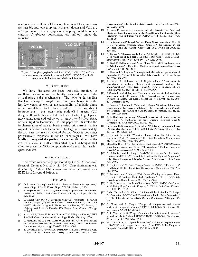
components are all part of the same functional block, concerns Upconversion," IEEE J. Solid-State Circuits, vol. 37, no. 8, pp. 1003-for possible spurious coupling with the inductor and VCO are o011, Aug. 2002not significant. However, spurious coupling could become a [7] J. Crols, P. Kinget, J. Craninckx and M. Steyaert, "An Analytical
concern. arbitrarycomponents are laid-outunderthe Model of Planar Inductors on Lowly Doped Silicon Substrates for High
Frequency Analog Design up to 3GHz," in VLSI Symposium, 1996,inductor. pp. 28-29.
[8] B. Soltanian, and P. Kinget, "A Low Phase Noise Quadrature LC VCOUsing Capacitive Common-Source Coupling", Proceedings of theEuropean Solid-State Circuits Conference (ESSCIRC), Sept. 2006, pp.436-439.
[9] A. Bemyr, A. Niknejad, andR. Meyer, "A 1.8-GHz LC VCO wi 1.3-GHz tuning range and digital amplitude calibration," IEEE J. Solid-State Circuits, vol. 40, no. 4, pp. 909-917, April 2005.
[10] A. Kral, F. Behbahani, and A. A. Abidi, "Re-CMOS oscillators withswitched tuning," in Proc. IEEE Custom Integrated Circuits Conference(CICC , 1998, pp. 555-558.
Figure 10 Die photograph of a traditional VCO, "VCO OUT", with no [11] D. Ham and A. Hajimiri, "Concepts and Methods in Optimization ofcomponents undereath the inductor and a VCO. "VCO IN", with all Integrated LC VCOs," IEEE J. Solid-State Circuits, vol. 36, no. 6, pp.
components laid out underneath the tank inductor. 896-909, June 2001[12] A. Demir, A. Mehrotra, and J. Roychowdhury, "Phase noise in
oscillators: a unifying theory and numerical methods forVII. CONCLUSIONS characterization," IEEE Trans. Circuits Syst. I, Fundam. Theory
We have discussed the basic trade-offs involved in Applicat., vol. 47, no. 5, pp. 655-674, May 2000.oscillator design as well as briefly reviewed some of the [13] J. Craninckx and M. Steyaert, "Low noise voltage-controlled oscillators
critical Cusing enhanced LC tanks," IEEE Transactions on Circuits andcritical p shasenoisnemehanisms. The bueotterunderstanding Systems-I1: Analog and Digital Signal Processing, vol. 42, pp. 794-that has developed through numerous research results in the 804, December 1995.last few years, as well as the availability of reliable phase [14] C. Samori, A. Lacaita, F. Villa, and F. Zappa, "Spectrum folding andnoise simulation tools has resulted in a significant phase noise in LC tuned oscillators," IEEE Transactions on Circuitsimprovement in the power-noise trade-off in recent VCO and Systems -tu i Analog and Digital Signal Processing, vol. 45, pp.
designs. It has further enabled a better understanding of phase 781-790, July 1998.[15] J. J. Rael and A. Abidi, "Physical processes of phase noise in
noise generation andoffers opportunities todevelopphase differential LC oscillators," in Proc. Custom Integrated Circuitsnoise mitigation techniques. In this paper we illustrated the Conference (CICC), May 2000, pp. 569-572.implementation of pulsed biasing using tail current shaping [16] E. Hegazi, H. Sjoland, and A. A. Abidi, "A filtering technique to lowercapacitors as one such technique. The large area occupied by LC oscillator phase noise," IEEE J. Solid-State Circuits, vol. 36, no. 12,the LC tank resonators required for LC VCO is becoming pp. 1921-1930, Dec. 2001.progressively expensive in scaled technologies. We have [17] E. Hegazi, A. Abidi, "Varactor Characteristics, Oscillator Tuning
brieflyinvestiNthe performance trade-offs related to the Curves, and AM-FM Conversion," IEEE J. of Solid-State Circuits, Vol.
brieaofly VCOi gatwed lasillstratedlyo t 38, No. 6, pp. 103 -103 , June 2003.are of aVCeson, Aswemplemlas il edbac osclayoutotechniques [18] Miyashita, D. et al, "A phase noise minimization of CMOS VCOs overallow to place the VCO components underneath the on-chip wide tuning range and large PVT variations," Custom Integratedspiral inductor. Circuits Conference, pp. 583-586, Sept. 2005.
[19] B. Soltanian and P. Kinget, "AM-FM Conversion by the ActiveACKNOWLEDGMENT Devices in MOS LC-VCOs and its Effect on the Optimal Amplitude,"
IEEE Radio Frequency Integrated Circuits Conference (FIC), 4 pp.,This work was partially sponsored by the SRC Sponsored June 2006.
Research Contract No. 2004-HJ-1 191. Chip fabrication was [20] A. Haj'imiri and T. Lee, "Design Issues in CMOS Differential LCdonated by Philips. EM simulations were performed with Oscillators," IEEE J. Solid-State Circuits, vol. 34, no. 5, pp. 717-724,
EMXcfrom Integrand Software. May 1999.[21] B. Soltanian and P. Kinget, "Tail Current-Shaping to Improve Phase
Noise in LC Voltage Controlled Oscillators," IEEE J. Solid-StateREFERENCES Circuits, vol. 41, no. 8, pp. 1792-1802, Aug.2006.
[4] D. A.eAbidi, "Pasimple moiseland Jittedbacki MOS scillat spectrum," [22] . Gierkink et al., "A Low-Phase-Noilse 5-GHz CMOS QuadratureProceedings of the IEEE, vol. 54, pp. 329-330, February 1966. VCo sing Si-barmonRFC's," IEEE J. Solid-State Circuits,
[2] A. Hajimiri and T. Lee, "A general theory of phase noise in electrical pp. 1148-1154, 2003.OCllators," IEEE J. Sold-State Circuits, vol. 33, no. 2, pp. 179-194, [23] C.-W. Yao and A. N. Willson, "A Phase-Noise Reduction TechniqueFeb. 1998 for Quadrature LC-VCO with Phase-to-Amplitude Noise Conversion,"Feb. 1998. ~~~~~~~~~~~~~~inIEEE International Solid-State Circuits Conference, 2006, pp. 196-
[3] P. Kinget, "Integrated GHz voltage controlled oscillators," in Analog 17Circuit Design: (X)DSL and Other Communication Systems; RkM 19
MO]STMvniodetals; Interaede FterndeOscillators,WCuransee [24] F. Zhang and P. Kinget, "Design of components and circuitsHujin,ad .vn ePasce Es oso,MA lwe,199Ip underneath integrated inductors," IEEE J. Solid-State Circuits, vol. 41,
353-381.R vnd lash,Ed.Bstn A Kue,199 p
no. 10, pp. 2265-2271, Oct. 2006.[4] . A Abdi,Phae Nise nd ittr i CMO Rig Ocilltor," EEE [25] C. P. Yue and S. S. Wong, "On-chip spiral inductors with patterned
[5] P.A.ndreani, "Pand A. isFard,"MotreontheS1/ ngPh secNiselPerormanc 33Io.5Ep.7375,MyE98
[6] 5.Levantno etal., "requeny Depndenceon Bia Currnt in -GHzrntegatd Cirecui (rF`IC)n,e pp. 3C85-38, JuFF I"n.2002. ,Cirmq c
CMOS VCOs: Impact on Tuning Range and Flicker Noise
25-1-7 811
Authorized licensed use limited to: Columbia University. Downloaded on November 4, 2008 at 18:45 from IEEE Xplore. Restrictions apply.