Embed Size (px)
Citation preview
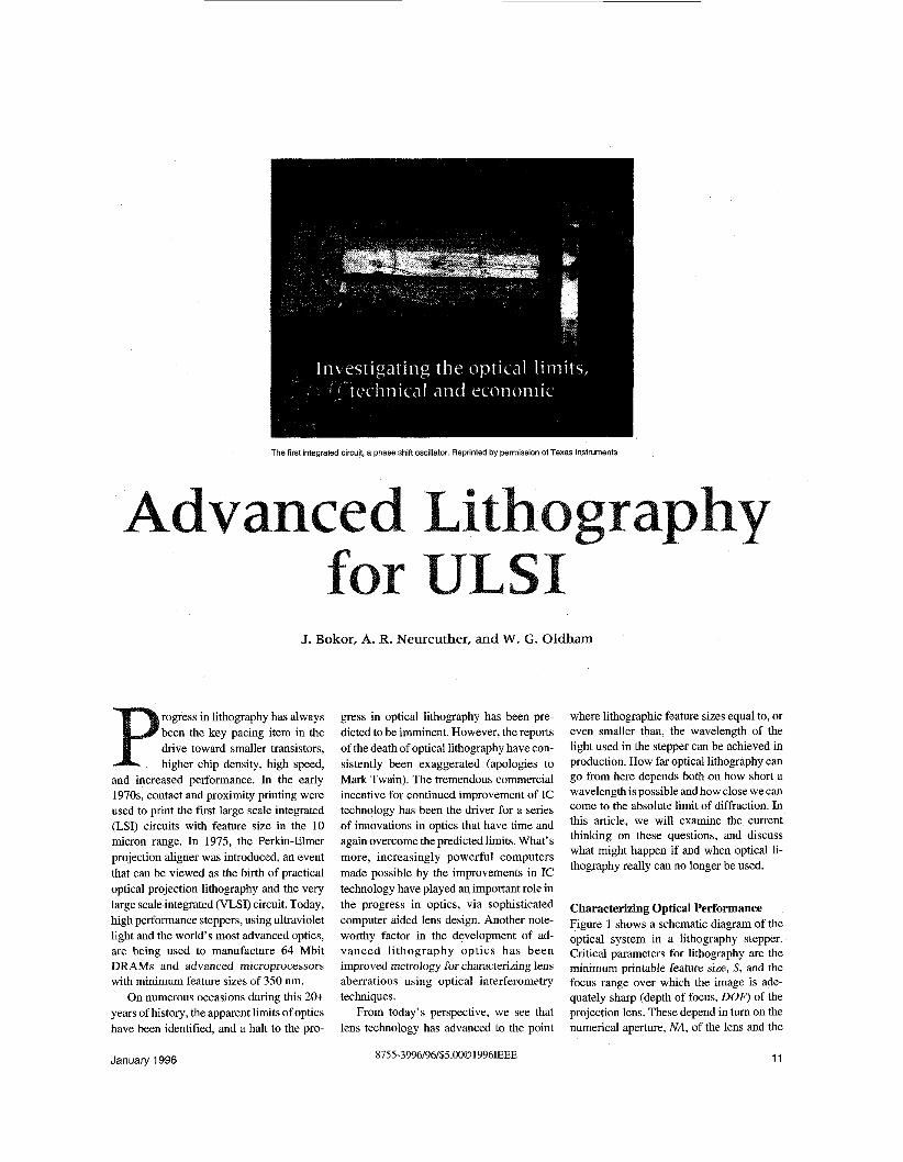
The first integrated circuit, a phase shift oscillator. Reprinted by permission of Texas Instruments
J. Bokor, A. R. Neureuther, and W. G. Oldham
rogress in lithography has always been the key pacing item in the drive toward smaller transistors, higher chip density, high speed,
and increased performance. In the early 1970s, contact and proximity printing were used to print the first large scale integrated (LSI) circuits with feature size in the 10 micron range. In 1975, the Perkin-Elmer projection aligner was introduced, an event that can be viewed as the birth of practical optical projection lithography and the very large scale integrated (VLSI) circuit. Today, high performance steppers, using ultraviolet light and the world’s most advanced optics, are being used to manufacture 64 Mbit DRAMS and advanced microprocessors with minimum feature sizes of 350 nm.
On numerous occasions during this 20+ years of history, the apparent limits of optics have been identified, and a halt to the pro-
gress in optical lithography has been pre- dicted to be imminent. However, the reports of the death of optical lithography have con- sistently been exaggerated (apologies to Mark Twain). The tremendous commercial incentive for continued improvement of IC technology has been the driver for a series of innovations in optics that have time and again overcome the predicted limits. What’s more, increasingly powerful computers made possible by the improvements in IC technology have played an important role in the progress in optics, via sophisticated computer aided lens design. Another note- worthy factor in the development of ad- vanced lithography optics has been improved metrology for characterizing lens aberrations using optical interferometry techniques.
From today’s perspective, we see that lens technology has advanced to the point
8755-3996/96/$5.0001996IEEE
where lithographic feature sizes equal to, or even smaller than, the wavelength of the light used in the stepper can be achieved in production. How far optical lithography can go from here depends both on how short a wavelength is possible and how close we can come to the absolute limit of diffraction. In this article, we will examine the current thinking on these questions, and discuss what might happen if and when optical li- thography really can no longer be used.
Characterizing Optical Performance Figure 1 shows a schematic diagram of the optical system in a lithography stepper. Critical parameters for lithography are the minimum printable feature size, S, and the focus range over which the image is ade- quately sharp (depth of focus, DOF) of the projection lens. These depend in turn on the numerical aperture, NA, of the lens and the
January 1996 11
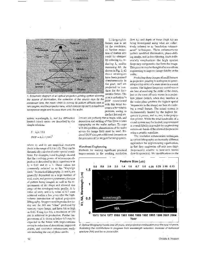
1. Schematic diagram of an optical projection printing system showing the source of illumination, the collection of the source rays by the condenser lens, the mask which to convey its pattern diffracts rays at new angles, and the projection lens, which collects ray out to a maximum acceptance angle and focuses them onto the wafer.
actinic wavelength, h, and for diffraction limited (ideal) optics are described by the simple relations:
S = k l h / N A
DOF = k2h I (NA)2
where kl and k2 are empirical constants (both in the range of 0.5 to 1 .O). They can be theoretically calculated under special condi- tions. For example, Lord Rayleigh showed that the resolving power of microscope ob- jectives is described by these equations with k1 = 0.61 and k2 = 1. These values are commonly referred to as the “Rayleigh limit.” In practical lithography, ki and kz are generally dependent on a large number of tool, resist, and process parameters, the type of pattern being imaged, as well as the re- quirements of the shape and allowed size range of the developed resist profile. A kr value of unity and a kz value of 0.7 were achieved within a few years after the high- volume introduction of optical projection lithography. Steppers used in production to- day use the 365 nm “i-line” produced by mercury vapor lamps, and have NA as high as 0.65. Using k1= 0.6, a resolution of 350 nm is achieved in production. Further im- provement of k1 down to below 0.5 may be expected in the future with improvements owing to reduction of aberrations, improved resists, and resolution enhancement meth- ods including the use.of phase masks.
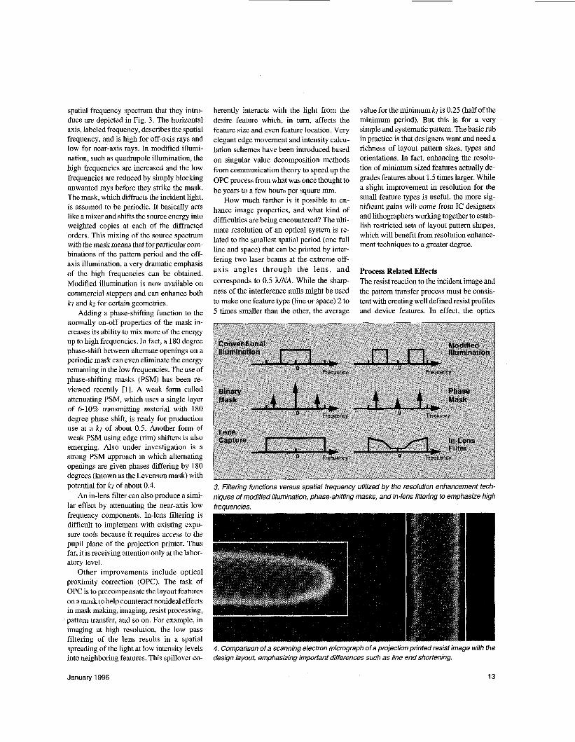
L i thographic feature size is set by the resolution, so further reduc- tion of feature size could be obtained by reducing kl , re- ducing h, andlor increasing NA. As shown in Fig. 2, all th ree s t ra tegies have been pursued simultaneously in the past, and are projected to con- tinue for the fore- seeable future. The severe seduction in
DUF assoc ia ted with this trend be- comes a formidable problem, owing to the fact thatreal wa-
fers are not perfectly flat to begin with, and deposition and etching of thin films creates topography on the wafer surface. To cope with this problem, planarization of the wafer across the image field must be used. Re- duced DOF also puts additional demands on the precision of the stepper focusing system.
Wavefront Engineering Methods for making significant practical improvements in the working resolution
(low k l ) and depth of focus (high kz) are being investigated using what are collec- tively referred to as “resolution enhance- ment” techniques. These enhancements include modified illumination, phase-shift- ing masks, and in-lens filtering. Each delib- erately emphasizes the high spatial frequency components that form the image. This process may be thought of as wavefront engineering to improve image fidelity at the wafer.
Producing sharp images of smkl features in projection printing is analogous to gener- ating a crisp strike of a snare drum in a sound system. The highest frequency sound waves are best at resolving the strike of the drum, just as the most off-axis waves in a projec- tion printer (which, when they interfere at the wafer plane produce the highest spatial frequencies in the image) are best at resolv- ing a small feature. The sound system is fundamentally limited by the highest fre- quency it passes, and so, too, is the projec- tion printer. While the total bandwidth of a sound system may be limited, improvement in overall fidelity is possible by emphasizing certain sub-bands of the allowed frequencies using a graphic equalizer.
The resolution enhancement techniques in optical lithography are basically different approaches for implementing equalization, in that they emphasize off-axis rays (high frequencies) relative to near-axis waves (low frequencies). The modifications to the
Feature Size (pm)
8.0 5.0 3.0 2.0 1.4 1.0 0.7 0.5 0.35 0.25 0.18 0.13
” 197119741977198019831986198919921995199820012004
Year
2. Optical lithography trends over 25 years, andprojected continuation over the next 10 years, illustrating the contributions to progress from wavelength reduction, increase of numerical aperture (NA) and the kr parameter.
12 Circuits & Devices
spatial frequency spectrum that they intro- duce are depicted in Fig. 3. The horizontal axis, labeled frequency, describes the spatial frequency, and is high for off-axis rays and low for near-axis rays. In modified illumi- nation, such as quadrupole illumination, the high frequencies are increased and the low frequencies are reduced by simply blocking unwanted rays before they strike the mask. The mask, which diffracts the incident light, is assumed to be periodic. It basically acts like a mixer and shifts the source energy into weighted copies at each of the diffracted orders. This mixing of the source spectrum with the mask means that for particular com- binations of the pattern period and the off- axis illumination, a very dramatic emphasis of the high frequencies can be obtained. Modified illumination is now available on commercial steppers and can enhance both kz and k2 for certain geometries.
Adding a phase-shifting function to the normally on-off properties of the mask in- creases its ability to mix more of the energy up to high frequencies. In fact, a 180 degree phase-shift between alternate openings on a periodic mask can even eliminate the energy remaining in the low frequencies. The use of phase-shifting masks (PSM) has been re- viewed recently [l]. A weak form called attenuating PSM, which uses a single layer of 6-10% transmitting material with 180 degree phase shift, is ready for production use at a kl of about 0.5. Another form of weak PSM using edge (rim) shifters is also emerging. Also under investigation is a strong PSM approach in which alternating openings are given phases differing by 180 degrees (known as the Levenson mask) with potential for kz of about 0.4.
An in-lens filter can also produce a simi- lar effect by attenuating the near-axis low frequency components. In-lens filtering is difficult to implement with existing expo- sure tools because it requires access to the pupil plane of the projection printer. Thus far, it is receiving attention only at the labor- atory level.
Other improvements include optical proximity correction (OPC). The task of OPC is to precompensate the layout features on a mask to help counteract nonideal effects in mask making, imaging, resist processing, pattern transfer, and so on. For example, in imaging at high resolution, the low pass filtering of the lens results in a spatial spreading of the light at low intensity levels into neighboring features. This spillover co-
herently interacts with the light from the desire feature which, in turn, affects the feature size and even feature location. Very elegant edge movement and intensity calcu- lation schemes have been introduced based on singular value decomposition methods from communication theory to speed up the OPC process from what was once thought to be years to a few hours per square mm.
How much farther is it possible to en- hance image properties, and what kind of difficulties are being encountered? The ulti- mate resolution of an optical system is re- lated to the smallest spatial period (one full line and space) that can be printed by inter- fering two laser beams at the extreme off- axis angles through the lens , and corresponds to 0.5 UNA. While the sharp- ness of the interference nulls might be used to make one feature type (line or space) 2 to 5 times smaller than the other, the average
value for the minimum kz is 0.25 (half of the minimum period). But this is for a very simple and systematic pattern. The basic rub in practice is that designers want and need a richness of layout pattern sizes, types and orientations. In fact, enhancing the resolu- tion of minimum sized features actually de- grades features about l .5 times larger. While a slight improvement in resolution for the small feature types is useful, the more sig- nificant gains will come from IC designers and lithographers working together to estab- lish restricted sets of layout pattern shapes, which will benefit from resolution enhance- ment techniques to a greater degree.
Process Related Effects The resist reaction to the incident image and the pattern transfer process must be consis- tent with creating well defined resist profiles and device features. In effect, the optics
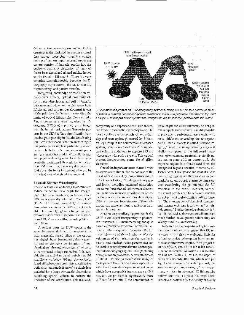
3. Filtering functions versus spatial frequency utilized by the resolution enhancement tech- niques of modified illumination, phase-shifting masks, and in-lens filtering to emphasize high frequencies.
4. Comparison of a scanning electron micrograph of a projection printed resist image with the design layout, emphasizing important differences such as line end shoflening.
January 1996 13
deliver a sine wave approximation to the openings in the mask and the chemistry must then convert these sine waves into square resist profiles. An important final step is the pattern transfer of the resist profile into the device structure. A discussion of many of the resist material and related etching issues can be found in [2] and [3]. There is a very complex interrelationship between the li- thography exposure tool, the resist material, its processing, and pattern transfer.
Integrating knowledge of resolution en- hancement effects, optical proximity ef- fects, resist dissolution, and pattern transfer into an overall view point which spans both IC design and process development is one of the principle challenges in extending the limits of optical lithography. For example, Fig. 4 compares. a scanning electron mi- crograph (SEM) of a printed resist image with the initial mask pattern. The resist pat- tern in the SEM differs significantly from the design, especially in that the terminating line is foreshortened. The foreshortening in this particular example is particularly severe because both the optics and the resist proc- essing contributions add. While IC design and process development have been suc- cessfully partitioned through the introduc- tion of design rules, the savvy designer still looks over the fence to find out what can be exploited and what should be avoided.
Towards Shorter Wavelengths Intense research is underway to continue to reduce the actinic wavelength for lithogra- phy. The wavelength region below about 300 nm is generally referred to “deep UV” (DUV). Efficient, powerful, ultraviolet lamps that operate in the DUV are not avail- able. Fortunately, gas-discharge pumped excimer lasers offer high powers at a selec- tion of DUV wavelengths, including 248 nm and 193 nm.
A serious issue for DUV optics is the severely restricted choice of transparent op- tical materials. Fused silica is the optical material of choice because of its homogene- ity and its desirable combination of me- chanical and $thermal properties, allowing it to be polished to high perfection. It is suit- able for use at 248 nm, and probably at 193 nm. However, below 193 nm, absorption in fused silica becomes prohibitive. Refractive optical systems made from only a singlelens material have large chromatic aberrations, requiring special efforts to narrow the linewidth of the laser source. This task adds
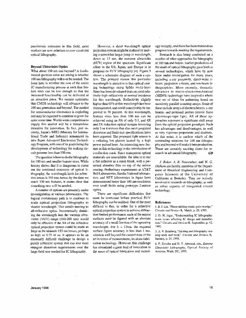
I EUV multilayer-coated
5. Schematic diagram of an EUV lithography system showing a laser-plasma source of 13 nm radiation, a Fmirror condenser system, a reflection mask with patterned absorber on top, and a simple 2-mirror projection system that images the mask absorber pattern onto the wafer.
complexity and expense to the laser source, and tends to reduce the available power. The mostly-reflective approach of reduction step-and-scan optics, pioneered by Silicon Valley Group in the commercial Micrascan system, is far more color tolerant. A signifi- cant effort is underway to explore 193 nm lithography with such a system. This optical system incorporates some fused silica elements.
One of the important issues that still must be addressed is that radiation damage of the fused silica is caused by long-term exposure to 193 nm radiation. This damage takes sev- eral forms, including enhanced absorption due to the formation of color center defects, and radiation induced densification (com- paction), which can induce lens aberrations. Efforts to develop formulations of fused sil- ica that are more resistant to radiation dam- age are in progress.
Another very challenging problem in the D W is the loss of transparency in photore- sist materials. IC manufacturing today is based on “volume exposure” of resists, i.e., nearly uniform exposure throughout the full resist thickness of about 1 micron. Wet de- velopment of the resist material results in nearly ideal vertical walled patterns that can be used to precisely transfer the desired pat- tern into underlying regions through etching or implantation processes. A resist thickness of about 1 micron is required for many of these pattern transfer operations. Special re- sists have been developed in recent years which have acceptable transparency at 248 nm, but the problem is significantly more difficult for 193 nm. If the combination of
wavelength and resist chemstry do not per- m t adequate transparency, it is still possible in principle to perform pattern transfer with resist thickness exceeding the absorption depth. Such a process is called “surface im- aging,” since the image f o m n g region is shallow compared to the full resist thick- ness. After chemical treatment, typically us- ing an organo-silicon compound, the exposed region is differentiated from the unexposed regions because it contans 10- 15% silicon The exposed and treated silicon contaning regions are then used as an etch mask for an anisotropic plasma etching step, thus transfemng the pattern into the full thickness of the resist. Excellent, vertical resist wall profiles can be achieved, suitable for subsequent high definition pattern trans- fer The combination of chemcal treatment and plasma etch step is known as “dry de- velopment ” Surface imaging chemistry is in its infancy, and such processes will undergo much further development before they are widely used in manufacturing
Research on the properties of optical ma- tenals in the ultraviolet suggests that 193 nm is close to the short wavelength limit for refractive opt~cs Absorption becomes too h g h at shorter wavelengths. If we project to an NA of 0 75, and a k1 of 0 5 using resolu- tion enhancements, we arrive at a resolution of 130 nm. With a kz of 1.2, the depth of focus will be only 400 nm, which will put significant demands on wafer planarity, as well as stepper engineenng. Nevertheless, many workers in advanced IC lithography believe that this is a plausible, even likely scenano Chastened by the history of overly
14 Circuits & Devices
pessimistic estimates in this field, most workers are now reluctant to ever count out optical lithography.
Beyond Ultraviolet Optics What about 100 nm and beyond? A funda- mental question some are asking is whether 100 nm lithography will ever be needed. The issue here is whether the cost of the entire IC manufacturing process at such fine fea- ture sizes can be low enough so that the increased functionality can be delivered at an attractive price. We remain optimistic that CMOS technology will advance to the 100 nm generation and beyond. The market for semiconductor electronics is exploding and may be expected to continue to grow for quite some time. World-wide competition to supply this market will be a tremendous incentive for innovation. In fact, just re- cently, Japan’s MITI (Ministry for Interna- tional Trade and Industry) announced its new Super Advanced Electronics Technol- ogy Program, with one of its goals being the development of technology for making cir- cuit patterns less than 100 nm.
The question is how to do the lithography for 100 nm and smaller feature sizes. While history shows that it is dangerous to count out the continued extension of optical li- thography, the wavelength limit for refrac- tive lenses is 193 nm; hence, by the time we reach 100 nm features, it seems clear that something new will be needed.
A number of options are presently under investigatation at various laboratories. The logical evolutionary path is to continue to scale optical projection lithography to shorter wavelength. T h i s entails moving to all-reflective optics. Incrementally sh r ink - ing the wavelength into the vacuum ultra- violet (VUV) range (100-200 nm) would only be effective if the NA of the reflective optical projection system could be made as large as the ultimate 193 nm lenses, perhaps as high as 0.75 or so. It appears to be an extremely difficult challenge to design a purely reflective system that can also meet stringent distortion requirements over the large field size needed for IC lithography.
However, a short wavelength optical projection system might be realized by mak- ing a somewhat larger jump in wavelength, down to 13 nm, the extreme ultraviolet (EUV) region of the spectrum. Significant effort in the US, Japan, and Europe is in progress on EUV lithography [4]. Figure 5 shows a schematic diagram of such a sys- tem. The primary reason this particular wavelength is attractive is that optical coat- ing technology using Si/Mo multi-layer films has been developed that can yield rela- tively high reflectivity at normal incidence for this wavelength. Reflectivity slightly higher than 65% at this wavelength has been demonstrated, and could conceivably be im- proved to 70 percent. At this wavelength, feature sizes less than 100 nm can be achieved using an NA of only 0.1, and 4X and 5X reduction optical designs involving only 3 or 4 mirrors that also meet projected distortion and field-size specifications have been reported. The proposed light source is a radiating hot plasma heated by a high power pulsed laser. An interesting new fea- ture in this technology is the introduction of a reflection mask. Since transparent optical materials are unavailable, the idea is to use a flat reflector as a mask blank, with a pat- terned absorber film on top of the mirror coating. Preliminary experiments at AT&T Bell Laboratories, Sandia National laborato- ries, and NTT laboratories in Japan have demonstrated better than 100 nm resolution over small fields using prototype 2-mirror
There are significant difficulties that must be overcome before practical EUV lithography can be realized. One of the most difficult is that, in order for a reflective optical projection system to achieve diffrac- tion limited performance, each of the mirror surfaces must be figured with an absolute accuracy of a small fraction of the operating wavelength. For 3L = 13nm, the required surface figure accuracy is less than 1 nm, which is well beyond the current state of the art in terms of measurement, let alone fabri- cation technology. However, this challenge has stimulated a great deal of innovation in the areas of optical fabrication and metrol-
optics.
ogy recently, and there has been tremendous progress towards meeting the requirements.
Research is also being conducted on a number of other approaches for lithography at 100 nm and below. Earlier predictions of the death of optical lithography gave birth to several technologies, which have by now been under investigation for many years, including x-ray proximity, direct-write e- beam, projection e-beam, and ion-beam li- thographies. More recently, dramatic advances in micro-electromechanical (MEMS) technology have inspired a whole new set of ideas for patterning based on massively parallel scanning arrays. Some of these include arrays of electron beams, x-ray beams, and proximal probes (atomic force microscope-type tips). All of these ap- proaches represent a significant shift away from the optical projection paradigm. Each has advantages and disadvantages, as well as very vigorous proponents and doubters. At this point, it is unclear which of the contending solutions for 100 nm lithogra- phy and beyond will make it into production. These are certainly exciting times for re- search in advanced lithography. CD
J. Bokor, A. R. Neureuther, and W. G. Oldham are faculty members of the Depart- ment of Electrical Engineering and Com- puter Sciences at the University of California at Berkeley. They are actively involved in research on lithography, as well as other aspects of integrated circuit technology.
References 1. B. J. Lin, “Phase-shifting masks gain an edge,” Circuits andDevices 9, March, p. 28, 1993. 2. D. H. Ziger, “Understanding IC lithography: resist issues affecting IC design and manufac- ture,” Circuits and Devices 8, September, p. 42, 1992. 3. A. R. Reinberg, “Etching and lithography mn- ning neck and neck,” Circuits and Devices 9, January, p. 24,1993. 4. F. Zemike and D. T. Attwood, eds., Extreme Ultraviolet Lithography, Optical Society of America, Wash. DC, 1995.
January 1996 15