Embed Size (px)
Citation preview
96 Cornell NanoScale Facility
Mat
eria
ls
New Photopatterning Materials for Advanced Lithography
2018 CNF REU Intern: Jordan Phillip Howard-Jennings
2018 CNF REU Intern Affiliation: Engineering, Harvey Mudd College
CNF Project: 2018 Cornell NanoScale Science and Technology Facility Research Experience for Undergraduates ProgramCNF REU Principal Investigator: Christopher Kemper Ober, Materials Science and Engineering, Cornell UniversityCNF REU Mentors: Kazunori Sakai, Materials Science and Engineering, Cornell University; Seok-Heon Jung,
Materials Science and Engineering, Cornell University; Christopher Alpha, CNF, Cornell UniversityPrimary Source of CNF REU Funding: National Science Foundation via the National Nanotechnology
Coordinated Infrastructure (NNCI) Grant No. ECCS-1542081Contact: [email protected], [email protected], [email protected], [email protected]: http://www.cnf.cornell.edu/cnf_2018reu.htmlPrimary CNF Tools Used: ASML DUV stepper, Au/Pt sputter deposition, Hamatech wafer processor, spin coaters
Abstract:
Photolithography, which is a patterning method used to produce micro/nano-scale features, is currently approaching capabilities of producing sub-10 nm features at EUV wavelengths [1]. We present the findings of material development and characterization of model chemically amplified resists (CARs) to study novel photoacid generators (PAGs), as well as of Zn and Zr metal oxide nanoparticle (MO-NP) resists which offer many advantages over CARs.
Background:
For the past decade, the semiconductor industry has been using immersion lithography to make deep-UV lithography critical dimensions smaller [2]. However, and particularly with CARs which utilize PAGs to “amplify” the photo-reaction that occurs upon exposure, two issues arise: defective patterns resulting from the leaching of resist into the immersion fluid [2], and a sensitivity boost at the expense of line-edge roughness (LER) [3,4]. For EUV lithography to become an industry standard, current materials development of EUV resists must address these issues.
MO-NPs have garnered attention for resist development because they offer many potential and realized advantages to current resist technologies: smaller size relative to polymer photoresists [5], and a ligand-exchange photoreactive mechanism that is more controllable than the deprotection reactions that occur with generated photoacids in conventional resists [6], among other benefits. Currently, metal oxide methacrylate resists produced from hafnium and zirconium have been shown to be potential candidates for EUV resists because of their high resolution and sensitivity [6].
Furthermore, the ligand-exchange mechanism occurring between the acid groups on the metal oxides and the generated photoacids that produces a solubility switch in the exposed area is of interest of further investigation. Since there is a direct correlation between scumming (a phenomena associated with high LER) and the
type of PAG used [3], a study of how PAGs alter resist performance is necessary for understanding how newly developed PAGs may provide better compatibility for EUV MO-NP resists.
Materials and Methods; Synthesis
MO-NP Resists. Resist solutions were prepared by combining 91 mg metal oxide, 9.1 mg PAG (N-hydroxynaphthalimide triflate), and 1.9 g PGMEA in a small glass vial. The metal oxide and PAG were dissolved in PGMEA through 12-16 minutes of stirring on a handheld vortex mixer.
Model CARs. Resist solutions were prepared by synthesizing the monomers tert-butyl methacrylate, isobornyl methacrylate, and methacrylic acid with AIBN as an inhibitor. Once this product was formed, it was mixed with a PAG and PGMEA and dissolved by exposure to a heat gun and vigorous hand-mixing for 10-15 minutes.
Materials and Methods; Lithographic Conditions
MO-NP Resists. Resists were spun onto bare silicon wafers at 2000 rpm for 60s and given a 60s soft bake at 40°C (Zr) or 70°C (Zn). The wafers were then exposed using a 248 KrF source ASML DUV stepper at a dose of
972017-2018 Research Accomplishments
Materials
150 mJ/cm2, and subsequently developed in a range of solvents including o-xylene and m-xylene (Zr) as well as toluene and decaline (Zn).
Model CARs. DUV-42P bottom anti-reflective coating (BARC) was spun onto bare silicon wafers at 4000 rpm and given a 60s soft bake at 200°C. Resists were spun onto these wafers at 3000 rpm for 60s and given a post-annealing bake (PAB) at 100°C. Exposure took place on the ASML DUV stepper using an exposure dose matrix ranging from 10 to 358 mJ/cm2, and subsequently given a 60s post-exposure bake (PEB) at 100°C before development in diluted TMAH for 60s using the Hamatech wafer processor.
Materials and Methods; Characterization
An assortment of optical microscopes capable of imaging nanometer-grade patterns were used to “check” that patterns had registered among the many pre-final lithographic steps. Once developed, scanning electron microscopy was used to qualitatively evaluate resist performance using the Zeiss Supra and Zeiss Ultra models of their SEMs. For the CARs, a pre-SEM step of sputtering a thin Au/Pt layer on the wafer surface was required to reduce SEM overcharging.
Results and Conclusions:
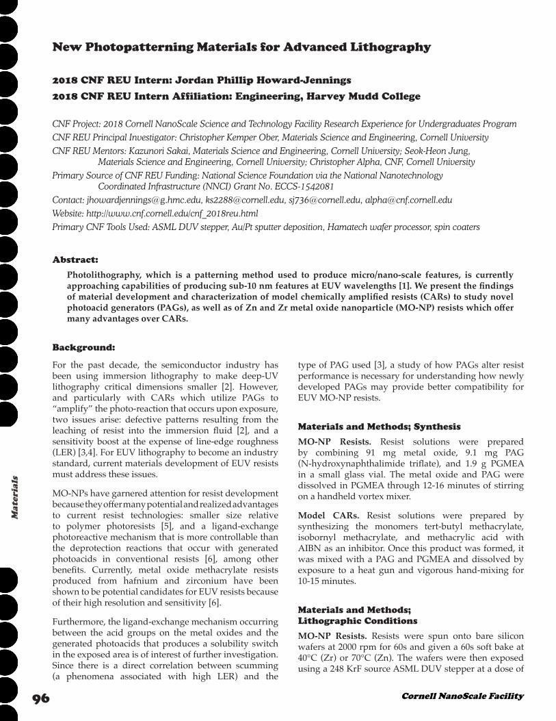
MO-NP Resists. Current resist development demon-strates that while good feature production is possible (Figure 1), randomly dispersed particle defects (Figure 2) and incomplete pattern registering (Figure 3) significantly distort these features. The cause of these defects is not currently understood. For the Zn-oxide resist evaluated, the gradient-matching between the particle defects and the exposed/non-developed regions (lighter area) suggest that there could be issues in material preparation such as mixing of components.
Model CARs. While the appearance of desired patterns offers confirmation that the lithography happened, the model CARs run into two issues: First, randomly
dispersed porous defects dominate both the exposed and non-exposed areas, strongly suggesting that further materials development is needed. Second, the small gradient change between the patterned and non-patterned regions suggests that the height of the patterns is negligible (this observation is confirmed by the optical profilometer), suggesting that lithographic conditions used were not optimal.
Future Work:
Further materials development in conjunction with lithographic parameter optimization is necessary to reduce the preliminary defects observed in both the MO-NP resists and the model CARs. After these defects are eliminated, an expansive design-of-experiments may be implemented to evaluate factor interactions between different material properties (i.e., PAG type/amount, metal oxides, etc.) and lithographic conditions (i.e., spin times, bake times, exposure doses, etc.).
Acknowledgements:
This work was performed in part at the Cornell NanoScale Facility, a member of the National Nanotechnology Coordinated Infrastructure (NNCI), which is supported by the NSF (Grant ECCS-1542081).
References:[1] Li, Li, et al. Chemical Society Reviews. doi: 10.1039/C7CS00080D
(2017).
[2] Petrillo, Karen, et al. Advances in Resist Technology and Processing XXII. doi: 10.1117/12.601621(2005).
[3] Kosma, Vasiliki, et al. “Extreme Ultraviolet (EUV) Lithography IX. doi: 10.1117/12.2297383 (2018).
[4] Thiyagarajan, Muthiah, Kim Dean, and Kenneth E. Consalves. Journal of Photopolymer Science and Technology. doi: 10.2494/photopolymer.18.737 (2005).
[5] Krysak, Marie, et al. Advances in Resist Materials and Processing Technology XXVIII. doi: 10.1117/12.879385 (2011).
[6] Jiang, Jing, et al. Journal of Photopolymer Science and Technology. doi: 10.2494/photopolymer.27.663 (2014).
Figure 1: SEM image of various width patterns (largest 1000 nm) of Zn-oxide NP resists. Figure 2: SEM image of a 1000 nm-width pattern from the Zn-oxide NP resist. Figure 3: SEM image of a 500 nm-width pattern (center) from the Zr-oxide NP resist. Figure 4: SEM image of a pattern exposed region from the CARs.

98 Cornell NanoScale Facility
Mat
eria
ls
Electrical Characterization of In2Ga2ZnO7 Crystallized by Millisecond Heating
CNF Project Number: 150-82
Principal Investigator: Michael O. Thompson
User: Katherine K. Quinn
Affiliation: Materials Science and Engineering, Cornell UniversityPrimary Source of Research Funding: Air Force Office of Scientific Research (AFOSR)Contact: [email protected], [email protected]: http://thompson.mse.cornell.edu/Primary CNF Tools Used: Furnace B2, Oxford 100 PECVD, Plasma-Therm 720, CHA evaporator, SÜSS MicroTech MA6
Abstract:
In this work, we examined the electrical properties of In2Ga2ZnO7 films crystallized by laser spike annealing (LSA) for a dwell time of 10 ms. Using the lateral gradient LSA method, samples were annealed and crystallization was visibly observed. Spatially resolved sheet resistance measurements were attempted across the LSA stripe using patterned van der Pauw structures. Films as annealed were insulating with a conductance below 10-8 S and exhibited only capacitor-like behavior. Analysis suggests that a thin SiO2 passivation layer remained on films during processing leading to the observed behavior.
Summary of Research:
Over the past two decades, various amorphous oxide semiconductors have been explored as alternatives to amorphous hydrogenated silicon used in thin film transistors for large area displays. The In2O3-Ga2O3-ZnO (IGZO) material system in particular exhibits promising electrical characteristics including high electron mobility and stable carrier concentration. However, devices fabricated with amorphous IGZO (a-IGZO) are limited by turn-on voltage instabilities. While crystalline forms of IGZO maintain favorable electrical characteristics and do not exhibit device instabilities like a-IGZO, only films formed during heated substrate depositions have been studied. Alternatively, it is possible to crystallize a-IGZO films on short time scales (250 µs to 10 ms) using laser spike annealing techniques, however, very little is known about the electronic properties of metastable crystallized alloys in the IGZO system.
Van der Pauw devices were fabricated on lightly doped p-type Si wafers with ~ 80 nm of thermally grown SiO2 for the purposes of electrical characterization (Furnace B2). Amorphous thin film samples of In2Ga2ZnO7 were deposited onto rotating substrates using a reactive RF magnetron sputtering system in a 10% O2 in Ar mix with 120 W power. An ~ 30 nm thick passivating layer of SiO2 was deposited to protect the IGZO surface (Oxford 100 plasma-enhanced vapor deposition). Samples were photolithographically patterned to form van der Pauw structure arrays, as shown in Figure 1 (SÜSS MicroTech
Figure 1: Schematic of van der Pauw device subarray consisting of 11 rows containing seven devices each. Above each subarray are alignment marks used to align the beam center during LSA. Inset is approximate scale of one device stripe on a 2 cm × 2 cm sample.
MA6). The SiO2 passivation layer was patterned using fluorine-based dry etching (Plasma-Therm 720) and IGZO was patterned using 2 wt.% HCl wet etching. After patterning, samples were annealed at 350°C with 7 sccm N2 for 30 min in a quartz tube furnace.

992017-2018 Research Accomplishments
Materials
Lateral gradient LSA (lgLSA) was used to crystallize the films. LSA uses a line-focused continuous wave laser beam to scan across a sample for controlled time durations (dwell). In lgLSA, the beam is intentionally non-uniform orthogonal to the scanning direction to produce a lateral temperature profile across the device row, allowing for electrical characterization as a function of peak annealing temperature.
This implied that a material in the device stack was non-conducting and contributing to the measured device capacitance. The SiO2 passivation layer, the active IGZO layer, and the thermally-grown SiO2 layer on the Si substrate were considered as possible sources of the capacitance. After comparing the estimated layer thickness of each material to a calculated thickness required to yield a 96 pF capacitance, it was found that only a thin remainder of the passivation SiO2 layer could be responsible for the capacitance. The most probable explanation for this observed capacitance is that the SiO2 passivation layer was not completely etched during processing of the van der Pauw devices, resulting in a dielectric layer between the IGZO and the metal contacts. This motivates future improvements in the etching techniques used in the fabrication of devices.
References:[1] Kamiya, Toshio and Hosono, Hideo. (2010). “Material
characteristics and applications of transparent amorphous oxide semiconductors.” NPG Asia Materials. 2, pp. 15-22. DOI: 10.1038/asiamat.2010.5.
[2] Lynch, David. (2017). “Indium Gallium Zinc Oxide: phase formation and crystallization kinetics during millisecond laser spike annealing.” (Doctoral dissertation).
[3] Yamazaki, Shunpei. (2013). “A possibility of crystalline Indium-Gallium-Zinc-Oxide,” Fifth Asia Symposium on Quality Electronic Design (ASQED 2013), pp. 1-5. DOI: 10.1109/ASQED.2013.6643553.
[4] Chung, Chen-Yang. (2016). “High mobility of sputtered In2Ga2ZnO7 (IGZO) thin film transistors (TFTs).” (Doctoral dissertation).
[5] Bell, Robert. (2016). “Lateral Temperature-Gradient Method for High-Throughput Characterization of Material Processing by Millisecond Laser Annealing.” ACS Combinatorial Science. 18, pp. 548.558. DOI: 10.1021/acscombsci.6b00043.
Figure 3: 4-point van der Pauw resistance measurements at 10 nA exhibited a parabolic IV curve, indicating the charging and discharging of current that is characteristic to capacitor behavior.
Figure 2: Evident structural transition indicated by color change along row of devices resulting from anneal by diode laser at 70.9 A for 10 ms dwell.
Samples were irradiated with fiber-coupled diode laser (980 nm wavelength, 1.5 mm full width half maximum) for 10 ms dwells, achieving expected anneal peak temperatures above and below a known Si melt temperature of 1414°C. Figure 2 shows a photomicro-graph of an anneal stripe that produced a dark to light color gradient across the device rows, confirming a structural transition from an amorphous structure to the crystalline phase within the lateral temperature gradient.
Metal contacts were deposited (CHA Evaporator) and patterned using liftoff. Electrical measurements of devices were conducted using a 4-point manual probe station and a Keithley 2400 Source Measurement Unit (SMU) to supply current and measure voltage. Contact resistance and 4-point van der Pauw resistance measurements were obtained.
Initial resistance measurements ranged in the 60-200 MΩ range, indicating essentially non-conducting films. In contrast to the expected linear behavior of a conductive material, the IV characteristics showed parabolic curvature as seen in the resistance scans in Figure 3. This behavior is consistent with the material acting as a capacitor in that the material charges to a voltage at the application of negative current, then begins discharging symmetrically when the direction of current is reversed. The capacitance of the van der Pauw devices was extracted and found to be 96 pF.
100 Cornell NanoScale Facility
Mat
eria
ls
Fused Silica Substrate and Silicon Absorber Film for use in Laser Spike Annealing (LSA)
CNF Project Number: 150-82
Principal Investigator: Michael O. Thompson
Users: Juliane M. Scholtz, Yi (Johnny) Zhang
Affiliations: Department of Physics, Department of Materials Science and Engineering; Cornell UniversityPrimary Source of Research Funding: Department of Defense through a
Multidisciplinary University Research Initiative (MURI)Contact: [email protected], [email protected], [email protected] CNF Tools Used: Oxford 100 PECVD, Nikon Eclipse L200N optical microscope, Tencor P10 profilometer
Abstract:
Laser spike annealing (LSA), performed at various dwell times and generating various peak temperatures [1], is used to induce metastable phases in a variety of materials. An alternate LSA setup, which would allow annealing of metals and transparent dielectrics, requires the appropriate choice of a substrate, which is annealed directly, and an absorber film, which conducts heat to the material of interest. We investigate fused silica and silicon as candidates for substrate and absorber film, respectively. An Si thin-film was deposited via plasma enhanced chemical vapor deposition (PECVD) on a fused silica substrate and subjected to LSA with a CO2 laser (10.6 µm) at various powers. LSA was performed on the glass substrate with a laser diode (980 nm) at various currents and dwell times. Profilometer measurements of the CO2 anneals suggest Si ablation and potential substrate damage at 20.55W, as well as lesser ablation or an increase in grain size at lower powers. Laser diode annealing of the fused silica substrate caused no damage visible to the eye. Our work contributes to the development of a “universal substrate” for use in the modified laser spike annealing setup.
Summary of Research:
Laser spike annealing (LSA), performed at various dwell times and peak temperatures [1], is used to induce metastable phases in a variety of systems, such as Bi2O3 and MnTiO3 [2]. To allow annealing of additional materials, including transparent dielectrics and metals, an alternate LSA method is in development. Annealing is performed from the substrate side of the sample, allowing an absorber film to conduct the heat to the material under investigation. Appropriate substrate and film choices will therefore withstand anneals that induce a wide range of peak temperatures and occur at different dwell times. Previous research has revealed inadequacies of sapphire substrates for LSA [3]. In this project, silicon (Si) and fused silica were investigated as potential absorber film and substrate, respectively. As peak temperature calibrations for these materials have yet to be performed using our laser setup, we explored the behavior of our substrate and film at varying laser power (or current) and dwell time.
A 100 mm diameter, 500 µm-thick fused silica wafer, polished on both sides, was purchased from the Cornell NanoScale Science and Technology Facility (CNF) and
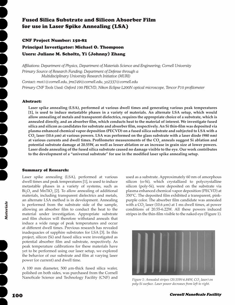
used as a substrate. Approximately 60 nm of amorphous silicon (a-Si), which crystallized to polycrystalline silicon (poly-Si), were deposited on the substrate via plasma enhanced chemical vapor deposition (PECVD) at 350°C. The deposited film exhibited a transparent, pink-purple color. The absorber film candidate was annealed with a CO2 laser (10.6 µm) at 1 ms dwell times, at power conditions of 20.55-6.22W. All these powers induced stripes in the thin-film visible to the naked eye (Figure 1).
Figure 1: Annealed stripes (20.55W-6.84W, CO2 laser) on poly-Si surface. Laser power decreases from left to right.

1012017-2018 Research Accomplishments
Materials
Stripes annealed at powers of 20.55W-10.8W appeared clear, while the film annealed at lower powers displayed a color change to light green.
To understand the physical changes that occurred in the sample during annealing, step heights between the annealed stripe centers and the surrounding thin-film were investigated using a Tencor P10 Profilometer. Stripes annealed at powers of 20.55W and 18.43W, respectively, which appeared clear to the naked eye, evidenced film ablation under profilometer examination. A step height of 1.097 µm (1097 nm) in the former stripe suggests both complete ablation of the 60 nm film and CO2 laser damage to the glass substrate beneath. This conjecture is supported by an additional set of anneals, in which CO2 laser annealing at 20.55W directly onto the fused silica produced a damage stripe (Figure 2). The second annealed stripe (18.432W) evidenced 425Å (42.5 nm) between stripe center and unannealed film. This indicates a relatively complete ablation of the thin-film by the CO2 laser.
To further examine fused silica’s potential as an LSA substrate, the glass was directly subjected to laser spike annealing with a laser diode (wavelength 980 nm). A set of five anneals (5 ms dwell times), with currents increasing from 63.58 Amps to 100.22 Amps, caused no damage to the substrate visible to the naked eye. To perform subsequent anneals at 100 Amps or below, the dwell time was increased. Two anneals, performed at 87.68 Amps and 97.76 Amps, respectively, with dwell time 10 ms, also caused no visible damage to the glass substrate. A further two anneals at 20 ms dwell times and currents of 82.5 Amps and 85.99 Amps, respectively, produced the same result.
We have studied the behavior of fused silica substrates and silicon absorber films under CO2 and laser diode laser spike annealing. The absence of visible laser-induced damage from the laser diode suggests fused silica is a promising substrate for laser diode LSA. However, this substrate is susceptible to damage from CO2 lasers, even at relatively low powers. PECVD deposition of a-Si should be performed at the standard 200°C, to prevent premature crystallization and allow for a true study of amorphous silicon as a potential absorber film. Our work contributes to the development of a “universal substrate” for use in the modified laser spike annealing setup.
References:[1] R. Bell, et al. ACS Comb. Sci. 18, 548 (2016).
[2] R. Bell, Ph.D. thesis, Cornell University (2017).
[3] H.-L. Huang, et al. Cornell NanoScale Science and Technology Facility Report, http://www.cnf.cornell.edu/doc/2017cnfRA/2017cnfRA_222.pdf (2017).
Figure 3: P10 Profilometer measurement of LSA stripe (10.267W, CO2 laser) on silicon thin-film. Scale: vertical axis: x100Å, horizontal axis: µm.
Figure 2: Dark-field view of LSA stripe (20.55W, CO2 laser) on a fused silica substrate.
Two of the green-colored stripes were also examined with the profilometer. Both the fifth (10.267W) and sixth (9.724W) stripe measurements displayed large amounts of noise in their respective annealed regions. As a result, the Ra (roughness average) was parameter of importance. The fifth stripe had an Ra of 198Å, while the sixth evidenced an Ra of 156.4Å. Thus, a lower roughness average is observed at lower laser power. Noise observed in the profilometer measurements of the stripes may indicate that the poly-Si has transformed from small-grain to large-grain during the annealing process (Figure 3).
102 Cornell NanoScale Facility
Mat
eria
ls
Metal-Organic Complex Photoresists
CNF Project Number: 386-90
Principal Investigator: Christopher Kemper Ober
Users: Kazunori Sakai, Hong Xu, Vasiliki Kosma
Affiliation: Materials Science and Engineering, Cornell UniversityPrimary Source of Research Funding: JSR CorporationContact: [email protected], [email protected], [email protected], [email protected] CNF Tools Used: Zeiss Supra SEM, ASML 300C DUV Stepper, ABM Contact Aligner
Abstract:
The most advanced microelectronics are made by using 193 nm immersion lithography systems, but it is difficult to follow the rapid development of semiconductors due to approaching its physical limits. Extreme ultraviolet (EUV) lithography, which use shorter wavelength (i.e., 13.5 nm), can offer the way to print under 40 nm lines and spaces. EUV lithography requires photoresist to utilize EUV photons because photons generated by EUV exposure are fewer than photons generated by 193 nm light exposure. One of the approaching for utilizing fewer EUV photons is using higher EUV absorption elements such as transition metals. We have continuously developed metal-oxide nanoparticles resists since we reported our first example of hafnium oxide nanoparticle resist [1]. In this report, our recent progress in metal oxide nanoparticle photoresist research will be described.
Figure 1: ESI-MS and SEM images after development of different metal oxide photoresists.
Summary of Research:
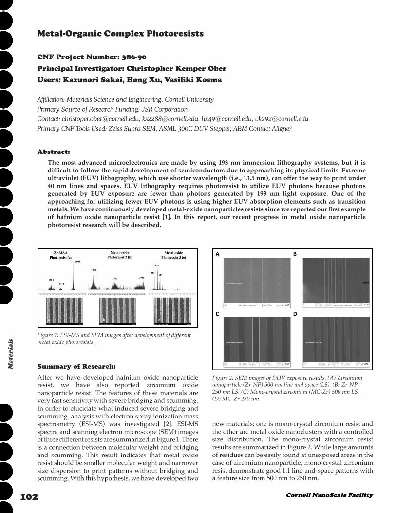
After we have developed hafnium oxide nanoparticle resist, we have also reported zirconium oxide nanoparticle resist. The features of these materials are very fast sensitivity with severe bridging and scumming. In order to elucidate what induced severe bridging and scumming, analysis with electron spray ionization mass spectrometry (ESI-MS) was investigated [2]. ESI-MS spectra and scanning electron microscope (SEM) images of three different resists are summarized in Figure 1. There is a connection between molecular weight and bridging and scumming. This result indicates that metal oxide resist should be smaller molecular weight and narrower size dispersion to print patterns without bridging and scumming. With this hypothesis, we have developed two
new materials; one is mono-crystal zirconium resist and the other are metal oxide nanoclusters with a controlled size distribution. The mono-crystal zirconium resist results are summarized in Figure 2. While large amounts of residues can be easily found at unexposed areas in the case of zirconium nanoparticle, mono-crystal zirconium resist demonstrate good 1:1 line-and-space patterns with a feature size from 500 nm to 250 nm.
Figure 2: SEM images of DUV exposure results. (A) Zirconium nanoparticle (Zr-NP) 500 nm line-and-space (LS). (B) Zr-NP 250 nm LS. (C) Mono-crystal zirconium (MC-Zr) 500 nm LS. (D) MC-Zr 250 nm.
1032017-2018 Research Accomplishments
Materials
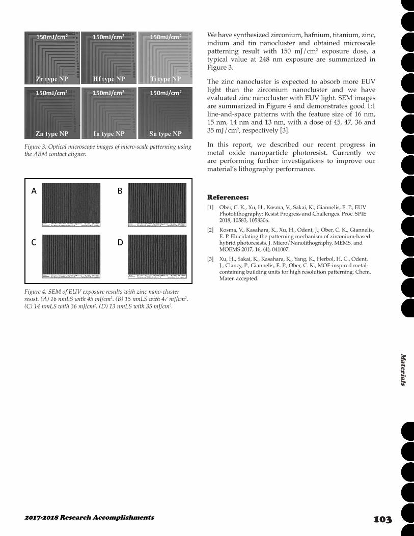
We have synthesized zirconium, hafnium, titanium, zinc, indium and tin nanocluster and obtained microscale patterning result with 150 mJ/cm2 exposure dose, a typical value at 248 nm exposure are summarized in Figure 3.
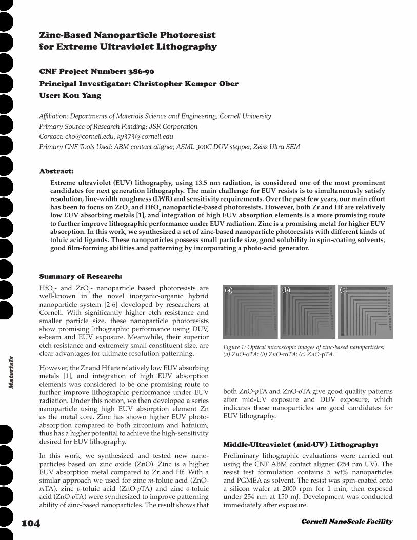
The zinc nanocluster is expected to absorb more EUV light than the zirconium nanocluster and we have evaluated zinc nanocluster with EUV light. SEM images are summarized in Figure 4 and demonstrates good 1:1 line-and-space patterns with the feature size of 16 nm, 15 nm, 14 nm and 13 nm, with a dose of 45, 47, 36 and 35 mJ/cm2, respectively [3].
In this report, we described our recent progress in metal oxide nanoparticle photoresist. Currently we are performing further investigations to improve our material’s lithography performance.
References:[1] Ober, C. K., Xu, H., Kosma, V., Sakai, K., Giannelis, E. P., EUV
Photolithography: Resist Progress and Challenges. Proc. SPIE 2018, 10583, 1058306.
[2] Kosma, V., Kasahara, K., Xu, H., Odent, J., Ober, C. K., Giannelis, E. P. Elucidating the patterning mechanism of zirconium-based hybrid photoresists. J. Micro/Nanolithography, MEMS, and MOEMS 2017, 16, (4), 041007.
[3] Xu, H., Sakai, K., Kasahara, K., Yang, K., Herbol, H. C., Odent, J., Clancy, P., Giannelis, E. P., Ober, C. K., MOF-inspired metal-containing building units for high resolution patterning, Chem. Mater. accepted.
Figure 4: SEM of EUV exposure results with zinc nano-cluster resist. (A) 16 nmLS with 45 mJ/cm2. (B) 15 nmLS with 47 mJ/cm2. (C) 14 nmLS with 36 mJ/cm2. (D) 13 nmLS with 35 mJ/cm2.
Figure 3: Optical microscope images of micro-scale patterning using the ABM contact aligner.
104 Cornell NanoScale Facility
Mat
eria
ls
Zinc-Based Nanoparticle Photoresist for Extreme Ultraviolet Lithography
CNF Project Number: 386-90
Principal Investigator: Christopher Kemper Ober
User: Kou Yang
Affiliation: Departments of Materials Science and Engineering, Cornell UniversityPrimary Source of Research Funding: JSR CorporationContact: [email protected], [email protected] CNF Tools Used: ABM contact aligner, ASML 300C DUV stepper, Zeiss Ultra SEM
Abstract:
Extreme ultraviolet (EUV) lithography, using 13.5 nm radiation, is considered one of the most prominent candidates for next generation lithography. The main challenge for EUV resists is to simultaneously satisfy resolution, line-width roughness (LWR) and sensitivity requirements. Over the past few years, our main effort has been to focus on ZrO2 and HfO2 nanoparticle-based photoresists. However, both Zr and Hf are relatively low EUV absorbing metals [1], and integration of high EUV absorption elements is a more promising route to further improve lithographic performance under EUV radiation. Zinc is a promising metal for higher EUV absorption. In this work, we synthesized a set of zinc-based nanoparticle photoresists with different kinds of toluic acid ligands. These nanoparticles possess small particle size, good solubility in spin-coating solvents, good film-forming abilities and patterning by incorporating a photo-acid generator.
Summary of Research:
HfO2- and ZrO2- nanoparticle based photoresists are well-known in the novel inorganic-organic hybrid nanoparticle system [2-6] developed by researchers at Cornell. With significantly higher etch resistance and smaller particle size, these nanoparticle photoresists show promising lithographic performance using DUV, e-beam and EUV exposure. Meanwhile, their superior etch resistance and extremely small constituent size, are clear advantages for ultimate resolution patterning.
However, the Zr and Hf are relatively low EUV absorbing metals [1], and integration of high EUV absorption elements was considered to be one promising route to further improve lithographic performance under EUV radiation. Under this notion, we then developed a series nanoparticle using high EUV absorption element Zn as the metal core. Zinc has shown higher EUV photo-absorption compared to both zirconium and hafnium, thus has a higher potential to achieve the high-sensitivity desired for EUV lithography.
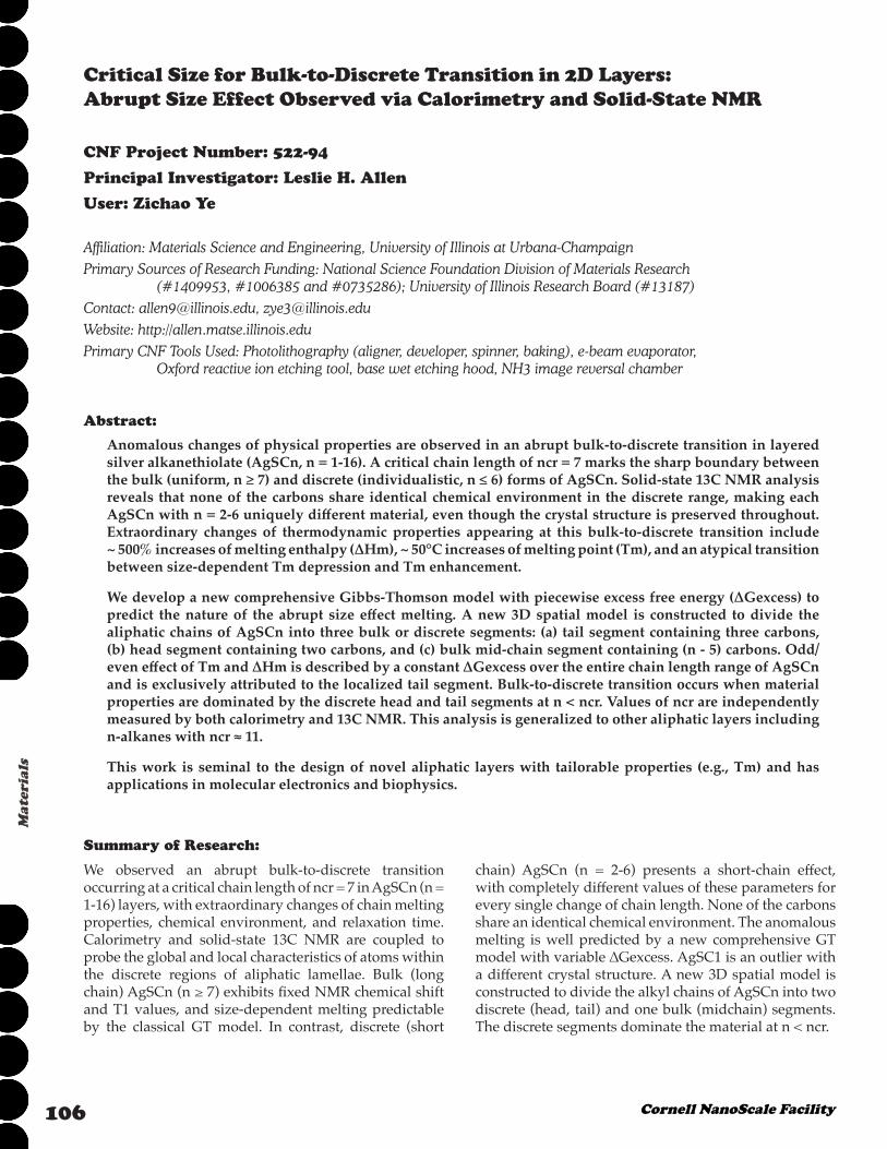
In this work, we synthesized and tested new nano-particles based on zinc oxide (ZnO). Zinc is a higher EUV absorption metal compared to Zr and Hf. With a similar approach we used for zinc m-toluic acid (ZnO-mTA), zinc p-toluic acid (ZnO-pTA) and zinc o-toluic acid (ZnO-oTA) were synthesized to improve patterning ability of zinc-based nanoparticles. The result shows that
Figure 1: Optical microscopic images of zinc-based nanoparticles: (a) ZnO-oTA; (b) ZnO-mTA; (c) ZnO-pTA.
both ZnO-pTA and ZnO-oTA give good quality patterns after mid-UV exposure and DUV exposure, which indicates these nanoparticles are good candidates for EUV lithography.
Middle-Ultraviolet (mid-UV) Lithography:
Preliminary lithographic evaluations were carried out using the CNF ABM contact aligner (254 nm UV). The resist test formulation contains 5 wt% nanoparticles and PGMEA as solvent. The resist was spin-coated onto a silicon wafer at 2000 rpm for 1 min, then exposed under 254 nm at 150 mJ. Development was conducted immediately after exposure.

1052017-2018 Research Accomplishments
Materials
As shown in Figure 1, clear patterns can be obtained after mid-UV exposure. Pictures were taken by Nikon Microscope Cameras in CNF.
Deep Ultraviolet (DUV) Lithography:
With similar lithographic conditions in mid-UV exposure, the zinc-based nanoparticles are further exposed upon 248 deep-UV radiation using ASML 300C DUV Stepper in CNF. The film is exposed at 150 mJ/cm2 as normal condition and developed in acetone. Developing time varies by different nanoparticles. Well-defined 1:1 line-and-space patterns negative tone patterns with feature size from 1000 nm to 250 nm were obtained, as indicated by scanning electron microscope (SEM) images (Figure 2 to Figure 4), taken by CNF Zeiss Ultra SEM.
In summary, we developed new ligands for zinc-based nanoparticles used in extreme ultraviolet lithography. These zinc-oxide based nanoparticles possess good solubility in spin-coating solvents, good film-forming ability and moderate patterning performance under mid-UV and deep-UV radiations. Considering the high EUV photo-absorption of zinc metal, this preliminary
work indicates such zinc-based nanoparticles would be promising candidates for EUV lithography. Further structure analysis, patterning mechanism study and lithography tests including EUV lithography patterning tests are ongoing using these zinc-based nanoparticles.
References:[1] B. L. Henke et al., X-Ray Interactions: photoabsorption,
scattering, transmission, and reflection at E = 50~30,000 eV, Z = 1-92. At. Data Nucl. Data Tables, 54, 181-342 (1993).
[2] M. Trikeriotis, et al., Development of an inorganic photoresist for DUV, EUV, and electron beam imaging. Proc. SPIE 7639, 76390E (2010).
[3] W. J. Bae, et al., High refractive index and high transparency HfO2 nanocomposites for next generation lithography. J. Mater. Chem. 20, 5186-5189 (2010).
[4] M. Krysak, et al., Development of an inorganic nanoparticle photoresist for EUV, E-beam, and 193nm lithography. Proc. SPIE 7972, 79721C (2011).
[5] M. Trikeriotis, et al., A new inorganic EUV resist with high-etch resistance. Proc. SPIE 8322, 83220U (2012).
[6] S. Chakrabarty, et al., Increasing sensitivity of oxide nanoparticle photoresists. Proc. SPIE 9048, 90481C (2014).
Figure 4: SEM images of ZnO-pTA nanoparticles: (a) 250 nm; (b) 500 nm; (c) 1000 nm.
Figure 2: SEM images of ZnO-oTA nanoparticles: (a) 250 nm; (b) 500 nm; (c) 1000 nm.
Figure 3: SEM images of ZnO-mTA nanoparticles: (a) 250 nm; (b) 500 nm; (c) 1000 nm.
106 Cornell NanoScale Facility
Mat
eria
ls
Critical Size for Bulk-to-Discrete Transition in 2D Layers: Abrupt Size Effect Observed via Calorimetry and Solid-State NMR
CNF Project Number: 522-94
Principal Investigator: Leslie H. Allen
User: Zichao Ye
Affiliation: Materials Science and Engineering, University of Illinois at Urbana-ChampaignPrimary Sources of Research Funding: National Science Foundation Division of Materials Research
(#1409953, #1006385 and #0735286); University of Illinois Research Board (#13187)Contact: [email protected], [email protected]: http://allen.matse.illinois.eduPrimary CNF Tools Used: Photolithography (aligner, developer, spinner, baking), e-beam evaporator,
Oxford reactive ion etching tool, base wet etching hood, NH3 image reversal chamber
Abstract:
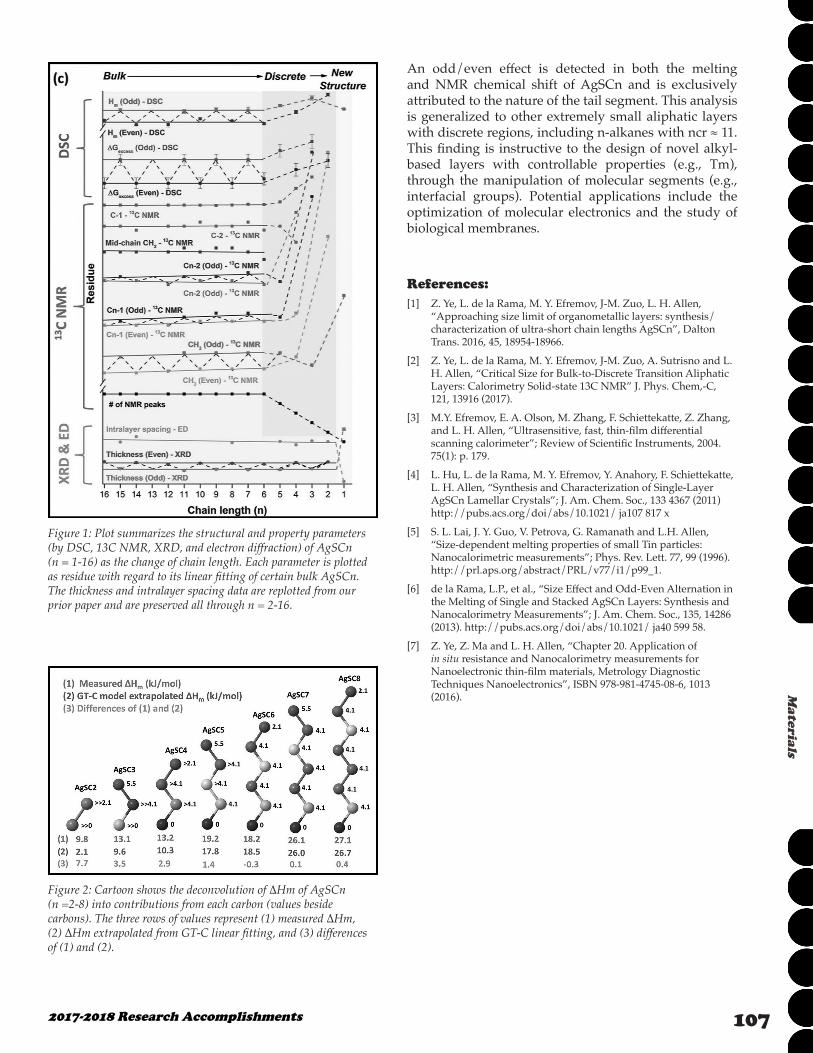
Anomalous changes of physical properties are observed in an abrupt bulk-to-discrete transition in layered silver alkanethiolate (AgSCn, n = 1-16). A critical chain length of ncr = 7 marks the sharp boundary between the bulk (uniform, n ≥ 7) and discrete (individualistic, n ≤ 6) forms of AgSCn. Solid-state 13C NMR analysis reveals that none of the carbons share identical chemical environment in the discrete range, making each AgSCn with n = 2-6 uniquely different material, even though the crystal structure is preserved throughout. Extraordinary changes of thermodynamic properties appearing at this bulk-to-discrete transition include ~ 500% increases of melting enthalpy (∆Hm), ~ 50°C increases of melting point (Tm), and an atypical transition between size-dependent Tm depression and Tm enhancement.
We develop a new comprehensive Gibbs-Thomson model with piecewise excess free energy (∆Gexcess) to predict the nature of the abrupt size effect melting. A new 3D spatial model is constructed to divide the aliphatic chains of AgSCn into three bulk or discrete segments: (a) tail segment containing three carbons, (b) head segment containing two carbons, and (c) bulk mid-chain segment containing (n - 5) carbons. Odd/even effect of Tm and ∆Hm is described by a constant ∆Gexcess over the entire chain length range of AgSCn and is exclusively attributed to the localized tail segment. Bulk-to-discrete transition occurs when material properties are dominated by the discrete head and tail segments at n < ncr. Values of ncr are independently measured by both calorimetry and 13C NMR. This analysis is generalized to other aliphatic layers including n-alkanes with ncr ≈ 11.
This work is seminal to the design of novel aliphatic layers with tailorable properties (e.g., Tm) and has applications in molecular electronics and biophysics.
Summary of Research:
We observed an abrupt bulk-to-discrete transition occurring at a critical chain length of ncr = 7 in AgSCn (n = 1-16) layers, with extraordinary changes of chain melting properties, chemical environment, and relaxation time. Calorimetry and solid-state 13C NMR are coupled to probe the global and local characteristics of atoms within the discrete regions of aliphatic lamellae. Bulk (long chain) AgSCn (n ≥ 7) exhibits fixed NMR chemical shift and T1 values, and size-dependent melting predictable by the classical GT model. In contrast, discrete (short
chain) AgSCn (n = 2-6) presents a short-chain effect, with completely different values of these parameters for every single change of chain length. None of the carbons share an identical chemical environment. The anomalous melting is well predicted by a new comprehensive GT model with variable ∆Gexcess. AgSC1 is an outlier with a different crystal structure. A new 3D spatial model is constructed to divide the alkyl chains of AgSCn into two discrete (head, tail) and one bulk (midchain) segments. The discrete segments dominate the material at n < ncr.
1072017-2018 Research Accomplishments
Materials
An odd/even effect is detected in both the melting and NMR chemical shift of AgSCn and is exclusively attributed to the nature of the tail segment. This analysis is generalized to other extremely small aliphatic layers with discrete regions, including n-alkanes with ncr ≈ 11. This finding is instructive to the design of novel alkyl-based layers with controllable properties (e.g., Tm), through the manipulation of molecular segments (e.g., interfacial groups). Potential applications include the optimization of molecular electronics and the study of biological membranes.
References:[1] Z. Ye, L. de la Rama, M. Y. Efremov, J-M. Zuo, L. H. Allen,
“Approaching size limit of organometallic layers: synthesis/characterization of ultra-short chain lengths AgSCn”, Dalton Trans. 2016, 45, 18954-18966.
[2] Z. Ye, L. de la Rama, M. Y. Efremov, J-M. Zuo, A. Sutrisno and L. H. Allen, “Critical Size for Bulk-to-Discrete Transition Aliphatic Layers: Calorimetry Solid-state 13C NMR” J. Phys. Chem,-C, 121, 13916 (2017).
[3] M.Y. Efremov, E. A. Olson, M. Zhang, F. Schiettekatte, Z. Zhang, and L. H. Allen, “Ultrasensitive, fast, thin-film differential scanning calorimeter”; Review of Scientific Instruments, 2004. 75(1): p. 179.
[4] L. Hu, L. de la Rama, M. Y. Efremov, Y. Anahory, F. Schiettekatte, L. H. Allen, “Synthesis and Characterization of Single-Layer AgSCn Lamellar Crystals”; J. Am. Chem. Soc., 133 4367 (2011) http://pubs.acs.org/doi/abs/10.1021/ ja107 817 x
[5] S. L. Lai, J. Y. Guo, V. Petrova, G. Ramanath and L.H. Allen, “Size-dependent melting properties of small Tin particles: Nanocalorimetric measurements”; Phys. Rev. Lett. 77, 99 (1996). http://prl.aps.org/abstract/PRL/v77/i1/p99_1.
[6] de la Rama, L.P., et al., “Size Effect and Odd-Even Alternation in the Melting of Single and Stacked AgSCn Layers: Synthesis and Nanocalorimetry Measurements”; J. Am. Chem. Soc., 135, 14286 (2013). http://pubs.acs.org/doi/abs/10.1021/ ja40 599 58.
[7] Z. Ye, Z. Ma and L. H. Allen, “Chapter 20. Application of in situ resistance and Nanocalorimetry measurements for Nanoelectronic thin-film materials, Metrology Diagnostic Techniques Nanoelectronics”, ISBN 978-981-4745-08-6, 1013 (2016).
Figure 2: Cartoon shows the deconvolution of ∆Hm of AgSCn (n =2-8) into contributions from each carbon (values beside carbons). The three rows of values represent (1) measured ∆Hm, (2) ∆Hm extrapolated from GT-C linear fitting, and (3) differences of (1) and (2).
Figure 1: Plot summarizes the structural and property parameters (by DSC, 13C NMR, XRD, and electron diffraction) of AgSCn (n = 1-16) as the change of chain length. Each parameter is plotted as residue with regard to its linear fitting of certain bulk AgSCn. The thickness and intralayer spacing data are replotted from our prior paper and are preserved all through n = 2-16.
108 Cornell NanoScale Facility
Mat
eria
ls
Manipulating and Controlling Graphene Adhesion
CNF Project Number: 900-00
Principal Investigators: William R. Dichtel1, Paul L. McEuen2
User: Chao Sun1
Affiliation(s): 1. Department of Chemistry and Chemical Biology, 2. Department of Physics; Cornell UniversityPrimary Source of Research Funding: National Science Foundation grant DMR-1120296Contact: [email protected], [email protected], [email protected] CNF Tools Used: E-beam evaporator, Oxford atomic layer deposition
Abstract:
We present a technique for patterning, measuring, and tuning surface energies between atomic layered materials and substrates under water. It is simple to implement, provides versatile, high precision measurements, and enables the development and engineering of adhesives at the nano scale. We use this technique to characterize the use of molecular pyrenes bound on glass, and optimize the pyrene density for maximum adhesion. Surface energy control immediately enables a graphene-transfer protocol that is resilient to adhesion failure under sonication. We further study the reproducibility and the hysteresis of adhesion and find a dramatic difference between peeling and re-adhesion that are insensitive to their timescales. More generally, our technique opens the door to a more complete and systematic approach to engineering stimuli-responsive adhesives and mechanical technologies at the nanoscale.
Summary of Research:
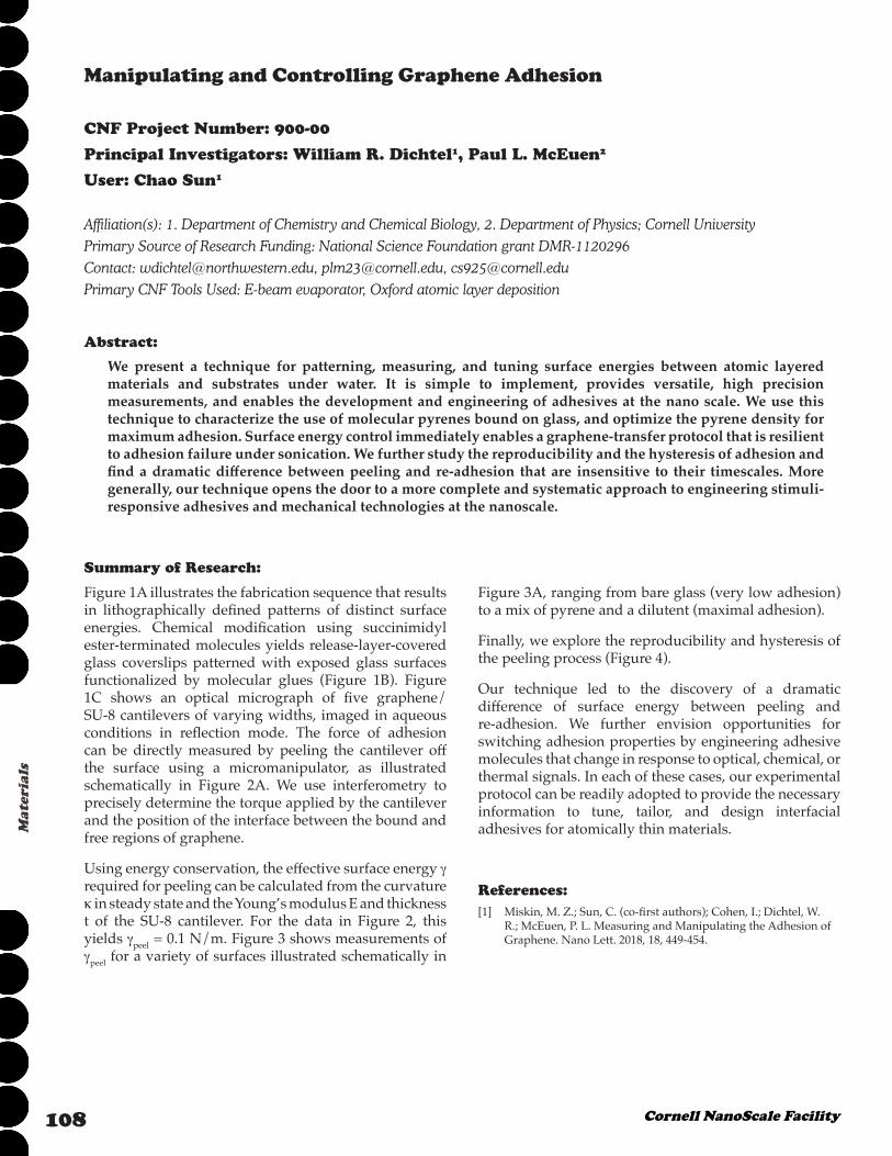
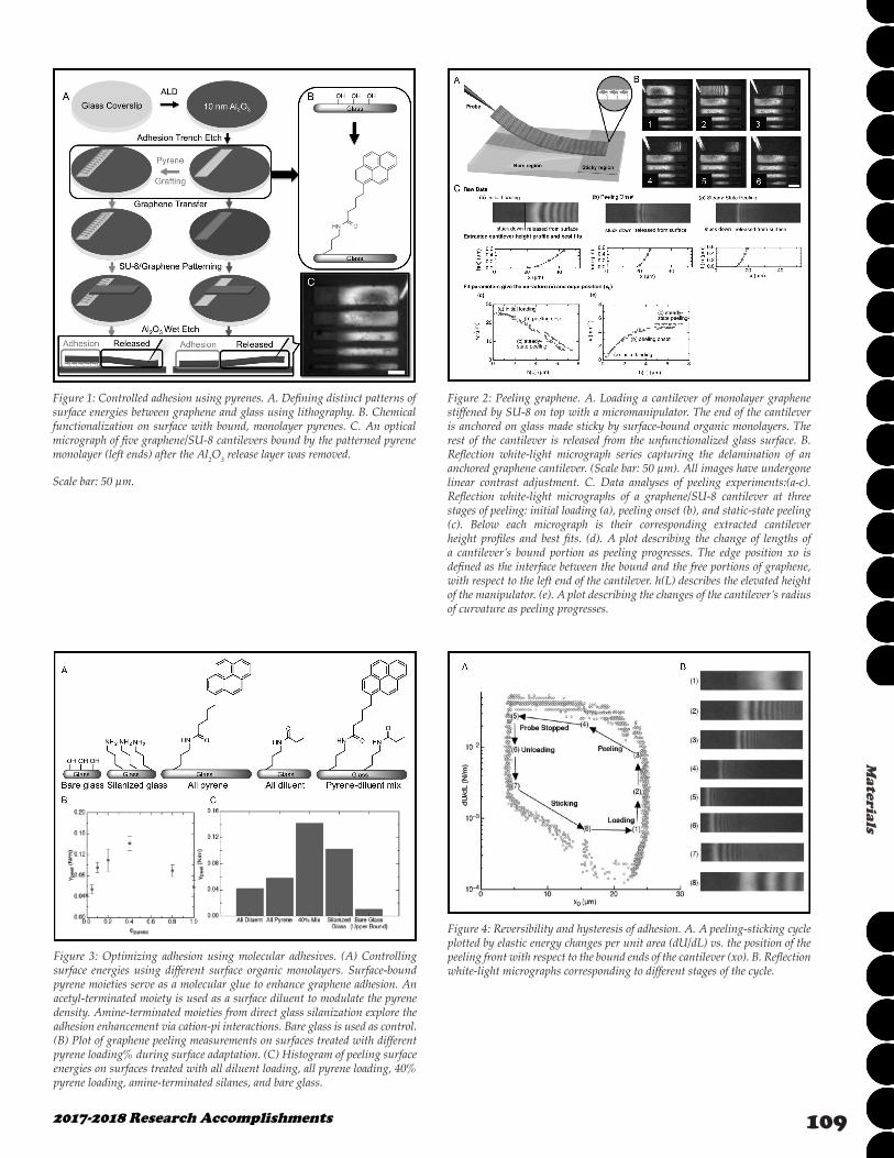
Figure 1A illustrates the fabrication sequence that results in lithographically defined patterns of distinct surface energies. Chemical modification using succinimidyl ester-terminated molecules yields release-layer-covered glass coverslips patterned with exposed glass surfaces functionalized by molecular glues (Figure 1B). Figure 1C shows an optical micrograph of five graphene/SU-8 cantilevers of varying widths, imaged in aqueous conditions in reflection mode. The force of adhesion can be directly measured by peeling the cantilever off the surface using a micromanipulator, as illustrated schematically in Figure 2A. We use interferometry to precisely determine the torque applied by the cantilever and the position of the interface between the bound and free regions of graphene.
Using energy conservation, the effective surface energy γ required for peeling can be calculated from the curvature k in steady state and the Young’s modulus E and thickness t of the SU-8 cantilever. For the data in Figure 2, this yields γpeel = 0.1 N/m. Figure 3 shows measurements of γpeel for a variety of surfaces illustrated schematically in
Figure 3A, ranging from bare glass (very low adhesion) to a mix of pyrene and a dilutent (maximal adhesion).
Finally, we explore the reproducibility and hysteresis of the peeling process (Figure 4).
Our technique led to the discovery of a dramatic difference of surface energy between peeling and re-adhesion. We further envision opportunities for switching adhesion properties by engineering adhesive molecules that change in response to optical, chemical, or thermal signals. In each of these cases, our experimental protocol can be readily adopted to provide the necessary information to tune, tailor, and design interfacial adhesives for atomically thin materials.
References:[1] Miskin, M. Z.; Sun, C. (co-first authors); Cohen, I.; Dichtel, W.
R.; McEuen, P. L. Measuring and Manipulating the Adhesion of Graphene. Nano Lett. 2018, 18, 449-454.
1092017-2018 Research Accomplishments
Materials
Figure 4: Reversibility and hysteresis of adhesion. A. A peeling-sticking cycle plotted by elastic energy changes per unit area (dU/dL) vs. the position of the peeling front with respect to the bound ends of the cantilever (xo). B. Reflection white-light micrographs corresponding to different stages of the cycle.
Figure 1: Controlled adhesion using pyrenes. A. Defining distinct patterns of surface energies between graphene and glass using lithography. B. Chemical functionalization on surface with bound, monolayer pyrenes. C. An optical micrograph of five graphene/SU-8 cantilevers bound by the patterned pyrene monolayer (left ends) after the Al2O3 release layer was removed.
Scale bar: 50 µm.
Figure 2: Peeling graphene. A. Loading a cantilever of monolayer graphene stiffened by SU-8 on top with a micromanipulator. The end of the cantilever is anchored on glass made sticky by surface-bound organic monolayers. The rest of the cantilever is released from the unfunctionalized glass surface. B. Reflection white-light micrograph series capturing the delamination of an anchored graphene cantilever. (Scale bar: 50 µm). All images have undergone linear contrast adjustment. C. Data analyses of peeling experiments:(a-c). Reflection white-light micrographs of a graphene/SU-8 cantilever at three stages of peeling: initial loading (a), peeling onset (b), and static-state peeling (c). Below each micrograph is their corresponding extracted cantilever height profiles and best fits. (d). A plot describing the change of lengths of a cantilever’s bound portion as peeling progresses. The edge position xo is defined as the interface between the bound and the free portions of graphene, with respect to the left end of the cantilever. h(L) describes the elevated height of the manipulator. (e). A plot describing the changes of the cantilever’s radius of curvature as peeling progresses.
Figure 3: Optimizing adhesion using molecular adhesives. (A) Controlling surface energies using different surface organic monolayers. Surface-bound pyrene moieties serve as a molecular glue to enhance graphene adhesion. An acetyl-terminated moiety is used as a surface diluent to modulate the pyrene density. Amine-terminated moieties from direct glass silanization explore the adhesion enhancement via cation-pi interactions. Bare glass is used as control. (B) Plot of graphene peeling measurements on surfaces treated with different pyrene loading% during surface adaptation. (C) Histogram of peeling surface energies on surfaces treated with all diluent loading, all pyrene loading, 40% pyrene loading, amine-terminated silanes, and bare glass.

110 Cornell NanoScale Facility
Mat
eria
ls
Transient Laser Heating Derived Mesoporous Materials Directed by Gyroidal Templates from Block Copolymer Self-Assembly
CNF Project Number: 1356-05
Principal Investigator: Ulrich Wiesner
Users: Qi Zhang, Fei Yu
Affiliation: Department of Materials Science and Engineering, Cornell UniversityPrimary Source of Research Funding: National Science Foundation (DMR-1719875)Contact: [email protected], [email protected], [email protected]: http://wiesner.mse.cornell.edu/Primary CNF Tools Used: TFT N+/P+ polysilicon furnace – A4, Oxford 81 etcher
Abstract:
Gyroidal thin films were fabricated from co-assembly of poly(isoprene)-block-poly(styrene)-block-poly(ethylene oxide) (ISO) and resorcinol formaldehyde resols through solvent vapor annealing. Upon crosslinking the resols and carbonizing the thin films, mesoporous carbon templates were obtained. Low-pressure chemical vapor deposition (LPCVD) was utilized to deposit amorphous silicon into the templates, which melted and crystallized during pulsed excimer laser irradiation to achieve conformal backfilling of the templates. Finally, by removing the carbon template, we successfully prepared 3D continuous crystalline silicon with the inverse gyroidal nanostructure.
Summary of Research:
Templates enable the manufacturing of materials with intricate and complicated structures. Templates at the nanoscale allow for bottom-up fabrication of nanomaterials, which could find applications in catalysis or electronics. Block copolymer self-assembly offers pathways to complex nanostructured templates, which can be combined with laser annealing for pattern transfer to produce porous ordered nanomaterials after template removal.
We first prepared such nanoscale organic templates derived from block copolymer self-assembly. To this end, poly(isoprene)-block-poly(styrene)-block-poly(ethylene oxide) (PI-b-PS-b-PEO, or ISO) was synthesized via sequential anionic polymerization as described elsewhere [1]. The resorcinol formaldehyde resols are hydrogen bonded to the PEO block of the amphiphilic ISO terpolymer, which underwent ISO-directed co-assembly in solvent vapor annealing and formed what is known as cubic co-continuous gyroidal structures in the appropriate swelling ratio window [2]. After the resols were crosslinked and carbonized at high temperatures, mesoporous carbon thin-film templates with gyroidal nanostructures were prepared (Figure 1).
Figure 1: Scanning electron microscopy (SEM) plan view of the mesoporous gyroidal carbon template, derived from ISO-resols hybrid carbonized at 450°C.
1112017-2018 Research Accomplishments
Materials
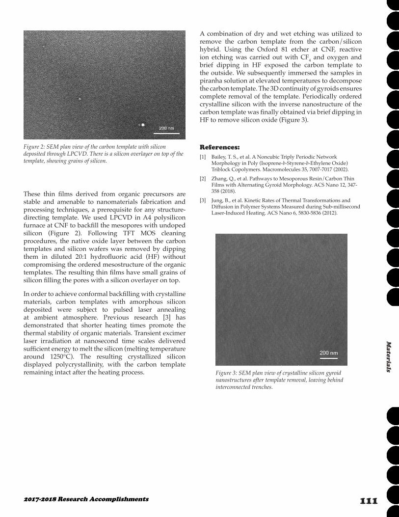
These thin films derived from organic precursors are stable and amenable to nanomaterials fabrication and processing techniques, a prerequisite for any structure-directing template. We used LPCVD in A4 polysilicon furnace at CNF to backfill the mesopores with undoped silicon (Figure 2). Following TFT MOS cleaning procedures, the native oxide layer between the carbon templates and silicon wafers was removed by dipping them in diluted 20:1 hydrofluoric acid (HF) without compromising the ordered mesostructure of the organic templates. The resulting thin films have small grains of silicon filling the pores with a silicon overlayer on top.
In order to achieve conformal backfilling with crystalline materials, carbon templates with amorphous silicon deposited were subject to pulsed laser annealing at ambient atmosphere. Previous research [3] has demonstrated that shorter heating times promote the thermal stability of organic materials. Transient excimer laser irradiation at nanosecond time scales delivered sufficient energy to melt the silicon (melting temperature around 1250°C). The resulting crystallized silicon displayed polycrystallinity, with the carbon template remaining intact after the heating process. Figure 3: SEM plan view of crystalline silicon gyroid
nanostructures after template removal, leaving behind interconnected trenches.
Figure 2: SEM plan view of the carbon template with silicon deposited through LPCVD. There is a silicon overlayer on top of the template, showing grains of silicon.
A combination of dry and wet etching was utilized to remove the carbon template from the carbon/silicon hybrid. Using the Oxford 81 etcher at CNF, reactive ion etching was carried out with CF4 and oxygen and brief dipping in HF exposed the carbon template to the outside. We subsequently immersed the samples in piranha solution at elevated temperatures to decompose the carbon template. The 3D continuity of gyroids ensures complete removal of the template. Periodically ordered crystalline silicon with the inverse nanostructure of the carbon template was finally obtained via brief dipping in HF to remove silicon oxide (Figure 3).
References:[1] Bailey, T. S., et al. A Noncubic Triply Periodic Network
Morphology in Poly (Isoprene-b-Styrene-b-Ethylene Oxide) Triblock Copolymers. Macromolecules 35, 7007-7017 (2002).
[2] Zhang, Q., et al. Pathways to Mesoporous Resin/Carbon Thin Films with Alternating Gyroid Morphology. ACS Nano 12, 347-358 (2018).
[3] Jung, B., et al. Kinetic Rates of Thermal Transformations and Diffusion in Polymer Systems Measured during Sub-millisecond Laser-Induced Heating. ACS Nano 6, 5830-5836 (2012).
112 Cornell NanoScale Facility
Mat
eria
ls
Three-Dimensional Printing of Hierarchical Porous Architectures
CNF Project Number: 1645-08
Principal Investigator: Tobias Hanrath
User: Jen-Yu Huang
Affiliation: Robert F. Smith School of Chemical and Biomolecular Engineering, Cornell UniversityPrimary Source of Research Funding: National Science FoundationContact: [email protected], [email protected] CNF Tools Used: Leica supercritical dryer, SEMs, microscopes, ABM aligner, lithography room
Abstract:
Concurrent advances in nanomaterial synthesis and additive 3D manufacturing have created a rich and exciting opportunity space fabricate novel materials and devices. Particularly, integrating high surface area porous materials into structured devices for energy storage, separation system, catalysis and sensing presents interesting scientifically interesting and technologically relevant challenges. Here, we introduce three-dimensional printing of superstructures with multi-level porous networks starting from simple light-controllable building blocks, zirconia core with 12 methacrylic acid ligands. We introduce a new photoresin based on photoresponsive ligand on inorganic core to enable a bottom-up route to program structure, composition and function across seven orders of magnitude in length scale! As a proof of concept, we demonstrate a 3D printed biomimetic artificial leaf with nature-comparable framework and functions such as carbon dioxide capture. This work demarks a significant step forward in creating programmable hierarchical mesoporous structures that approach the complexity common in natural systems.
Summary of Research:
Porous materials are notoriously difficult to process, so synthetic materials are mostly in the form of powder but lacking the mesoscale structure found in natural systems. We introduce photoresponsive ligand on inorganic core (PLIC) design to overcome outstanding challenges related to the processing of porous materials in programmable hierarchical structures. We demonstrate a novel method for generating hierarchical 3D superstructures with nano- to macroscopic controls by three-dimensional (3D) printing of ~ 2 nm metal-containing building units into centimeter-level predesigned complex monoliths.
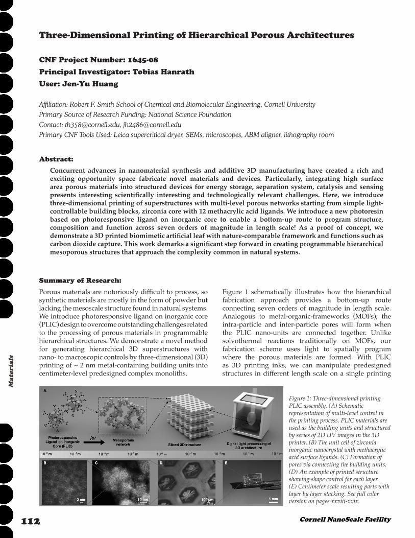
Figure 1: Three-dimensional printing PLIC assembly. (A) Schematic representation of multi-level control in the printing process. PLIC materials are used as the building units and structured by series of 2D UV images in the 3D printer. (B) The unit cell of zirconia inorganic nanocrystal with methacrylic acid surface ligands. (C) Formation of pores via connecting the building units. (D) An example of printed structure showing shape control for each layer. (E) Centimeter scale resulting parts with layer by layer stacking. See full color version on pages xxviii-xxix.
Figure 1 schematically illustrates how the hierarchical fabrication approach provides a bottom-up route connecting seven orders of magnitude in length scale. Analogous to metal-organic-frameworks (MOFs), the intra-particle and inter-particle pores will form when the PLIC nano-units are connected together. Unlike solvothermal reactions traditionally on MOFs, our fabrication scheme uses light to spatially program where the porous materials are formed. With PLIC as 3D printing inks, we can manipulate predesigned structures in different length scale on a single printing
1132017-2018 Research Accomplishments
Materials
procedure. This process combines the inherent porosity of connecting PLIC units at the nanoscale and the advantage of additive manufacturing at macroscopic scale that enables conventional powder-like porous materials be constructed to intricate designed architectures unattainable with conventional fabrication schemes.
The fundamental building block of the PLIC 3D printing resin is based on Zr6O4(OH)4 with 12 methacrylic acid (MAA) ligands (Figure 1A). The structure extends from prominent zirconium-based MOF (UiO-66), possessing attractive thermal and chemical stability with ultrahigh surface area. The methacrylic acid ligands serve two functions: first to provide colloidal stability and second as a molecular connector by photopolymerizing the carbon double bond.
As demonstrated below, we note that additional functionalities can be obtained by exchanging the surface-bound ligands after processing. The inherent compatibility with a broad spectrum of ligand chemistries makes this approach interesting for applications separation applications that rely on programmable interactions between the fluid and the functionalized surface of the particle.
To underscore the practical utility of the mesoporous structures that can be fabricated using the method, we demonstrate the proof-of-concept 3D printing of a highly porous artificial leaf. In nature, the structure of plant leaves has been refined through billion years of evolution to endow all levels of hierarchy from macropores for fluid and nutrient transportation, micropores for gas diffusion and nanopores for gas adsorption to perform complicated and optimal functionalities.
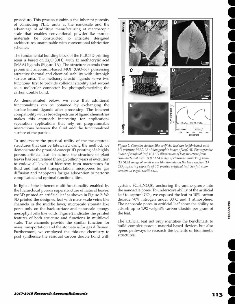
In light of the inherent multi-functionality enabled by the hierarchical porous superstructure of natural leaves, we 3D printed an artificial leaf as shown in Figure 2. We 3D printed the designed leaf with macroscale veins like channels in the middle layer, microscale stomata like pores only on the back surface and nanoscale spongy mesophyll cells like voids. Figure 2 indicates the printed features of both structure and functions in multilevel scale. The channels provide the similar function for mass transportation and the stomata is for gas diffusion. Furthermore, we employed the thio-ene chemistry to post synthesize the residual carbon double bond with
Figure 2: Complex devices like artificial leaf can be fabricated with 3D printing PLIC. (A) Photographic image of leaf. (B) Photographic image of artificial leaf. (C) 3D illustration of leaf structure from cross-sectional view. (D) SEM image of channels mimicking veins. (E) SEM image of small pores like stomata on the back surface (F) CO2 capturing capacity of 3D printed artificial leaf. See full color version on pages xxviii-xxix.
cysteine (C3H7NO2S), anchoring the amine group into the nanoscale pores. To underscore ability of the artificial leaf to capture CO2, we exposed the leaf to 10% carbon dioxide 90% nitrogen under 30°C and 1 atmosphere. The nanoscale pores in artificial leaf show the ability to adsorb up to 1.92 weight% carbon dioxide per gram of the leaf.
The artificial leaf not only identifies the benchmark to build complex porous material-based devices but also opens pathways to research the benefits of biomimetic structures.
114 Cornell NanoScale Facility
Mat
eria
ls
Three-Dimensional Printing of ZnO Macrostructures with Antibacterial Properties and Low Resistivity
CNF Project Number: 1645-08
Principal Investigators: Christopher Kemper Ober1, Tobias Hanrath2
User: Dung-Yi Wu1
Affiliations: 1. Materials Science and Engineering, 2. School of Chemical and Biomolecular Engineering; Cornell UniversityPrimary Source of Research Funding: National Science FoundationContact: [email protected], [email protected]: http://cober.mse.cornell.edu/index.htmlPrimary CNF Tools Used: Scanning electron microscope (SEM)
Abstract:
We report the first 3D-printable ZnO nanoparticles (NPs) for digital light processing that enable the fabrication of arbitrary and complex 3D metal oxide patterns at room temperature. By modifying photosensitive methacrylic acid on ZnO NPs (ZnO-MAA NPs), we demonstrate the continuous production of programmed 3D structures purely from the nanoscale building blocks. The printed image had good resolution and a height variation of only several nanometers. Printed ZnO-MAA NPs possessed better antibacterial properties than commercial PMMA. Also, calcined ZnO structures demonstrate lower resistivity and rectifying behavior.
Summary of Research:
Additive manufacturing, also known as three-dimensional (3D) fabrication, is a rapidly advancing technique that uses layer-by-layer deposition of materials to construct 3D objects [1]. Compared with traditional manufacturing techniques, 3D printing has significant advantages such as the availability of a wide selection of printing materials, the absence of a need for molds and the ability to create highly complex products [2].
In recent years, digital light processing (DLP) has proven to be one of the most promising 3D printing techniques due to its high resolution, faster printing speed and lower manufacturing cost [3]. DLP is analogous to photolithography as they both create structures using a photosensitive material to crosslink the matrix when exposed to ultraviolet (UV) light [4]. Extensive research has focused on printing polymer-based materials for applications such as micro-fluidic devices, biochips and scaffolds [5]. However, printing materials other than organic polymers, such as metal oxides, is still a challenge for the DLP method. Although some research has been devoted to overcoming this material limitations, the main ingredient in this process remains an organic polymer. Therefore, it is essential to develop a way to process inorganic ingredients to broaden the material choice for 3D printing.
Metal oxides possess many impressive properties, such as optical and environmental resistance. ZnO is one of the most commonly studied metal oxide. It is well-known for its wide and direct band gap, transparency, nontoxicity, good stability, antibacterial properties and biocompatibility [6], which enable applications in semiconducting devices, environmental remediation and as antimicrobial agents. Herein, we propose 3D-printable ZnO building blocks having photoresponsive ligands, specifically methacrylic acid (MAA), on the surface of NPs.
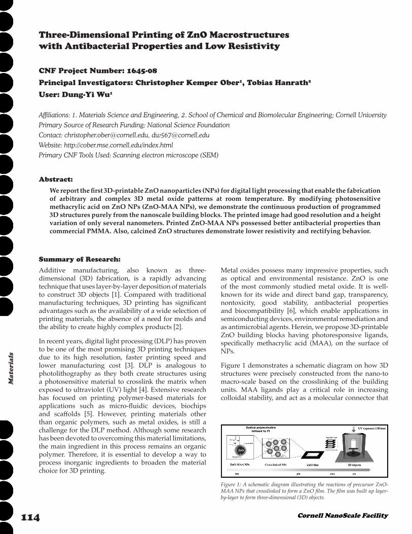
Figure 1 demonstrates a schematic diagram on how 3D structures were precisely constructed from the nano-to macro-scale based on the crosslinking of the building units. MAA ligands play a critical role in increasing colloidal stability, and act as a molecular connector that
Figure 1: A schematic diagram illustrating the reactions of precursor ZnO-MAA NPs that crosslinked to form a ZnO film. The film was built up layer-by-layer to form three-dimensional (3D) objects.
1152017-2018 Research Accomplishments
Materials
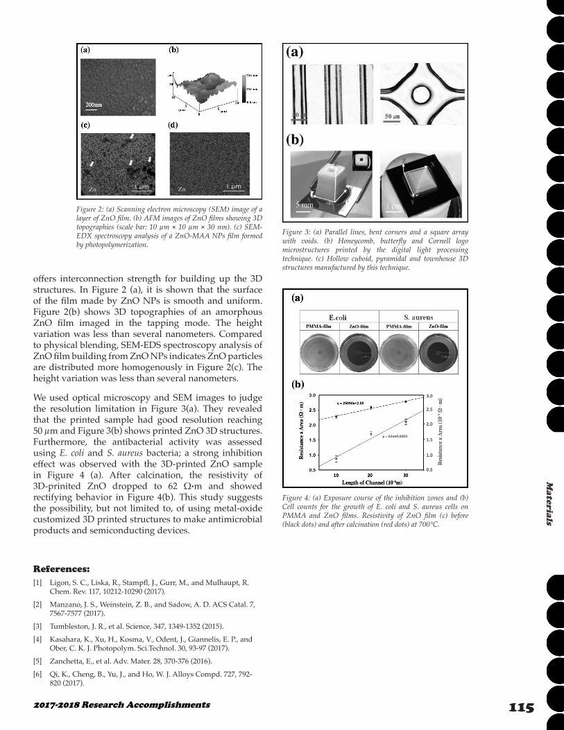
offers interconnection strength for building up the 3D structures. In Figure 2 (a), it is shown that the surface of the film made by ZnO NPs is smooth and uniform. Figure 2(b) shows 3D topographies of an amorphous ZnO film imaged in the tapping mode. The height variation was less than several nanometers. Compared to physical blending, SEM-EDS spectroscopy analysis of ZnO film building from ZnO NPs indicates ZnO particles are distributed more homogenously in Figure 2(c). The height variation was less than several nanometers.
We used optical microscopy and SEM images to judge the resolution limitation in Figure 3(a). They revealed that the printed sample had good resolution reaching 50 µm and Figure 3(b) shows printed ZnO 3D structures. Furthermore, the antibacterial activity was assessed using E. coli and S. aureus bacteria; a strong inhibition effect was observed with the 3D-printed ZnO sample in Figure 4 (a). After calcination, the resistivity of 3D-prinited ZnO dropped to 62 Ω∙m and showed rectifying behavior in Figure 4(b). This study suggests the possibility, but not limited to, of using metal-oxide customized 3D printed structures to make antimicrobial products and semiconducting devices.
References:[1] Ligon, S. C., Liska, R., Stampfl, J., Gurr, M., and Mulhaupt, R.
Chem. Rev. 117, 10212-10290 (2017).
[2] Manzano, J. S., Weinstein, Z. B., and Sadow, A. D. ACS Catal. 7, 7567-7577 (2017).
[3] Tumbleston, J. R., et al. Science, 347, 1349-1352 (2015).
[4] Kasahara, K., Xu, H., Kosma, V., Odent, J., Giannelis, E. P., and Ober, C. K. J. Photopolym. Sci.Technol. 30, 93-97 (2017).
[5] Zanchetta, E., et al. Adv. Mater. 28, 370-376 (2016).
[6] Qi, K., Cheng, B., Yu, J., and Ho, W. J. Alloys Compd. 727, 792-820 (2017).
Figure 4: (a) Exposure course of the inhibition zones and (b) Cell counts for the growth of E. coli and S. aureus cells on PMMA and ZnO films. Resistivity of ZnO film (c) before (black dots) and after calcination (red dots) at 700°C.
Figure 2: (a) Scanning electron microscopy (SEM) image of a layer of ZnO film. (b) AFM images of ZnO films showing 3D topographies (scale bar: 10 µm × 10 µm × 30 nm). (c) SEM-EDX spectroscopy analysis of a ZnO-MAA NPs film formed by photopolymerization.
Figure 3: (a) Parallel lines, bent corners and a square array with voids. (b) Honeycomb, butterfly and Cornell logo microstructures printed by the digital light processing technique. (c) Hollow cuboid, pyramidal and townhouse 3D structures manufactured by this technique.
116 Cornell NanoScale Facility
Mat
eria
ls
Novel Platform for Characterization of Nanostructured Polymer Brushes
CNF Project Number: 1757-09
Principal Investigator: Christopher Kemper Ober2
User: Wei-Liang Chen1,2
Affiliations: 1. School of Chemical and Biomolecular Engineering, 2. Department of Materials Science and Engineering; Cornell University
Primary Source of Research Funding: National Science FoundationContact: [email protected], [email protected]: http://cober.mse.cornell.edu/index.htmlPrimary CNF Tools Used: ASML 300C DUV stepper, SC4500 evaporator, Oxford PlasmaLab 80+ etch system,
ZEISS SEM, Oxford ALD FlexAL, Unaxis 770 deep silicon etcher, Veeco Icon AFM
Abstract:
For further characterization of polymer brushes by neutron and laser scattering, a specific platform was fabricated. The platform allows the anchoring of the polymer brushes on the sidewall of the trenches only, which makes the scattering signals responsive to the change of the polymer brush morphologies. Such methods could increase the sensitivity of the characterization and make probing of more complicated structures possible. Poly(2-(dimethylamino)ethyl methacrylate) brushes were synthesized by atom transfer radical polymerization on the grating. The polymer brushes grown on the sidewall have gradient profiles with a maximum thickness at the bottom of the grating, which is due to the lack of confinement on the top. Such a platform lays down the foundation for the future characterization.
Summary of Research:
Polymer brushes have already demonstrated their application in many fields and their structures have been studied widely in different conditions as described [1]. However, studies focusing on the more complicated structures of polymer brushes, such as molecular brushes, are still in need. It is critical to characterize the polymer brushes in wet state since the tension applied on them is amplified and thus forms more ordered structures. This requirement inspires us to develop a platform, which has polymer brushes anchored on the sidewall of the grating only. When having such platforms in the wet medium, the morphological change of the polymer brushes then controls the opening of the grating which could subsequently be captured by laser and neutron scattering [2]. By using the grating, the response of the polymer brushes would be amplified and allow us to reveal more details in polymer brush structures.
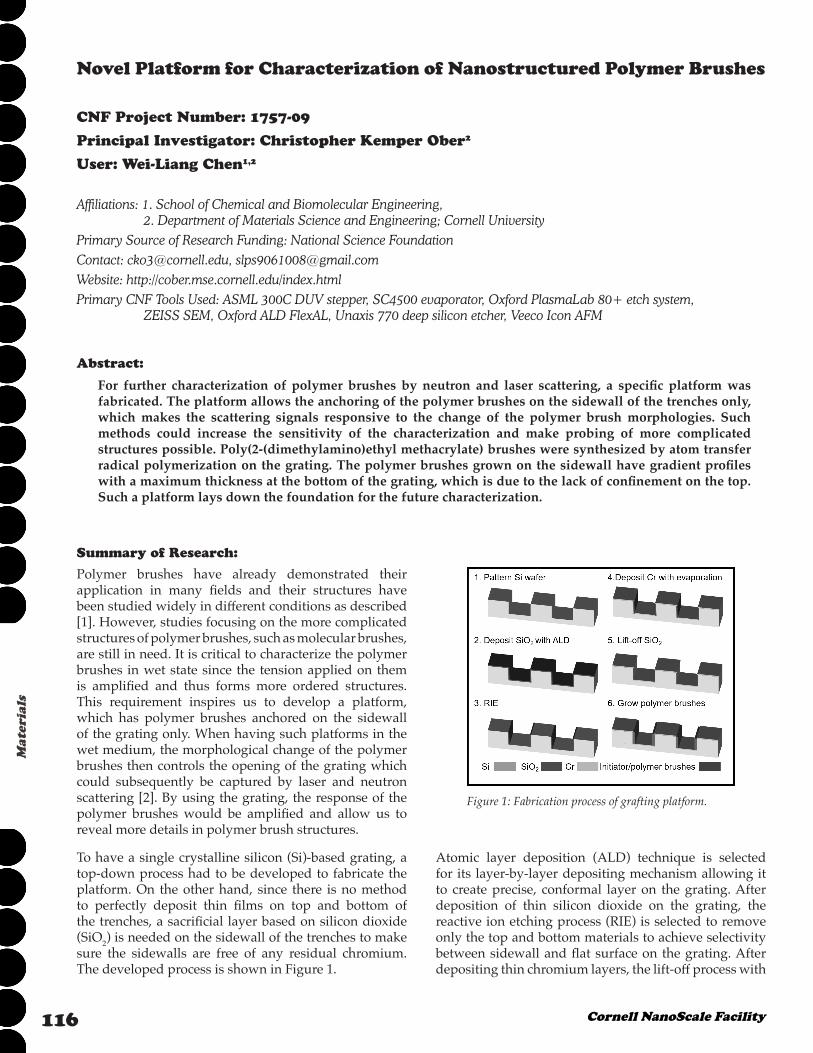
To have a single crystalline silicon (Si)-based grating, a top-down process had to be developed to fabricate the platform. On the other hand, since there is no method to perfectly deposit thin films on top and bottom of the trenches, a sacrificial layer based on silicon dioxide (SiO2) is needed on the sidewall of the trenches to make sure the sidewalls are free of any residual chromium. The developed process is shown in Figure 1.
Figure 1: Fabrication process of grafting platform.
Atomic layer deposition (ALD) technique is selected for its layer-by-layer depositing mechanism allowing it to create precise, conformal layer on the grating. After deposition of thin silicon dioxide on the grating, the reactive ion etching process (RIE) is selected to remove only the top and bottom materials to achieve selectivity between sidewall and flat surface on the grating. After depositing thin chromium layers, the lift-off process with
1172017-2018 Research Accomplishments
Materials
hydrofluoric acid could remove undesired chromium on the sidewall and the required grating is obtained for the growth of sidewall-only polymer brushes.
The ALD formed SiO2 is tuned to have a low density that facilitates the lift-off. The target chromium film thickness is still 5 nm for preservation of the grating original dimension.
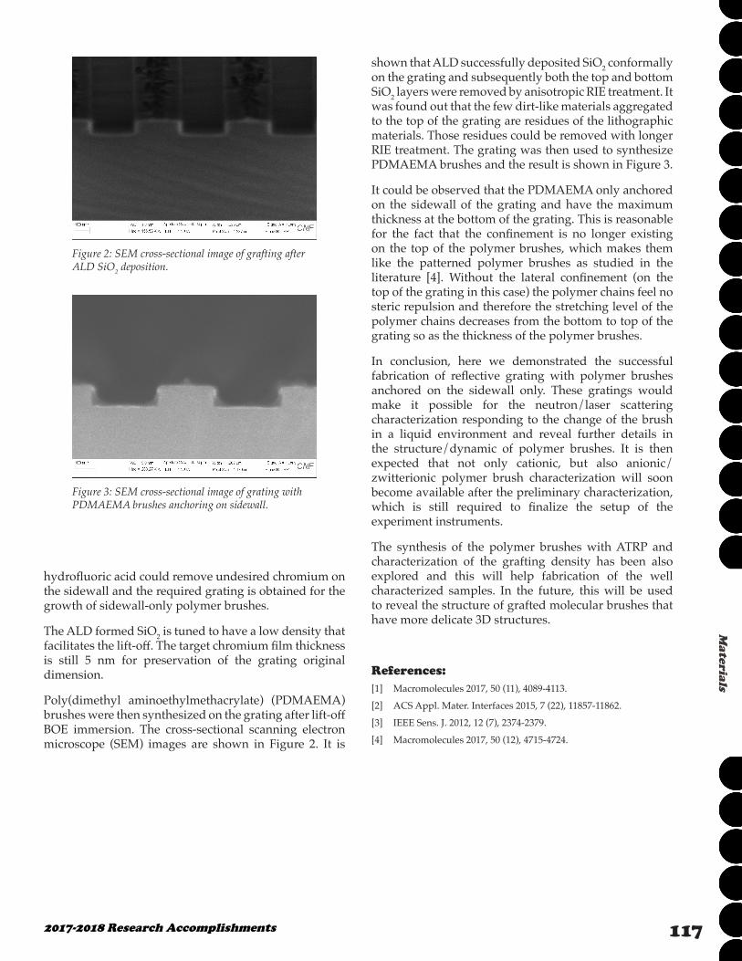
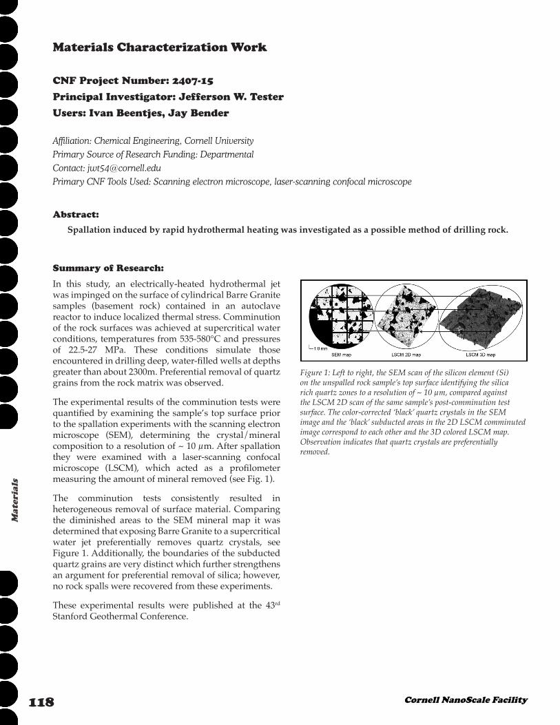
Poly(dimethyl aminoethylmethacrylate) (PDMAEMA) brushes were then synthesized on the grating after lift-off BOE immersion. The cross-sectional scanning electron microscope (SEM) images are shown in Figure 2. It is
shown that ALD successfully deposited SiO2 conformally on the grating and subsequently both the top and bottom SiO2 layers were removed by anisotropic RIE treatment. It was found out that the few dirt-like materials aggregated to the top of the grating are residues of the lithographic materials. Those residues could be removed with longer RIE treatment. The grating was then used to synthesize PDMAEMA brushes and the result is shown in Figure 3.
It could be observed that the PDMAEMA only anchored on the sidewall of the grating and have the maximum thickness at the bottom of the grating. This is reasonable for the fact that the confinement is no longer existing on the top of the polymer brushes, which makes them like the patterned polymer brushes as studied in the literature [4]. Without the lateral confinement (on the top of the grating in this case) the polymer chains feel no steric repulsion and therefore the stretching level of the polymer chains decreases from the bottom to top of the grating so as the thickness of the polymer brushes.
In conclusion, here we demonstrated the successful fabrication of reflective grating with polymer brushes anchored on the sidewall only. These gratings would make it possible for the neutron/laser scattering characterization responding to the change of the brush in a liquid environment and reveal further details in the structure/dynamic of polymer brushes. It is then expected that not only cationic, but also anionic/zwitterionic polymer brush characterization will soon become available after the preliminary characterization, which is still required to finalize the setup of the experiment instruments.
The synthesis of the polymer brushes with ATRP and characterization of the grafting density has been also explored and this will help fabrication of the well characterized samples. In the future, this will be used to reveal the structure of grafted molecular brushes that have more delicate 3D structures.
References:[1] Macromolecules 2017, 50 (11), 4089-4113.
[2] ACS Appl. Mater. Interfaces 2015, 7 (22), 11857-11862.
[3] IEEE Sens. J. 2012, 12 (7), 2374-2379.
[4] Macromolecules 2017, 50 (12), 4715-4724.
Figure 3: SEM cross-sectional image of grating with PDMAEMA brushes anchoring on sidewall.
Figure 2: SEM cross-sectional image of grafting after ALD SiO2 deposition.
118 Cornell NanoScale Facility
Mat
eria
ls
Materials Characterization Work
CNF Project Number: 2407-15
Principal Investigator: Jefferson W. Tester
Users: Ivan Beentjes, Jay Bender
Affiliation: Chemical Engineering, Cornell UniversityPrimary Source of Research Funding: DepartmentalContact: [email protected] CNF Tools Used: Scanning electron microscope, laser-scanning confocal microscope
Abstract:
Spallation induced by rapid hydrothermal heating was investigated as a possible method of drilling rock.
Summary of Research:
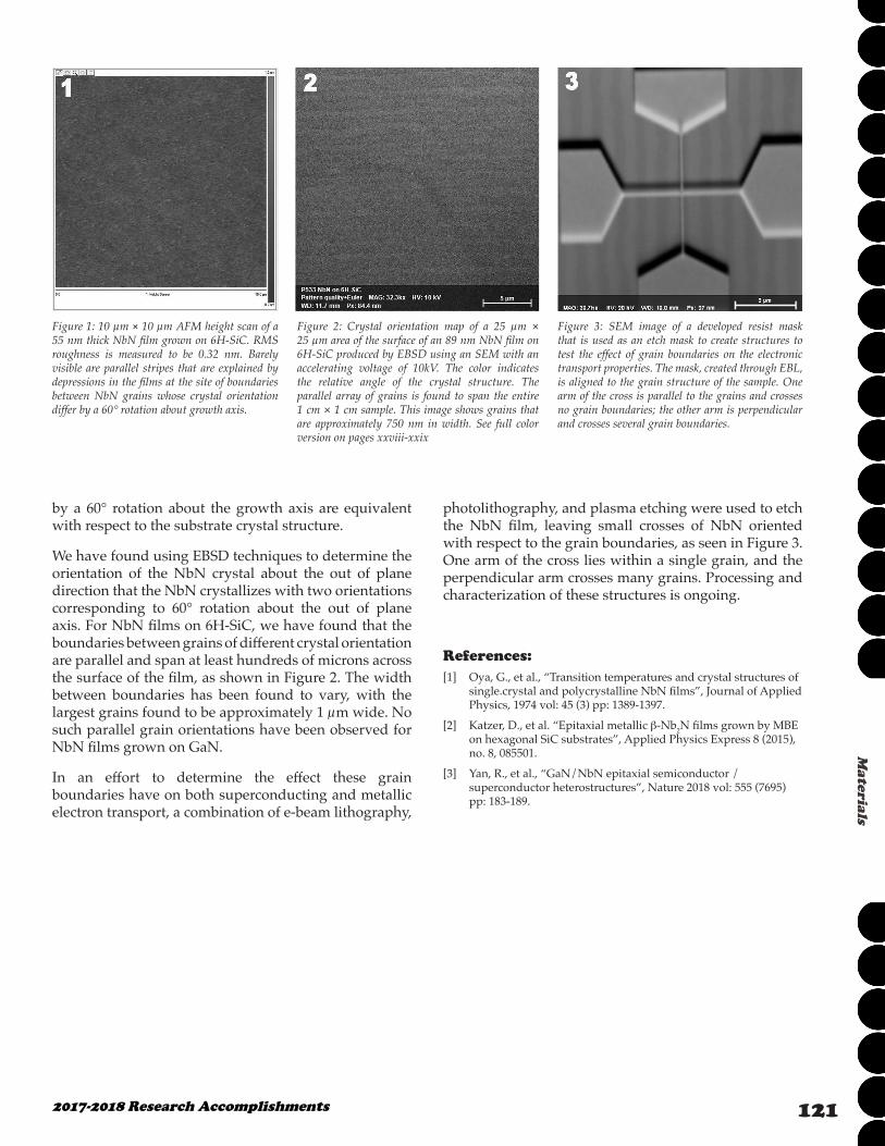
Figure 1: Left to right, the SEM scan of the silicon element (Si) on the unspalled rock sample’s top surface identifying the silica rich quartz zones to a resolution of ~ 10 µm, compared against the LSCM 2D scan of the same sample’s post-comminution test surface. The color-corrected ‘black’ quartz crystals in the SEM image and the ‘black’ subducted areas in the 2D LSCM comminuted image correspond to each other and the 3D colored LSCM map. Observation indicates that quartz crystals are preferentially removed.
In this study, an electrically-heated hydrothermal jet was impinged on the surface of cylindrical Barre Granite samples (basement rock) contained in an autoclave reactor to induce localized thermal stress. Comminution of the rock surfaces was achieved at supercritical water conditions, temperatures from 535-580°C and pressures of 22.5-27 MPa. These conditions simulate those encountered in drilling deep, water-filled wells at depths greater than about 2300m. Preferential removal of quartz grains from the rock matrix was observed.
The experimental results of the comminution tests were quantified by examining the sample’s top surface prior to the spallation experiments with the scanning electron microscope (SEM), determining the crystal/mineral composition to a resolution of ~ 10 µm. After spallation they were examined with a laser-scanning confocal microscope (LSCM), which acted as a profilometer measuring the amount of mineral removed (see Fig. 1).
The comminution tests consistently resulted in heterogeneous removal of surface material. Comparing the diminished areas to the SEM mineral map it was determined that exposing Barre Granite to a supercritical water jet preferentially removes quartz crystals, see Figure 1. Additionally, the boundaries of the subducted quartz grains are very distinct which further strengthens an argument for preferential removal of silica; however, no rock spalls were recovered from these experiments.
These experimental results were published at the 43rd Stanford Geothermal Conference.

1192017-2018 Research Accomplishments
Materials

120 Cornell NanoScale Facility
Mat
eria
ls
Growth and Characterization of NbN/III-N Heterostructures by Molecular Beam Epitaxy
CNF Project Number: 2443-16
Principal Investigators: Debdeep Jena, Huili Grace Xing
User: John Wright
Affiliation(s): Materials Science and Engineering, Electrical and Computer Engineering; Cornell UniversityPrimary Sources of Research Funding: ONR grant #N00014-17-1-2414 monitored by Dr. Paul Maki
is gratefully acknowledged; CCMR Seed DMR-1120296Contact: [email protected], [email protected], [email protected] CNF Tools Used: Veeco Icon AFM, Zeiss SEM, e-beam evaporators, AJA sputter deposition,
Oxford 81 etcher, PT770 etcher, JEOL 9500, ABM contact aligner, Autostep i-line stepper
Abstract:
Films of the metallic superconductor niobium nitride (NbN) have been grown on 6H-SiC substrate and GaN substrate. The surface morphology, grain structure, and electronic transport properties of the films are characterized and used to optimize the growth conditions with the goal of fabricating epitaxial heterostructures incorporating NbN and the III-N family of semiconductors.
Summary of Research:
NbN is a metallic type-II superconductor that can crystallize in both cubic and hexagonal crystal structures [1]. It has been demonstrated [2] that NbN can be grown epitaxially on silicon carbide (SiC) and gallium nitride (GaN) substrates by molecular beam epitaxy (MBE). Multilayer structures incorporating NbN, GaN, and AlN have also been produced and used to demonstrate the possibility of semiconductor devices integrating epitaxial superconducting thin films [3].
In this work we have characterized NbN thin films and NbN/GaN heterostructures grown by MBE using atomic force microscopy (AFM), x-ray diffraction (XRD), electronic transport measurements, and electron backscatter diffraction (EBSD) techniques. We demonstrate that by altering growth conditions such as Nb/N ratio, growth rate, and substrate temperature, the surface morphology, lattice parameters, stoichiometry, and superconducting properties of NbN thin films can be controlled. The goal of this project is to enable the controlled growth of NbN/III-N heterostructures. To enable the growth of III-N semiconductor films with sufficiently low defect density that electronic properties are not significantly degraded the growth of NbN films must be optimized to achieve smooth, continuous, and highly crystalline and epitaxial films.
Our MBE system utilizes an electron beam evaporator to provide Nb flux, while standard effusion cells can used to provide Ga, Al, In, and various dopant materials. The nitrogen is provided by an RF plasma source.
The CNF Veeco Icon AFM has been used to study the surface morphology. With the goal of producing epitaxial heterojunctions with atomically sharp interfaces the surface morphology of the NbN thin films as measured by AFM is considered an important material parameter to optimize. By controlling deposition temperature, growth rate, and Nb/N ratio we have produced NbN films on 6H-SiC and measured RMS roughness below 0.5 nm by AFM over a scan area of 10 µm × 10 µm, as shown in Figure 1.
NbN crystallizes in many polymorphs. Asymmetric XRD diffraction analysis indicates that the NbN films primarily possess cubic crystal symmetry oriented with the <111> crystallographic axis aligned to the growth axis. GaN possesses the wurtzite hexagonal structure, and 6H-SiC possesses a similar hexagonal structure, with the <0001> crystallographic axis aligned to the growth direction in both cases. This means that for both growth on GaN and 6H-SiC, the NbN films have lower order symmetry about the growth axis then does the substrate. Therefore, two orientations of the NbN crystal differing
1212017-2018 Research Accomplishments
Materials
by a 60° rotation about the growth axis are equivalent with respect to the substrate crystal structure.
We have found using EBSD techniques to determine the orientation of the NbN crystal about the out of plane direction that the NbN crystallizes with two orientations corresponding to 60° rotation about the out of plane axis. For NbN films on 6H-SiC, we have found that the boundaries between grains of different crystal orientation are parallel and span at least hundreds of microns across the surface of the film, as shown in Figure 2. The width between boundaries has been found to vary, with the largest grains found to be approximately 1 µm wide. No such parallel grain orientations have been observed for NbN films grown on GaN.
In an effort to determine the effect these grain boundaries have on both superconducting and metallic electron transport, a combination of e-beam lithography,
photolithography, and plasma etching were used to etch the NbN film, leaving small crosses of NbN oriented with respect to the grain boundaries, as seen in Figure 3. One arm of the cross lies within a single grain, and the perpendicular arm crosses many grains. Processing and characterization of these structures is ongoing.
References:[1] Oya, G., et al., “Transition temperatures and crystal structures of
single.crystal and polycrystalline NbN films”, Journal of Applied Physics, 1974 vol: 45 (3) pp: 1389-1397.
[2] Katzer, D., et al. “Epitaxial metallic β-Nb2N films grown by MBE on hexagonal SiC substrates”, Applied Physics Express 8 (2015), no. 8, 085501.
[3] Yan, R., et al., “GaN/NbN epitaxial semiconductor / superconductor heterostructures”, Nature 2018 vol: 555 (7695) pp: 183-189.
Figure 3: SEM image of a developed resist mask that is used as an etch mask to create structures to test the effect of grain boundaries on the electronic transport properties. The mask, created through EBL, is aligned to the grain structure of the sample. One arm of the cross is parallel to the grains and crosses no grain boundaries; the other arm is perpendicular and crosses several grain boundaries.
Figure 1: 10 µm × 10 µm AFM height scan of a 55 nm thick NbN film grown on 6H-SiC. RMS roughness is measured to be 0.32 nm. Barely visible are parallel stripes that are explained by depressions in the films at the site of boundaries between NbN grains whose crystal orientation differ by a 60° rotation about growth axis.
Figure 2: Crystal orientation map of a 25 µm × 25 µm area of the surface of an 89 nm NbN film on 6H-SiC produced by EBSD using an SEM with an accelerating voltage of 10kV. The color indicates the relative angle of the crystal structure. The parallel array of grains is found to span the entire 1 cm × 1 cm sample. This image shows grains that are approximately 750 nm in width. See full color version on pages xxviii-xxix

122 Cornell NanoScale Facility
Mat
eria
ls
Nanotube Transistor Arrays on a TEM Substrate
CNF Project Numbers: 2486-16, 900-00
Principal Investigators: Jonathan Alden, Paul L. McEuen
Users: Jonathan S. Alden, Joshua S. Alden, Alejandro J. Cortese
Affiliations: Esper Biosciences, Inc; Department of Physics, Cornell UniversityPrimary Source of Research Funding: National Institutes of Health, National Science FoundationContact: [email protected], [email protected], [email protected], [email protected] CNF Tools Used: Low pressure chemical vapor deposition (LPCVD) furnaces (oxide, nitride),
Autostep i-line stepper, ABM contact aligner, SC4500 evaporators, Oxford 80 RIE
Abstract:
We use photolithography to fabricate nanotube transistor devices on substrates with thin nitride windows, which can be imaged using transmission electron microscopy (TEM). Our device architecture permits us to characterize a given nanotube both electrically, and by high-resolution TEM. In low-dimensional systems, such as nanotubes, where nanoscale surface and defect structure can have profound influences on the electrical properties, we expect this combined nanoscale imaging and electrical characterization to yield insights that will inform the design of nanoscale sensors.
Summary of Research:
Figure 1: Optical image of microfabricated TEM grid with 26 pairs of source-drain electrodes, a top gate, and a thin nitride window for TEM imaging after top-gate is removed via chemical etching.
The study of low-dimensional materials, such as carbon nanotubes, graphene, and molybdenum disulfide, has been an area of growing interest over the past decades, in part due to their promise as molecular sensors. Due to their one-to-few-atom thickness, the properties of such materials often depend sensitively on surface adsorbates, substrate-surface interaction and defect structure. Improving sample cleanliness, for example, enabled the first observations of spin-orbit coupling in carbon nanotubes [1] and, more recently, the fractal quantum Hall effect, known as Hofstadter’s butterfly, in graphene [2]. In order to understand these nanoscale structures and subsequently design improved sensors, a device architecture is needed that combines the atomic-level characterization afforded by TEM with the electronics characterization ability enabled by a gated, transistor-like geometry.
We demonstrate that we can produce arrays of gated nanotube sensors devices, with reasonably high yield that can be characterized afterwards by TEM. Our design also keeps parasitic capacitance from our electrodes to the highly resistive silicon substrate low enough to enable electronic measurements of our transistors at MHz bandwidth.
We fabricate nanotube devices on TEM grids using a combination of photolithography and standard nanotube growth and transfer techniques [3]. Figure 1 shows one of such devices, having 26 source-drain electrode pairs and two top gates. Between a few of
the electrode pairs are individual nanotubes, which have been transferred prior to the deposition of a gate dielectric, and top-gate. The device fabrication involves using nine masks to define the various structures, which have been designed to yield nanotube devices with good gating characteristics, as well as low capacitive coupling between nearby electrodes.

1232017-2018 Research Accomplishments
Materials
The outline of the fabrication procedure is as follows. We begin by using low pressure chemical vapor deposition (LP CVD) to deposit the low-stress nitride on a 300 µm-thick silicon substrate, which will ultimately become our TEM window. We later deposit electrodes, and use backside alignment followed by reactive ion etching (RIE) to expose rectangles on the back of the wafer that will later be used for a potassium hydroxide (KOH) through-etch. Arrays of parallel nanotubes are grown by CVD on a separate quartz substrate, coated with poly(methyl methacrylate) (PMMA), lifted off with KOH, and transferred onto the device substrate [3], where unwanted areas are patterned and etched using RIE. We use atomic layer deposition (ALD) to deposit a gate dielectric, after which we pattern and evaporate a gold top-gate. The surface is then coated with a KOH protection layer, and the devices are placed in hot KOH, which etches the silicon exposed on the back, to both release individual grids and to etch the silicon away from behind the nitride window. Later, the nanotube devices will be imaged through this window using TEM. The protection layer is then removed, and the grids are cleaned with oxygen plasma. Our fabrication process typically yields at least one electrically-connected, gated nanotube on 75% of the TEM grids.
Furthermore, we can probe the electrical characteristics at high speeds in the MHz range. Previous research has shown that single charge fluctuations in a dielectric can be detected by semiconducting carbon nanotubes as random telegraph signals [4]. As show in Figure 3, our devices are also capable of measuring such signals, but at higher speeds with rise times less than 1 µs.
After characterizing the nanotubes electronically, we can etch away the gold top-gate, and image them by TEM to determine, for example, the nanotube diameter. Figure 4 shows one such nanotube, which can be seen to be single-walled (single dark lines running parallel to the arrows), and 4 nm in diameter (the width between those lines).
In principle, our fabrication procedure can be applied to many different CVD-grown low-dimensional materials with only minor modifications, and may lead to the development of improved nanoscale sensors capable of high-speed molecular sensing.
References:[1] F. Kuemmeth, et al., Nature 452 448-452 (2008).
[2] C. R. Dean, et al., Nature 497, 598-602 (2013).
[3] L. Jiao, et al., J. Am. Chem. Soc. 130, 12612-12613 (2008).
[4] T. Sharf, et al., Nano Lett. 14 (9) 4925-4930 (2014).
Figure 4: TEM image of a nanotube imaged through a thin nitride window, after top-gate removal.
Figure 2: Upper: SEM image of nanotubes between source-drain electrodes, passing over thin nitride windows. Lower: Corresponding conductance measurements as a function of top gate voltage showing six conducting nanotubes with varying characteristics.
Figure 2 shows an SEM image of nanotubes patterned between the source-drain electrode pairs, imaged prior to top-gate deposition. The squares in the center are thin nitride windows for low-background TEM imaging. After completion of the device fabrication, these nanotubes are characterized electrically, shown in the lower portion of Figure 2. All of these nanotubes can be gated to have resistance lower than 1 MΩ (50kΩ/µm) showing that they have a low defect density, and good coupling to the top gate. Nanotubes 1 and 2 can be seen to be metallic, while nanotubes 3-6 are semiconducting.
Figure 3: High-speed measurement of nanotube random telegraph signal showing (a) fluctuations in nanotube current and (b) measured rise time of less than 1 µs.
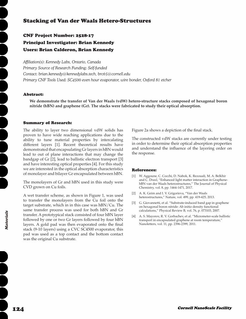
124 Cornell NanoScale Facility
Mat
eria
ls
Stacking of Van der Waals Hetero-Structures
CNF Project Number: 2528-17
Principal Investigator: Brian Kennedy
Users: Brian Calderon, Brian Kennedy
Affiliation(s): Kennedy Labs, Ontario, CanadaPrimary Source of Research Funding: Self-fundedContact: [email protected], [email protected] CNF Tools Used: SC4500 even hour evaporator, wire bonder, Oxford 81 etcher
Abstract:
We demonstrate the transfer of Van der Waals (vdW) hetero-structure stacks composed of hexagonal boron nitride (hBN) and graphene (Gr). The stacks were fabricated to study their optical absorption.
Summary of Research:
The ability to layer two dimensional vdW solids has proven to have wide reaching applications due to the ability to tune material properties by intercalating different layers [1]. Recent theoretical results have demonstrated that encapsulating Gr layers in hBN would lead to out of plane interactions that may change the bandgap of Gr [2], lead to ballistic electron transport [3] and have interesting optical properties [4]. For this study we are interested in the optical absorption characteristics of monolayer and bilayer Gr encapsulated between hBN.
The monolayers of Gr and hBN used in this study were CVD grown on Cu foils.
A wet transfer scheme, as shown in Figure 1, was used to transfer the monolayers from the Cu foil onto the target substrate, which in in this case was hBN/Cu. The same transfer process was used for both hBN and Gr transfer. A prototypical stack consisted of four hBN layer followed by one or two Gr layers followed by four hBN layers. A gold pad was then evaporated onto the final stack (9-10 layers) using a CVC SC4500 evaporator, this pad was used as a top contact and the bottom contact was the original Cu substrate.
Figure 2a shows a depiction of the final stack.
The constructed vdW stacks are currently under testing in order to determine their optical absorption properties and understand the influence of the layering order on the response.
References:[1] W. Aggoune, C. Cocchi, D. Nabok, K. Rezouali, M. A. Belkhir
and C. Draxl, “Enhanced light matter interaction in Graphene-hBN van der Waals heterostructures,” The Journal of Physical Chemistry, vol. 8, pp. 1464-1471, 2017.
[2] A. K. Geim and I. V. Grigorieva, “Van der Waals heterostructures,” Nature, vol. 499, pp. 419-425, 2013.
[3] G. Giovannetti, et al. “Substrate-induced band gap in graphene on hexagonal boron nitride: Ab initio density functional calculations,” Physical Review B, vol. 76, p. 073103, 2007.
[4] A. S. Mayorov, R. V. Gorbachev, et al. “Micrometer-scale ballistic transport in encapsulated graphene at room temperature,” Nanoletters, vol. 11, pp. 2396-2399, 2011.
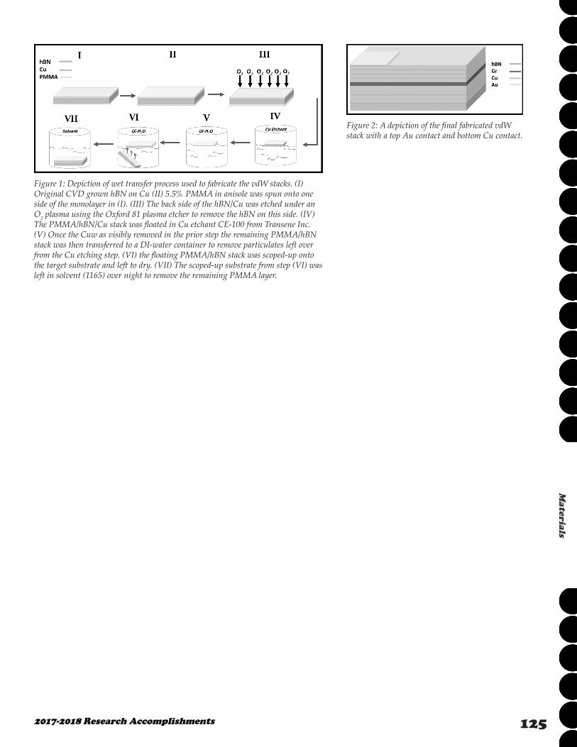
1252017-2018 Research Accomplishments
Materials
Figure 2: A depiction of the final fabricated vdW stack with a top Au contact and bottom Cu contact.
Figure 1: Depiction of wet transfer process used to fabricate the vdW stacks. (I) Original CVD grown hBN on Cu (II) 5.5% PMMA in anisole was spun onto one side of the monolayer in (I). (III) The back side of the hBN/Cu was etched under an O2 plasma using the Oxford 81 plasma etcher to remove the hBN on this side. (IV) The PMMA/hBN/Cu stack was floated in Cu etchant CE-100 from Transene Inc. (V) Once the Cuw as visibly removed in the prior step the remaining PMMA/hBN stack was then transferred to a DI-water container to remove particulates left over from the Cu etching step. (VI) the floating PMMA/hBN stack was scoped-up onto the target substrate and left to dry. (VII) The scoped-up substrate from step (VI) was left in solvent (1165) over night to remove the remaining PMMA layer.

126 Cornell NanoScale Facility
Mat
eria
ls
Characterization of Hexagonal Boron Nitride Thin Films Grown by Molecular Beam Epitaxy
CNF Project Number: 2562-17
Principal Investigator: Dr. Debdeep Jena
User: Ryan Page
Affiliation(s): Department of Materials Science and Engineering, School of Electrical and Computer Engineering; Cornell University
Primary Source of Research Funding: Air Force Office of Scientific ResearchContact: [email protected], [email protected] CNF Tools Used: Veeco Icon AFM, SC4500 odd-hour evaporator
Abstract:
Hexagonal boron nitride (hBN) is a layered material with a wide variety of promising applications, from being used as a substrate and dielectric in Van der Waals heterostructures, to hosting bright, room temperature single photon emitters. Here we report molecular beam epitaxy (MBE) growth and characterization of hBN thin films on sapphire substrates. Films up to 20 nm thick were grown at substrate temperatures up to 1750°C to study the interplay between substrate temperature and source material flux on the morphology and crystallinity of the films. It was observed that films grown at high temperatures (greater than 1650°C) and low boron fluxes (3E-9 torr beam equivalent pressure) resulted in the smoothest and highest quality films. Films were characterized extensively in the Cornell NanoScale Science and Technology Facility using the Veeco Icon atomic force microscope.
Summary of Research:
Figure 1: Atomic force microscope image of lower substrate temperature (1600°C) hBN film shows rough, polycrystalline morphology. Inset: diffuse, ringed RHEED pattern.
Hexagonal boron nitride (hBN) is an atomically thin crystalline material, isostructural to graphene, consisting of sheets of boron and nitrogen atoms arranged into a two-dimensional hexagonal net. While the in-plane bonds between each boron and nitrogen atoms in each sheet are very strong, the sheets themselves are bound to one another only by weak Van der Waals forces. Hexagonal boron nitride, along with other so-called two-dimensional materials such as graphene and the family of transition metal dichalcogenides (TMDs) have been the subject of intense research interest in recent years due to the prospect of devices and heterostructures based on stacked monolayers of different 2D materials [1]. The realization of such devices and applications will depend critically on hBN for use as a substrate and dielectric layer. Additionally, hBN has applications in deep ultraviolet photonics and lighting, exhibiting strong emission in the UV-C spectrum [2]. Finally, point defects in hBN layers have recently been discovered as bright, room temperature single photon emitters, opening up this material to applications in quantum cryptography and precision sensing [3].
Despite all of these applications, the synthesis of hBN, particularly epitaxial layers, has proven to be a challenge. In this work, we focus on the growth and characterization of hBN thin films grown by molecular beam epitaxy (MBE) on sapphire substrates. The films are grown at ultra-high substrate temperatures (1600 to 1800°C) in order to overcome kinetic barriers of the crystal growth. The quality and morphology of the films were studied extensively with the Veeco Icon
1272017-2018 Research Accomplishments
Materials
Figure 4: Raman spectrum of hBN film grown on sapphire exhibits clear hBN E2g peak near 1365 1/cm. Spectrum of sapphire substrate shown for comparison.
Figure 2: Atomic force microscope image of higher substrate temperature (1650°C) hBN shows smooth surface with network of ripple-like folds, line height profile of inset line shown above. Inset: bright, streaked RHEED pattern.
Figure 3: X-ray photoelectron spectroscopy of hexagonal boron nitride grown on sapphire confirms the chemical composition of the film is 1:1 boron to nitrogen.
atomic force microscope (AFM). The films were also characterized by Raman spectroscopy, ultraviolet absorption spectroscopy, spectroscopic ellipsometry, and x-ray photoelectron spectroscopy to elucidate their structural, optical, and chemical properties. To study the effect of MBE growth conditions (e.g. boron and nitrogen fluxes and substrate temperature) on the morphology and quality of the films, films throughout the growth parameter space were grown. We observed a variety of different surface morphologies, wherein several trends are noted: at lower temperatures (less than 1600°C) the hBN films consistently exhibited visible rings in the in situ reflection high energy electron diffraction (RHEED) patterns, indicating a polycrystalline growth mode. Subsequently, these films had very rough surface morphologies as seen in the AFM. At higher temperatures (1600 to 1750°C), clear streaks were seen in the RHEED pattern, suggesting a higher quality film growth, while we observed in the AFM images smooth films with a dense network of ripple-like features. These ripples have been reported in hBN flakes grown by chemical vapor deposition, where they are attributed to the thermal expansion mismatch between the hBN and the substrate causing the hBN to wrinkle and fold up on itself [4]. At each temperature range, there was an incident boron flux, provided by a high temperature boron effusion cell, past which the films would also become rough and polycrystalline. At all temperatures, this threshold flux was very low (approx. 3E-9 torr beam equivalent pressure), but it increased with temperature. All growths are done in excess nitrogen conditions using a radio frequency plasma nitrogen source.
X-ray photoelectron spectroscopy of these films confirmed a 1:1 boron to nitrogen ratio with no evidence of carbon contamination. The films also exhibit a sharp absorption peak centered near 6 eV, the band gap of hBN. In the Raman spectra, the hBN E2g peak is observed near 1365 1/cm, confirming the phase of the grown films. Notably, hBN was also grown with isotopically purified nitrogen-15; the E2g peak exhibited an approximately 15 1/cm redshift corresponding to the heavier atoms. The demonstrated isotopic control in the films allows for future studies into the electron-phonon interactions of hBN.
In conclusion, hexagonal boron nitride thin films were grown by molecular beam epitaxy and characterized by a variety of techniques to probe the structural, chemical, and optical properties of the layers. It was found that ultra-high growth temperatures and low boron fluxes produce the highest quality films. This work represents a step toward the integration of high quality hBN into a wide range of devices and applications.
References:[1] Geim, A., and Grigorieva, I. Nature 499, 419-425 (2013).
[2] Watanabe, K., Taniguchi, T., and Kanda, H. Nature Materials 3, 404-409 (2004).
[3] Jungwirth, N., Calderon, B., Ji, Y., et al. Nano Lett. 16, 6052-6057 (2016).
[4] Kim, K., Hsu, A. Jia, X., et al. Nano Lett. 12, 161.166 (2012).
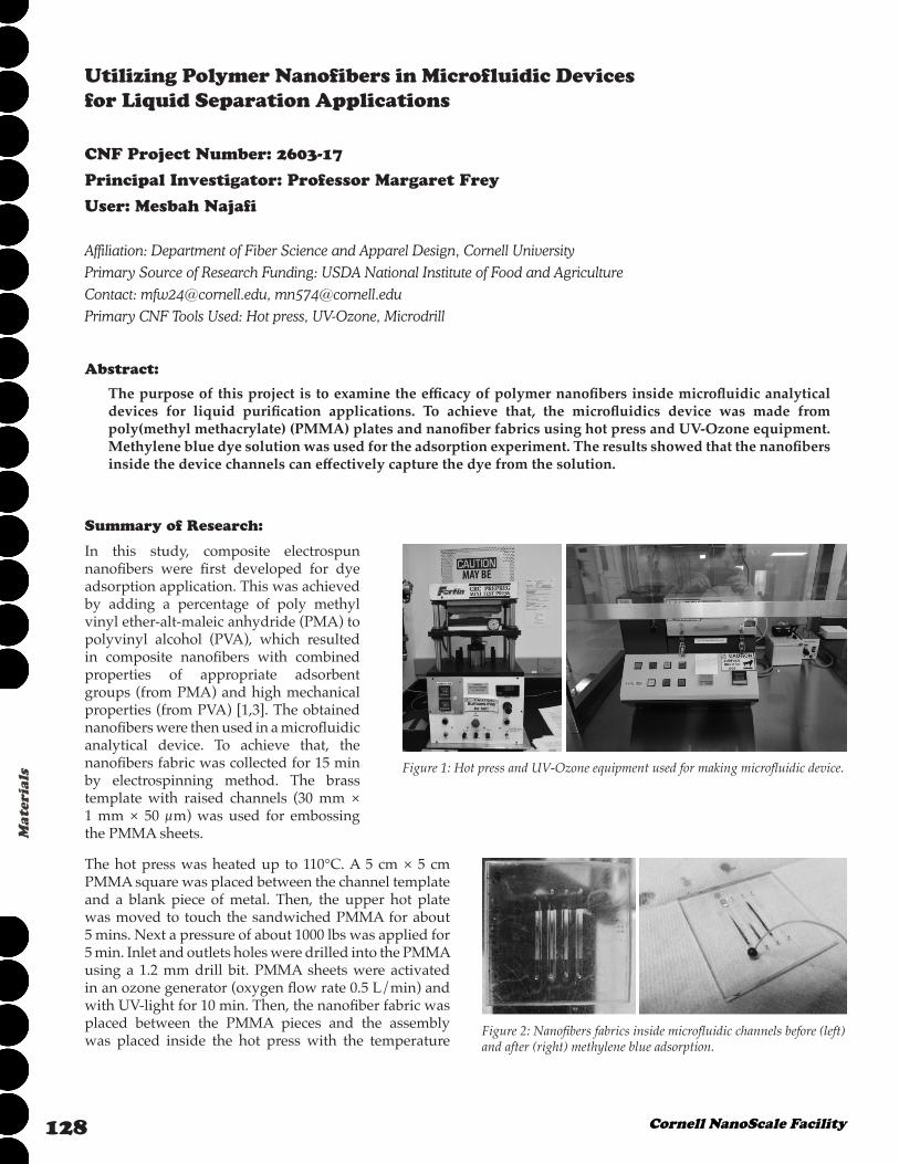
128 Cornell NanoScale Facility
Mat
eria
ls
Utilizing Polymer Nanofibers in Microfluidic Devices for Liquid Separation Applications
CNF Project Number: 2603-17
Principal Investigator: Professor Margaret Frey
User: Mesbah Najafi
Affiliation: Department of Fiber Science and Apparel Design, Cornell UniversityPrimary Source of Research Funding: USDA National Institute of Food and AgricultureContact: [email protected], [email protected] CNF Tools Used: Hot press, UV-Ozone, Microdrill
Abstract:
The purpose of this project is to examine the efficacy of polymer nanofibers inside microfluidic analytical devices for liquid purification applications. To achieve that, the microfluidics device was made from poly(methyl methacrylate) (PMMA) plates and nanofiber fabrics using hot press and UV-Ozone equipment. Methylene blue dye solution was used for the adsorption experiment. The results showed that the nanofibers inside the device channels can effectively capture the dye from the solution.
Summary of Research:
In this study, composite electrospun nanofibers were first developed for dye adsorption application. This was achieved by adding a percentage of poly methyl vinyl ether-alt-maleic anhydride (PMA) to polyvinyl alcohol (PVA), which resulted in composite nanofibers with combined properties of appropriate adsorbent groups (from PMA) and high mechanical properties (from PVA) [1,3]. The obtained nanofibers were then used in a microfluidic analytical device. To achieve that, the nanofibers fabric was collected for 15 min by electrospinning method. The brass template with raised channels (30 mm × 1 mm × 50 µm) was used for embossing the PMMA sheets.
The hot press was heated up to 110°C. A 5 cm × 5 cm PMMA square was placed between the channel template and a blank piece of metal. Then, the upper hot plate was moved to touch the sandwiched PMMA for about 5 mins. Next a pressure of about 1000 lbs was applied for 5 min. Inlet and outlets holes were drilled into the PMMA using a 1.2 mm drill bit. PMMA sheets were activated in an ozone generator (oxygen flow rate 0.5 L/min) and with UV-light for 10 min. Then, the nanofiber fabric was placed between the PMMA pieces and the assembly was placed inside the hot press with the temperature
Figure 1: Hot press and UV-Ozone equipment used for making microfluidic device.
Figure 2: Nanofibers fabrics inside microfluidic channels before (left) and after (right) methylene blue adsorption.

1292017-2018 Research Accomplishments
Materials
References:[1] D. Cho, S. Lee, and M. W. Frey, “Characterizing zeta potential
of functional nanofibers in a microfluidic device,” J. Colloid Interface Sci., vol. 372, no. 1, pp. 252-260, 2012.
[2] L. Matlock-Colangelo, B. Coon, C. L. Pitner, M. W. Frey, and A. J. Baeumner, “Functionalized electrospun poly(vinyl alcohol) nanofibers for on-chip concentration of E. coli cells,” Anal. Bioanal. Chem., vol. 408, no. 5, pp. 1327-1334, 2016.
[3] L. Matlock-Colangelo, D. Cho, C. L. Pitner, M. W. Frey, and A. J. Baeumner, “Functionalized electrospun nanofibers as bioseparators in microfluidic systems,” Lab Chip, vol. 12, no. 9, p. 1696, 2012.
[4] D. Cho, L. Matlock-Colangelo, C. Xiang, P. J. Asiello, A. J. Baeumner, and M. W. Frey, “Electrospun nanofibers for microfluidic analytical systems,” Polymer (Guildf)., vol. 52, no. 15, pp. 3413-3421, 2011.
[5] M. Xiao, J. Chery, and M. W. Frey, “Functionalization of Electrospun Poly(vinyl alcohol) (PVA) Nanofiber Membranes for Selective Chemical Capture,” ACS Appl. Nano Mater., p. acsanm.7b00180, 2018.
of 80°C. A cover plate was added and both plates were thermostatically controlled for 5 min.
A pressure of 1100 lbs was used for 5 min and then the plates were allowed to cool to room temperature [3,4].
Figure 2 shows the nanofiber fabric inside the micro-fluidic device before and after dye adsorption experiment. The capture of the dye by the nanofibers can be clearly seen. The adsorption mechanism is based on the electrostatic attraction between the negatively charged nanofibers and the positively charged dyes. PMA has functional groups maleic anhydride, which is hydrolyzed/ionized into carboxyl groups. Once in contact with water, these carboxyl groups ionized into COO — which results in negative surface charges on the nanofibers [5].
Future step would be utilizing these nanofibers for separation of proteins from a mixture.
130 Cornell NanoScale Facility
Mat
eria
ls
Silica Glass Micropillar Fabrication
CNF Project Number: 2632-18
Principal Investigator: Dr. Shefford Baker
User: Zachary Rouse
Affiliation: Materials Science and Engineering Department, Cornell UniversityPrimary Source of Research Funding: Corning Inc.Contact: [email protected], [email protected] CNF Tools Used: AJA sputter deposition, Autostep i-line stepper, PT770 etcher, Oxford 100 etcher, Oxford 81 etcher
Abstract:
A method for the fabrication of a large number of silica glass micropillars has been developed. This method writes a pattern onto photoresist, which is used as a mask to etch a sputtered chromium film. The residual chromium is then used as a mask for a deep silica glass etch, resulting in the formation of pillars of various heights (5 to 12 µm). An initial proof-of-concept fabrication lead to pillars that had unsatisfactory surface roughness, but nonetheless lead to very interesting compression results viewed with in situ SEM. Improvements to the fabrication method are underway and will lead to smoother sidewalls and taller pillars.
Summary of Research:
Although silicate glasses are brittle materials, in small volumes they can undergo extensive plastic deformation. The character of this deformation controls the induced stress and strain state of the contact, and ultimately dictates the fracture initiation and propagation of the bulk material. By far the most common experimental technique for the study of plasticity in ceramics is indentation, however interpretation of plasticity from indentation tests is obscured by the complex, mechanism dependent stress and strain state underneath the indentation. Micropillar compression tests are much less commonplace, but have the tremendous advantage of a well-defined stress and strain state [1], as well as the ability to observe and quantify the plastic deformation in situ through SEM.
The most common technique for micropillar fabrication is annular milling using a focused ion beam. While this technique is wide spread, it is extremely low-throughput, is technically challenging in electrically insulating materials, and has been shown to induce structural damage in the pillars, potentially skewing any obtained mechanical data. In this project, a methodology for the simultaneous etching-based fabrication of a large number of silica glass micropillars (> 1 million) for compression testing is developed.
This method starts by using the AJA sputter deposition tool to apply a thick chromium film onto a standard 100 mm silica glass wafer. This process required significant optimization as significant stresses can develop within chromium depending on sputtering conditions and care has to be taken to avoid delamination of the film.
Once the chromium has been sputtered, anti-reflective coating and thick (~ 3 µm) i-line photoresist is spun on top of the chromium. The photoresist is then exposed on the AS200 stepper tool in order to pattern arrays of circles of unexposed photoresist with various diameter. The exposed photoresist is then developed, leaving unexposed cylinders of photoresist behind on the chromium film.
After etching away the anti-reflective coating of the Oxford 81 etcher, the photoresist pattern is used as a mask for a chromium etch on the PT770 etcher. The damaged photoresist is stripped in the Oxford 81 etcher, leaving patterned cylinders of chromium on the silica glass wafer. The wafer is then loaded into the Oxford 100 etcher where it undergoes a long fluorine based etch using the remaining chromium as a mask. After the etch is sufficiently deep, the remaining chromium is etched away in the PT770, leaving arrays of silica glass micropillars.
An initial fabrication yielded pillars of satisfactory height, but lacked smooth sidewalls which makes the determination of the stress state during compression more difficult. As shown in Figure 1, significant plastic deformation can be achieved in these in situ SEM micropillar compressions. Optimization of the process hopes to address the smoothness of the pillar sidewalls by ensuring more vertical sidewalls of the chromium mask.

1312017-2018 Research Accomplishments
Materials
References:[1] Fei, H., et al. (2012). “Evaluation of Micro-Pillar Compression
Tests for Accurate Determination of Elastic-Plastic Constitutive Relations.” Journal of Applied Mechanics 79(6): 061011-061011.
Figure 1: (Background) An uncompressed silica glass micropillar from initial fabrication showing high sidewall roughness. (Foreground) A highly compressed silica glass micropillar with little to no fracture present. This level of ductility can be achieved by exposing the pillars to high electron beam fluxes during compression.