Embed Size (px)
Citation preview

AgilentNetwork Analyzer Basics
2
AbstractThis presentation covers the principlesof measuring high-frequency electricalnetworks with network analyzers. You will learn what kinds of measurements are made with networkanalyzers, and how they allow you tocharacterize both linear and nonlinearbehavior of your devices. The sessionstarts with RF fundamentals such as transmission lines and the Smithchart, leading to the concepts of reflection, transmission and S-parameters. The next section coversthe major components in a networkanalyzer, including the advantages and limitations of different hardwareapproaches. Error modeling, accuracyenhancement, and various calibrationtechniques will then be presented.Finally, some typical swept-frequencyand swept-power measurements commonly performed on filters and amplifiers will be covered. An appendix is also included withinformation on advanced topics, with pointers to more information.
3
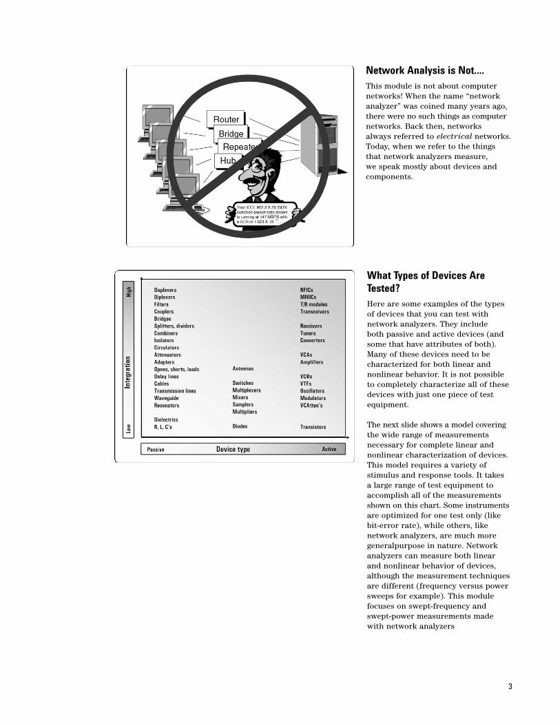
Network Analysis is Not....This module is not about computernetworks! When the name “networkanalyzer” was coined many years ago,there were no such things as computernetworks. Back then, networks always referred to electrical networks.Today, when we refer to the thingsthat network analyzers measure, we speak mostly about devices andcomponents.
What Types of Devices AreTested?Here are some examples of the typesof devices that you can test with network analyzers. They include both passive and active devices (andsome that have attributes of both).Many of these devices need to be characterized for both linear and nonlinear behavior. It is not possibleto completely characterize all of thesedevices with just one piece of testequipment.
The next slide shows a model coveringthe wide range of measurements necessary for complete linear andnonlinear characterization of devices.This model requires a variety of stimulus and response tools. It takes a large range of test equipment toaccomplish all of the measurementsshown on this chart. Some instrumentsare optimized for one test only (likebit-error rate), while others, like network analyzers, are much moregeneralpurpose in nature. Networkanalyzers can measure both linear and nonlinear behavior of devices,although the measurement techniquesare different (frequency versus powersweeps for example). This modulefocuses on swept-frequency andswept-power measurements madewith network analyzers
4
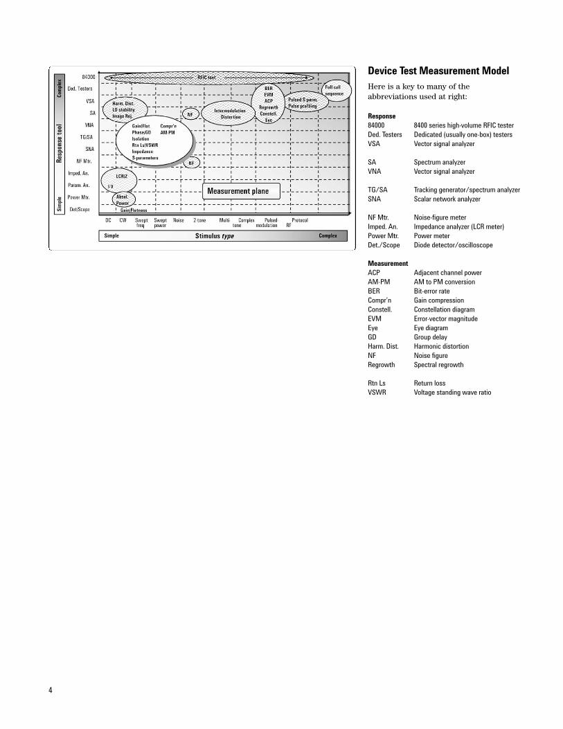
Device Test Measurement ModelHere is a key to many of the abbreviations used at right:
Response84000 8400 series high-volume RFIC testerDed. Testers Dedicated (usually one-box) testersVSA Vector signal analyzer
SA Spectrum analyzerVNA Vector signal analyzer
TG/SA Tracking generator/spectrum analyzerSNA Scalar network analyzer
NF Mtr. Noise-figure meterImped. An. Impedance analyzer (LCR meter)Power Mtr. Power meterDet./Scope Diode detector/oscilloscope
MeasurementACP Adjacent channel powerAM-PM AM to PM conversionBER Bit-error rate Compr’n Gain compressionConstell. Constellation diagramEVM Error-vector magnitudeEye Eye diagramGD Group delayHarm. Dist. Harmonic distortionNF Noise figureRegrowth Spectral regrowth
Rtn Ls Return lossVSWR Voltage standing wave ratio
5
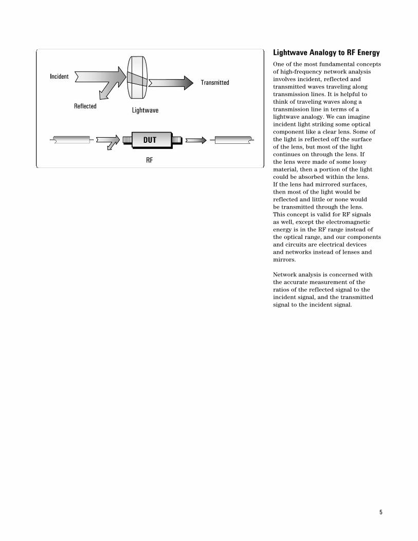
Lightwave Analogy to RF EnergyOne of the most fundamental conceptsof high-frequency network analysisinvolves incident, reflected and transmitted waves traveling alongtransmission lines. It is helpful tothink of traveling waves along a transmission line in terms of a lightwave analogy. We can imagineincident light striking some opticalcomponent like a clear lens. Some ofthe light is reflected off the surface of the lens, but most of the light continues on through the lens. If the lens were made of some lossymaterial, then a portion of the lightcould be absorbed within the lens. If the lens had mirrored surfaces, then most of the light would bereflected and little or none would be transmitted through the lens. This concept is valid for RF signals as well, except the electromagneticenergy is in the RF range instead ofthe optical range, and our componentsand circuits are electrical devices and networks instead of lenses andmirrors.
Network analysis is concerned withthe accurate measurement of theratios of the reflected signal to theincident signal, and the transmittedsignal to the incident signal.
6
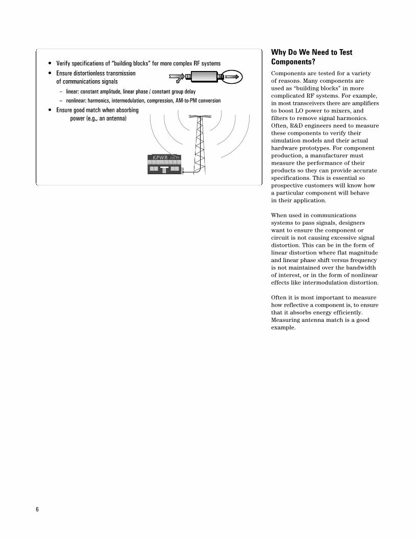
Why Do We Need to TestComponents?Components are tested for a variety of reasons. Many components are used as “building blocks” in morecomplicated RF systems. For example,in most transceivers there are amplifiersto boost LO power to mixers, and filters to remove signal harmonics.Often, R&D engineers need to measurethese components to verify their simulation models and their actualhardware prototypes. For componentproduction, a manufacturer mustmeasure the performance of theirproducts so they can provide accuratespecifications. This is essential soprospective customers will know howa particular component will behave in their application.
When used in communications systems to pass signals, designerswant to ensure the component or circuit is not causing excessive signaldistortion. This can be in the form oflinear distortion where flat magnitudeand linear phase shift versus frequencyis not maintained over the bandwidthof interest, or in the form of nonlineareffects like intermodulation distortion.
Often it is most important to measurehow reflective a component is, to ensurethat it absorbs energy efficiently.Measuring antenna match is a goodexample.
7
AgendaIn this section we will review reflectionand transmission measurements. Wewill see that transmission lines areneeded to convey RF and microwaveenergy from one point to another withminimal loss, that transmission lineshave a characteristic impedance, andthat a termination at the end of atransmission line must match thecharacteristic impedance of the line to prevent loss of energy due to reflections. We will see how the Smith chart simplifies the process of converting reflection data to thecomplex impedance of the termination.For transmission measurements, we will discuss not only simple gainand loss but distortion introduced by linear devices. We will introduce S-parameters and explain why they areused instead of h-, y-, or z-parametersat RF and microwave frequencies.
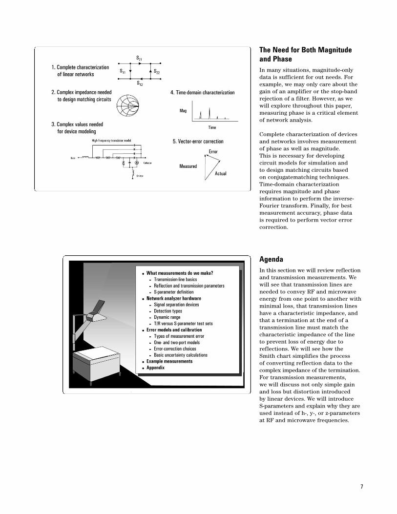
The Need for Both Magnitudeand PhaseIn many situations, magnitude-onlydata is sufficient for out needs. Forexample, we may only care about thegain of an amplifier or the stop-bandrejection of a filter. However, as wewill explore throughout this paper,measuring phase is a critical elementof network analysis.
Complete characterization of devicesand networks involves measurementof phase as well as magnitude. This is necessary for developing circuit models for simulation and to design matching circuits based on conjugatematching techniques.Time-domain characterizationrequires magnitude and phase information to perform the inverse-Fourier transform. Finally, for bestmeasurement accuracy, phase data is required to perform vector errorcorrection.
8
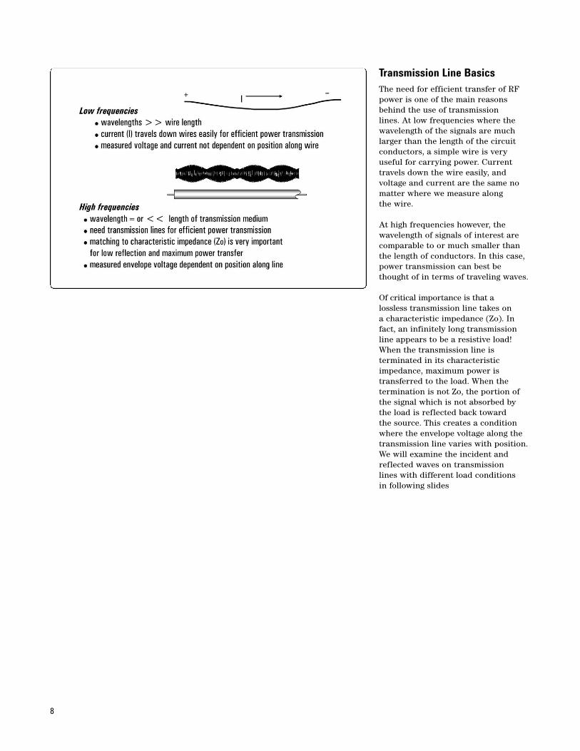
Transmission Line BasicsThe need for efficient transfer of RFpower is one of the main reasonsbehind the use of transmission lines. At low frequencies where thewavelength of the signals are muchlarger than the length of the circuitconductors, a simple wire is very useful for carrying power. Currenttravels down the wire easily, and voltage and current are the same nomatter where we measure along the wire.
At high frequencies however, thewavelength of signals of interest arecomparable to or much smaller thanthe length of conductors. In this case,power transmission can best bethought of in terms of traveling waves.
Of critical importance is that a lossless transmission line takes on a characteristic impedance (Zo). Infact, an infinitely long transmissionline appears to be a resistive load!When the transmission line is terminated in its characteristic impedance, maximum power is transferred to the load. When the termination is not Zo, the portion ofthe signal which is not absorbed bythe load is reflected back toward the source. This creates a conditionwhere the envelope voltage along thetransmission line varies with position.We will examine the incident andreflected waves on transmission lines with different load conditions in following slides
9
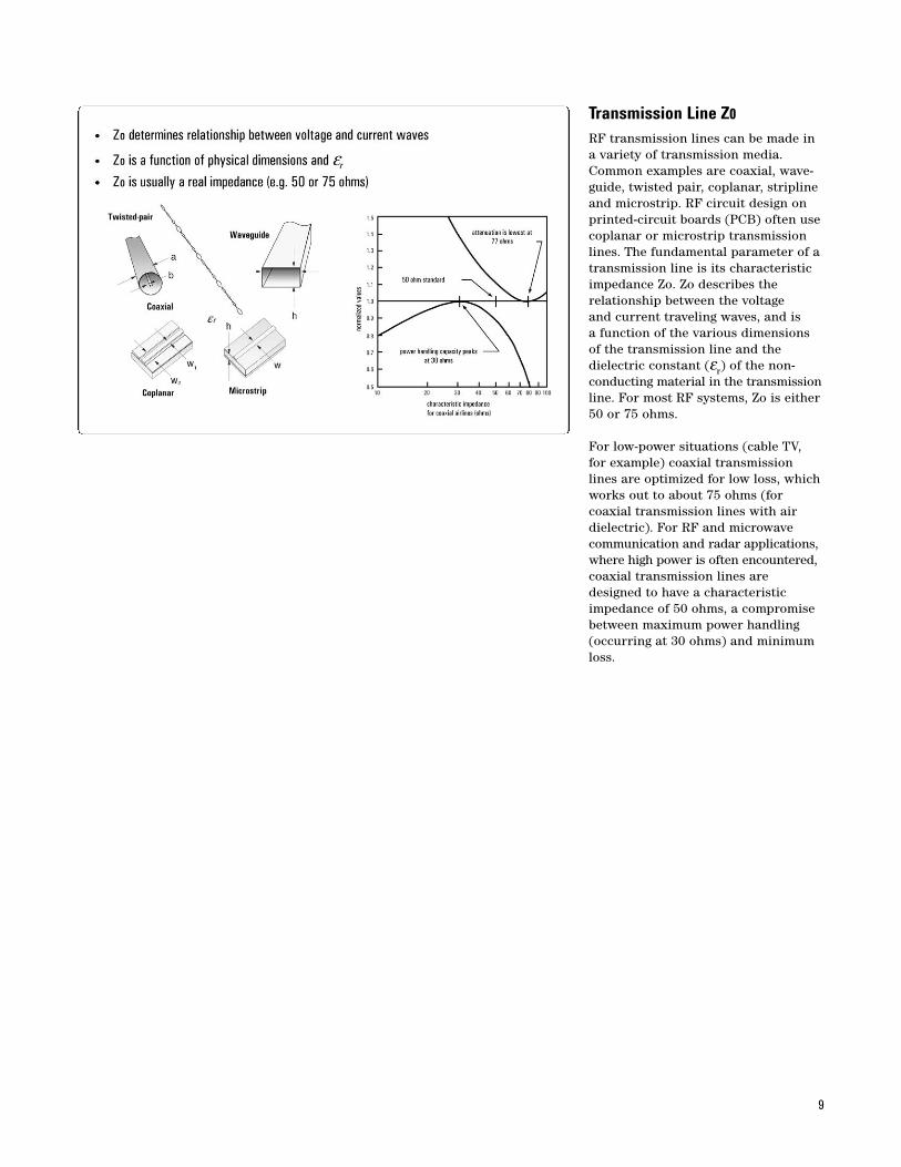
Transmission Line Z0
RF transmission lines can be made ina variety of transmission media.Common examples are coaxial, wave-guide, twisted pair, coplanar, striplineand microstrip. RF circuit design onprinted-circuit boards (PCB) often usecoplanar or microstrip transmissionlines. The fundamental parameter of atransmission line is its characteristicimpedance Zo. Zo describes the relationship between the voltage and current traveling waves, and is a function of the various dimensionsof the transmission line and thedielectric constant (εr) of the non-conducting material in the transmissionline. For most RF systems, Zo is either50 or 75 ohms.
For low-power situations (cable TV, for example) coaxial transmissionlines are optimized for low loss, whichworks out to about 75 ohms (for coaxial transmission lines with airdielectric). For RF and microwavecommunication and radar applications,where high power is often encountered,coaxial transmission lines aredesigned to have a characteristicimpedance of 50 ohms, a compromisebetween maximum power handling(occurring at 30 ohms) and minimumloss.
10
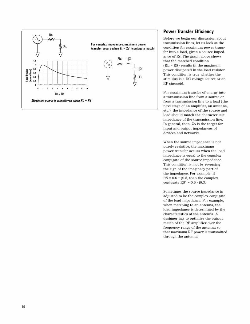
Power Transfer EfficiencyBefore we begin our discussion abouttransmission lines, let us look at thecondition for maximum power trans-fer into a load, given a source imped-ance of Rs. The graph above showsthat the matched condition(RL = RS) results in the maximumpower dissipated in the load resistor.This condition is true whether thestimulus is a DC voltage source or anRF sinusoid.
For maximum transfer of energy intoa transmission line from a source orfrom a transmission line to a load (thenext stage of an amplifier, an antenna,etc.), the impedance of the source andload should match the characteristicimpedance of the transmission line. In general, then, Zo is the target forinput and output impedances ofdevices and networks.
When the source impedance is notpurely resistive, the maximum power transfer occurs when the loadimpedance is equal to the complexconjugate of the source impedance.This condition is met by reversing the sign of the imaginary part of the impedance. For example, if RS = 0.6 + j0.3, then the complex conjugate RS* = 0.6 - j0.3.
Sometimes the source impedance isadjusted to be the complex conjugateof the load impedance. For example,when matching to an antenna, theload impedance is determined by thecharacteristics of the antenna. Adesigner has to optimize the outputmatch of the RF amplifier over the frequency range of the antenna so that maximum RF power is transmittedthrough the antenna
11
Transmission Line TerminatedWith Z0
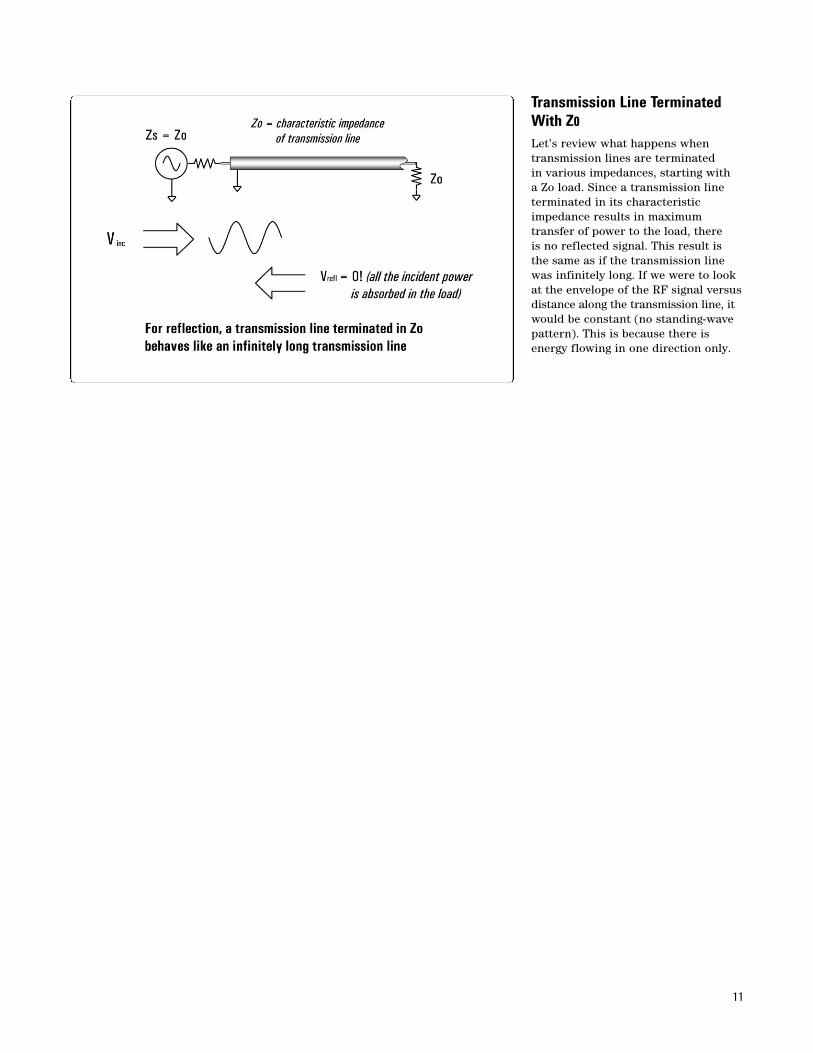
Let’s review what happens whentransmission lines are terminated in various impedances, starting with a Zo load. Since a transmission lineterminated in its characteristic impedance results in maximum transfer of power to the load, there is no reflected signal. This result isthe same as if the transmission linewas infinitely long. If we were to lookat the envelope of the RF signal versusdistance along the transmission line, itwould be constant (no standing-wavepattern). This is because there is energy flowing in one direction only.
12
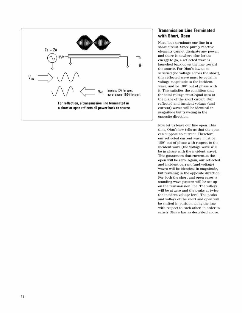
Transmission Line Terminatedwith Short, OpenNext, let’s terminate our line in ashort circuit. Since purely reactive elements cannot dissipate any power,and there is nowhere else for the energy to go, a reflected wave islaunched back down the line towardthe source. For Ohm’s law to be satisfied (no voltage across the short),this reflected wave must be equal involtage magnitude to the incidentwave, and be 180° out of phase withit. This satisfies the condition that the total voltage must equal zero atthe plane of the short circuit. Ourreflected and incident voltage (andcurrent) waves will be identical inmagnitude but traveling in the opposite direction.
Now let us leave our line open. Thistime, Ohm’s law tells us that the opencan support no current. Therefore, our reflected current wave must be180° out of phase with respect to theincident wave (the voltage wave willbe in phase with the incident wave).This guarantees that current at theopen will be zero. Again, our reflectedand incident current (and voltage)waves will be identical in magnitude,but traveling in the opposite direction.For both the short and open cases, astanding-wave pattern will be set upon the transmission line. The valleyswill be at zero and the peaks at twicethe incident voltage level. The peaksand valleys of the short and open willbe shifted in position along the linewith respect to each other, in order tosatisfy Ohm’s law as described above.
13
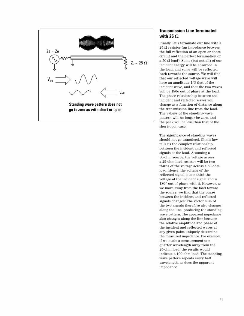
Transmission Line Terminatedwith 25 ΩFinally, let’s terminate our line with a25 Ω resistor (an impedance betweenthe full reflection of an open or shortcircuit and the perfect termination ofa 50 Ω load). Some (but not all) of ourincident energy will be absorbed inthe load, and some will be reflectedback towards the source. We will findthat our reflected voltage wave willhave an amplitude 1/3 that of the incident wave, and that the two waveswill be 180o out of phase at the load.The phase relationship between theincident and reflected waves willchange as a function of distance alongthe transmission line from the load.The valleys of the standing-wave pattern will no longer be zero, and the peak will be less than that of theshort/open case.
The significance of standing wavesshould not go unnoticed. Ohm’s lawtells us the complex relationshipbetween the incident and reflectedsignals at the load. Assuming a 50-ohm source, the voltage across a 25-ohm load resistor will be twothirds of the voltage across a 50-ohmload. Hence, the voltage of the reflected signal is one third the voltage of the incident signal and is180° out of phase with it. However, aswe move away from the load towardthe source, we find that the phasebetween the incident and reflectedsignals changes! The vector sum of the two signals therefore also changesalong the line, producing the standingwave pattern. The apparent impedancealso changes along the line becausethe relative amplitude and phase ofthe incident and reflected waves atany given point uniquely determinethe measured impedance. For example,if we made a measurement one quarter wavelength away from the 25-ohm load, the results would indicate a 100-ohm load. The standingwave pattern repeats every half wavelength, as does the apparentimpedance.
14
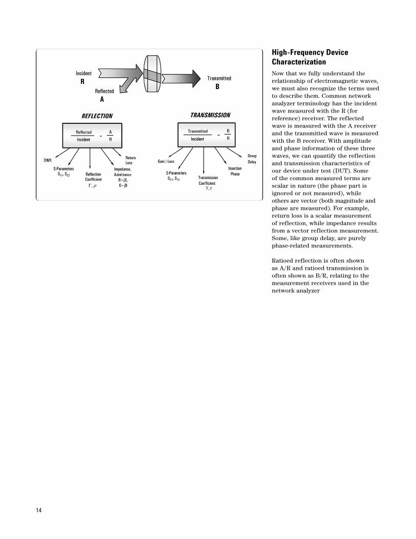
High-Frequency DeviceCharacterizationNow that we fully understand the relationship of electromagnetic waves,we must also recognize the terms usedto describe them. Common networkanalyzer terminology has the incidentwave measured with the R (for reference) receiver. The reflected wave is measured with the A receiverand the transmitted wave is measuredwith the B receiver. With amplitudeand phase information of these threewaves, we can quantify the reflectionand transmission characteristics ofour device under test (DUT). Some of the common measured terms arescalar in nature (the phase part isignored or not measured), while others are vector (both magnitude andphase are measured). For example,return loss is a scalar measurement of reflection, while impedance resultsfrom a vector reflection measurement.Some, like group delay, are purelyphase-related measurements.
Ratioed reflection is often shown as A/R and ratioed transmission isoften shown as B/R, relating to themeasurement receivers used in thenetwork analyzer
15
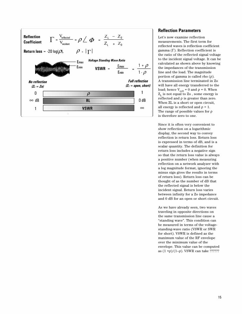
Reflection ParametersLet’s now examine reflection measurements. The first term forreflected waves is reflection coefficientgamma (Γ). Reflection coefficient isthe ratio of the reflected signal voltageto the incident signal voltage. It can becalculated as shown above by knowingthe impedances of the transmissionline and the load. The magnitude portion of gamma is called rho (ρ). A transmission line terminated in Zowill have all energy transferred to theload; hence Vrefl = 0 and ρ = 0. WhenZL is not equal to Zo , some energy isreflected and ρ is greater than zero.When ZL is a short or open circuit, all energy is reflected and ρ = 1. The range of possible values for ρis therefore zero to one.
Since it is often very convenient toshow reflection on a logarithmic display, the second way to conveyreflection is return loss. Return loss is expressed in terms of dB, and is ascalar quantity. The definition forreturn loss includes a negative sign so that the return loss value is alwaysa positive number (when measuringreflection on a network analyzer witha log magnitude format, ignoring theminus sign gives the results in termsof return loss). Return loss can bethought of as the number of dB thatthe reflected signal is below the incident signal. Return loss variesbetween infinity for a Zo impedanceand 0 dB for an open or short circuit.
As we have already seen, two wavestraveling in opposite directions on the same transmission line cause a“standing wave”. This condition can be measured in terms of the voltage-standing-wave ratio (VSWR or SWRfor short). VSWR is defined as themaximum value of the RF envelopeover the minimum value of the envelope. This value can be computedas (1 +ρ)/(1–ρ). VSWR can take ??????
16
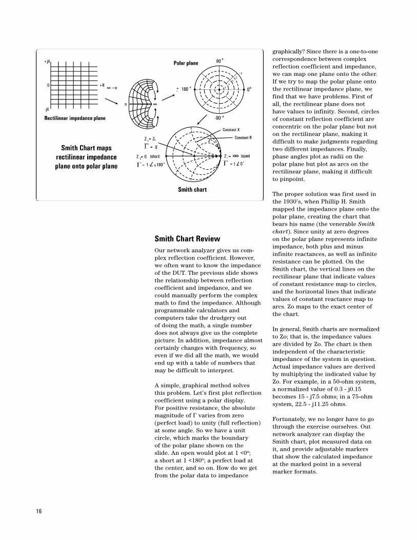
Smith Chart ReviewOur network analyzer gives us com-plex reflection coefficient. However,we often want to know the impedanceof the DUT. The previous slide showsthe relationship between reflectioncoefficient and impedance, and wecould manually perform the complexmath to find the impedance. Althoughprogrammable calculators and computers take the drudgery out of doing the math, a single numberdoes not always give us the completepicture. In addition, impedance almostcertainly changes with frequency, soeven if we did all the math, we wouldend up with a table of numbers thatmay be difficult to interpret.
A simple, graphical method solves this problem. Let’s first plot reflectioncoefficient using a polar display. For positive resistance, the absolutemagnitude of Γ varies from zero (perfect load) to unity (full reflection)at some angle. So we have a unit circle, which marks the boundary of the polar plane shown on the slide. An open would plot at 1 <0o; a short at 1 <180o; a perfect load atthe center, and so on. How do we getfrom the polar data to impedance
graphically? Since there is a one-to-onecorrespondence between complexreflection coefficient and impedance,we can map one plane onto the other.If we try to map the polar plane ontothe rectilinear impedance plane, wefind that we have problems. First ofall, the rectilinear plane does not have values to infinity. Second, circlesof constant reflection coefficient areconcentric on the polar plane but noton the rectilinear plane, making it difficult to make judgments regardingtwo different impedances. Finally,phase angles plot as radii on the polar plane but plot as arcs on the rectilinear plane, making it difficult to pinpoint.
The proper solution was first used inthe 1930’s, when Phillip H. Smithmapped the impedance plane onto thepolar plane, creating the chart thatbears his name (the venerable Smithchart). Since unity at zero degrees on the polar plane represents infiniteimpedance, both plus and minus infinite reactances, as well as infiniteresistance can be plotted. On theSmith chart, the vertical lines on therectilinear plane that indicate valuesof constant resistance map to circles,and the horizontal lines that indicatevalues of constant reactance map toarcs. Zo maps to the exact center ofthe chart.
In general, Smith charts are normalizedto Zo; that is, the impedance valuesare divided by Zo. The chart is thenindependent of the characteristicimpedance of the system in question.Actual impedance values are derivedby multiplying the indicated value byZo. For example, in a 50-ohm system,a normalized value of 0.3 - j0.15becomes 15 - j7.5 ohms; in a 75-ohmsystem, 22.5 - j11.25 ohms.
Fortunately, we no longer have to gothrough the exercise ourselves. Outnetwork analyzer can display theSmith chart, plot measured data on it, and provide adjustable markersthat show the calculated impedance at the marked point in a several marker formats.
17
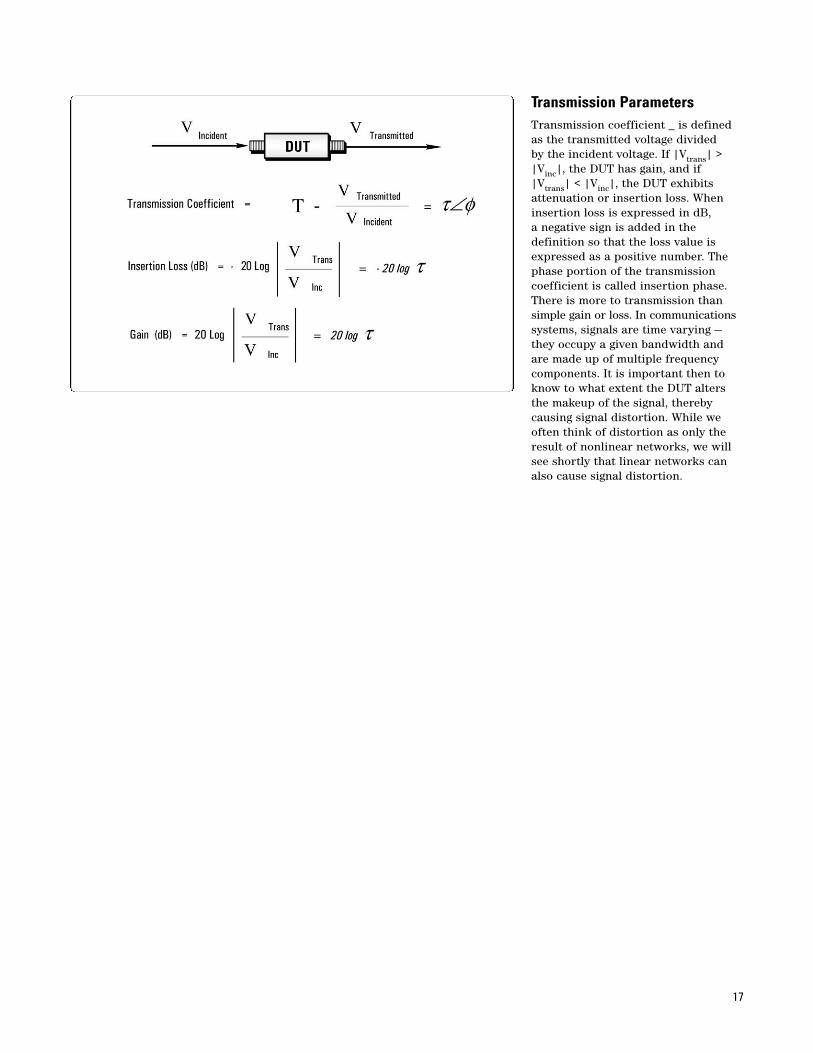
Transmission ParametersTransmission coefficient _ is definedas the transmitted voltage divided by the incident voltage. If |Vtrans| >|Vinc|, the DUT has gain, and if |Vtrans| < |Vinc|, the DUT exhibitsattenuation or insertion loss. Wheninsertion loss is expressed in dB, a negative sign is added in the definition so that the loss value isexpressed as a positive number. Thephase portion of the transmissioncoefficient is called insertion phase.There is more to transmission thansimple gain or loss. In communicationssystems, signals are time varying —they occupy a given bandwidth andare made up of multiple frequencycomponents. It is important then toknow to what extent the DUT altersthe makeup of the signal, therebycausing signal distortion. While weoften think of distortion as only theresult of nonlinear networks, we willsee shortly that linear networks canalso cause signal distortion.
18
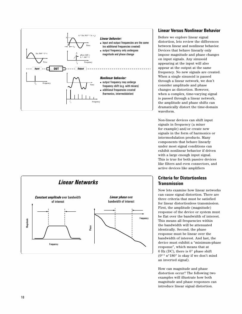
Linear Versus Nonlinear BehaviorBefore we explore linear signal distortion, lets review the differencesbetween linear and nonlinear behavior.Devices that behave linearly onlyimpose magnitude and phase changeson input signals. Any sinusoid appearing at the input will alsoappear at the output at the same frequency. No new signals are created.When a single sinusoid is passedthrough a linear network, we don’tconsider amplitude and phase changes as distortion. However, when a complex, time-varying signal is passed through a linear network,the amplitude and phase shifts candramatically distort the time-domainwaveform.
Non-linear devices can shift input signals in frequency (a mixer for example) and/or create new signals in the form of harmonics orintermodulation products. Many components that behave linearlyunder most signal conditions canexhibit nonlinear behavior if drivenwith a large enough input signal. This is true for both passive deviceslike filters and even connectors, andactive devices like amplifiers
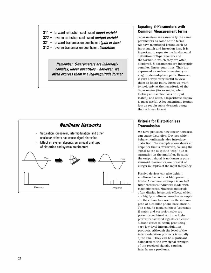
Criteria for DistortionlessTransmissionNow lets examine how linear networkscan cause signal distortion. There arethree criteria that must be satisfiedfor linear distortionless transmission.First, the amplitude (magnitude)response of the device or system mustbe flat over the bandwidth of interest.This means all frequencies within the bandwidth will be attenuatedidentically. Second, the phaseresponse must be linear over thebandwidth of interest. And last, thedevice must exhibit a “minimum-phaseresponse”, which means that at 0 Hz (DC), there is 0° phase shift(0o ± n*180° is okay if we don’t mindan inverted signal).
How can magnitude and phase distortion occur? The following twoexamples will illustrate how both magnitude and phase responses canintroduce linear signal distortion.
19
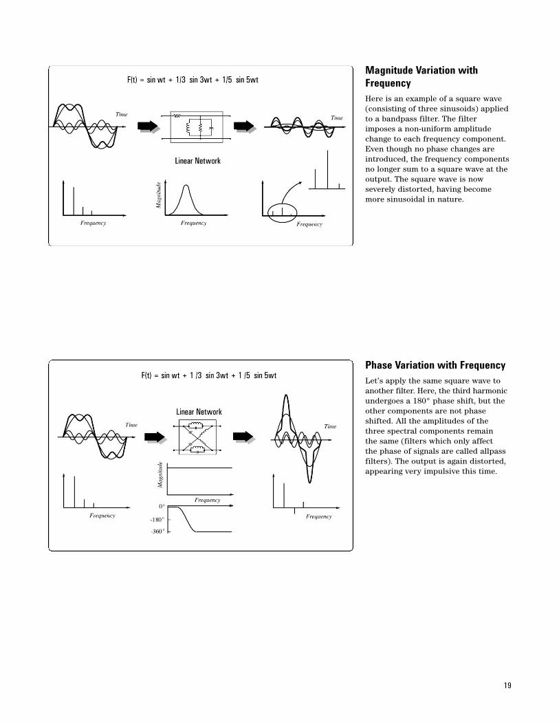
Phase Variation with FrequencyLet’s apply the same square wave toanother filter. Here, the third harmonicundergoes a 180° phase shift, but theother components are not phase shifted. All the amplitudes of the three spectral components remain the same (filters which only affect the phase of signals are called allpassfilters). The output is again distorted,appearing very impulsive this time.
Magnitude Variation withFrequencyHere is an example of a square wave(consisting of three sinusoids) appliedto a bandpass filter. The filter imposes a non-uniform amplitudechange to each frequency component.Even though no phase changes areintroduced, the frequency componentsno longer sum to a square wave at theoutput. The square wave is nowseverely distorted, having becomemore sinusoidal in nature.
20
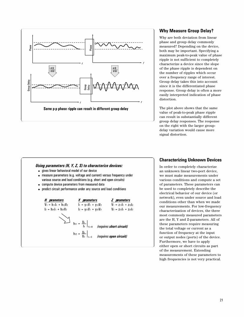
Group DelayAnother useful measure of phase distortion is group delay. Group delayis a measure of the transit time of asignal through the device under test,versus frequency. Group delay is calculated by differentiating the insertionphase response of the DUTversus frequency. Another way to saythis is that group delay is a measureof the slope of the transmission phaseresponse. The linear portion of thephase response is converted to a constant value (representing the averagesignal-transit time) and deviationsfrom linear phase are transformedinto deviations from constant groupdelay. The variations in group delaycause signal distortion, just as deviations from linear phase causedistortion. Group delay is just anotherway to look at linear phase distortion.
When specifying or measuring groupdelay, it is important to quantify theaperture in which the measurement ismade. The aperture is defined as thefrequency delta used in the differenti-ation process (the denominator in thegroup-delay formula). As we widen theaperture, trace noise is reduced butless group-delay resolution is available (we are essentially averaging thephase response over a wider window).As we make the aperture more narrow, trace noise increases but wehave more measurement resolution.
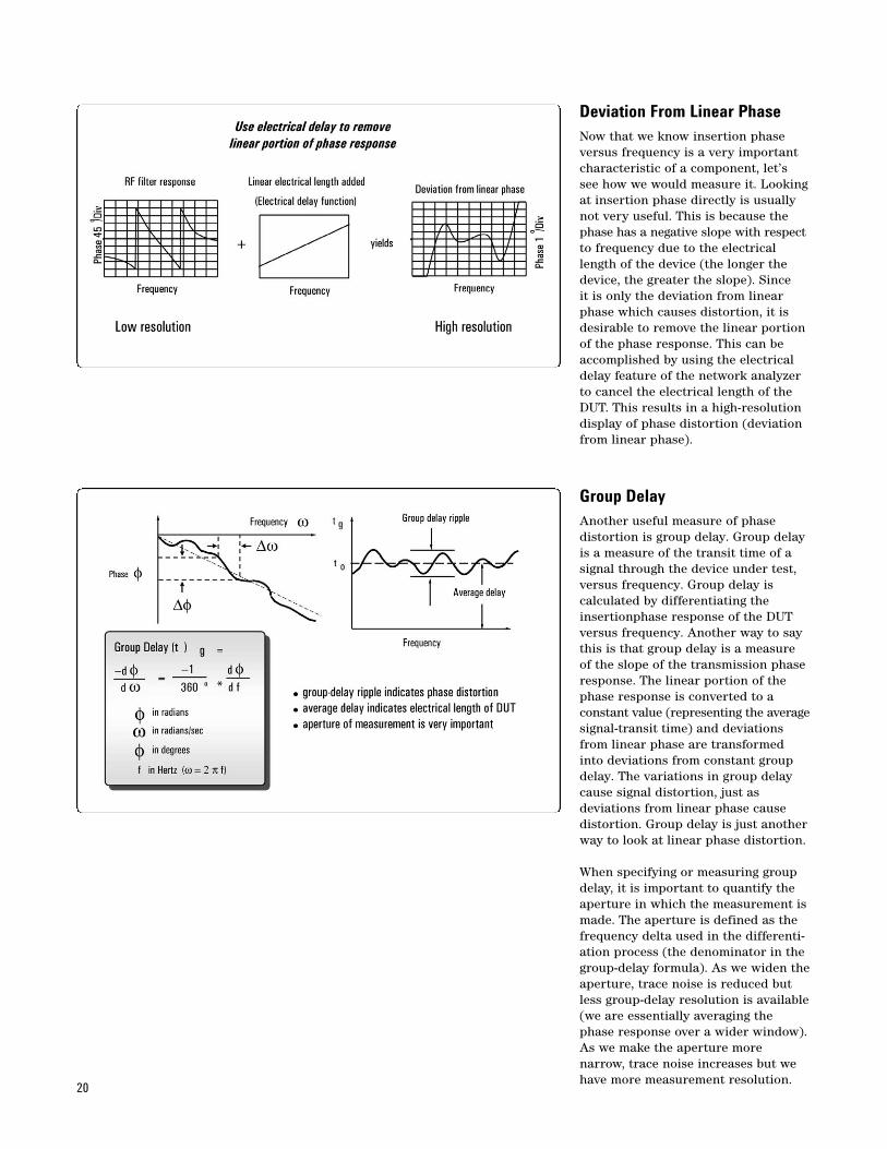
Deviation From Linear PhaseNow that we know insertion phaseversus frequency is a very importantcharacteristic of a component, let’ssee how we would measure it. Lookingat insertion phase directly is usuallynot very useful. This is because thephase has a negative slope with respectto frequency due to the electricallength of the device (the longer thedevice, the greater the slope). Since it is only the deviation from linearphase which causes distortion, it isdesirable to remove the linear portionof the phase response. This can beaccomplished by using the electricaldelay feature of the network analyzerto cancel the electrical length of theDUT. This results in a high-resolutiondisplay of phase distortion (deviationfrom linear phase).
21
Characterizing Unknown DevicesIn order to completely characterize an unknown linear two-port device,we must make measurements undervarious conditions and compute a setof parameters. These parameters canbe used to completely describe theelectrical behavior of our device (ornetwork), even under source and loadconditions other than when we madeour measurements. For low-frequencycharacterization of devices, the threemost commonly measured parametersare the H, Y and Z-parameters. All ofthese parameters require measuringthe total voltage or current as a function of frequency at the input or output nodes (ports) of the device.Furthermore, we have to apply either open or short circuits as part of the measurement. Extending measurements of these parameters tohigh frequencies is not very practical.
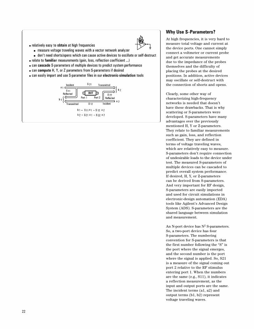
Why Measure Group Delay?Why are both deviation from linearphase and group delay commonlymeasured? Depending on the device,both may be important. Specifying amaximum peak-to-peak value of phaseripple is not sufficient to completelycharacterize a device since the slopeof the phase ripple is dependent onthe number of ripples which occurover a frequency range of interest.Group delay takes this into accountsince it is the differentiated phaseresponse. Group delay is often a moreeasily interpreted indication of phasedistortion.
The plot above shows that the samevalue of peak-to-peak phase ripple can result in substantially differentgroup delay responses. The responseon the right with the larger group-delay variation would cause more signal distortion.
22
Why Use S-Parameters?At high frequencies, it is very hard tomeasure total voltage and current atthe device ports. One cannot simplyconnect a voltmeter or current probeand get accurate measurements due to the impedance of the probesthemselves and the difficulty of placing the probes at the desired positions. In addition, active devicesmay oscillate or self-destruct with the connection of shorts and opens.
Clearly, some other way of characterizing high-frequency networks is needed that doesn’t have these drawbacks. That is whyscattering or S-parameters were developed. S-parameters have manyadvantages over the previously mentioned H, Y or Z-parameters. They relate to familiar measurementssuch as gain, loss, and reflection coefficient. They are defined in terms of voltage traveling waves,which are relatively easy to measure.S-parameters don’t require connectionof undesirable loads to the device undertest. The measured S-parameters ofmultiple devices can be cascaded topredict overall system performance. If desired, H, Y, or Z-parameters can be derived from S-parameters.And very important for RF design, S-parameters are easily imported and used for circuit simulations inelectronic-design automation (EDA)tools like Agilent’s Advanced DesignSystem (ADS). S-parameters are theshared language between simulationand measurement.
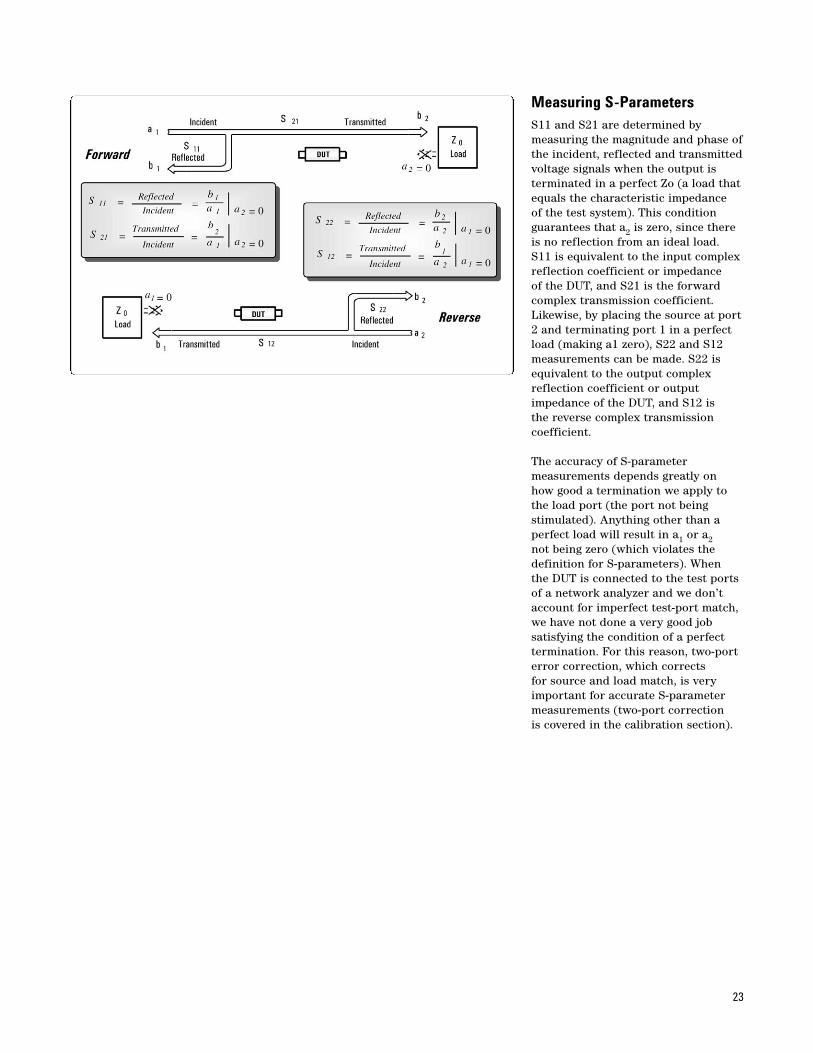
An N-port device has N2 S-parameters.So, a two-port device has four S-parameters. The numbering convention for S-parameters is thatthe first number following the “S” isthe port where the signal emerges,and the second number is the portwhere the signal is applied. So, S21 is a measure of the signal coming outport 2 relative to the RF stimulusentering port 1. When the numbersare the same (e.g., S11), it indicates a reflection measurement, as the input and output ports are the same.The incident terms (a1, a2) and output terms (b1, b2) represent voltage traveling waves.
23
Measuring S-ParametersS11 and S21 are determined by measuring the magnitude and phase ofthe incident, reflected and transmittedvoltage signals when the output is terminated in a perfect Zo (a load thatequals the characteristic impedance of the test system). This conditionguarantees that a2 is zero, since thereis no reflection from an ideal load.S11 is equivalent to the input complexreflection coefficient or impedance of the DUT, and S21 is the forwardcomplex transmission coefficient. Likewise, by placing the source at port2 and terminating port 1 in a perfectload (making a1 zero), S22 and S12measurements can be made. S22 isequivalent to the output complexreflection coefficient or output impedance of the DUT, and S12 is the reverse complex transmissioncoefficient.
The accuracy of S-parameter measurements depends greatly onhow good a termination we apply tothe load port (the port not being stimulated). Anything other than aperfect load will result in a1 or a2not being zero (which violates the definition for S-parameters). When the DUT is connected to the test portsof a network analyzer and we don’taccount for imperfect test-port match,we have not done a very good job satisfying the condition of a perfecttermination. For this reason, two-porterror correction, which corrects for source and load match, is veryimportant for accurate S-parametermeasurements (two-port correction is covered in the calibration section).
24
Criteria for DistortionlessTransmissionWe have just seen how linear networkscan cause distortion. Devices whichbehave nonlinearly also introduce distortion. The example above shows anamplifier that is overdriven, causing thesignal at the output to “clip” due tosaturation in the amplifier. Becausethe output signal is no longer a puresinusoid, harmonics are present atinteger multiples of the input frequency.
Passive devices can also exhibit nonlinear behavior at high power levels. A common example is an L-Cfilter that uses inductors made withmagnetic cores. Magnetic materialsoften display hysteresis effects, whichare highly nonlinear. Another exampleare the connectors used in the antennapath of a cellular-phone base station.The metal-to-metal contacts (especiallyif water and corrosion salts are present) combined with the high-power transmitted signals can cause a diode effect to occur, producing very low-level intermodulation products. Although the level of theintermodulation products is usuallyquite small, they can be significantcompared to the low signal strength of the received signals, causing interference problems.
Equating S-Parameters withCommon Measurement TermsS-parameters are essentially the sameparameters as some of the terms we have mentioned before, such asinput match and insertion loss. It isimportant to separate the fundamentaldefinition of S-parameters and the format in which they are often displayed. S-parameters are inherentlycomplex, linear quantities. They areexpressed as real-and-imaginary ormagnitude-and-phase pairs. However,it isn’t always very useful to viewthem as linear pairs. Often we want to look only at the magnitude of the S-parameter (for example, when looking at insertion loss or inputmatch), and often, a logarithmic displayis most useful. A log-magnitude formatlets us see far more dynamic rangethan a linear format.
25
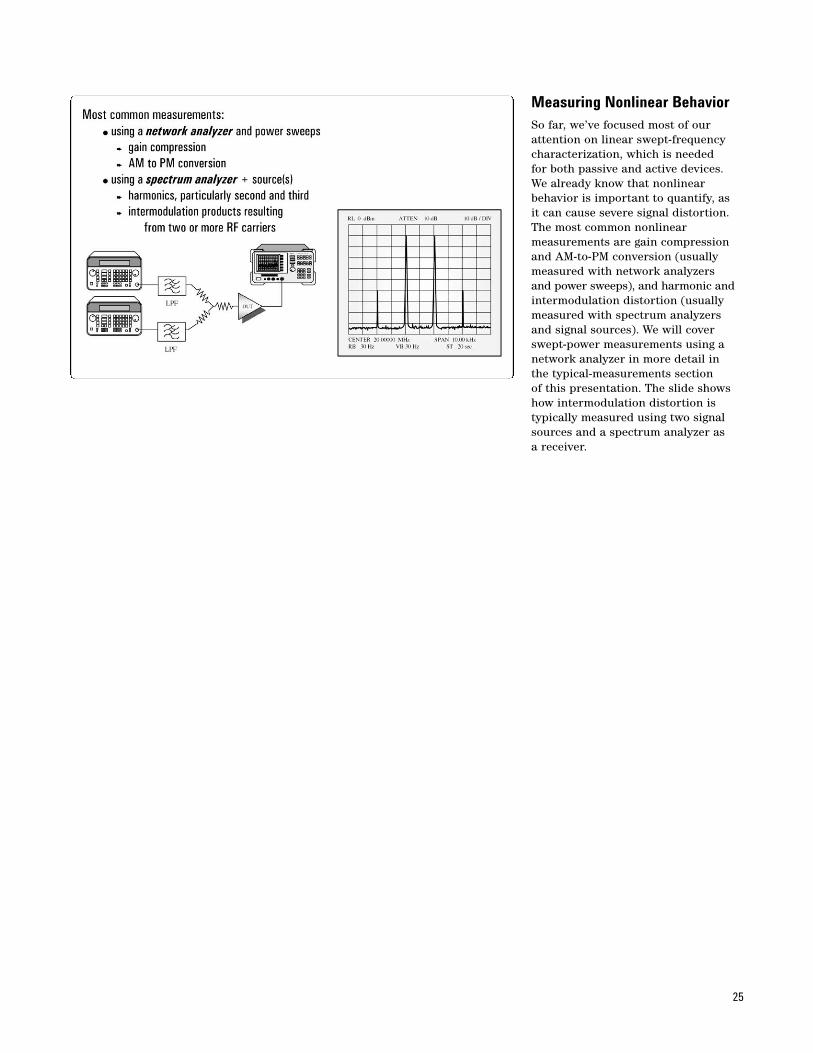
Measuring Nonlinear BehaviorSo far, we’ve focused most of ourattention on linear swept-frequencycharacterization, which is needed for both passive and active devices.We already know that nonlinearbehavior is important to quantify, as it can cause severe signal distortion.The most common nonlinear measurements are gain compressionand AM-to-PM conversion (usuallymeasured with network analyzers and power sweeps), and harmonic andintermodulation distortion (usuallymeasured with spectrum analyzersand signal sources). We will coverswept-power measurements using anetwork analyzer in more detail in the typical-measurements section of this presentation. The slide showshow intermodulation distortion is typically measured using two signalsources and a spectrum analyzer as a receiver.
26
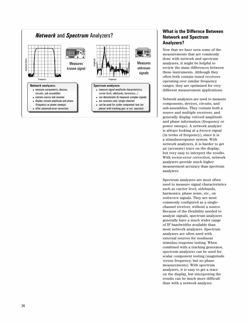
What is the Differnce BetweenNetwork and SpectrumAnalyzers?Now that we have seen some of themeasurements that are commonlydone with network and spectrum analyzers, it might be helpful toreview the main differences betweenthese instruments. Although theyoften both contain tuned receiversoperating over similar frequencyranges, they are optimized for verydifferent measurement applications.
Network analyzers are used to measurecomponents, devices, circuits, andsub-assemblies. They contain both asource and multiple receivers, andgenerally display ratioed amplitudeand phase information (frequency orpower sweeps). A network analyzer is always looking at a known signal (in terms of frequency), since it is a stimulusresponse system. With network analyzers, it is harder to getan (accurate) trace on the display, but very easy to interpret the results.With vector-error correction, networkanalyzers provide much higher measurement accuracy than spectrumanalyzers.
Spectrum analyzers are most oftenused to measure signal characteristicssuch as carrier level, sidebands, harmonics, phase noise, etc., onunknown signals. They are most commonly configured as a single-channel receiver, without a source.Because of the flexibility needed toanalyze signals, spectrum analyzersgenerally have a much wider range of IF bandwidths available than most network analyzers. Spectrumanalyzers are often used with external sources for nonlinear stimulus/response testing. When combined with a tracking generator,spectrum analyzers can be used forscalar component testing (magnitudeversus frequency, but no phase measurements). With spectrum analyzers, it is easy to get a trace on the display, but interpreting theresults can be much more difficultthan with a network analyzer.
27
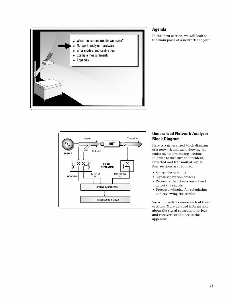
Generalized Network AnalyzerBlock DiagramHere is a generalized block diagram of a network analyzer, showing themajor signal-processing sections. In order to measure the incident,reflected and transmitted signal, four sections are required:
• Source for stimulus• Signal-separation devices• Receivers that downconvert and
detect the signals• Processor/display for calculating
and reviewing the results
We will briefly examine each of thesesections. More detailed informationabout the signal separation devicesand receiver section are in the appendix.
AgendaIn this next section, we will look atthe main parts of a network analyzer.
28
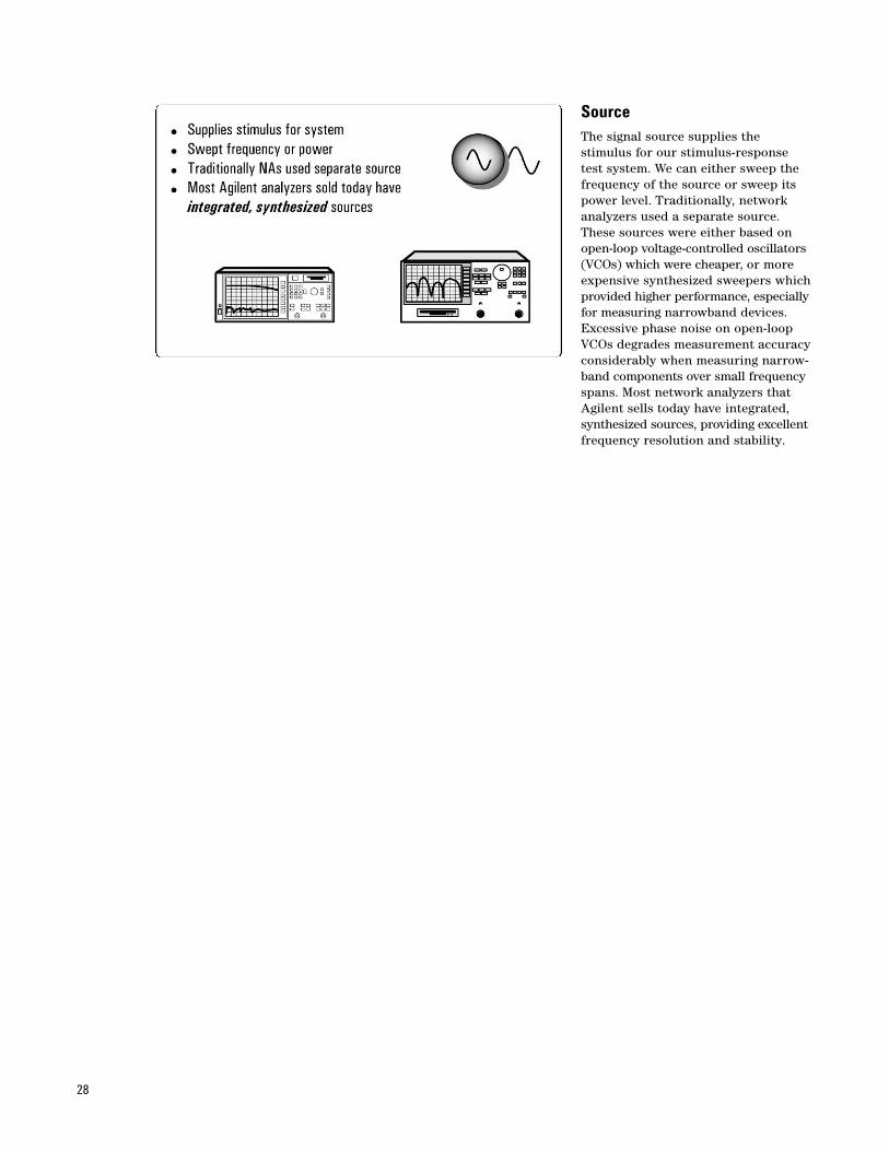
SourceThe signal source supplies the stimulus for our stimulus-responsetest system. We can either sweep thefrequency of the source or sweep itspower level. Traditionally, networkanalyzers used a separate source.These sources were either based onopen-loop voltage-controlled oscillators(VCOs) which were cheaper, or moreexpensive synthesized sweepers whichprovided higher performance, especiallyfor measuring narrowband devices.Excessive phase noise on open-loopVCOs degrades measurement accuracyconsiderably when measuring narrow-band components over small frequencyspans. Most network analyzers thatAgilent sells today have integrated,synthesized sources, providing excellentfrequency resolution and stability.
29
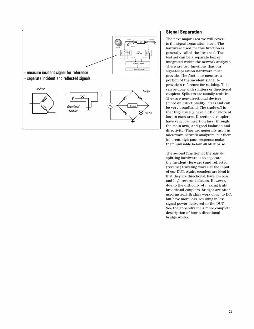
Signal SeparationThe next major area we will cover is the signal separation block. Thehardware used for this function isgenerally called the “test set”. The test set can be a separate box or integrated within the network analyzer.There are two functions that our signal-separation hardware must provide. The first is to measure a portion of the incident signal to provide a reference for ratioing. Thiscan be done with splitters or directionalcouplers. Splitters are usually resistive.They are non-directional devices(more on directionality later) and canbe very broadband. The trade-off isthat they usually have 6 dB or more of loss in each arm. Directional couplershave very low insertion loss (throughthe main arm) and good isolation anddirectivity. They are generally used inmicrowave network analyzers, but theirinherent high-pass response makesthem unusable below 40 MHz or so.
The second function of the signal-splitting hardware is to separate the incident (forward) and reflected(reverse) traveling waves at the inputof our DUT. Again, couplers are ideal inthat they are directional, have low loss,and high reverse isolation. However, due to the difficulty of making trulybroadband couplers, bridges are oftenused instead. Bridges work down to DC,but have more loss, resulting in lesssignal power delivered to the DUT. See the appendix for a more completedescription of how a directionalbridge works.
30
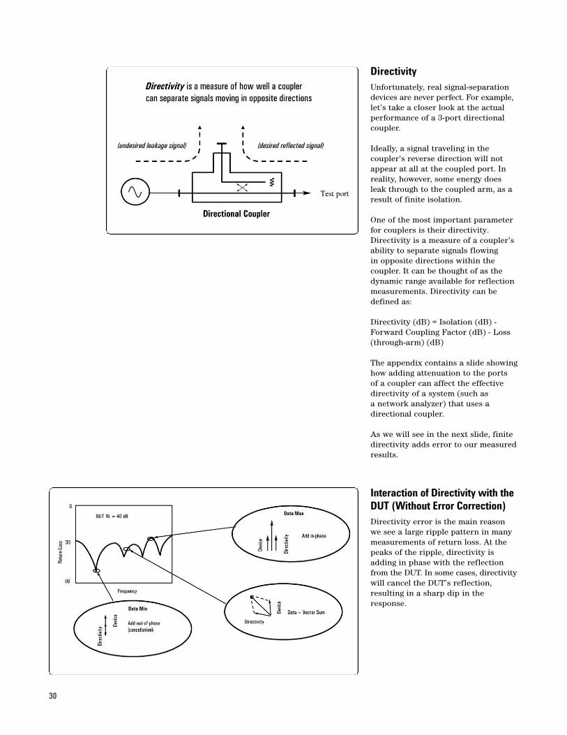
Interaction of Directivity with theDUT (Without Error Correction)Directivity error is the main reasonwe see a large ripple pattern in manymeasurements of return loss. At thepeaks of the ripple, directivity isadding in phase with the reflectionfrom the DUT. In some cases, directivitywill cancel the DUT’s reflection,resulting in a sharp dip in theresponse.
DirectivityUnfortunately, real signal-separationdevices are never perfect. For example,let’s take a closer look at the actualperformance of a 3-port directionalcoupler.
Ideally, a signal traveling in the coupler’s reverse direction will notappear at all at the coupled port. Inreality, however, some energy doesleak through to the coupled arm, as aresult of finite isolation.
One of the most important parameterfor couplers is their directivity.Directivity is a measure of a coupler’sability to separate signals flowing in opposite directions within the coupler. It can be thought of as thedynamic range available for reflectionmeasurements. Directivity can bedefined as:
Directivity (dB) = Isolation (dB) -Forward Coupling Factor (dB) - Loss(through-arm) (dB)
The appendix contains a slide showinghow adding attenuation to the ports of a coupler can affect the effectivedirectivity of a system (such as a network analyzer) that uses a directional coupler.
As we will see in the next slide, finitedirectivity adds error to our measuredresults.
31
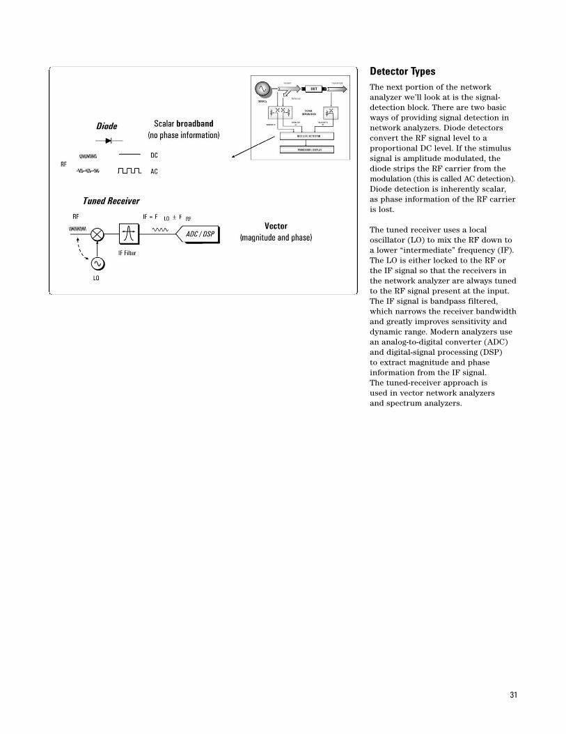
Detector TypesThe next portion of the network analyzer we’ll look at is the signal-detection block. There are two basicways of providing signal detection innetwork analyzers. Diode detectorsconvert the RF signal level to a proportional DC level. If the stimulussignal is amplitude modulated, thediode strips the RF carrier from themodulation (this is called AC detection).Diode detection is inherently scalar, as phase information of the RF carrieris lost.
The tuned receiver uses a local oscillator (LO) to mix the RF down toa lower “intermediate” frequency (IF).The LO is either locked to the RF orthe IF signal so that the receivers inthe network analyzer are always tunedto the RF signal present at the input.The IF signal is bandpass filtered,which narrows the receiver bandwidthand greatly improves sensitivity anddynamic range. Modern analyzers usean analog-to-digital converter (ADC)and digital-signal processing (DSP) to extract magnitude and phase information from the IF signal. The tuned-receiver approach is used in vector network analyzers and spectrum analyzers.
32
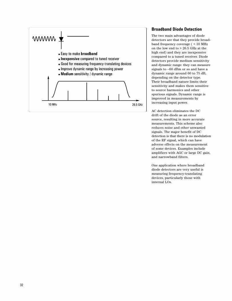
Broadband Diode DetectionThe two main advantages of diodedetectors are that they provide broad-band frequency coverage ( < 10 MHzon the low end to > 26.5 GHz at thehigh end) and they are inexpensivecompared to a tuned receiver. Diodedetectors provide medium sensitivityand dynamic range: they can measuresignals to –60 dBm or so and have adynamic range around 60 to 75 dB,depending on the detector type. Their broadband nature limits theirsensitivity and makes them sensitiveto source harmonics and other spurious signals. Dynamic range isimproved in measurements by increasing input power.
AC detection eliminates the DC drift of the diode as an error source, resulting in more accuratemeasurements. This scheme alsoreduces noise and other unwanted signals. The major benefit of DC detection is that there is no modulationof the RF signal, which can haveadverse effects on the measurement of some devices. Examples includeamplifiers with AGC or large DC gain,and narrowband filters.
One application where broadbanddiode detectors are very useful ismeasuring frequency-translatingdevices, particularly those with internal LOs.
33
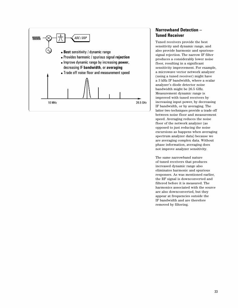
Narrowband Detection – Tuned ReceiverTuned receivers provide the best sensitivity and dynamic range, andalso provide harmonic and spurious-signal rejection. The narrow IF filterproduces a considerably lower noisefloor, resulting in a significant sensitivity improvement. For example,a microwave vector network analyzer(using a tuned receiver) might have a 3 kHz IF bandwidth, where a scalaranalyzer’s diode detector noise bandwidth might be 26.5 GHz.Measurement dynamic range isimproved with tuned receivers byincreasing input power, by decreasingIF bandwidth, or by averaging. The latter two techniques provide a trade offbetween noise floor and measurementspeed. Averaging reduces the noisefloor of the network analyzer (asopposed to just reducing the noiseexcursions as happens when averagingspectrum analyzer data) because weare averaging complex data. Withoutphase information, averaging does not improve analyzer sensitivity.
The same narrowband nature of tuned receivers that producesincreased dynamic range also eliminates harmonic and spuriousresponses. As was mentioned earlier,the RF signal is downconverted andfiltered before it is measured. The harmonics associated with the sourceare also downconverted, but theyappear at frequencies outside the IF bandwidth and are thereforeremoved by filtering.
34
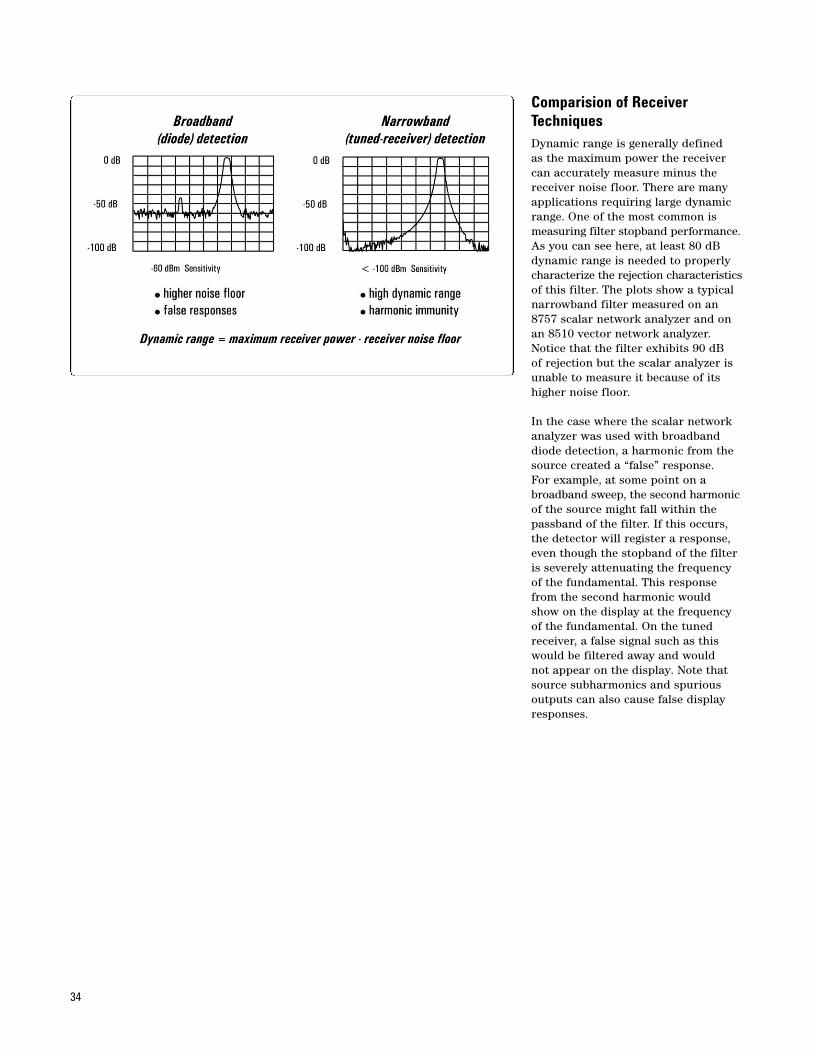
Comparision of ReceiverTechniquesDynamic range is generally defined as the maximum power the receivercan accurately measure minus thereceiver noise floor. There are manyapplications requiring large dynamicrange. One of the most common ismeasuring filter stopband performance.As you can see here, at least 80 dBdynamic range is needed to properlycharacterize the rejection characteristicsof this filter. The plots show a typicalnarrowband filter measured on an8757 scalar network analyzer and onan 8510 vector network analyzer.Notice that the filter exhibits 90 dB of rejection but the scalar analyzer isunable to measure it because of itshigher noise floor.
In the case where the scalar networkanalyzer was used with broadbanddiode detection, a harmonic from thesource created a “false” response. For example, at some point on abroadband sweep, the second harmonicof the source might fall within thepassband of the filter. If this occurs,the detector will register a response,even though the stopband of the filteris severely attenuating the frequencyof the fundamental. This responsefrom the second harmonic would show on the display at the frequencyof the fundamental. On the tunedreceiver, a false signal such as thiswould be filtered away and would not appear on the display. Note thatsource subharmonics and spuriousoutputs can also cause false displayresponses.
35
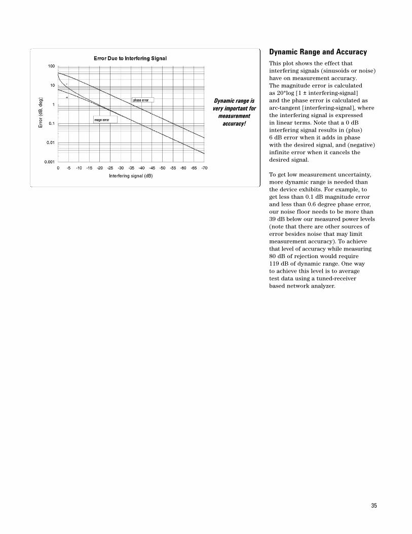
Dynamic Range and AccuracyThis plot shows the effect that interfering signals (sinusoids or noise)have on measurement accuracy. The magnitude error is calculated as 20*log [1 ± interfering-signal] and the phase error is calculated asarc-tangent [interfering-signal], wherethe interfering signal is expressed in linear terms. Note that a 0 dB interfering signal results in (plus) 6 dB error when it adds in phase with the desired signal, and (negative)infinite error when it cancels thedesired signal.
To get low measurement uncertainty,more dynamic range is needed thanthe device exhibits. For example, toget less than 0.1 dB magnitude errorand less than 0.6 degree phase error,our noise floor needs to be more than39 dB below our measured power levels(note that there are other sources oferror besides noise that may limitmeasurement accuracy). To achievethat level of accuracy while measuring80 dB of rejection would require 119 dB of dynamic range. One way to achieve this level is to average test data using a tuned-receiver based network analyzer.
36
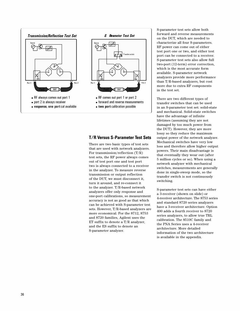
T/R Versus S-Parameter Test SetsThere are two basic types of test setsthat are used with network analyzers.For transmission/reflection (T/R) test sets, the RF power always comesout of test port one and test port two is always connected to a receiverin the analyzer. To measure reversetransmission or output reflection of the DUT, we must disconnect it,turn it around, and re-connect it to the analyzer. T/R-based networkanalyzers offer only response and one-port calibrations, so measurementaccuracy is not as good as that whichcan be achieved with S-parameter testsets. However, T/R-based analyzers aremore economical. For the 8712, 8753and 8720 families, Agilent uses the ET suffix to denote a T/R analyzer,and the ES suffix to denote an S-parameter analyzer.
S-parameter test sets allow both forward and reverse measurements on the DUT, which are needed to characterize all four S-parameters. RF power can come out of either test port one or two, and either testport can be connected to a receiver. S-parameter test sets also allow fulltwo-port (12-term) error correction,which is the most accurate form available. S-parameter network analyzers provide more performancethan T/R-based analyzers, but costmore due to extra RF components in the test set.
There are two different types of transfer switches that can be used in an S-parameter test set: solid-stateand mechanical. Solid-state switcheshave the advantage of infinite lifetimes (assuming they are not damaged by too much power from the DUT). However, they are morelossy so they reduce the maximumoutput power of the network analyzer.Mechanical switches have very lowloss and therefore allow higher outputpowers. Their main disadvantage isthat eventually they wear out (after 5 million cycles or so). When using anetwork analyzer with mechanicalswitches, measurements are generallydone in single-sweep mode, so thetransfer switch is not continuouslyswitching.
S-parameter test sets can have either a 3-receiver (shown on slide) or 4-receiver architecture. The 8753 seriesand standard 8720 series analyzershave a 3-receiver architecture. Option400 adds a fourth receiver to 8720series analyzers, to allow true TRL calibration. The 8510C family and the PNA Series uses a 4-receiver architecture. More detailed information of the two architecture is available in the appendix.
37
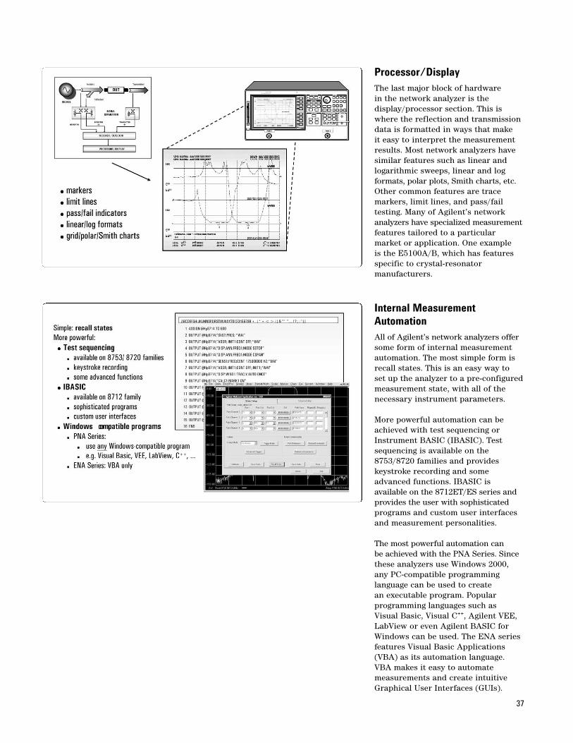
Internal MeasurementAutomationAll of Agilent’s network analyzers offersome form of internal measurementautomation. The most simple form isrecall states. This is an easy way to set up the analyzer to a pre-configuredmeasurement state, with all of thenecessary instrument parameters.
More powerful automation can beachieved with test sequencing orInstrument BASIC (IBASIC). Testsequencing is available on the8753/8720 families and provides keystroke recording and someadvanced functions. IBASIC is available on the 8712ET/ES series andprovides the user with sophisticatedprograms and custom user interfacesand measurement personalities.
The most powerful automation can be achieved with the PNA Series. Sincethese analyzers use Windows 2000,any PC-compatible programming language can be used to create an executable program. Popular programming languages such as Visual Basic, Visual C++, Agilent VEE,LabView or even Agilent BASIC forWindows can be used. The ENA seriesfeatures Visual Basic Applications(VBA) as its automation language.VBA makes it easy to automate measurements and create intuitiveGraphical User Interfaces (GUIs).
Processor/DisplayThe last major block of hardware in the network analyzer is the display/processor section. This iswhere the reflection and transmissiondata is formatted in ways that make it easy to interpret the measurementresults. Most network analyzers havesimilar features such as linear and logarithmic sweeps, linear and log formats, polar plots, Smith charts, etc.Other common features are tracemarkers, limit lines, and pass/fail testing. Many of Agilent’s networkanalyzers have specialized measurementfeatures tailored to a particular market or application. One example is the E5100A/B, which has featuresspecific to crystal-resonator manufacturers.
38
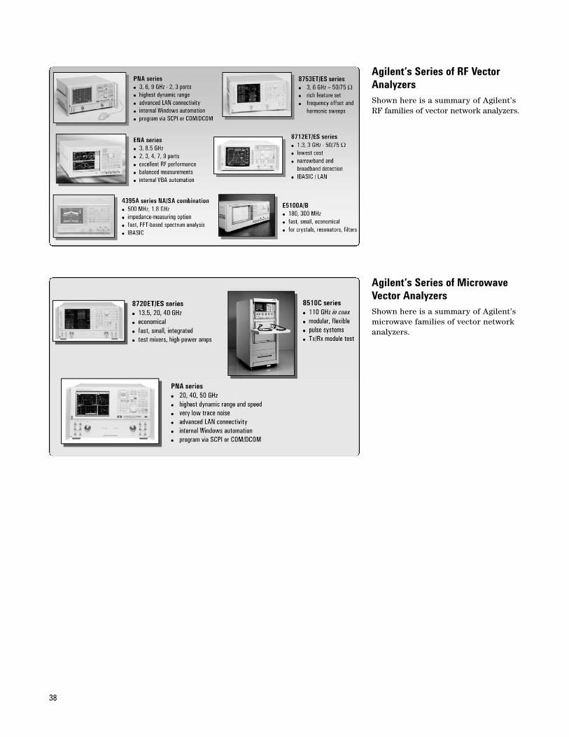
Agilent’s Series of MicrowaveVector AnalyzersShown here is a summary of Agilent’smicrowave families of vector networkanalyzers.
Agilent’s Series of RF VectorAnalyzersShown here is a summary of Agilent’sRF families of vector network analyzers.
39
AgendaIn this next section, we will talk aboutthe need for error correction and howit is accomplished. Why do we evenneed error-correction and calibration?It is impossible to make perfect hardware which obviously would notneed any form of error correction.Even making the hardware goodenough to eliminate the need for errorcorrection for most devices would beextremely expensive. The best balance is to make the hardware as good as practically possible, balancing performance and cost. Error correctionis then a very useful tool to improvemeasurement accuracy.
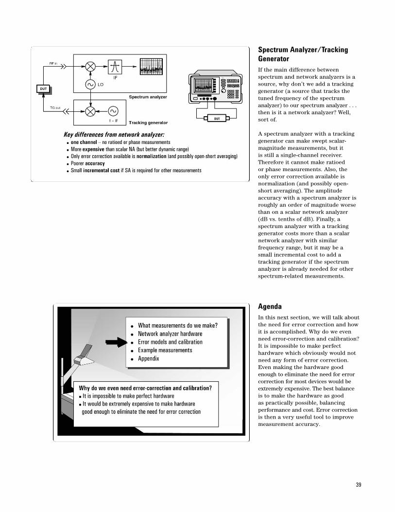
Spectrum Analyzer/TrackingGeneratorIf the main difference between spectrum and network analyzers is asource, why don’t we add a trackinggenerator (a source that tracks thetuned frequency of the spectrum analyzer) to our spectrum analyzer . . .then is it a network analyzer? Well,sort of.
A spectrum analyzer with a trackinggenerator can make swept scalar-magnitude measurements, but it is still a single-channel receiver.Therefore it cannot make ratioed or phase measurements. Also, the only error correction available is normalization (and possibly open-short averaging). The amplitude accuracy with a spectrum analyzer isroughly an order of magnitude worsethan on a scalar network analyzer (dB vs. tenths of dB). Finally, aspectrum analyzer with a trackinggenerator costs more than a scalarnetwork analyzer with similar frequency range, but it may be a small incremental cost to add a tracking generator if the spectrumanalyzer is already needed for otherspectrum-related measurements.
40
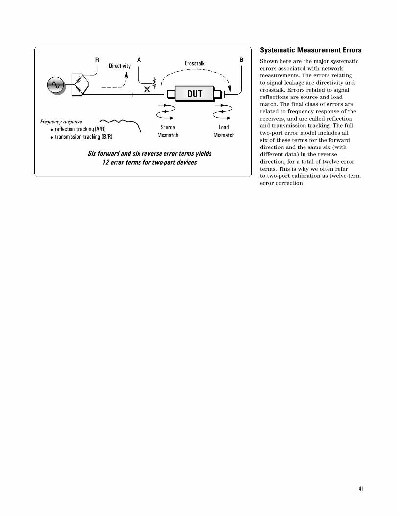
Measurement Error ModelingLet’s look at the three basic sources of measurement error: systematic,random and drift.
Systematic errors are due to imperfections in the analyzer and test setup. They are repeatable (andtherefore predictable), and areassumed to be time invariant.Systematic errors are characterizedduring the calibration process andmathematically removed during measurements.
Random errors are unpredictablesince they vary with time in a randomfashion. Therefore, they cannot beremoved by calibration. The main contributors to random error areinstrument noise (source phase noise, sampler noise, IF noise).
Drift errors are due to the instrumentor test-system performance changingafter a calibration has been done. Drift is primarily caused by temperature variation and it can be removed byfurther calibration(s). The timeframeover which a calibration remains accurate is dependent on the rate ofdrift that the test system undergoes inthe user’s test environment. Providinga stable ambient temperature usuallygoes a long way towards minimizingdrift.
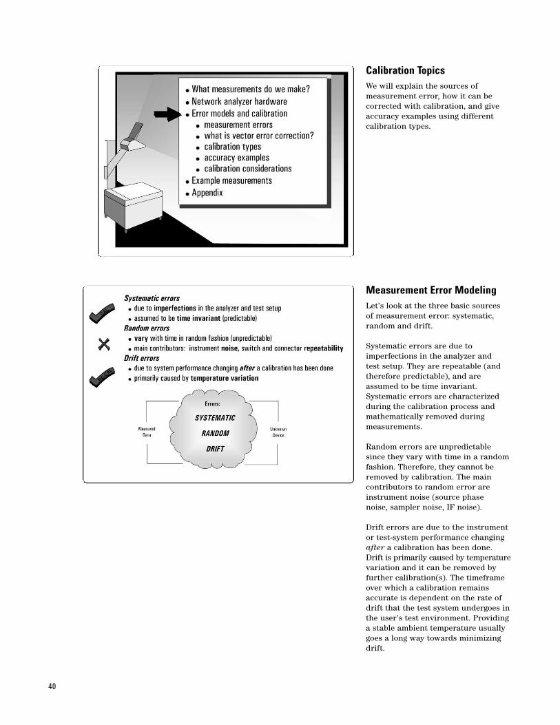
Calibration TopicsWe will explain the sources of measurement error, how it can be corrected with calibration, and giveaccuracy examples using different calibration types.
41
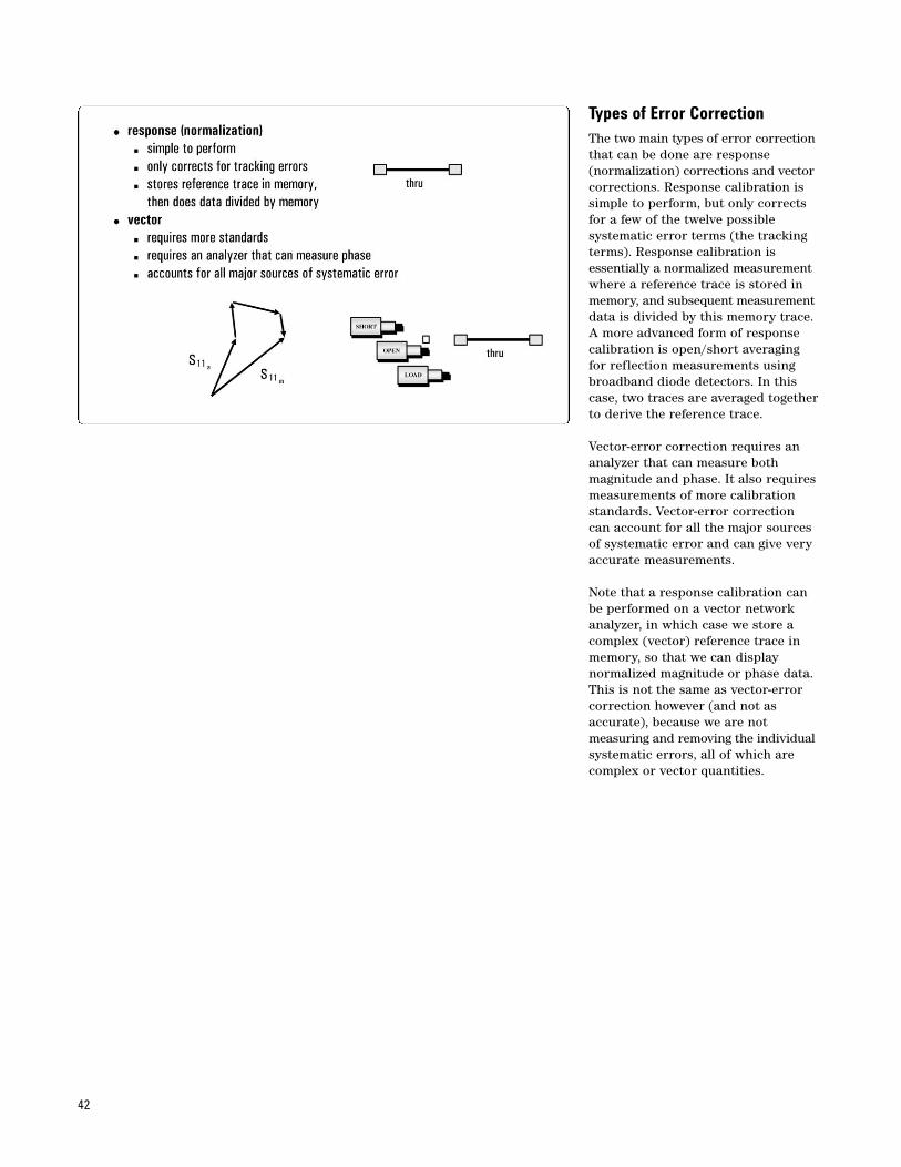
Systematic Measurement ErrorsShown here are the major systematicerrors associated with network measurements. The errors relating to signal leakage are directivity andcrosstalk. Errors related to signalreflections are source and load match. The final class of errors arerelated to frequency response of thereceivers, and are called reflectionand transmission tracking. The fulltwo-port error model includes all six of these terms for the forwarddirection and the same six (with different data) in the reverse direction, for a total of twelve errorterms. This is why we often refer to two-port calibration as twelve-termerror correction
42
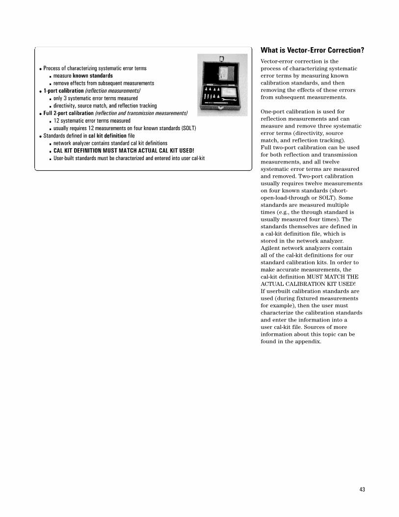
Types of Error CorrectionThe two main types of error correctionthat can be done are response (normalization) corrections and vectorcorrections. Response calibration issimple to perform, but only correctsfor a few of the twelve possible systematic error terms (the trackingterms). Response calibration is essentially a normalized measurementwhere a reference trace is stored inmemory, and subsequent measurementdata is divided by this memory trace.A more advanced form of responsecalibration is open/short averaging for reflection measurements usingbroadband diode detectors. In thiscase, two traces are averaged togetherto derive the reference trace.
Vector-error correction requires ananalyzer that can measure both magnitude and phase. It also requiresmeasurements of more calibrationstandards. Vector-error correction can account for all the major sourcesof systematic error and can give veryaccurate measurements.
Note that a response calibration canbe performed on a vector networkanalyzer, in which case we store acomplex (vector) reference trace inmemory, so that we can display normalized magnitude or phase data.This is not the same as vector-errorcorrection however (and not as accurate), because we are not measuring and removing the individualsystematic errors, all of which arecomplex or vector quantities.
43
What is Vector-Error Correction?Vector-error correction is the process of characterizing systematicerror terms by measuring known calibration standards, and thenremoving the effects of these errorsfrom subsequent measurements.
One-port calibration is used for reflection measurements and canmeasure and remove three systematicerror terms (directivity, source match, and reflection tracking). Full two-port calibration can be usedfor both reflection and transmissionmeasurements, and all twelve systematic error terms are measuredand removed. Two-port calibrationusually requires twelve measurementson four known standards (short-open-load-through or SOLT). Somestandards are measured multipletimes (e.g., the through standard isusually measured four times). Thestandards themselves are defined in a cal-kit definition file, which is stored in the network analyzer.Agilent network analyzers contain all of the cal-kit definitions for ourstandard calibration kits. In order tomake accurate measurements, the cal-kit definition MUST MATCH THEACTUAL CALIBRATION KIT USED! If userbuilt calibration standards areused (during fixtured measurementsfor example), then the user must characterize the calibration standardsand enter the information into a user cal-kit file. Sources of more information about this topic can befound in the appendix.
44
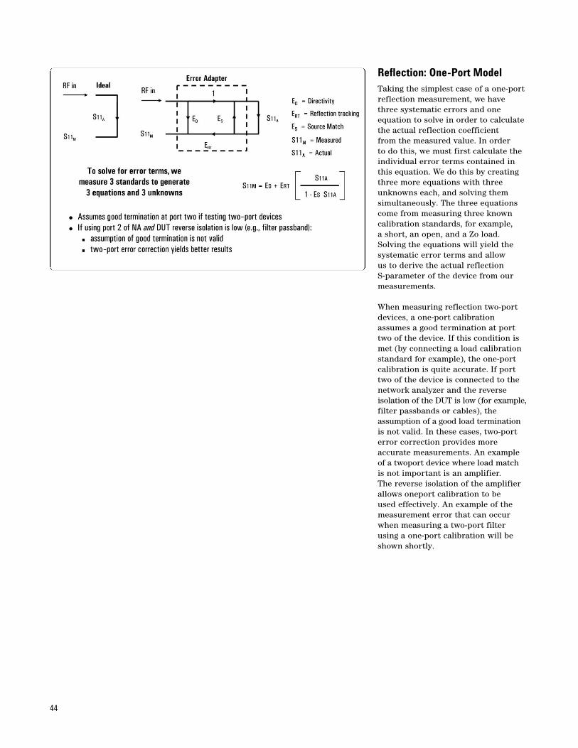
Reflection: One-Port ModelTaking the simplest case of a one-portreflection measurement, we havethree systematic errors and one equation to solve in order to calculatethe actual reflection coefficient from the measured value. In order to do this, we must first calculate theindividual error terms contained inthis equation. We do this by creatingthree more equations with threeunknowns each, and solving themsimultaneously. The three equationscome from measuring three knowncalibration standards, for example, a short, an open, and a Zo load.Solving the equations will yield thesystematic error terms and allow us to derive the actual reflection S-parameter of the device from ourmeasurements.
When measuring reflection two-portdevices, a one-port calibrationassumes a good termination at porttwo of the device. If this condition ismet (by connecting a load calibrationstandard for example), the one-portcalibration is quite accurate. If porttwo of the device is connected to thenetwork analyzer and the reverse isolation of the DUT is low (for example,filter passbands or cables), theassumption of a good load terminationis not valid. In these cases, two-porterror correction provides more accurate measurements. An exampleof a twoport device where load match is not important is an amplifier. The reverse isolation of the amplifierallows oneport calibration to be used effectively. An example of themeasurement error that can occurwhen measuring a two-port filterusing a one-port calibration will beshown shortly.
45
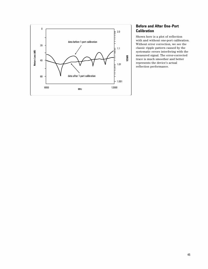
Before and After One-PortCalibrationShown here is a plot of reflection with and without one-port calibration.Without error correction, we see theclassic ripple pattern caused by thesystematic errors interfering with themeasured signal. The error-correctedtrace is much smoother and betterrepresents the device’s actual reflection performance.
46
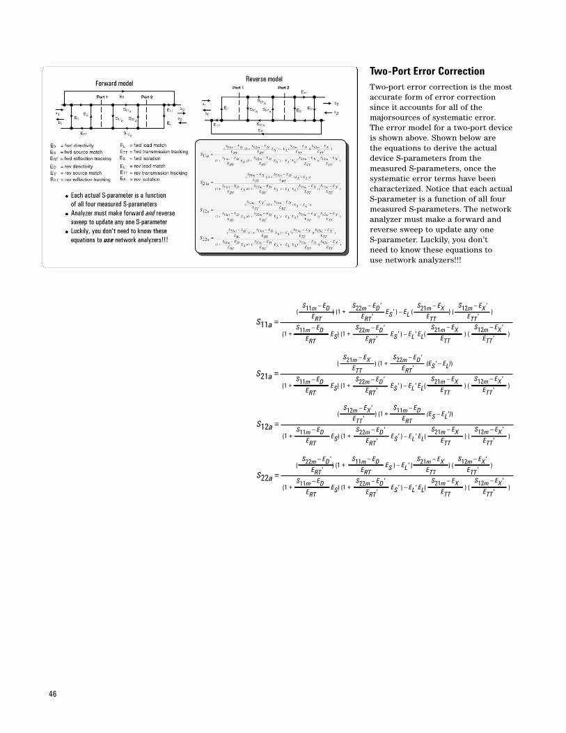
Two-Port Error CorrectionTwo-port error correction is the mostaccurate form of error correctionsince it accounts for all of the majorsources of systematic error. The error model for a two-port deviceis shown above. Shown below are the equations to derive the actualdevice S-parameters from the measured S-parameters, once the systematic error terms have beencharacterized. Notice that each actualS-parameter is a function of all fourmeasured S-parameters. The networkanalyzer must make a forward andreverse sweep to update any one S-parameter. Luckily, you don’t need to know these equations to use network analyzers!!!
S21a =
S21m – EX S22m – ED'
ETT ERT'( ) (1 + (ES' – EL))
S11m – ED S22m – ED' S12m – EX'S21m – EX(1 + ES) (1 + ES' ) – EL' EL( ) ( )
ERT ERT' ETT ETT'
S11a =S11m – ED S22m – ED' S12m – EX'S21m – EX
(1 + ES) (1 + ES' ) – EL' EL( ) ( )ERT ERT' ETT ETT'
S12a =
S12m – EX' S11m – EDETT' ERT
( ) (1 + (ES – EL'))
S11m – ED S22m – ED' S12m – EX'S21m – EX(1 + ES) (1 + ES' ) – EL' EL( ) ( )
ERT ERT' ETT ETT'
S22a =
S22m – ED' S11m – EDERT' ERT
( ) (1 + ES ) – EL'
S11m – ED S22m – ED' S12m – EX'S21m – EX(1 + ES) (1 + ES' ) – EL' EL( ) ( )
ERT ERT' ETT ETT'
S21m – EX S12m – EX'
ETT ETT'( ) ( )
S11m – ED S22m – ED'
ERT ERT'( ) (1 + ES' ) – EL
S21m – EX S12m – EX'
ETT ETT'( ) ( )
47
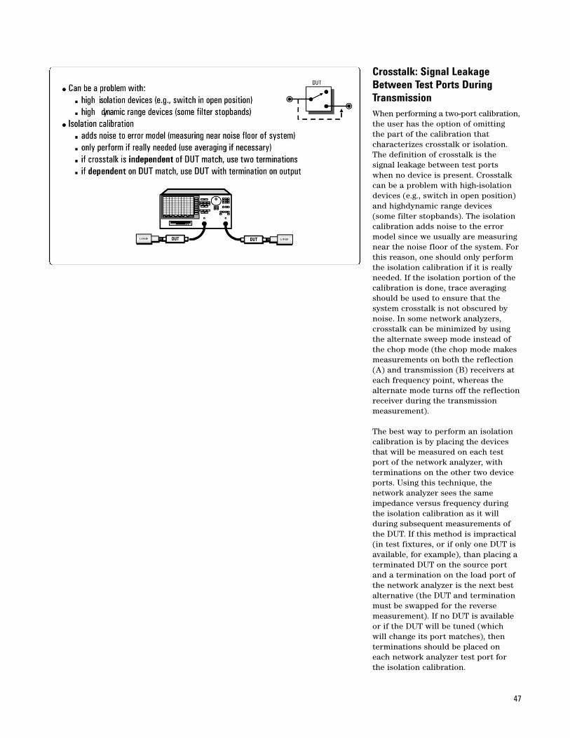
Crosstalk: Signal LeakageBetween Test Ports DuringTransmissionWhen performing a two-port calibration,the user has the option of omitting the part of the calibration that characterizes crosstalk or isolation.The definition of crosstalk is the signal leakage between test portswhen no device is present. Crosstalkcan be a problem with high-isolationdevices (e.g., switch in open position)and highdynamic range devices (some filter stopbands). The isolationcalibration adds noise to the errormodel since we usually are measuringnear the noise floor of the system. Forthis reason, one should only performthe isolation calibration if it is reallyneeded. If the isolation portion of thecalibration is done, trace averagingshould be used to ensure that the system crosstalk is not obscured bynoise. In some network analyzers,crosstalk can be minimized by usingthe alternate sweep mode instead ofthe chop mode (the chop mode makesmeasurements on both the reflection(A) and transmission (B) receivers ateach frequency point, whereas thealternate mode turns off the reflectionreceiver during the transmissionmeasurement).
The best way to perform an isolationcalibration is by placing the devicesthat will be measured on each testport of the network analyzer, with terminations on the other two deviceports. Using this technique, the network analyzer sees the sameimpedance versus frequency duringthe isolation calibration as it will during subsequent measurements ofthe DUT. If this method is impractical(in test fixtures, or if only one DUT isavailable, for example), than placing aterminated DUT on the source portand a termination on the load port ofthe network analyzer is the next bestalternative (the DUT and terminationmust be swapped for the reversemeasurement). If no DUT is availableor if the DUT will be tuned (which will change its port matches), thenterminations should be placed on each network analyzer test port forthe isolation calibration.
48
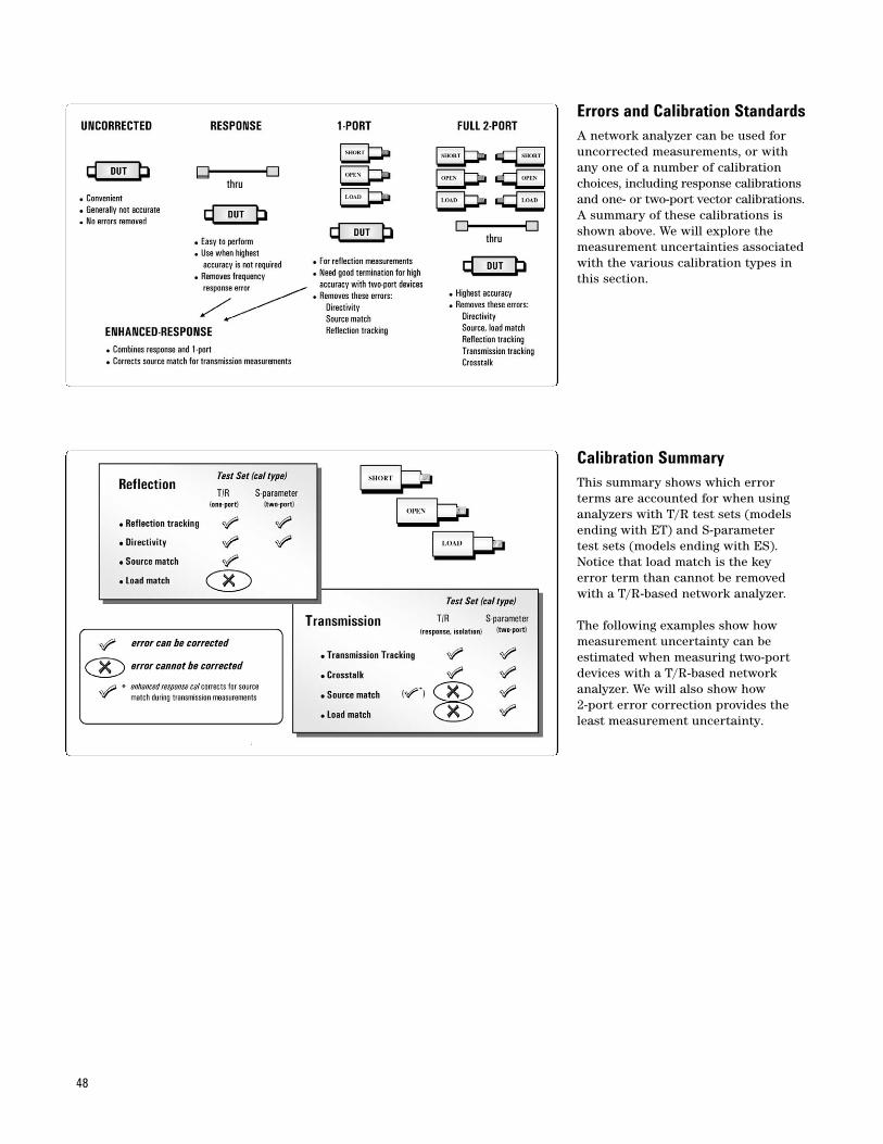
Errors and Calibration StandardsA network analyzer can be used foruncorrected measurements, or withany one of a number of calibrationchoices, including response calibrationsand one- or two-port vector calibrations.A summary of these calibrations isshown above. We will explore themeasurement uncertainties associatedwith the various calibration types inthis section.
Calibration SummaryThis summary shows which errorterms are accounted for when usinganalyzers with T/R test sets (modelsending with ET) and S-parameter test sets (models ending with ES).Notice that load match is the key error term than cannot be removedwith a T/R-based network analyzer.
The following examples show howmeasurement uncertainty can be estimated when measuring two-portdevices with a T/R-based network analyzer. We will also show how 2-port error correction provides theleast measurement uncertainty.
49
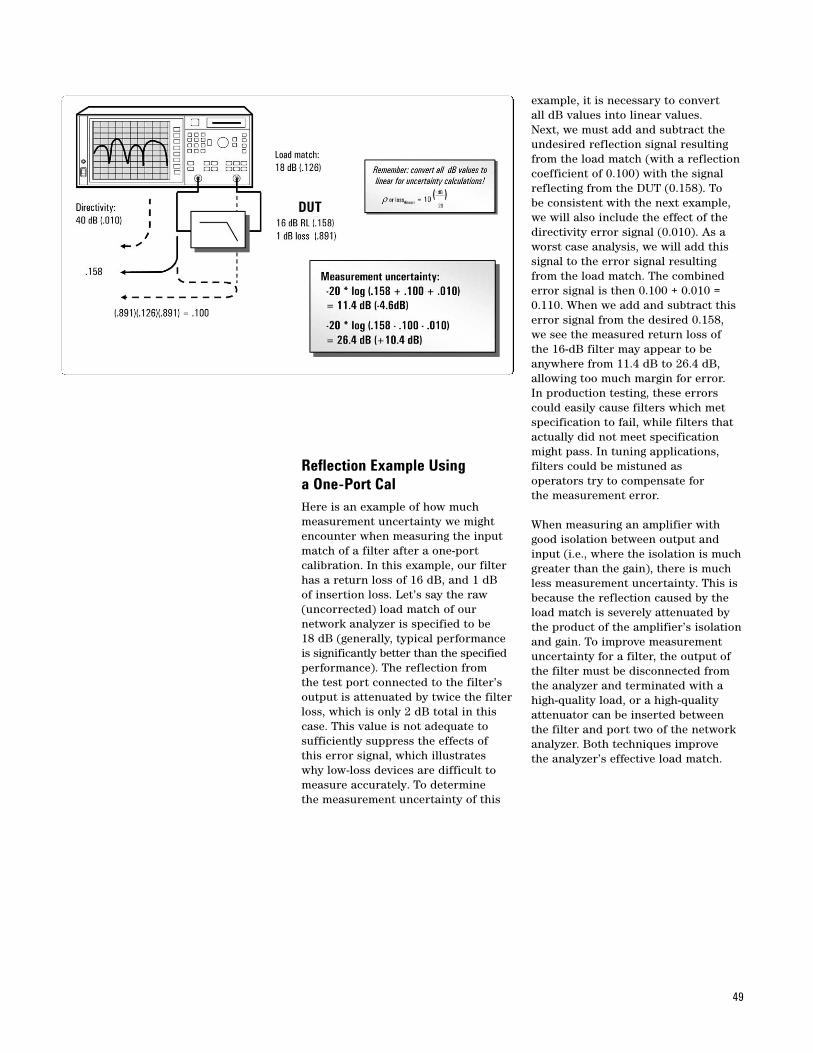
Reflection Example Using a One-Port CalHere is an example of how muchmeasurement uncertainty we mightencounter when measuring the inputmatch of a filter after a one-port calibration. In this example, our filterhas a return loss of 16 dB, and 1 dB of insertion loss. Let’s say the raw(uncorrected) load match of our network analyzer is specified to be 18 dB (generally, typical performanceis significantly better than the specifiedperformance). The reflection from the test port connected to the filter’soutput is attenuated by twice the filterloss, which is only 2 dB total in thiscase. This value is not adequate to sufficiently suppress the effects of this error signal, which illustrates why low-loss devices are difficult tomeasure accurately. To determine the measurement uncertainty of this
example, it is necessary to convert all dB values into linear values. Next, we must add and subtract theundesired reflection signal resultingfrom the load match (with a reflectioncoefficient of 0.100) with the signalreflecting from the DUT (0.158). To be consistent with the next example,we will also include the effect of thedirectivity error signal (0.010). As aworst case analysis, we will add thissignal to the error signal resultingfrom the load match. The combinederror signal is then 0.100 + 0.010 =0.110. When we add and subtract thiserror signal from the desired 0.158, we see the measured return loss of the 16-dB filter may appear to be anywhere from 11.4 dB to 26.4 dB,allowing too much margin for error. In production testing, these errorscould easily cause filters which metspecification to fail, while filters thatactually did not meet specificationmight pass. In tuning applications, filters could be mistuned as operators try to compensate for the measurement error.
When measuring an amplifier withgood isolation between output andinput (i.e., where the isolation is muchgreater than the gain), there is muchless measurement uncertainty. This isbecause the reflection caused by theload match is severely attenuated bythe product of the amplifier’s isolationand gain. To improve measurementuncertainty for a filter, the output ofthe filter must be disconnected fromthe analyzer and terminated with ahigh-quality load, or a high-qualityattenuator can be inserted betweenthe filter and port two of the networkanalyzer. Both techniques improve the analyzer’s effective load match.
50
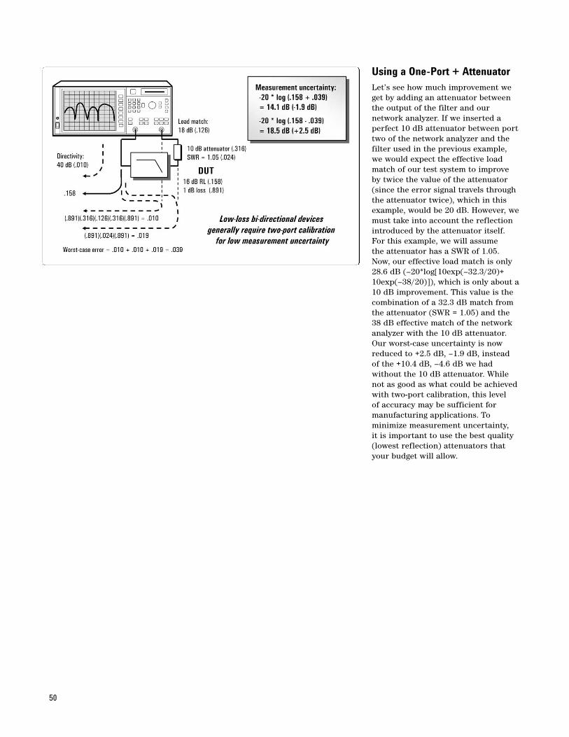
Using a One-Port + AttenuatorLet’s see how much improvement weget by adding an attenuator betweenthe output of the filter and our network analyzer. If we inserted a perfect 10 dB attenuator between porttwo of the network analyzer and thefilter used in the previous example,we would expect the effective loadmatch of our test system to improveby twice the value of the attenuator(since the error signal travels throughthe attenuator twice), which in thisexample, would be 20 dB. However, wemust take into account the reflectionintroduced by the attenuator itself.For this example, we will assume the attenuator has a SWR of 1.05.Now, our effective load match is only28.6 dB (–20*log[10exp(–32.3/20)+10exp(–38/20)]), which is only about a10 dB improvement. This value is thecombination of a 32.3 dB match fromthe attenuator (SWR = 1.05) and the38 dB effective match of the networkanalyzer with the 10 dB attenuator.Our worst-case uncertainty is nowreduced to +2.5 dB, –1.9 dB, instead of the +10.4 dB, –4.6 dB we had without the 10 dB attenuator. Whilenot as good as what could be achievedwith two-port calibration, this level of accuracy may be sufficient for manufacturing applications. To minimize measurement uncertainty, it is important to use the best quality(lowest reflection) attenuators thatyour budget will allow.
51
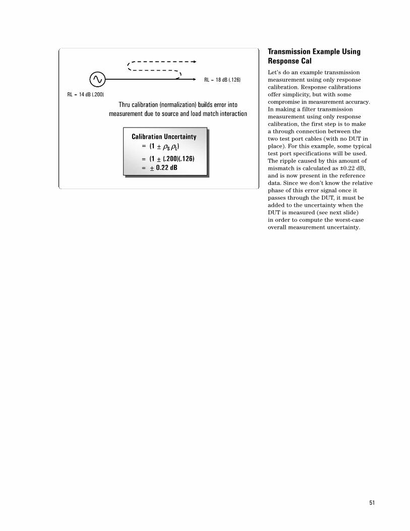
Transmission Example UsingResponse CalLet’s do an example transmissionmeasurement using only response calibration. Response calibrationsoffer simplicity, but with some compromise in measurement accuracy.In making a filter transmission measurement using only response calibration, the first step is to make a through connection between the two test port cables (with no DUT inplace). For this example, some typicaltest port specifications will be used.The ripple caused by this amount ofmismatch is calculated as ±0.22 dB,and is now present in the referencedata. Since we don’t know the relativephase of this error signal once it passes through the DUT, it must beadded to the uncertainty when theDUT is measured (see next slide) in order to compute the worst-caseoverall measurement uncertainty.
52
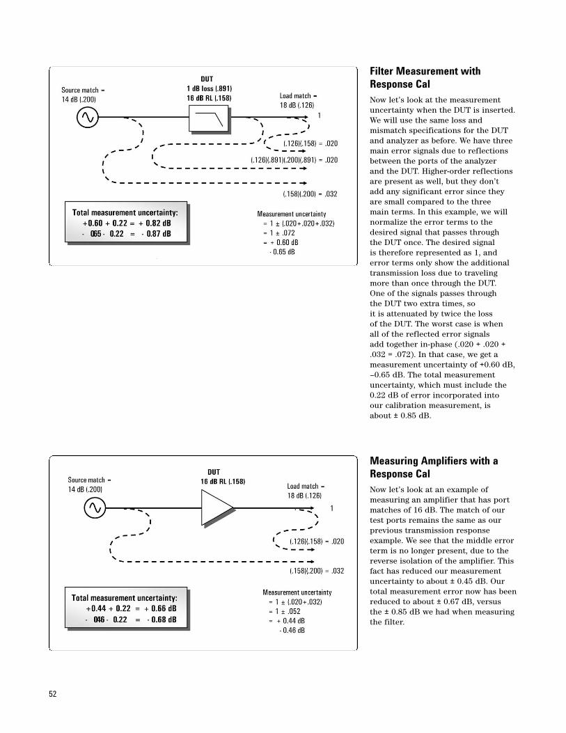
Measuring Amplifiers with aResponse CalNow let’s look at an example of measuring an amplifier that has portmatches of 16 dB. The match of ourtest ports remains the same as ourprevious transmission response example. We see that the middle errorterm is no longer present, due to thereverse isolation of the amplifier. Thisfact has reduced our measurementuncertainty to about ± 0.45 dB. Ourtotal measurement error now has beenreduced to about ± 0.67 dB, versus the ± 0.85 dB we had when measuringthe filter.
Filter Measurement withResponse CalNow let’s look at the measurementuncertainty when the DUT is inserted.We will use the same loss and mismatch specifications for the DUTand analyzer as before. We have threemain error signals due to reflectionsbetween the ports of the analyzer and the DUT. Higher-order reflectionsare present as well, but they don’t add any significant error since theyare small compared to the three main terms. In this example, we willnormalize the error terms to thedesired signal that passes through the DUT once. The desired signal is therefore represented as 1, anderror terms only show the additionaltransmission loss due to travelingmore than once through the DUT. One of the signals passes through the DUT two extra times, so it is attenuated by twice the loss of the DUT. The worst case is when all of the reflected error signals add together in-phase (.020 + .020 +.032 = .072). In that case, we get ameasurement uncertainty of +0.60 dB,–0.65 dB. The total measurementuncertainty, which must include the0.22 dB of error incorporated into our calibration measurement, is about ± 0.85 dB.
53
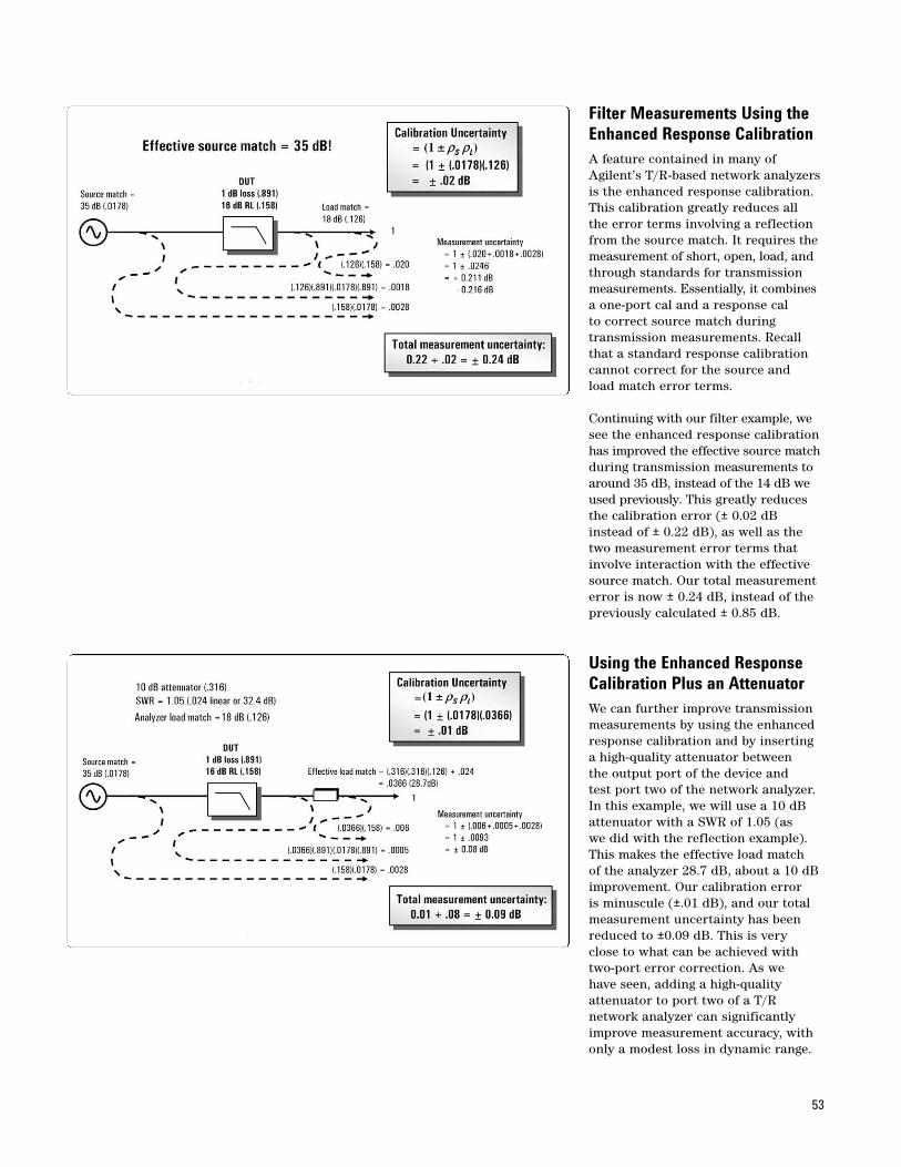
Using the Enhanced ResponseCalibration Plus an AttenuatorWe can further improve transmissionmeasurements by using the enhancedresponse calibration and by insertinga high-quality attenuator between the output port of the device and test port two of the network analyzer.In this example, we will use a 10 dBattenuator with a SWR of 1.05 (as we did with the reflection example).This makes the effective load match of the analyzer 28.7 dB, about a 10 dBimprovement. Our calibration error is minuscule (±.01 dB), and our totalmeasurement uncertainty has beenreduced to ±0.09 dB. This is very close to what can be achieved withtwo-port error correction. As we have seen, adding a high-quality attenuator to port two of a T/R network analyzer can significantlyimprove measurement accuracy, withonly a modest loss in dynamic range.
Filter Measurements Using theEnhanced Response CalibrationA feature contained in many ofAgilent’s T/R-based network analyzersis the enhanced response calibration.This calibration greatly reduces all the error terms involving a reflectionfrom the source match. It requires themeasurement of short, open, load, andthrough standards for transmissionmeasurements. Essentially, it combinesa one-port cal and a response cal to correct source match during transmission measurements. Recallthat a standard response calibrationcannot correct for the source and load match error terms.
Continuing with our filter example, wesee the enhanced response calibrationhas improved the effective source matchduring transmission measurements toaround 35 dB, instead of the 14 dB weused previously. This greatly reducesthe calibration error (± 0.02 dBinstead of ± 0.22 dB), as well as thetwo measurement error terms thatinvolve interaction with the effectivesource match. Our total measurementerror is now ± 0.24 dB, instead of thepreviously calculated ± 0.85 dB.
54
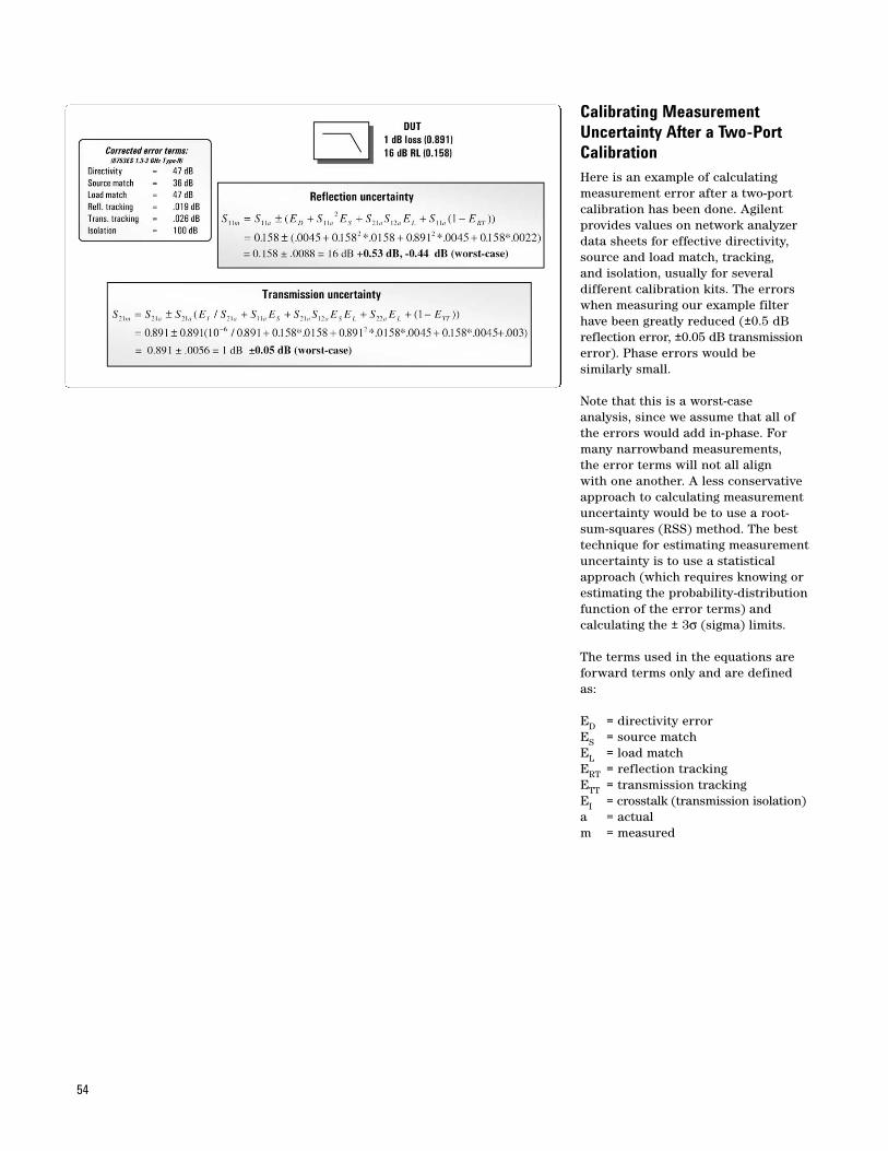
Calibrating MeasurementUncertainty After a Two-PortCalibrationHere is an example of calculatingmeasurement error after a two-portcalibration has been done. Agilentprovides values on network analyzerdata sheets for effective directivity,source and load match, tracking, and isolation, usually for several different calibration kits. The errorswhen measuring our example filterhave been greatly reduced (±0.5 dBreflection error, ±0.05 dB transmissionerror). Phase errors would be similarly small.
Note that this is a worst-case analysis, since we assume that all ofthe errors would add in-phase. Formany narrowband measurements, the error terms will not all align with one another. A less conservativeapproach to calculating measurementuncertainty would be to use a root-sum-squares (RSS) method. The besttechnique for estimating measurementuncertainty is to use a statisticalapproach (which requires knowing orestimating the probability-distributionfunction of the error terms) and calculating the ± 3σ (sigma) limits.
The terms used in the equations areforward terms only and are definedas:
ED = directivity errorES = source matchEL = load matchERT = reflection trackingETT = transmission trackingEI = crosstalk (transmission isolation)a = actualm = measured
55
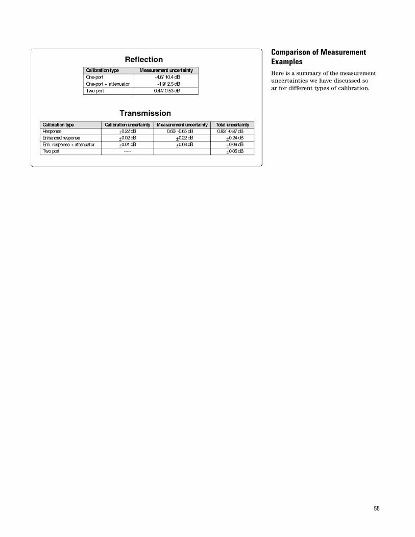
Comparison of MeasurementExamplesHere is a summary of the measurementuncertainties we have discussed so ar for different types of calibration.
56
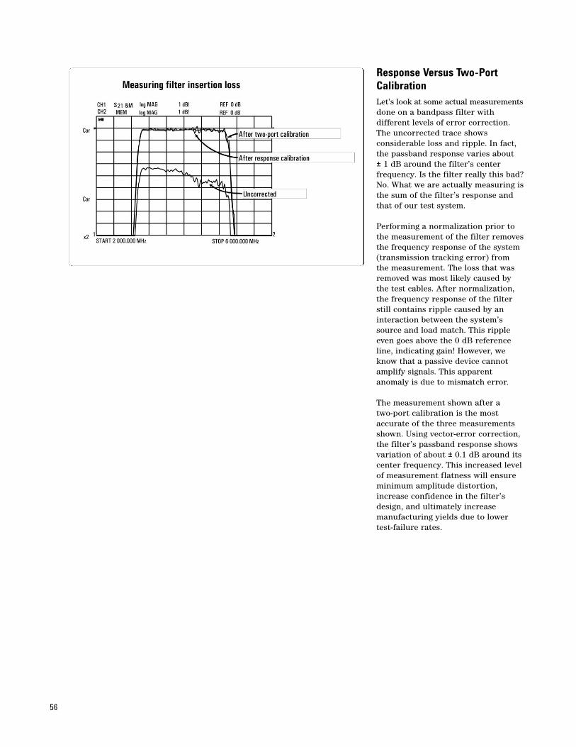
Response Versus Two-PortCalibrationLet’s look at some actual measurementsdone on a bandpass filter with different levels of error correction.The uncorrected trace shows considerable loss and ripple. In fact,the passband response varies about ± 1 dB around the filter’s center frequency. Is the filter really this bad?No. What we are actually measuring isthe sum of the filter’s response andthat of our test system.
Performing a normalization prior tothe measurement of the filter removesthe frequency response of the system(transmission tracking error) from the measurement. The loss that wasremoved was most likely caused by the test cables. After normalization,the frequency response of the filterstill contains ripple caused by aninteraction between the system’ssource and load match. This rippleeven goes above the 0 dB referenceline, indicating gain! However, weknow that a passive device cannotamplify signals. This apparent anomaly is due to mismatch error.
The measurement shown after a two-port calibration is the most accurate of the three measurementsshown. Using vector-error correction,the filter’s passband response showsvariation of about ± 0.1 dB around itscenter frequency. This increased levelof measurement flatness will ensureminimum amplitude distortion,increase confidence in the filter’sdesign, and ultimately increase manufacturing yields due to lowertest-failure rates.
57
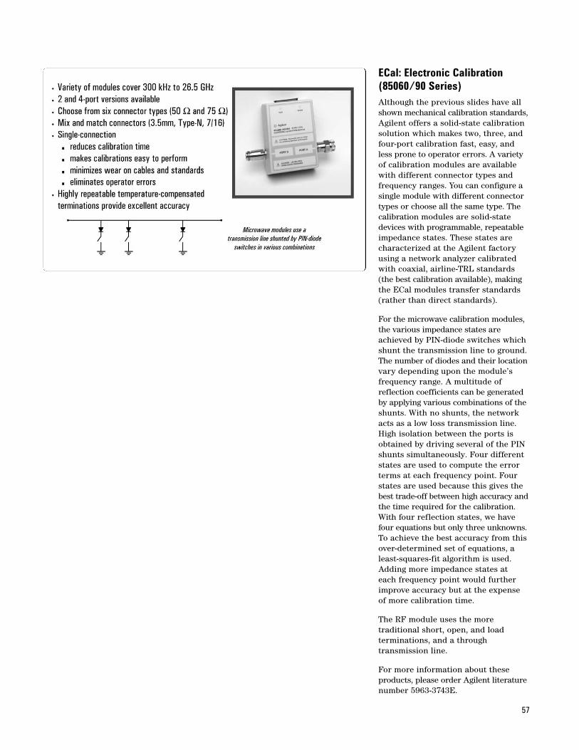
ECal: Electronic Calibration(85060/90 Series)Although the previous slides have allshown mechanical calibration standards,Agilent offers a solid-state calibrationsolution which makes two, three, andfour-port calibration fast, easy, andless prone to operator errors. A varietyof calibration modules are availablewith different connector types andfrequency ranges. You can configure asingle module with different connectortypes or choose all the same type. Thecalibration modules are solid-statedevices with programmable, repeatableimpedance states. These states arecharacterized at the Agilent factoryusing a network analyzer calibratedwith coaxial, airline-TRL standards(the best calibration available), makingthe ECal modules transfer standards(rather than direct standards).
For the microwave calibration modules,the various impedance states areachieved by PIN-diode switches whichshunt the transmission line to ground.The number of diodes and their locationvary depending upon the module’s frequency range. A multitude of reflection coefficients can be generatedby applying various combinations of theshunts. With no shunts, the networkacts as a low loss transmission line.High isolation between the ports isobtained by driving several of the PINshunts simultaneously. Four differentstates are used to compute the errorterms at each frequency point. Fourstates are used because this gives thebest trade-off between high accuracy andthe time required for the calibration.With four reflection states, we havefour equations but only three unknowns.To achieve the best accuracy from thisover-determined set of equations, aleast-squares-fit algorithm is used.Adding more impedance states at each frequency point would furtherimprove accuracy but at the expenseof more calibration time.
The RF module uses the more traditional short, open, and load terminations, and a through transmission line.
For more information about theseproducts, please order Agilent literaturenumber 5963-3743E.
58
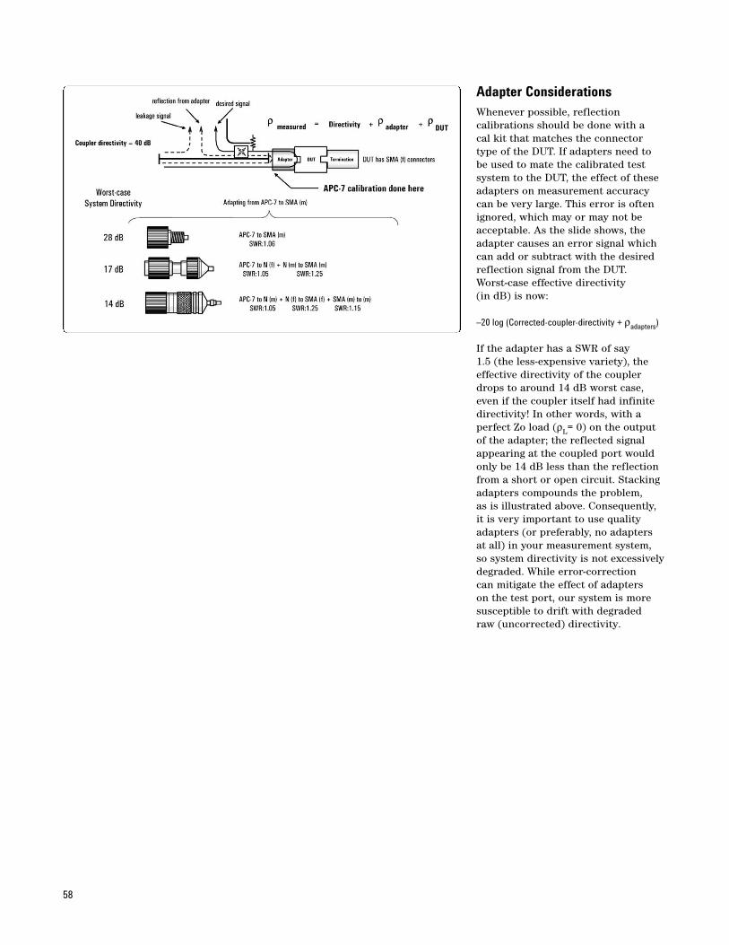
Adapter ConsiderationsWhenever possible, reflection calibrations should be done with a cal kit that matches the connectortype of the DUT. If adapters need to be used to mate the calibrated testsystem to the DUT, the effect of theseadapters on measurement accuracycan be very large. This error is oftenignored, which may or may not beacceptable. As the slide shows, theadapter causes an error signal whichcan add or subtract with the desiredreflection signal from the DUT. Worst-case effective directivity (in dB) is now:
–20 log (Corrected-coupler-directivity + ρadapters)
If the adapter has a SWR of say 1.5 (the less-expensive variety), theeffective directivity of the couplerdrops to around 14 dB worst case,even if the coupler itself had infinitedirectivity! In other words, with a perfect Zo load (ρL= 0) on the outputof the adapter; the reflected signalappearing at the coupled port wouldonly be 14 dB less than the reflectionfrom a short or open circuit. Stackingadapters compounds the problem, as is illustrated above. Consequently,it is very important to use qualityadapters (or preferably, no adapters at all) in your measurement system, so system directivity is not excessivelydegraded. While error-correction can mitigate the effect of adapters on the test port, our system is moresusceptible to drift with degraded raw (uncorrected) directivity.
59
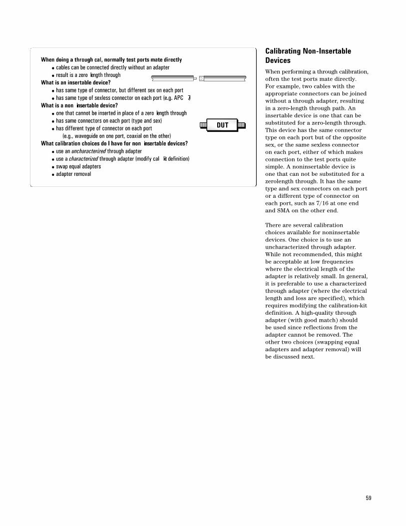
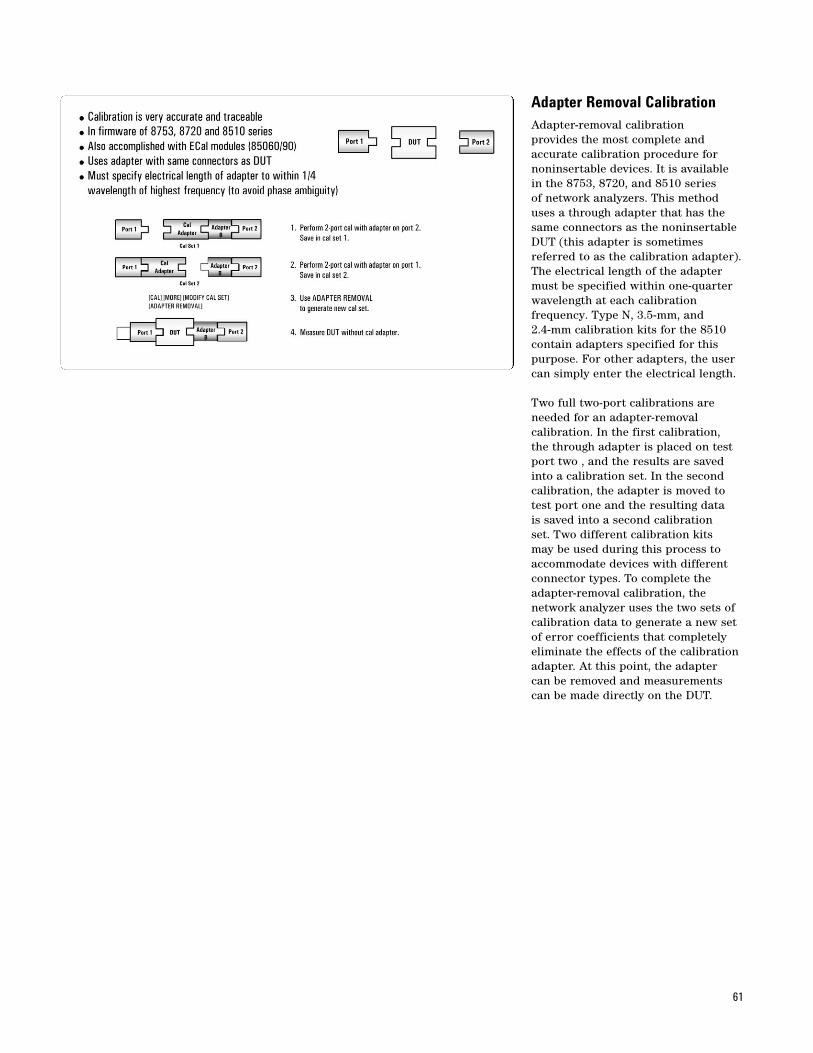
Calibrating Non-InsertableDevicesWhen performing a through calibration,often the test ports mate directly. For example, two cables with theappropriate connectors can be joinedwithout a through adapter, resultingin a zero-length through path. Aninsertable device is one that can besubstituted for a zero-length through.This device has the same connectortype on each port but of the oppositesex, or the same sexless connector on each port, either of which makesconnection to the test ports quite simple. A noninsertable device is one that can not be substituted for azerolength through. It has the sametype and sex connectors on each portor a different type of connector oneach port, such as 7/16 at one end and SMA on the other end.
There are several calibration choices available for noninsertabledevices. One choice is to use anuncharacterized through adapter.While not recommended, this might be acceptable at low frequencieswhere the electrical length of theadapter is relatively small. In general,it is preferable to use a characterizedthrough adapter (where the electricallength and loss are specified), whichrequires modifying the calibration-kitdefinition. A high-quality throughadapter (with good match) should be used since reflections from theadapter cannot be removed. The other two choices (swapping equaladapters and adapter removal) will be discussed next.
60
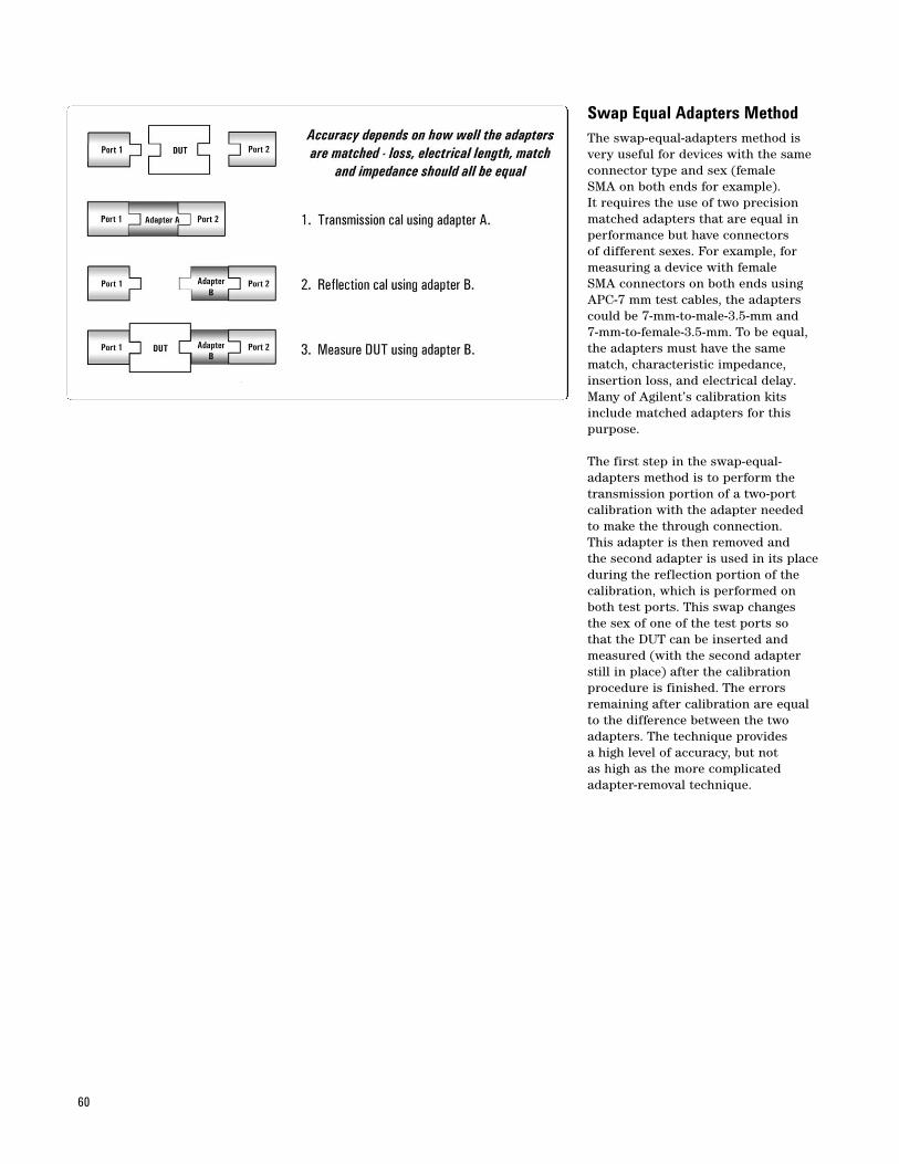
Swap Equal Adapters MethodThe swap-equal-adapters method isvery useful for devices with the sameconnector type and sex (female SMA on both ends for example). It requires the use of two precisionmatched adapters that are equal inperformance but have connectors of different sexes. For example, formeasuring a device with female SMA connectors on both ends usingAPC-7 mm test cables, the adapterscould be 7-mm-to-male-3.5-mm and 7-mm-to-female-3.5-mm. To be equal,the adapters must have the samematch, characteristic impedance,insertion loss, and electrical delay.Many of Agilent’s calibration kitsinclude matched adapters for this purpose.
The first step in the swap-equal-adapters method is to perform thetransmission portion of a two-port calibration with the adapter needed to make the through connection. This adapter is then removed and the second adapter is used in its placeduring the reflection portion of thecalibration, which is performed onboth test ports. This swap changes the sex of one of the test ports so that the DUT can be inserted andmeasured (with the second adapterstill in place) after the calibration procedure is finished. The errorsremaining after calibration are equalto the difference between the twoadapters. The technique provides a high level of accuracy, but not as high as the more complicatedadapter-removal technique.
61
Adapter Removal CalibrationAdapter-removal calibration provides the most complete and accurate calibration procedure fornoninsertable devices. It is availablein the 8753, 8720, and 8510 series of network analyzers. This methoduses a through adapter that has thesame connectors as the noninsertableDUT (this adapter is sometimesreferred to as the calibration adapter).The electrical length of the adaptermust be specified within one-quarterwavelength at each calibration frequency. Type N, 3.5-mm, and 2.4-mm calibration kits for the 8510contain adapters specified for thispurpose. For other adapters, the usercan simply enter the electrical length.
Two full two-port calibrations areneeded for an adapter-removal calibration. In the first calibration, the through adapter is placed on testport two , and the results are savedinto a calibration set. In the secondcalibration, the adapter is moved totest port one and the resulting data is saved into a second calibration set. Two different calibration kits may be used during this process toaccommodate devices with differentconnector types. To complete theadapter-removal calibration, the network analyzer uses the two sets ofcalibration data to generate a new setof error coefficients that completelyeliminate the effects of the calibrationadapter. At this point, the adapter can be removed and measurementscan be made directly on the DUT.
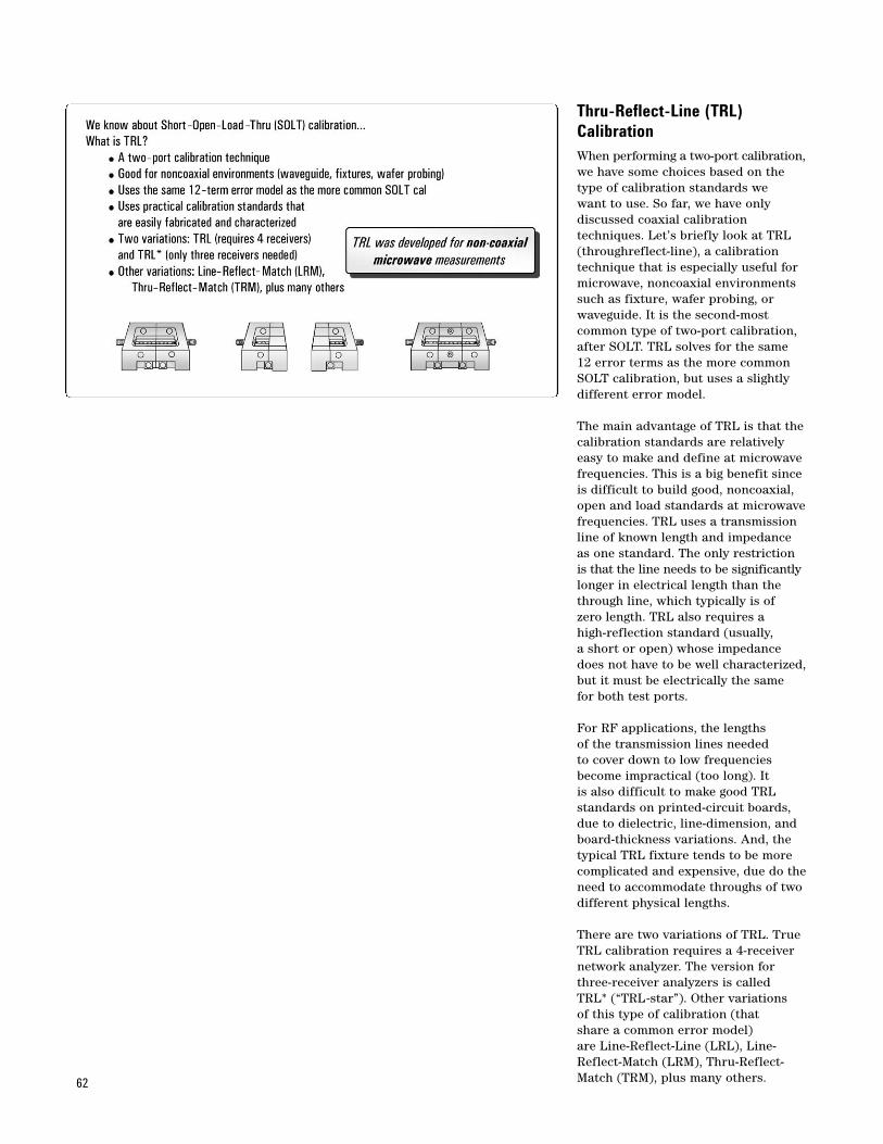
62
Thru-Reflect-Line (TRL)CalibrationWhen performing a two-port calibration,we have some choices based on thetype of calibration standards we want to use. So far, we have only discussed coaxial calibration techniques. Let’s briefly look at TRL(throughreflect-line), a calibrationtechnique that is especially useful formicrowave, noncoaxial environmentssuch as fixture, wafer probing, orwaveguide. It is the second-most common type of two-port calibration,after SOLT. TRL solves for the same 12 error terms as the more commonSOLT calibration, but uses a slightlydifferent error model.
The main advantage of TRL is that thecalibration standards are relativelyeasy to make and define at microwavefrequencies. This is a big benefit sinceis difficult to build good, noncoaxial,open and load standards at microwavefrequencies. TRL uses a transmissionline of known length and impedanceas one standard. The only restrictionis that the line needs to be significantlylonger in electrical length than thethrough line, which typically is of zero length. TRL also requires a high-reflection standard (usually, a short or open) whose impedancedoes not have to be well characterized,but it must be electrically the same for both test ports.
For RF applications, the lengths of the transmission lines needed to cover down to low frequenciesbecome impractical (too long). It is also difficult to make good TRLstandards on printed-circuit boards,due to dielectric, line-dimension, andboard-thickness variations. And, thetypical TRL fixture tends to be morecomplicated and expensive, due do theneed to accommodate throughs of twodifferent physical lengths.
There are two variations of TRL. TrueTRL calibration requires a 4-receivernetwork analyzer. The version forthree-receiver analyzers is called TRL* (“TRL-star”). Other variations of this type of calibration (that share a common error model) are Line-Reflect-Line (LRL), Line-Reflect-Match (LRM), Thru-Reflect-Match (TRM), plus many others.
63
AgendaThis section will cover some typicalmeasurements. We will look at swept-frequency testing of filters andswept-power testing of amplifiers.
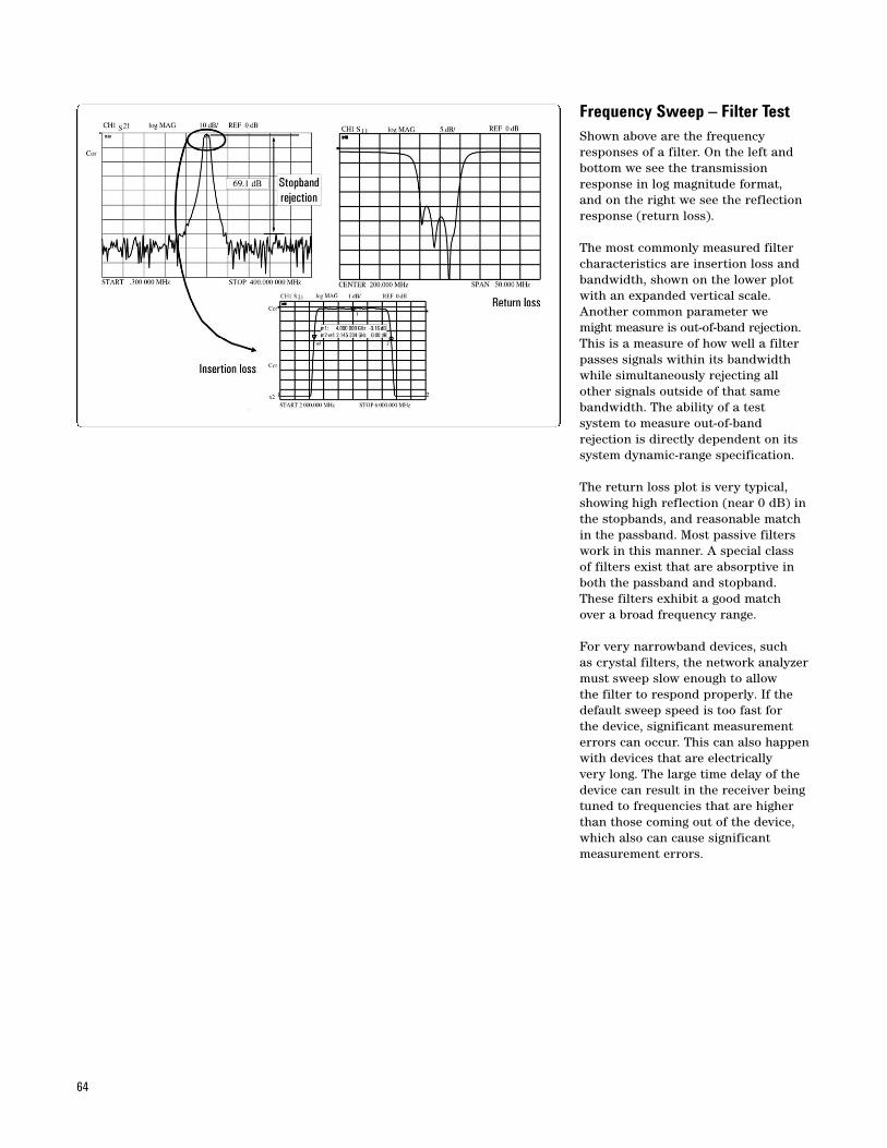
64
Frequency Sweep – Filter TestShown above are the frequencyresponses of a filter. On the left andbottom we see the transmissionresponse in log magnitude format, and on the right we see the reflectionresponse (return loss).
The most commonly measured filtercharacteristics are insertion loss andbandwidth, shown on the lower plotwith an expanded vertical scale.Another common parameter we might measure is out-of-band rejection.This is a measure of how well a filterpasses signals within its bandwidthwhile simultaneously rejecting allother signals outside of that samebandwidth. The ability of a test system to measure out-of-band rejection is directly dependent on itssystem dynamic-range specification.
The return loss plot is very typical,showing high reflection (near 0 dB) inthe stopbands, and reasonable matchin the passband. Most passive filterswork in this manner. A special class of filters exist that are absorptive inboth the passband and stopband.These filters exhibit a good matchover a broad frequency range.
For very narrowband devices, such as crystal filters, the network analyzermust sweep slow enough to allow the filter to respond properly. If thedefault sweep speed is too fast for the device, significant measurementerrors can occur. This can also happenwith devices that are electrically very long. The large time delay of thedevice can result in the receiver beingtuned to frequencies that are higherthan those coming out of the device,which also can cause significant measurement errors.
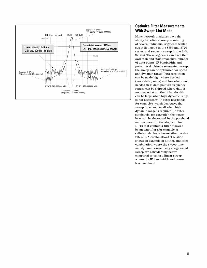
65
Optimize Filter MeasurementsWith Swept-List ModeMany network analyzers have the ability to define a sweep consisting of several individual segments (calledswept-list mode in the 8753 and 8720series, and segment sweep in the PNASeries). These segments can have theirown stop and start frequency, numberof data points, IF bandwidth, andpower level. Using a segmented sweep,the sweep can be optimized for speedand dynamic range. Data resolutioncan be made high where needed (more data points) and low where notneeded (less data points); frequencyranges can be skipped where data isnot needed at all; the IF bandwidthcan be large when high dynamic rangeis not necessary (in filter passbands,for example), which decreases thesweep time, and small when highdynamic range is required (in filterstopbands, for example); the powerlevel can be decreased in the passbandand increased in the stopband forDUTs that contain a filter followed by an amplifier (for example, a cellular-telephone base-station receivefilter/LNA combination). The slideshows an example of a filter/amplifiercombination where the sweep timeand dynamic range using a segmentedsweep are considerably better compared to using a linear sweep,where the IF bandwidth and powerlevel are fixed.
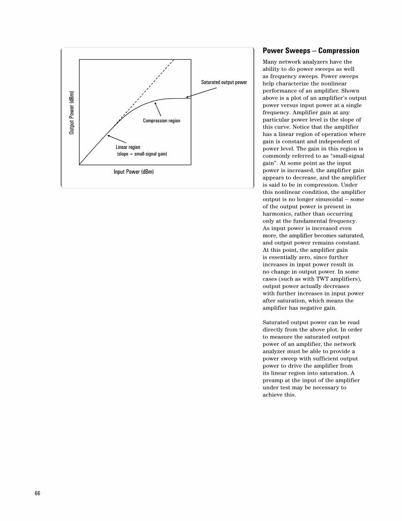
66
Power Sweeps – CompressionMany network analyzers have the ability to do power sweeps as well as frequency sweeps. Power sweepshelp characterize the nonlinear performance of an amplifier. Shownabove is a plot of an amplifier’s outputpower versus input power at a singlefrequency. Amplifier gain at any particular power level is the slope ofthis curve. Notice that the amplifierhas a linear region of operation wheregain is constant and independent ofpower level. The gain in this region iscommonly referred to as “small-signalgain”. At some point as the inputpower is increased, the amplifier gainappears to decrease, and the amplifieris said to be in compression. Underthis nonlinear condition, the amplifieroutput is no longer sinusoidal — someof the output power is present in harmonics, rather than occurring only at the fundamental frequency. As input power is increased evenmore, the amplifier becomes saturated,and output power remains constant.At this point, the amplifier gain is essentially zero, since furtherincreases in input power result in no change in output power. In somecases (such as with TWT amplifiers),output power actually decreases with further increases in input powerafter saturation, which means theamplifier has negative gain.
Saturated output power can be readdirectly from the above plot. In orderto measure the saturated outputpower of an amplifier, the networkanalyzer must be able to provide apower sweep with sufficient outputpower to drive the amplifier from its linear region into saturation. Apreamp at the input of the amplifierunder test may be necessary toachieve this.
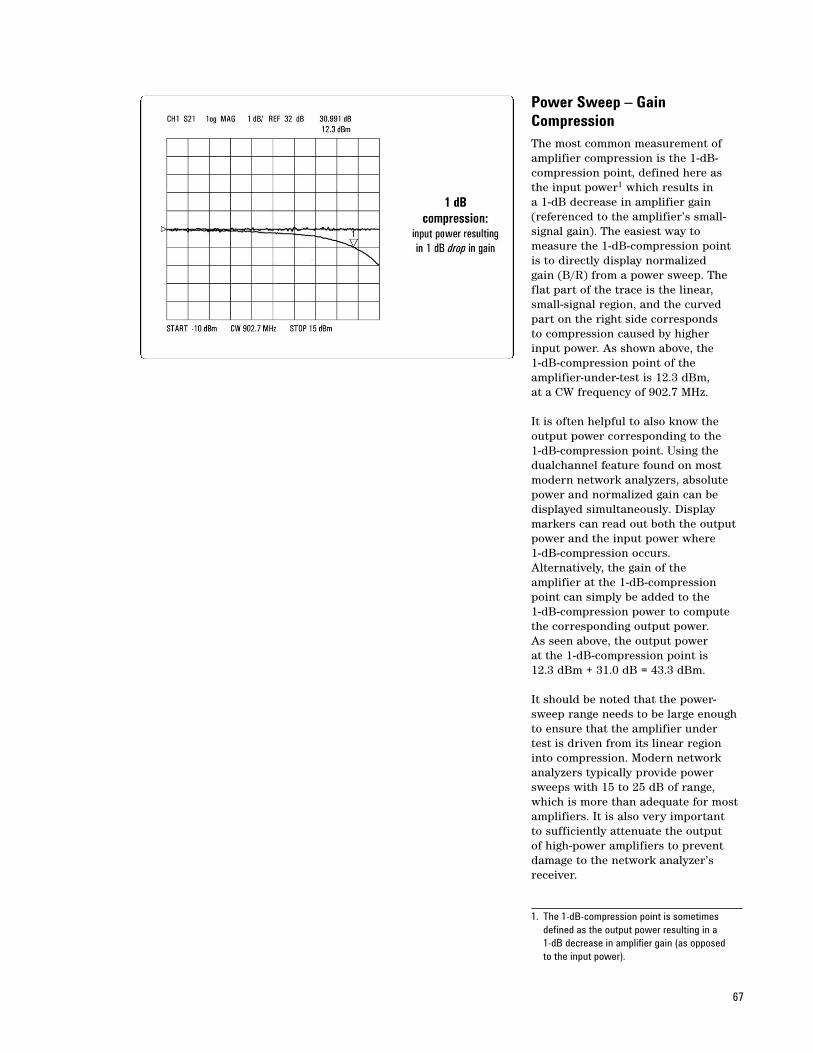
67
Power Sweep – GainCompressionThe most common measurement ofamplifier compression is the 1-dB-compression point, defined here asthe input power1 which results in a 1-dB decrease in amplifier gain (referenced to the amplifier’s small-signal gain). The easiest way to measure the 1-dB-compression pointis to directly display normalized gain (B/R) from a power sweep. Theflat part of the trace is the linear,small-signal region, and the curvedpart on the right side corresponds to compression caused by higher input power. As shown above, the 1-dB-compression point of the amplifier-under-test is 12.3 dBm, at a CW frequency of 902.7 MHz.
It is often helpful to also know theoutput power corresponding to the 1-dB-compression point. Using thedualchannel feature found on mostmodern network analyzers, absolutepower and normalized gain can be displayed simultaneously. Displaymarkers can read out both the outputpower and the input power where 1-dB-compression occurs.Alternatively, the gain of the amplifier at the 1-dB-compressionpoint can simply be added to the 1-dB-compression power to computethe corresponding output power. As seen above, the output power at the 1-dB-compression point is 12.3 dBm + 31.0 dB = 43.3 dBm.
It should be noted that the power-sweep range needs to be large enoughto ensure that the amplifier under test is driven from its linear regioninto compression. Modern networkanalyzers typically provide powersweeps with 15 to 25 dB of range,which is more than adequate for mostamplifiers. It is also very important to sufficiently attenuate the output of high-power amplifiers to preventdamage to the network analyzer’sreceiver.
1. The 1-dB-compression point is sometimes defined as the output power resulting in a 1-dB decrease in amplifier gain (as opposed to the input power).
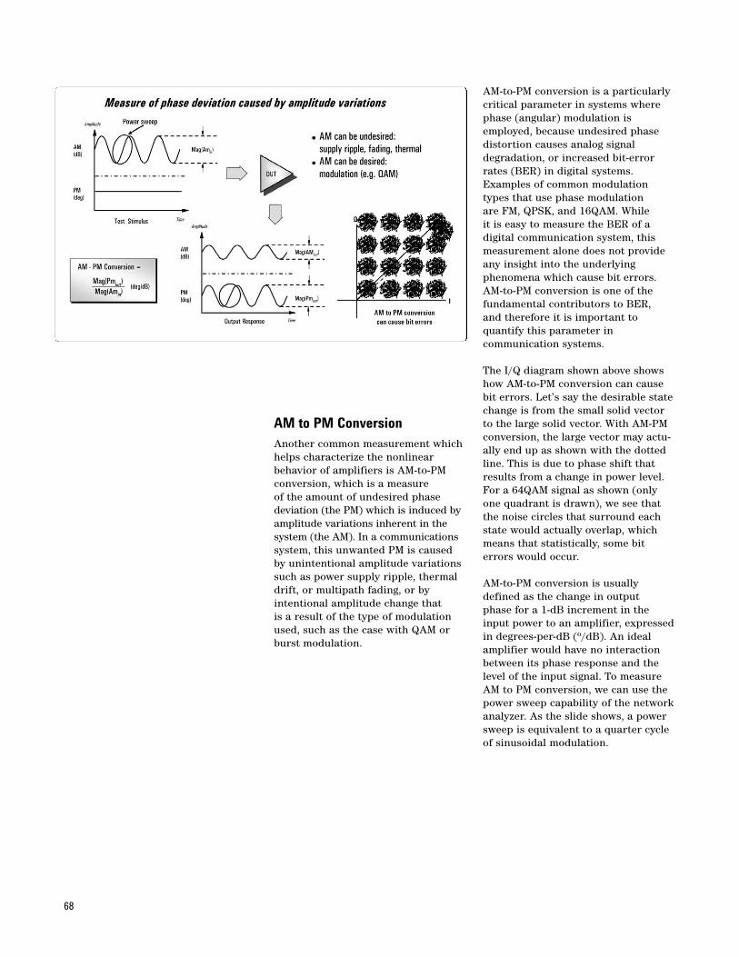
68
AM to PM ConversionAnother common measurement whichhelps characterize the nonlinearbehavior of amplifiers is AM-to-PMconversion, which is a measure of the amount of undesired phasedeviation (the PM) which is induced byamplitude variations inherent in thesystem (the AM). In a communicationssystem, this unwanted PM is causedby unintentional amplitude variationssuch as power supply ripple, thermaldrift, or multipath fading, or by intentional amplitude change that is a result of the type of modulationused, such as the case with QAM orburst modulation.
AM-to-PM conversion is a particularlycritical parameter in systems wherephase (angular) modulation isemployed, because undesired phasedistortion causes analog signal degradation, or increased bit-errorrates (BER) in digital systems.Examples of common modulationtypes that use phase modulation are FM, QPSK, and 16QAM. While it is easy to measure the BER of a digital communication system, thismeasurement alone does not provideany insight into the underlying phenomena which cause bit errors.AM-to-PM conversion is one of thefundamental contributors to BER, and therefore it is important to quantify this parameter in communication systems.
The I/Q diagram shown above showshow AM-to-PM conversion can causebit errors. Let’s say the desirable statechange is from the small solid vectorto the large solid vector. With AM-PMconversion, the large vector may actu-ally end up as shown with the dottedline. This is due to phase shift thatresults from a change in power level.For a 64QAM signal as shown (onlyone quadrant is drawn), we see thatthe noise circles that surround eachstate would actually overlap, whichmeans that statistically, some biterrors would occur.
AM-to-PM conversion is usuallydefined as the change in output phase for a 1-dB increment in theinput power to an amplifier, expressedin degrees-per-dB (o/dB). An idealamplifier would have no interactionbetween its phase response and thelevel of the input signal. To measureAM to PM conversion, we can use thepower sweep capability of the networkanalyzer. As the slide shows, a powersweep is equivalent to a quarter cycleof sinusoidal modulation.
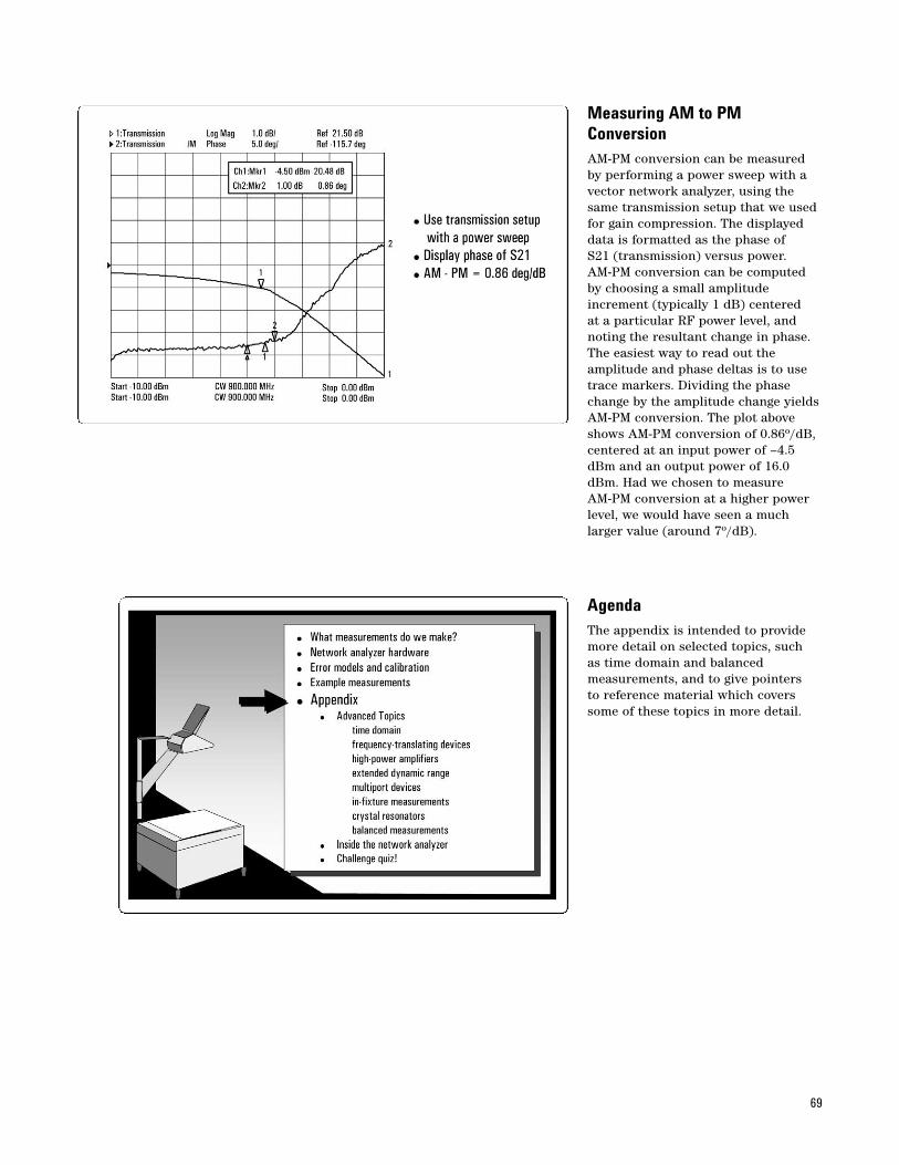
69
Measuring AM to PMConversionAM-PM conversion can be measuredby performing a power sweep with avector network analyzer, using thesame transmission setup that we usedfor gain compression. The displayeddata is formatted as the phase of S21 (transmission) versus power. AM-PM conversion can be computedby choosing a small amplitude increment (typically 1 dB) centered at a particular RF power level, andnoting the resultant change in phase.The easiest way to read out the amplitude and phase deltas is to usetrace markers. Dividing the phasechange by the amplitude change yieldsAM-PM conversion. The plot aboveshows AM-PM conversion of 0.86o/dB,centered at an input power of –4.5dBm and an output power of 16.0dBm. Had we chosen to measure AM-PM conversion at a higher powerlevel, we would have seen a much larger value (around 7o/dB).
AgendaThe appendix is intended to providemore detail on selected topics, such as time domain and balanced measurements, and to give pointers to reference material which coverssome of these topics in more detail.
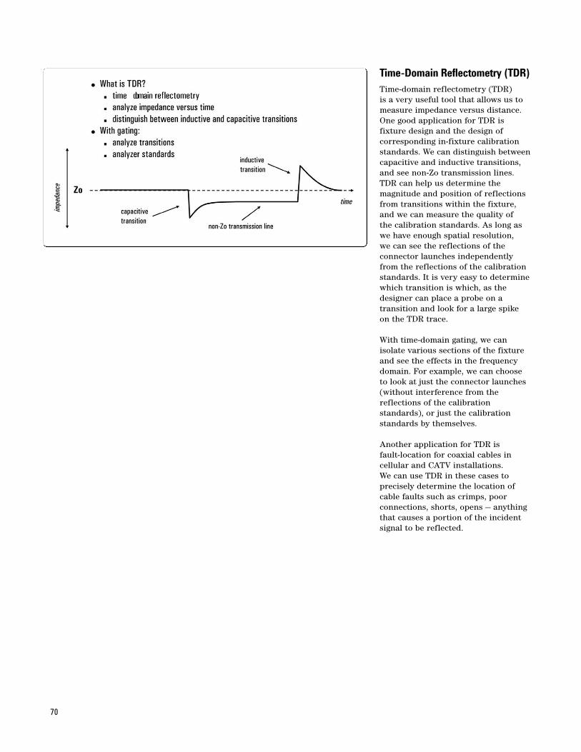
70
Time-Domain Reflectometry (TDR)Time-domain reflectometry (TDR) is a very useful tool that allows us tomeasure impedance versus distance.One good application for TDR is fixture design and the design of corresponding in-fixture calibrationstandards. We can distinguish betweencapacitive and inductive transitions,and see non-Zo transmission lines.TDR can help us determine the magnitude and position of reflectionsfrom transitions within the fixture,and we can measure the quality of the calibration standards. As long aswe have enough spatial resolution, we can see the reflections of the connector launches independentlyfrom the reflections of the calibrationstandards. It is very easy to determinewhich transition is which, as thedesigner can place a probe on a transition and look for a large spikeon the TDR trace.
With time-domain gating, we can isolate various sections of the fixtureand see the effects in the frequencydomain. For example, we can chooseto look at just the connector launches(without interference from the reflections of the calibration standards), or just the calibrationstandards by themselves.
Another application for TDR is fault-location for coaxial cables in cellular and CATV installations. We can use TDR in these cases to precisely determine the location ofcable faults such as crimps, poor connections, shorts, opens — anythingthat causes a portion of the incidentsignal to be reflected.
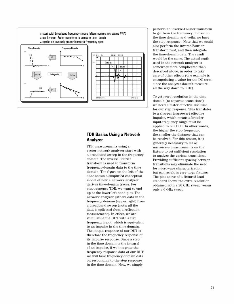
71
TDR Basics Using a NetworkAnalyzerTDR measurements using a vector network analyzer start with a broadband sweep in the frequencydomain. The inverse-Fourier transform is used to transform frequency-domain data to the timedomain. The figure on the left of theslide shows a simplified conceptualmodel of how a network analyzerderives time-domain traces. For step-response TDR, we want to end up at the lower left-hand plot. The network analyzer gathers data in thefrequency domain (upper right) from a broadband sweep (note: all the data is collected from a reflectionmeasurement). In effect, we are stimulating the DUT with a flat frequency input, which is equivalentto an impulse in the time domain. The output response of our DUT istherefore the frequency response of its impulse response. Since a step in the time domain is the integral of an impulse, if we integrate the frequency-response data of our DUT,we will have frequency-domain datacorresponding to the step response in the time domain. Now, we simply
perform an inverse-Fourier transformto get from the frequency domain tothe time domain, and voilá, we havethe step response . Note that we couldalso perform the inverse-Fouriertransform first, and then integrate the time-domain data. The resultwould be the same. The actual mathused in the network analyzer is somewhat more complicated thandescribed above, in order to take care of other effects (one example isextrapolating a value for the DC term,since the analyzer doesn’t measure all the way down to 0 Hz).
To get more resolution in the timedomain (to separate transitions), we need a faster effective rise time for our step response. This translatesto a sharper (narrower) effectiveimpulse, which means a broaderinput-frequency range must be applied to our DUT. In other words,the higher the stop frequency, the smaller the distance that can be resolved. For this reason, it is generally necessary to makemicrowave measurements on the fixture to get sufficient resolution to analyze the various transitions.Providing sufficient spacing betweentransitions may eliminate the need for microwave characterization, but can result in very large fixtures.The plot above of a fixtured-load standard shows the extra resolutionobtained with a 20 GHz sweep versusonly a 6 GHz sweep.
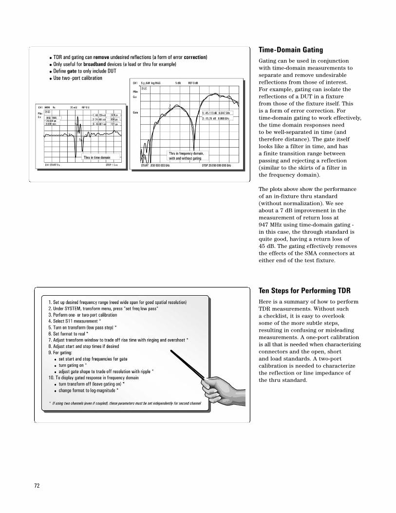
72
Time-Domain GatingGating can be used in conjunctionwith time-domain measurements toseparate and remove undesirablereflections from those of interest. For example, gating can isolate thereflections of a DUT in a fixture from those of the fixture itself. This is a form of error correction. For time-domain gating to work effectively,the time domain responses need to be well-separated in time (andtherefore distance). The gate itselflooks like a filter in time, and has a finite transition range between passing and rejecting a reflection(similar to the skirts of a filter in the frequency domain).
The plots above show the performanceof an in-fixture thru standard (without normalization). We see about a 7 dB improvement in themeasurement of return loss at 947 MHz using time-domain gating - in this case, the through standard isquite good, having a return loss of 45 dB. The gating effectively removesthe effects of the SMA connectors ateither end of the test fixture.
Ten Steps for Performing TDRHere is a summary of how to performTDR measurements. Without such a checklist, it is easy to overlook some of the more subtle steps, resulting in confusing or misleadingmeasurements. A one-port calibrationis all that is needed when characterizingconnectors and the open, short and load standards. A two-port calibration is needed to characterizethe reflection or line impedance of the thru standard.
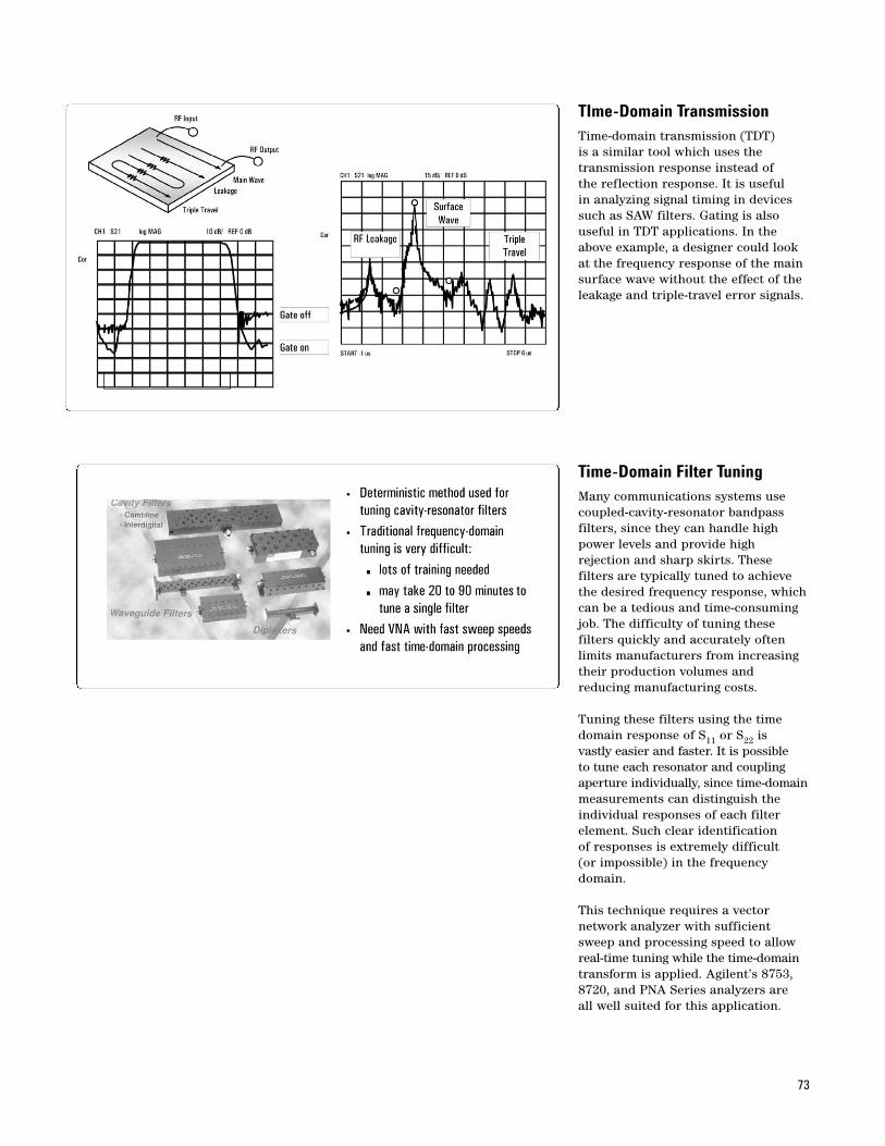
73
TIme-Domain TransmissionTime-domain transmission (TDT) is a similar tool which uses the transmission response instead of the reflection response. It is useful in analyzing signal timing in devicessuch as SAW filters. Gating is also useful in TDT applications. In theabove example, a designer could lookat the frequency response of the mainsurface wave without the effect of theleakage and triple-travel error signals.
Time-Domain Filter TuningMany communications systems usecoupled-cavity-resonator bandpass filters, since they can handle highpower levels and provide high rejection and sharp skirts. These filters are typically tuned to achievethe desired frequency response, whichcan be a tedious and time-consumingjob. The difficulty of tuning these filters quickly and accurately oftenlimits manufacturers from increasingtheir production volumes and reducing manufacturing costs.
Tuning these filters using the timedomain response of S11 or S22 is vastly easier and faster. It is possible to tune each resonator and couplingaperture individually, since time-domainmeasurements can distinguish theindividual responses of each filter element. Such clear identification of responses is extremely difficult (or impossible) in the frequencydomain.
This technique requires a vector network analyzer with sufficientsweep and processing speed to allowreal-time tuning while the time-domaintransform is applied. Agilent’s 8753,8720, and PNA Series analyzers are all well suited for this application.
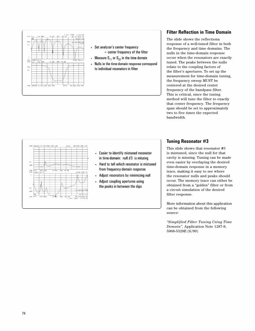
74
Filter Reflection in Time DomainThe slide shows the reflectionaresponse of a well-tuned filter in boththe frequency and time domains. Thenulls in the time-domain responseoccur when the resonators are exactlytuned. The peaks between the nullsrelate to the coupling factors of the filter’s apertures. To set up themeasurement for time-domain tuning,the frequency sweep MUST be centered at the desired center frequency of the bandpass filter. This is critical, since the tuningmethod will tune the filter to exactlythat center frequency. The frequencyspan should be set to approximatelytwo to five times the expected bandwidth.
Tuning Resonator #3This slide shows that resonator #3 is mistuned, since the null for thatcavity is missing. Tuning can be madeeven easier by overlaying the desiredtime-domain response in a memorytrace, making it easy to see where the resonator nulls and peaks shouldoccur. The memory trace can either beobtained from a “golden” filter or froma circuit simulation of the desired filter response.
More information about this applicationcan be obtained from the followingsource:
“Simplified Filter Tuning Using TimeDomain”, Application Note 1287-8,5968-5328E (6/99)
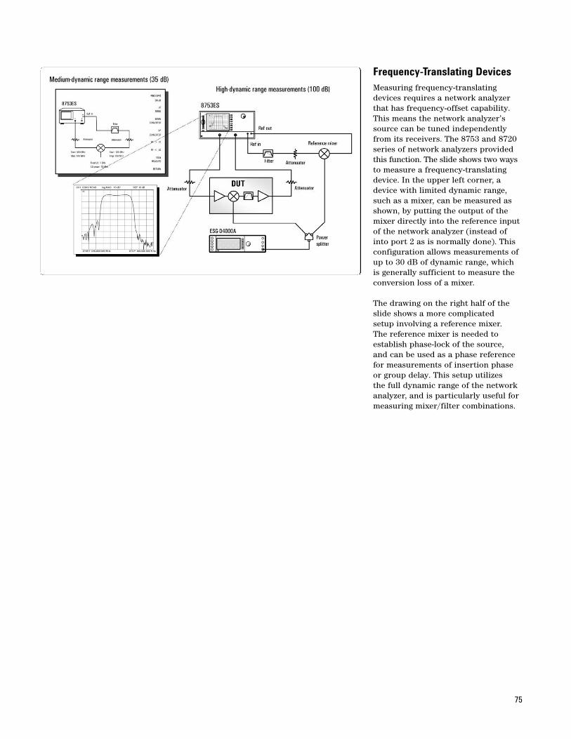
75
Frequency-Translating DevicesMeasuring frequency-translatingdevices requires a network analyzerthat has frequency-offset capability.This means the network analyzer’ssource can be tuned independentlyfrom its receivers. The 8753 and 8720series of network analyzers providedthis function. The slide shows two waysto measure a frequency-translatingdevice. In the upper left corner, adevice with limited dynamic range,such as a mixer, can be measured asshown, by putting the output of themixer directly into the reference inputof the network analyzer (instead ofinto port 2 as is normally done). Thisconfiguration allows measurements ofup to 30 dB of dynamic range, whichis generally sufficient to measure theconversion loss of a mixer.
The drawing on the right half of theslide shows a more complicated setup involving a reference mixer. The reference mixer is needed toestablish phase-lock of the source, and can be used as a phase referencefor measurements of insertion phaseor group delay. This setup utilizes the full dynamic range of the networkanalyzer, and is particularly useful formeasuring mixer/filter combinations.
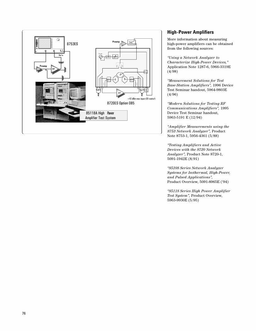
76
High-Power AmplifiersMore information about measuringhigh-power amplifiers can be obtainedfrom the following sources:
“Using a Network Analyzer toCharacterize High-Power Devices,”Application Note 1287-6, 5966-3319E(4/98)
“Measurement Solutions for Test Base-Station Amplifiers”, 1996 DeviceTest Seminar handout, 5964-9803E(4/96)
“Modern Solutions for Testing RFCommunications Amplifiers”, 1995Device Test Seminar handout, 5963-5191 E (12/94)
“Amplifier Measurements using the8753 Network Analyzer”, ProductNote 8753-1, 5956-4361 (5/88)
“Testing Amplifiers and ActiveDevices with the 8720 NetworkAnalyzer”, Product Note 8720-1, 5091-1942E (8/91)
“85108 Series Network AnalyzerSystems for Isothermal, High-Power,and Pulsed Applications”,Product Overview, 5091-8965E (‘94)
“85118 Series High Power AmplifierTest System”, Product Overview, 5963-9930E (5/95)
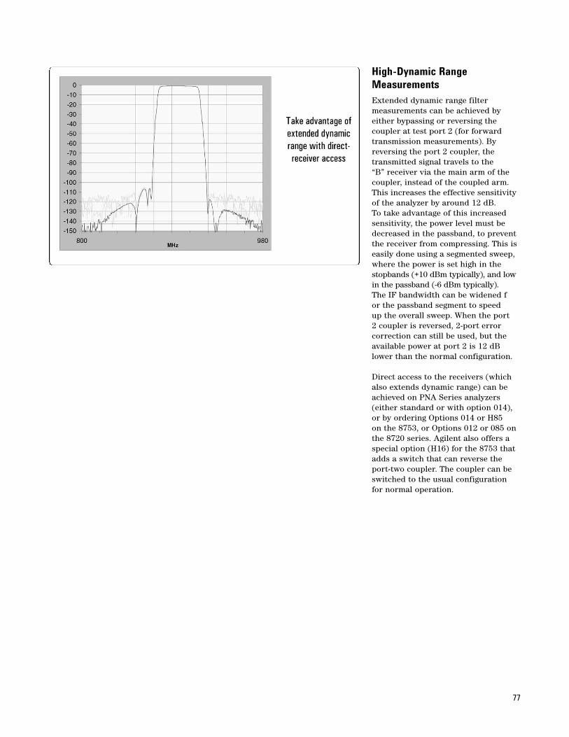
77
High-Dynamic RangeMeasurementsExtended dynamic range filter measurements can be achieved byeither bypassing or reversing the coupler at test port 2 (for forwardtransmission measurements). Byreversing the port 2 coupler, the transmitted signal travels to the “B” receiver via the main arm of thecoupler, instead of the coupled arm.This increases the effective sensitivityof the analyzer by around 12 dB. To take advantage of this increasedsensitivity, the power level must bedecreased in the passband, to preventthe receiver from compressing. This iseasily done using a segmented sweep,where the power is set high in thestopbands (+10 dBm typically), and lowin the passband (-6 dBm typically).The IF bandwidth can be widened for the passband segment to speed up the overall sweep. When the port 2 coupler is reversed, 2-port error correction can still be used, but theavailable power at port 2 is 12 dBlower than the normal configuration.
Direct access to the receivers (whichalso extends dynamic range) can beachieved on PNA Series analyzers(either standard or with option 014),or by ordering Options 014 or H85 on the 8753, or Options 012 or 085 onthe 8720 series. Agilent also offers aspecial option (H16) for the 8753 thatadds a switch that can reverse theport-two coupler. The coupler can beswitched to the usual configurationfor normal operation.
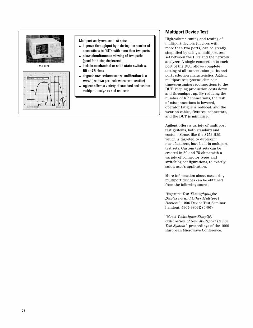
78
Multiport Device TestHigh-volume tuning and testing ofmultiport devices (devices with more than two ports) can be greatlysimplified by using a multiport test set between the DUT and the networkanalyzer. A single connection to eachport of the DUT allows complete testing of all transmission paths andport reflection characteristics. Agilentmultiport test systems eliminatetime-consuming reconnections to theDUT, keeping production costs downand throughput up. By reducing thenumber of RF connections, the risk of misconnections is lowered, operator fatigue is reduced, and thewear on cables, fixtures, connectors,and the DUT is minimized.
Agilent offers a variety of multiporttest systems, both standard and custom. Some, like the 8753 H39,which is targeted to duplexer manufacturers, have built-in multiporttest sets. Custom test sets can be created in 50 and 75 ohms with a variety of connector types and switching configurations, to exactlysuit a user’s application.
More information about measuringmultiport devices can be obtainedfrom the following source:
“Improve Test Throughput forDuplexers and Other MultiportDevices”, 1996 Device Test Seminarhandout, 5964-9803E (4/96)
“Novel Techniques SimplifyCalibration of New Multiport DeviceTest System”, proceedings of the 1999European Microwave Conference.
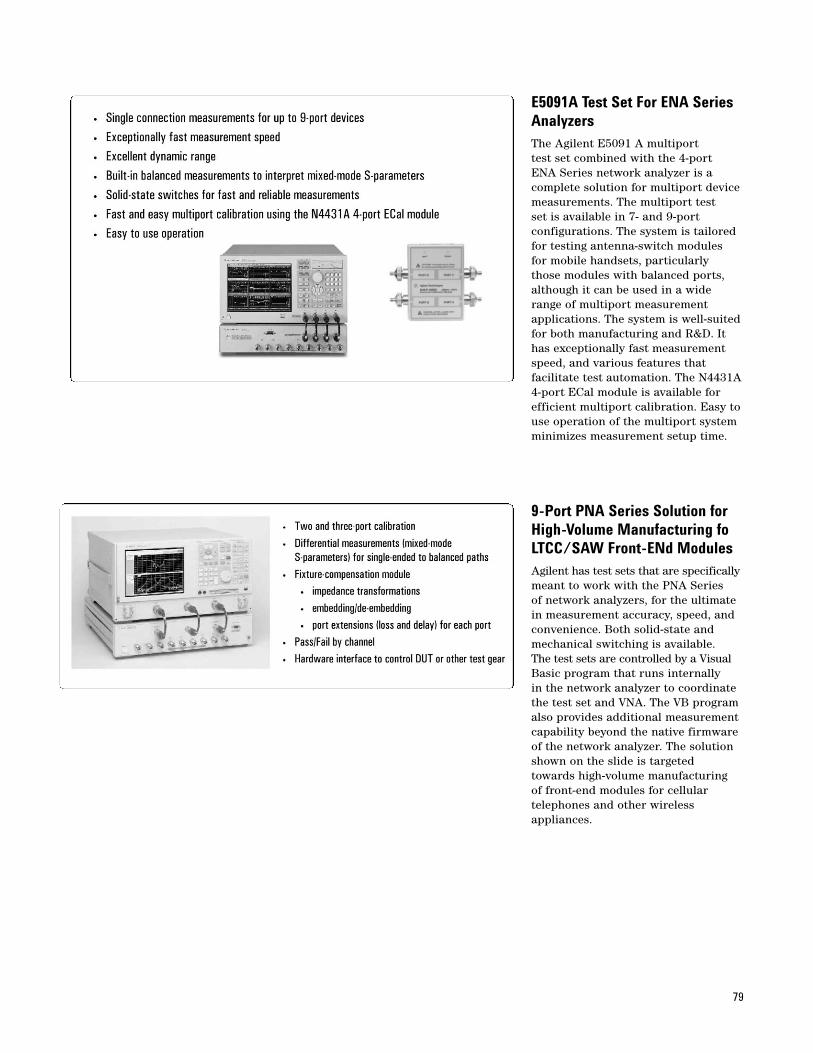
79
E5091A Test Set For ENA SeriesAnalyzersThe Agilent E5091 A multiport test set combined with the 4-port ENA Series network analyzer is a complete solution for multiport devicemeasurements. The multiport test set is available in 7- and 9-port configurations. The system is tailoredfor testing antenna-switch modules for mobile handsets, particularly those modules with balanced ports,although it can be used in a widerange of multiport measurementapplications. The system is well-suitedfor both manufacturing and R&D. Ithas exceptionally fast measurementspeed, and various features that facilitate test automation. The N4431A4-port ECal module is available forefficient multiport calibration. Easy touse operation of the multiport systemminimizes measurement setup time.
9-Port PNA Series Solution forHigh-Volume Manufacturing foLTCC/SAW Front-ENd ModulesAgilent has test sets that are specificallymeant to work with the PNA Series of network analyzers, for the ultimatein measurement accuracy, speed, andconvenience. Both solid-state andmechanical switching is available. The test sets are controlled by a VisualBasic program that runs internally in the network analyzer to coordinatethe test set and VNA. The VB programalso provides additional measurementcapability beyond the native firmwareof the network analyzer. The solutionshown on the slide is targeted towards high-volume manufacturing of front-end modules for cellular telephones and other wireless appliances.
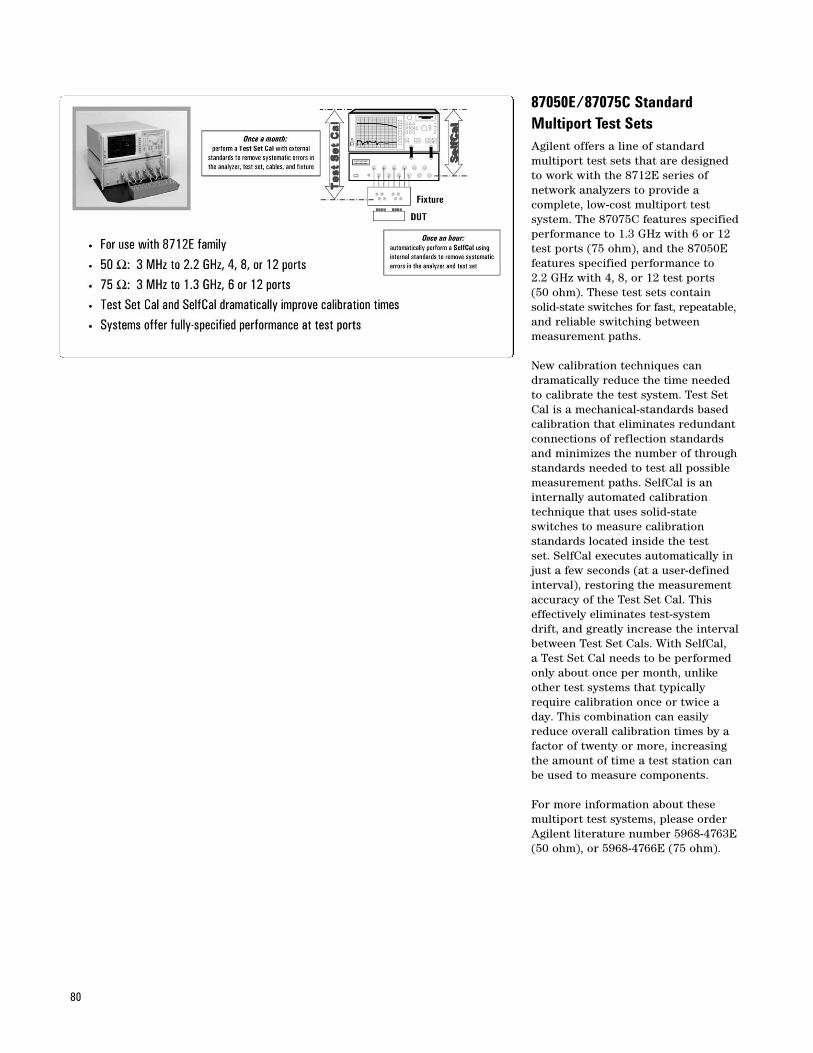
80
87050E/87075C StandardMultiport Test SetsAgilent offers a line of standard multiport test sets that are designedto work with the 8712E series of network analyzers to provide a complete, low-cost multiport test system. The 87075C features specifiedperformance to 1.3 GHz with 6 or 12test ports (75 ohm), and the 87050Efeatures specified performance to 2.2 GHz with 4, 8, or 12 test ports (50 ohm). These test sets containsolid-state switches for fast, repeatable,and reliable switching between measurement paths.
New calibration techniques can dramatically reduce the time neededto calibrate the test system. Test SetCal is a mechanical-standards basedcalibration that eliminates redundantconnections of reflection standardsand minimizes the number of throughstandards needed to test all possiblemeasurement paths. SelfCal is aninternally automated calibration technique that uses solid-state switches to measure calibration standards located inside the test set. SelfCal executes automatically injust a few seconds (at a user-definedinterval), restoring the measurementaccuracy of the Test Set Cal. Thiseffectively eliminates test-system drift, and greatly increase the intervalbetween Test Set Cals. With SelfCal, a Test Set Cal needs to be performedonly about once per month, unlikeother test systems that typicallyrequire calibration once or twice aday. This combination can easilyreduce overall calibration times by afactor of twenty or more, increasingthe amount of time a test station canbe used to measure components.
For more information about thesemultiport test systems, please orderAgilent literature number 5968-4763E(50 ohm), or 5968-4766E (75 ohm).
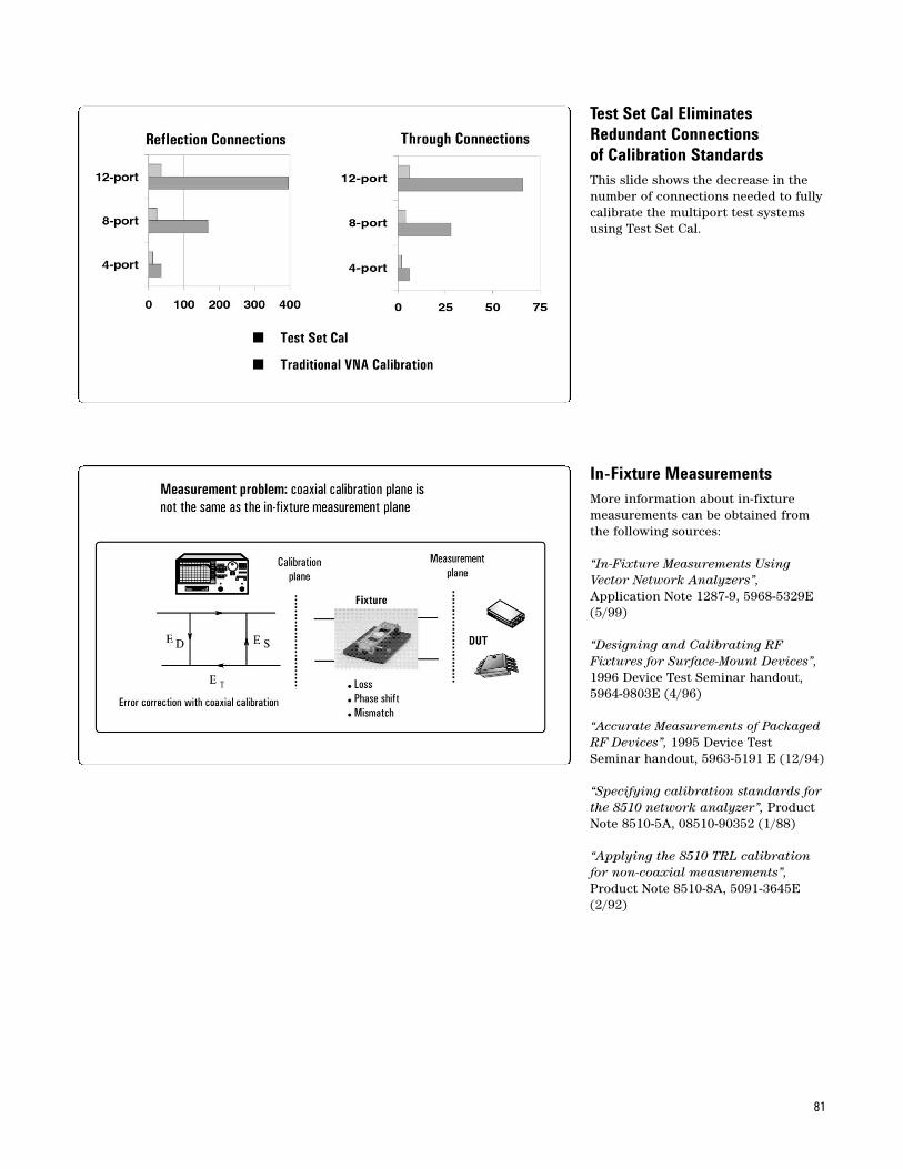
81
In-Fixture MeasurementsMore information about in-fixturemeasurements can be obtained fromthe following sources:
“In-Fixture Measurements UsingVector Network Analyzers”,Application Note 1287-9, 5968-5329E(5/99)
“Designing and Calibrating RFFixtures for Surface-Mount Devices”,1996 Device Test Seminar handout,5964-9803E (4/96)
“Accurate Measurements of PackagedRF Devices”, 1995 Device TestSeminar handout, 5963-5191 E (12/94)
“Specifying calibration standards forthe 8510 network analyzer”, ProductNote 8510-5A, 08510-90352 (1/88)
“Applying the 8510 TRL calibrationfor non-coaxial measurements”,Product Note 8510-8A, 5091-3645E(2/92)
Test Set Cal EliminatesRedundant Connectionsof Calibration StandardsThis slide shows the decrease in thenumber of connections needed to fullycalibrate the multiport test systemsusing Test Set Cal.
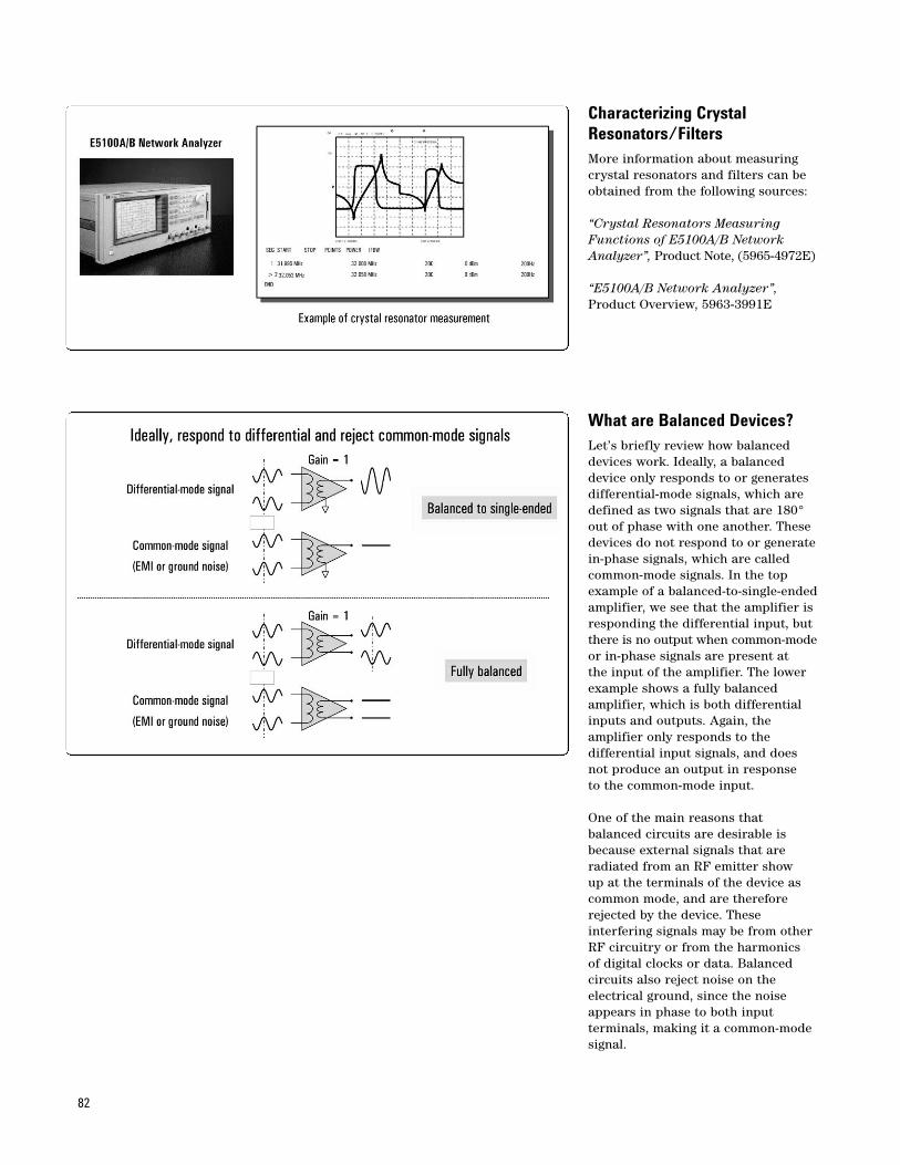
82
What are Balanced Devices?Let’s briefly review how balanceddevices work. Ideally, a balanceddevice only responds to or generatesdifferential-mode signals, which aredefined as two signals that are 180°out of phase with one another. Thesedevices do not respond to or generatein-phase signals, which are calledcommon-mode signals. In the topexample of a balanced-to-single-endedamplifier, we see that the amplifier isresponding the differential input, butthere is no output when common-modeor in-phase signals are present at the input of the amplifier. The lowerexample shows a fully balanced amplifier, which is both differentialinputs and outputs. Again, the amplifier only responds to the differential input signals, and does not produce an output in response to the common-mode input.
One of the main reasons that balanced circuits are desirable isbecause external signals that are radiated from an RF emitter show up at the terminals of the device ascommon mode, and are thereforerejected by the device. These interfering signals may be from otherRF circuitry or from the harmonics of digital clocks or data. Balanced circuits also reject noise on the electrical ground, since the noiseappears in phase to both input terminals, making it a common-modesignal.
Characterizing CrystalResonators/FiltersMore information about measuringcrystal resonators and filters can beobtained from the following sources:
“Crystal Resonators MeasuringFunctions of E5100A/B NetworkAnalyzer”, Product Note, (5965-4972E)
“E5100A/B Network Analyzer”,Product Overview, 5963-3991E
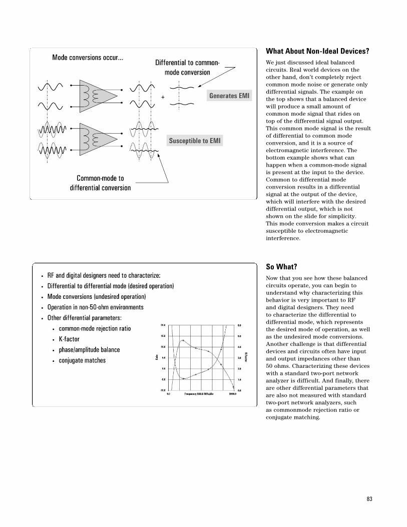
83
So What?Now that you see how these balancedcircuits operate, you can begin tounderstand why characterizing thisbehavior is very important to RF and digital designers. They need to characterize the differential to differential mode, which representsthe desired mode of operation, as wellas the undesired mode conversions.Another challenge is that differentialdevices and circuits often have inputand output impedances other than 50 ohms. Characterizing these deviceswith a standard two-port network analyzer is difficult. And finally, thereare other differential parameters thatare also not measured with standardtwo-port network analyzers, such as commonmode rejection ratio orconjugate matching.
What About Non-Ideal Devices?We just discussed ideal balanced circuits. Real world devices on theother hand, don’t completely rejectcommon mode noise or generate onlydifferential signals. The example onthe top shows that a balanced devicewill produce a small amount of common mode signal that rides on top of the differential signal output.This common mode signal is the resultof differential to common mode conversion, and it is a source of electromagnetic interference. The bottom example shows what can happen when a common-mode signalis present at the input to the device.Common to differential mode conversion results in a differential signal at the output of the device,which will interfere with the desireddifferential output, which is notshown on the slide for simplicity. This mode conversion makes a circuitsusceptible to electromagnetic interference.
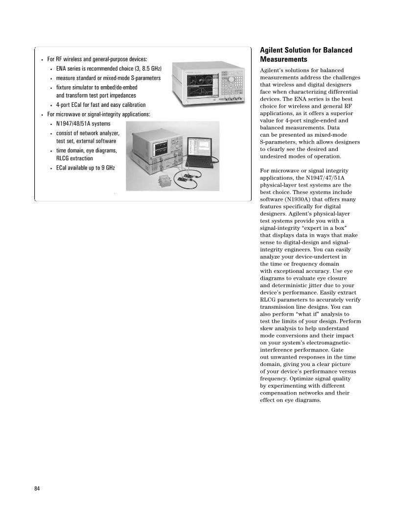
84
Agilent Solution for BalancedMeasurementsAgilent’s solutions for balanced measurements address the challengesthat wireless and digital designersface when characterizing differentialdevices. The ENA series is the bestchoice for wireless and general RFapplications, as it offers a superiorvalue for 4-port single-ended and balanced measurements. Data can be presented as mixed-mode S-parameters, which allows designersto clearly see the desired and undesired modes of operation.
For microwave or signal integrityapplications, the N1947/47/51A physical-layer test systems are thebest choice. These systems includesoftware (N1930A) that offers manyfeatures specifically for digital designers. Agilent’s physical-layer test systems provide you with a signal-integrity “expert in a box” that displays data in ways that makesense to digital-design and signal-integrity engineers. You can easilyanalyze your device-undertest in the time or frequency domain with exceptional accuracy. Use eyediagrams to evaluate eye closure and deterministic jitter due to yourdevice’s performance. Easily extractRLCG parameters to accurately verifytransmission line designs. You canalso perform “what if” analysis to test the limits of your design. Performskew analysis to help understandmode conversions and their impact on your system’s electromagnetic-interference performance. Gate out unwanted responses in the timedomain, giving you a clear picture of your device’s performance versusfrequency. Optimize signal quality by experimenting with different compensation networks and theireffect on eye diagrams.
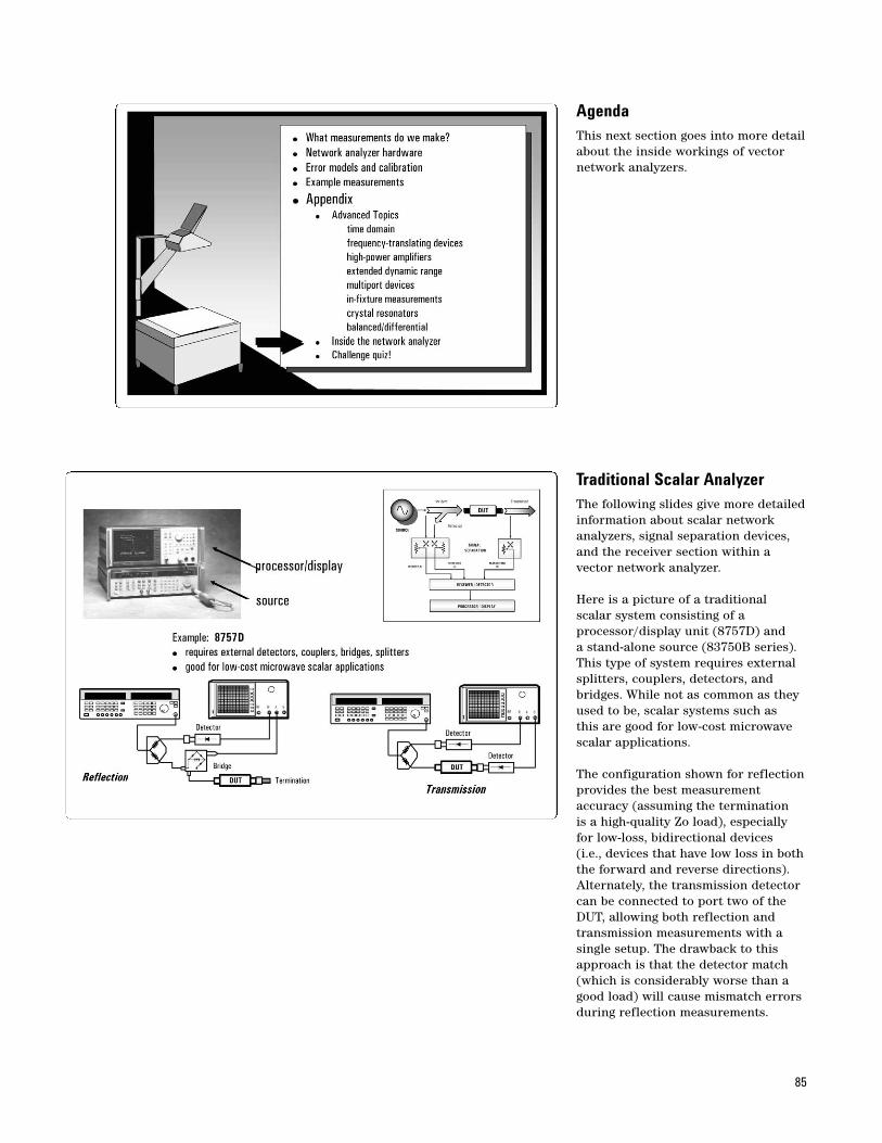
85
AgendaThis next section goes into more detailabout the inside workings of vectornetwork analyzers.
Traditional Scalar AnalyzerThe following slides give more detailedinformation about scalar network analyzers, signal separation devices,and the receiver section within a vector network analyzer.
Here is a picture of a traditionalscalar system consisting of a processor/display unit (8757D) and a stand-alone source (83750B series).This type of system requires externalsplitters, couplers, detectors, andbridges. While not as common as theyused to be, scalar systems such as this are good for low-cost microwavescalar applications.
The configuration shown for reflectionprovides the best measurement accuracy (assuming the termination is a high-quality Zo load), especiallyfor low-loss, bidirectional devices (i.e., devices that have low loss in boththe forward and reverse directions).Alternately, the transmission detectorcan be connected to port two of theDUT, allowing both reflection andtransmission measurements with asingle setup. The drawback to thisapproach is that the detector match(which is considerably worse than agood load) will cause mismatch errorsduring reflection measurements.
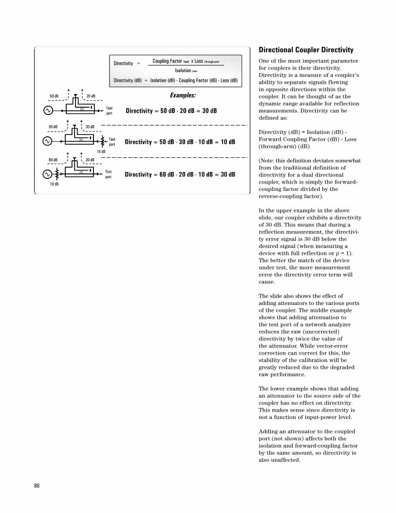
86
Directional Coupler DirectivityOne of the most important parameterfor couplers is their directivity.Directivity is a measure of a coupler’sability to separate signals flowing in opposite directions within the coupler. It can be thought of as thedynamic range available for reflectionmeasurements. Directivity can bedefined as:
Directivity (dB) = Isolation (dB) -Forward Coupling Factor (dB) - Loss(through-arm) (dB)
(Note: this definition deviates somewhatfrom the traditional definition ofdirectivity for a dual directional coupler, which is simply the forward-coupling factor divided by the reverse-coupling factor).
In the upper example in the aboveslide, our coupler exhibits a directivityof 30 dB. This means that during areflection measurement, the directivi-ty error signal is 30 dB below thedesired signal (when measuring adevice with full reflection or ρ = 1).The better the match of the deviceunder test, the more measurementerror the directivity error term willcause.
The slide also shows the effect ofadding attenuators to the various portsof the coupler. The middle exampleshows that adding attenuation to the test port of a network analyzerreduces the raw (uncorrected) directivity by twice the value of the attenuator. While vector-error correction can correct for this, the stability of the calibration will begreatly reduced due to the degradedraw performance.
The lower example shows that addingan attenuator to the source side of thecoupler has no effect on directivity.This makes sense since directivity isnot a function of input-power level.
Adding an attenuator to the coupledport (not shown) affects both the isolation and forward-coupling factorby the same amount, so directivity isalso unaffected.
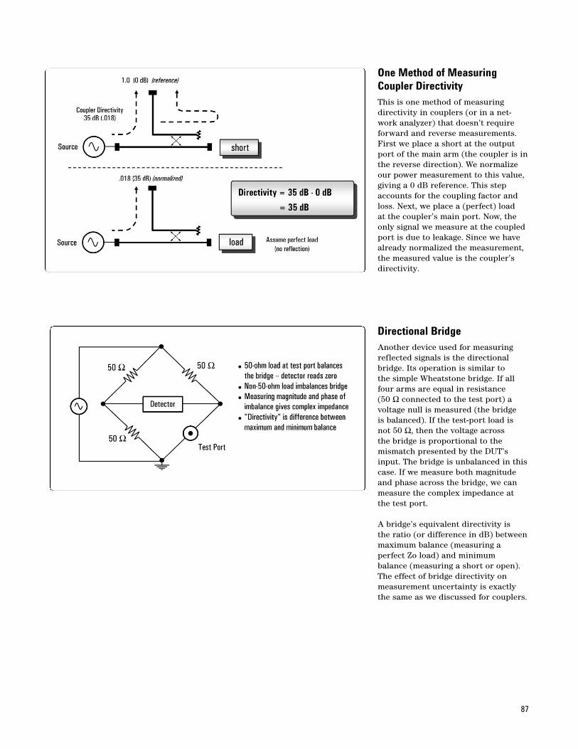
87
Directional BridgeAnother device used for measuringreflected signals is the directionalbridge. Its operation is similar to the simple Wheatstone bridge. If allfour arms are equal in resistance (50 Ω connected to the test port) avoltage null is measured (the bridge is balanced). If the test-port load isnot 50 Ω, then the voltage across the bridge is proportional to the mismatch presented by the DUT’sinput. The bridge is unbalanced in thiscase. If we measure both magnitudeand phase across the bridge, we canmeasure the complex impedance atthe test port.
A bridge’s equivalent directivity is the ratio (or difference in dB) betweenmaximum balance (measuring a perfect Zo load) and minimum balance (measuring a short or open).The effect of bridge directivity onmeasurement uncertainty is exactlythe same as we discussed for couplers.
One Method of MeasuringCoupler DirectivityThis is one method of measuringdirectivity in couplers (or in a net-work analyzer) that doesn’t requireforward and reverse measurements.First we place a short at the outputport of the main arm (the coupler is inthe reverse direction). We normalizeour power measurement to this value,giving a 0 dB reference. This stepaccounts for the coupling factor andloss. Next, we place a (perfect) load at the coupler’s main port. Now, theonly signal we measure at the coupledport is due to leakage. Since we havealready normalized the measurement,the measured value is the coupler’sdirectivity.
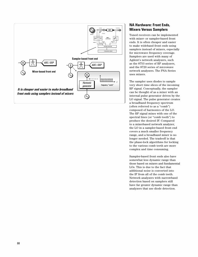
88
NA Hardware: Front Ends, Mixers Versus SamplersTuned receivers can be implementedwith mixer- or sampler-based frontends. It is often cheaper and easier to make wideband front ends usingsamplers instead of mixers, especiallyfor microwave frequency coverage.Samplers are used with many ofAgilent’s network analyzers, such as the 8753 series of RF analyzers,and the 8720 series of microwave network analyzers. The PNA Seriesuses mixers.
The sampler uses diodes to samplevery short time slices of the incomingRF signal. Conceptually, the samplercan be thought of as a mixer with aninternal pulse generator driven by theLO signal. The pulse generator createsa broadband frequency spectrum(often referred to as a “comb”) composed of harmonics of the LO. The RF signal mixes with one of thespectral lines (or “comb tooth”) toproduce the desired IF. Compared to a mixerbased network analyzer, the LO in a sampler-based front endcovers a much smaller frequencyrange, and a broadband mixer is nolonger needed. The tradeoff is that the phase-lock algorithms for lockingto the various comb teeth are morecomplex and time consuming.
Sampler-based front ends also havesomewhat less dynamic range thanthose based on mixers and fundamentalLOs. This is due to the fact that additional noise is converted into the IF from all of the comb teeth.Network analyzers with narrowbanddetection based on samplers still have far greater dynamic range thananalyzers that use diode detection.
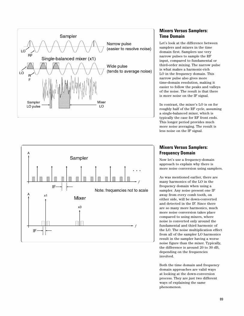
89
Mixers Versus Samplers: Time DomainLet’s look at the difference betweensamplers and mixers in the timedomain first. Samplers use very narrow pulses to sample the RF input, compared to fundamental orthird-order mixing. The narrow pulseis what makes a harmonic-rich LO in the frequency domain. This narrow pulse also gives more time-domain resolution, making it easier to follow the peaks and valleysof the noise. The result is that there is more noise on the IF signal.
In contrast, the mixer’s LO is on forroughly half of the RF cycle, assuminga single-balanced mixer, which is typically the case for RF front ends.This longer period provides muchmore noise averaging. The result isless noise on the IF signal.
Mixers Versus Samplers:Frequency DomainNow let’s use a frequency-domainapproach to explain why there is more noise conversion using samplers.
As was mentioned earlier, there aremany harmonics of the LO in the frequency domain when using a sampler. Any noise present one IFaway from every comb tooth, on either side, will be down-convertedand detected in the IF. Since there are so many more harmonics, muchmore noise conversion takes placecompared to using mixers, wherenoise is converted only around thefundamental and third harmonic ofthe LO. The noise multiplication effectfrom all of the sampler LO harmonicsresult in the sampler having a worsenoise figure than the mixer. Typically,the difference is around 20 to 30 dB,depending on the frequenciesinvolved.
Both the time domain and frequencydomain approaches are valid ways at looking at the down-conversionprocess. They are just two differentways of explaining the same phenomenon.
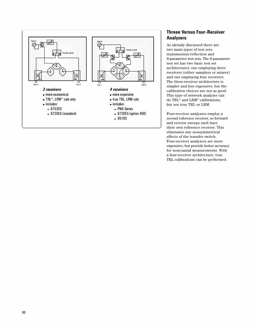
90
Threee Versus Four-ReceiverAnalyzersAs already discussed there are two main types of test sets, transmission/reflection and S-parameter test sets. The S-parametertest set has two basic test set architectures: one employing threereceivers (either samplers or mixers)and one employing four receivers. The three-receiver architecture is simpler and less expensive, but thecalibration choices are not as good.This type of network analyzer can do TRL* and LRM* calibrations, but not true TRL or LRM.
Four-receiver analyzers employ a second reference receiver, so forwardand reverse sweeps each have their own reference receiver. Thiseliminates any nonsymmetrical effects of the transfer switch. Four-receiver analyzers are moreexpensive, but provide better accuracyfor noncoaxial measurements. With a four-receiver architecture, true TRL calibrations can be performed.
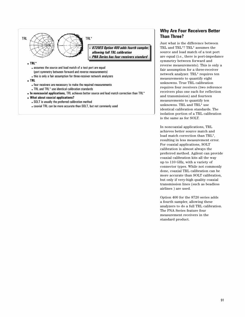
91
Why Are Four Receivers BetterThan Three?Just what is the difference betweenTRL and TRL*? TRL* assumes thesource and load match of a test portare equal (i.e., there is port-impedancesymmetry between forward andreverse measurements). This is only afair assumption for a three-receivernetwork analyzer. TRL* requires tenmeasurements to quantify eightunknowns. True TRL calibrationrequires four receivers (two referencereceivers plus one each for reflectionand transmission) and fourteen measurements to quantify tenunknowns. TRL and TRL* use identical calibration standards. Theisolation portion of a TRL calibrationis the same as for SOLT.
In noncoaxial applications, TRLachieves better source match and load match correction than TRL*,resulting in less measurement error.For coaxial applications, SOLT calibration is almost always the preferred method. Agilent can providecoaxial calibration kits all the way up to 110 GHz, with a variety of connector types. While not commonlydone, coaxial TRL calibration can bemore accurate than SOLT calibration,but only if very-high quality coaxialtransmission lines (such as beadlessairlines ) are used.
Option 400 for the 8720 series adds a fourth sampler, allowing these analyzers to do a full TRL calibration.The PNA Series feature four measurement receivers in the standard product.

92
Challenge Quiz

93
Answers to Challenge QuizThe correct answers to the challengequiz are:1. E2. C3. A4. B5. C6. A7. D8. B
94
Agilent Technologies’ Test and MeasurementSupport, Services, and AssistanceAgilent Technologies aims to maximize the valueyou receive, while minimizing your risk and prob-lems. We strive to ensure that you get the testand measurement capabilities you paid for andobtain the support you need. Our extensive sup-port resources and services can help you choosethe right Agilent products for your applicationsand apply them successfully. Every instrumentand system we sell has a global warranty.Support is available for at least five years beyondthe production life of the product. Two conceptsunderlie Agilent’s overall support policy: “OurPromise” and “Your Advantage.”
Our PromiseOur Promise means your Agilent test and meas-urement equipment will meet its advertisedperformance and functionality. When you arechoosing new equipment, we will help you withproduct information, including realistic perform-ance specifications and practical recommenda-tions from experienced test engineers. When youreceive your new Agilent equipment, we can helpverify that it works properly and help with initialproduct operation.
Your AdvantageYour Advantage means that Agilent offers a wide range of additional expert test and measurement services, which you can purchaseaccording to your unique technical and businessneeds. Solve problems efficiently and gain a competitive edge by contracting with us forcalibration, extra-cost upgrades, out-of-warrantyrepairs, and onsite education and training, as wellas design, system integration, project management,and other professional engineering services.Experienced Agilent engineers and techniciansworldwide can help you maximize your productivity,optimize the return on investment of your Agilentinstruments and systems, and obtain dependablemeasurement accuracy for the life of those products.
www.agilent.com/find/emailupdatesGet the latest information on the products andapplications you select.
Agilent T&M Software and ConnectivityAgilent’s Test and Measurement software andconnectivity products, solutions and developernetwork allows you to take time out of connect-ing your instruments to your computer with toolsbased on PC standards, so you can focus on yourtasks, not on your connections. Visit www.agilent.com/find/connectivityfor more information.
For more information on AgilentTechnologies’ products, applications orservices, please contact your local Agilentoffice. The complete list is available at:
www.agilent.com/find/contactus
Phone or Fax
United States:(tel) 800 829 4444(fax) 800 829 4433
Canada:(tel) 877 894 4414(fax) 905 282 6495
China:(tel) 800 810 0189(fax) 800 820 2816
Europe:(tel) 31 20 547 2111
Japan:(tel) (81) 426 56 7832(fax) (81) 426 56 7840
Korea:(tel) (080) 769 0800(fax) (080)769 0900
Latin America:(tel) (305) 269 7500
Taiwan:(tel) 0800 047 866 (fax) 0800 286 331
Other Asia Pacific Countries:(tel) (65) 6375 8100 (fax) (65) 6755 0042Email: [email protected]
Product specifications and descriptionsin this document subject to changewithout notice.
© Agilent Technologies, Inc. 2004Printed in USA, August 31, 20045965-7917E
Web Sources
For additional information regardingAgilent Network Analyzers, visit:www.agilent.com/find/na
For Agilent “Back To Basics” eSeminar,series information, visit:www.agilent.com/find/backtobasics