Embed Size (px)
Citation preview
RailRail toto RailRail OTAOTARailRail--toto--Rail Rail OTA OTA
1Radivoje Đurić, 2015, Analogna Integrisana Kola
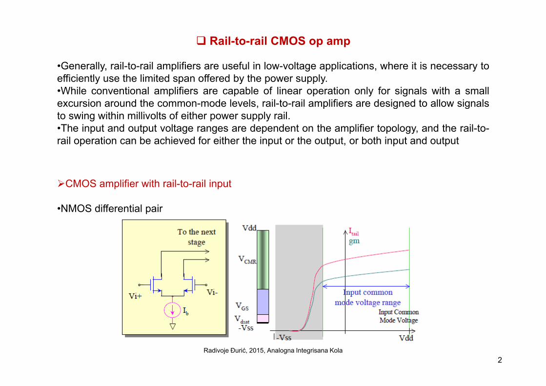
Rail-to-rail CMOS op amp
•Generally, rail-to-rail amplifiers are useful in low-voltage applications, where it is necessary toefficiently use the limited span offered by the power supply.•While conventional amplifiers are capable of linear operation only for signals with a smallexcursion around the common-mode levels rail-to-rail amplifiers are designed to allow signalsexcursion around the common mode levels, rail to rail amplifiers are designed to allow signalsto swing within millivolts of either power supply rail.•The input and output voltage ranges are dependent on the amplifier topology, and the rail-to-rail operation can be achieved for either the input or the output, or both input and output
CMOS amplifier with rail-to-rail input
•NMOS differential pair
Radivoje Đurić, 2015, Analogna Integrisana Kola2

•PMOS differential pair
•PMOS+NMOS differential pair
SGPVDSsatPV
V
2 2
DSsatNV
GSNV
Radivoje Đurić, 2015, Analogna Integrisana Kola3
2 2DD SS THN THP DSsatN DSsatPV V V V V V
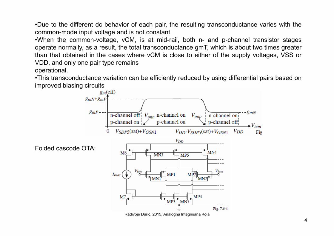
•Due to the different dc behavior of each pair, the resulting transconductance varies with thecommon-mode input voltage and is not constant.Wh th lt CM i t id il b th d h l t i t t•When the common-voltage, vCM, is at mid-rail, both n- and p-channel transistor stages
operate normally, as a result, the total transconductance gmT, which is about two times greaterthan that obtained in the cases where vCM is close to either of the supply voltages, VSS orVDD, and only one pair type remainsVDD, and only one pair type remainsoperational.•This transconductance variation can be efficiently reduced by using differential pairs based onimproved biasing circuits
Folded cascode OTA:
Radivoje Đurić, 2015, Analogna Integrisana Kola4
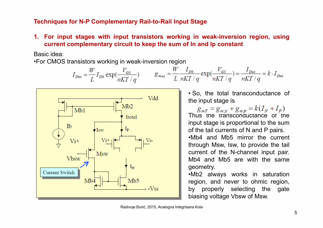
Techniques for N-P Complementary Rail-to-Rail Input Stage
1 For input stages with input transistors working in weak inversion region using1. For input stages with input transistors working in weak-inversion region, usingcurrent complementary circuit to keep the sum of In and Ip constant
Basic idea:•For CMOS transistors working in weak-inversion regionFor CMOS transistors working in weak inversion region
• So, the total transconductance ofthe input stage is
Th th t d t f thThus the transconductance of theinput stage is proportional to the sumof the tail currents of N and P pairs.•Mb4 and Mb5 mirror the currentthrough Msw, Isw, to provide the tailcurrent of the N-channel input pair.Mb4 and Mb5 are with the samegeometrygeometry.•Mb2 always works in saturationregion, and never to ohmic region,by properly selecting the gate
Radivoje Đurić, 2015, Analogna Integrisana Kola5
y p p y g gbiasing voltage Vbsw of Msw.
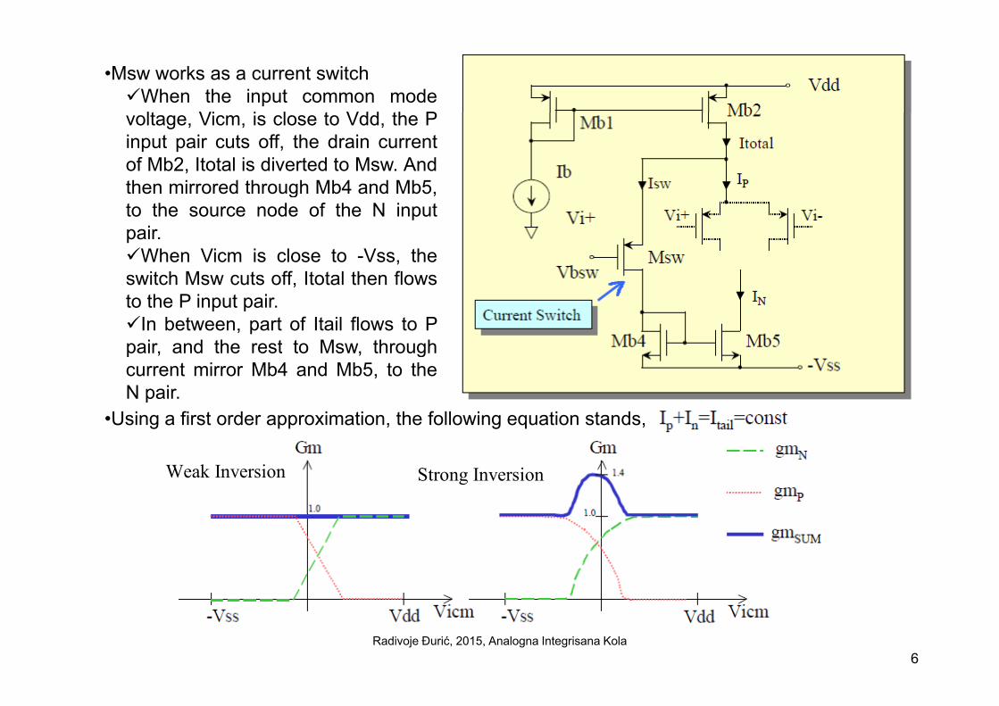
•Msw works as a current switchWhen the input common mode
lt Vi i l t Vdd th Pvoltage, Vicm, is close to Vdd, the Pinput pair cuts off, the drain currentof Mb2, Itotal is diverted to Msw. Andthen mirrored through Mb4 and Mb5,then mirrored through Mb4 and Mb5,to the source node of the N inputpair.When Vicm is close to -Vss, the
it h M t ff It t l th flswitch Msw cuts off, Itotal then flowsto the P input pair.In between, part of Itail flows to Ppair, and the rest to Msw, throughpair, and the rest to Msw, throughcurrent mirror Mb4 and Mb5, to theN pair.
•Using a first order approximation, the following equation stands,
Weak Inversion Strong Inversion
Radivoje Đurić, 2015, Analogna Integrisana Kola6
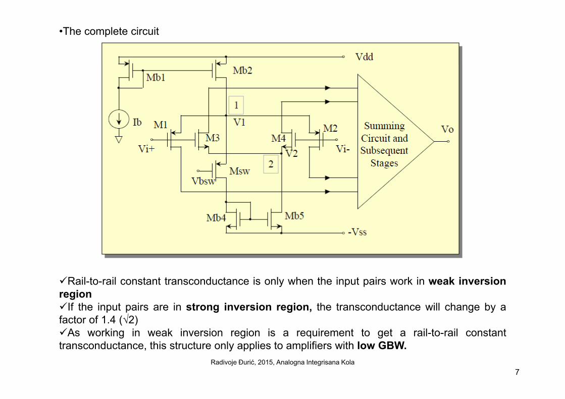
•The complete circuit
Rail-to-rail constant transconductance is only when the input pairs work in weak inversioniregion
If the input pairs are in strong inversion region, the transconductance will change by afactor of 1.4 (√2)As working in weak inversion region is a requirement to get a rail-to-rail constant
Radivoje Đurić, 2015, Analogna Integrisana Kola7
As working in weak inversion region is a requirement to get a rail to rail constanttransconductance, this structure only applies to amplifiers with low GBW.
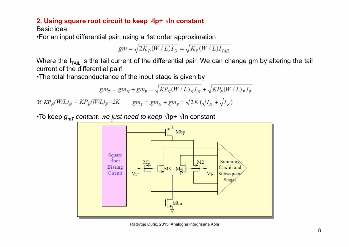
2. Using square root circuit to keep √Ip+ √In constantBasic idea:•For an input differential pair, using a 1st order approximationp p , g pp
Where the ITAIL is the tail current of the differential pair. We can change gm by altering the tailc rrent of the differential pair!current of the differential pair!•The total transconductance of the input stage is given by
•To keep gmT contant, we just need to keep √Ip+ √In constant
Radivoje Đurić, 2015, Analogna Integrisana Kola8
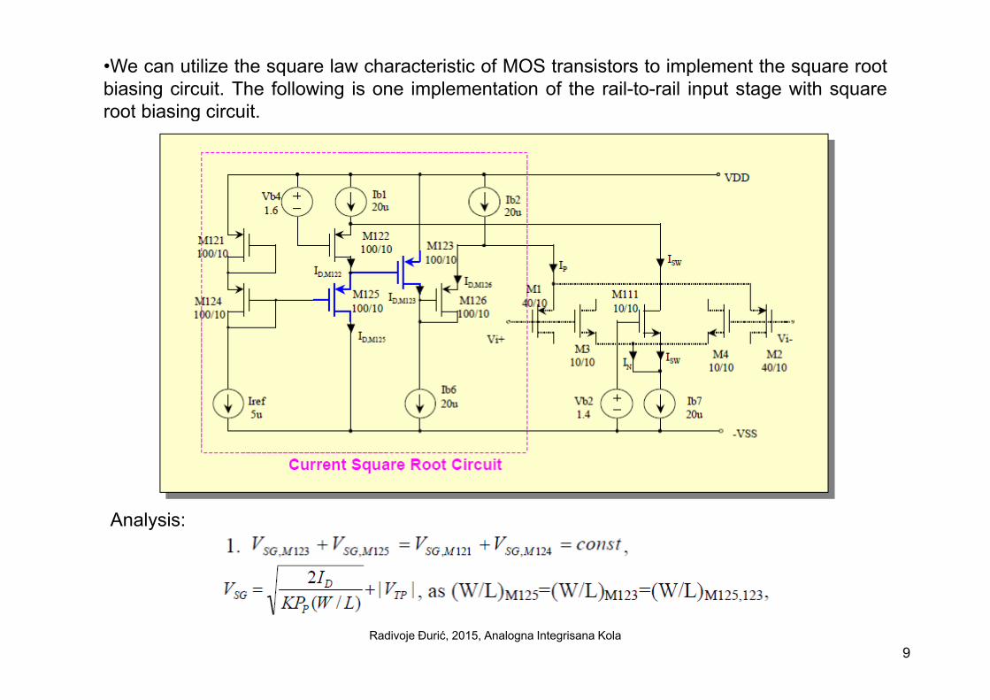
•We can utilize the square law characteristic of MOS transistors to implement the square rootbiasing circuit. The following is one implementation of the rail-to-rail input stage with squareroot biasing circuitroot biasing circuit.
Analysis:
Radivoje Đurić, 2015, Analogna Integrisana Kola9
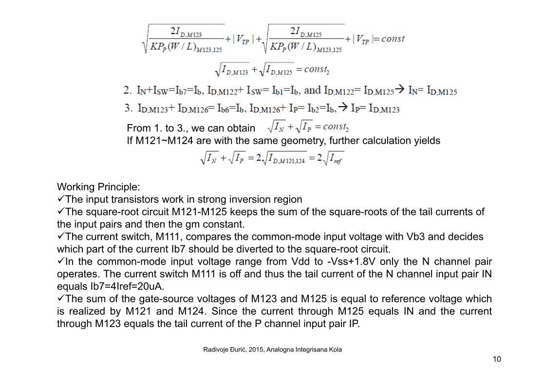
From 1. to 3., we can obtainIf M121~M124 are with the same geometry, further calculation yields
Working Principle:The input transistors work in strong inversion region The square-root circuit M121-M125 keeps the sum of the square-roots of the tail currents of the input pairs and then the gm constant. The current switch M111 compares the common mode input voltage with Vb3 and decidesThe current switch, M111, compares the common-mode input voltage with Vb3 and decides which part of the current Ib7 should be diverted to the square-root circuit. In the common-mode input voltage range from Vdd to -Vss+1.8V only the N channel pairoperates. The current switch M111 is off and thus the tail current of the N channel input pair INequals Ib7=4Iref=20uA.The sum of the gate-source voltages of M123 and M125 is equal to reference voltage whichis realized by M121 and M124. Since the current through M125 equals IN and the currentthrough M123 equals the tail current of the P channel input pair IP
Radivoje Đurić, 2015, Analogna Integrisana Kola10
through M123 equals the tail current of the P channel input pair IP.
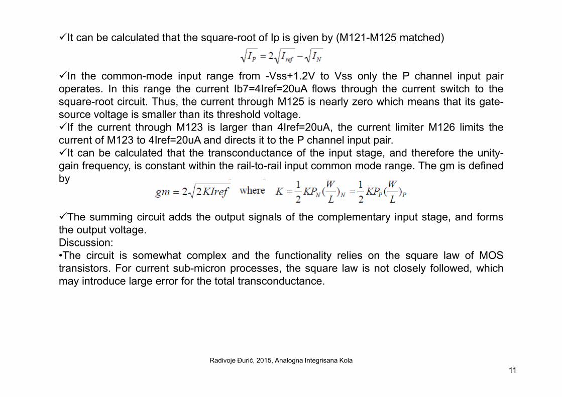
It can be calculated that the square-root of Ip is given by (M121-M125 matched)
In the common-mode input range from -Vss+1.2V to Vss only the P channel input pairoperates. In this range the current Ib7=4Iref=20uA flows through the current switch to thesquare-root circuit. Thus, the current through M125 is nearly zero which means that its gate-source voltage is smaller than its threshold voltage.If the current through M123 is larger than 4Iref=20uA, the current limiter M126 limits thecurrent of M123 to 4Iref=20uA and directs it to the P channel input pair.It can be calculated that the transconductance of the input stage and therefore the unity-It can be calculated that the transconductance of the input stage, and therefore the unity-gain frequency, is constant within the rail-to-rail input common mode range. The gm is definedby
The summing circuit adds the output signals of the complementary input stage, and formsthe output voltage.Discussion:Discussion: •The circuit is somewhat complex and the functionality relies on the square law of MOStransistors. For current sub-micron processes, the square law is not closely followed, whichmay introduce large error for the total transconductance.
Radivoje Đurić, 2015, Analogna Integrisana Kola11

3. Using current switches to change the tail current of input differential pairs
Basic ideaBasic idea•We know that, by first order approximation, for a MOS transistor working in strong inversionand saturation region, square law applies, that is
•Suppose for the N and P input pairs,
and the tail currents of N and P pairs are equal, with the value of Itail•When the input common mode voltage is in the mid-range, both of N and P pairs are
d ti th t t l t d t iconducting, so the total transconductance is
•When the input common mode voltage is close to Vdd, the N pair operates. And when it isp g , p pclose to the -Vss, the P pair operates. In both cases, the total transconductance is only half ofthat when both of N and P pairs operate.
•We can increase the tail current to 4 times of its original value to have the sametransconductance as that when both of N and P pairs operate.
Radivoje Đurić, 2015, Analogna Integrisana Kola12
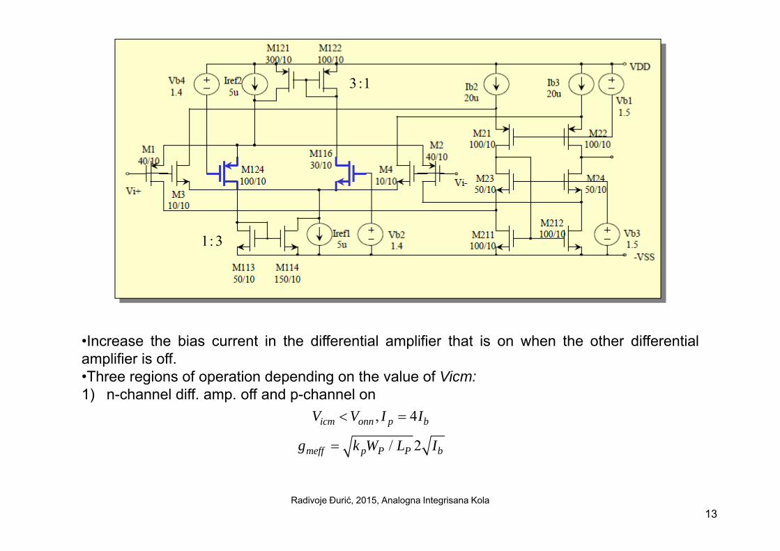
3:13 :1
1:3
Increase the bias c rrent in the differential amplifier that is on hen the other differential•Increase the bias current in the differential amplifier that is on when the other differentialamplifier is off.•Three regions of operation depending on the value of Vicm:1) n-channel diff. amp. off and p-channel on) p p
, 4icm onn p bV V I I
/ 2meff p P P bg k W L I
Radivoje Đurić, 2015, Analogna Integrisana Kola13
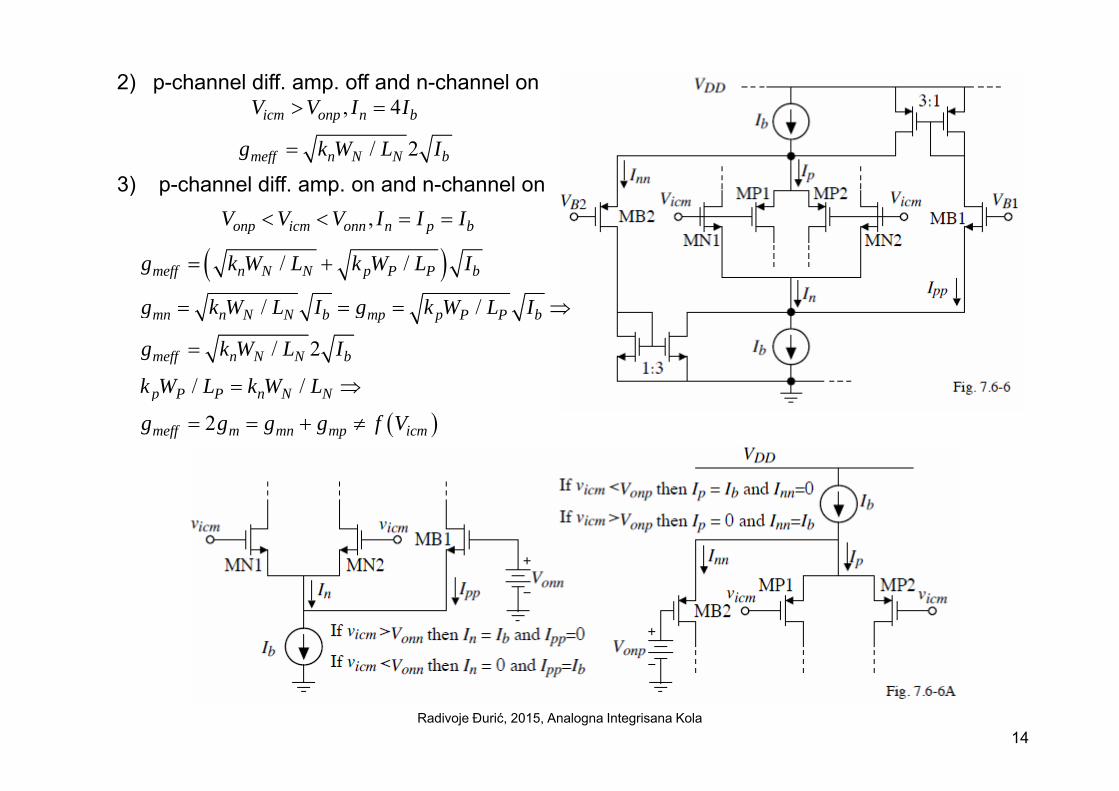
2) p-channel diff. amp. off and n-channel on, 4icm onp n bV V I I
3) p-channel diff. amp. on and n-channel on/ 2meff n N N bg k W L I
V V V I I I ,onp icm onn n p bV V V I I I
/ /meff n N N p P P bg k W L k W L I
/ /g k W L I g k W L I
/ /p P P n N Nk W L k W L
/ /
/ 2
mn n N N b mp p P P b
meff n N N b
g k W L I g k W L I
g k W L I
2p P P n N N
meff m mn mp icmg g g g f V
Radivoje Đurić, 2015, Analogna Integrisana Kola14
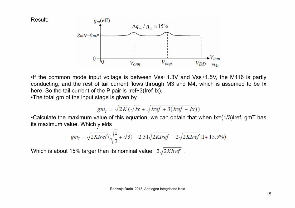
Result:/ 15%m mg g
•If the common mode input voltage is between Vss+1.3V and Vss+1.5V, the M116 is partlyconducting, and the rest of tail current flows through M3 and M4, which is assumed to be Ixhere. So the tail current of the P pair is Iref+3(Iref-Ix).•The total gm of the input stage is given by
•Calculate the maximum value of this equation, we can obtain that when Ix=(1/3)Iref, gmT hasits maximum value. Which yields
Which is about 15% larger than its nominal valueWhich is about 15% larger than its nominal value
Radivoje Đurić, 2015, Analogna Integrisana Kola15
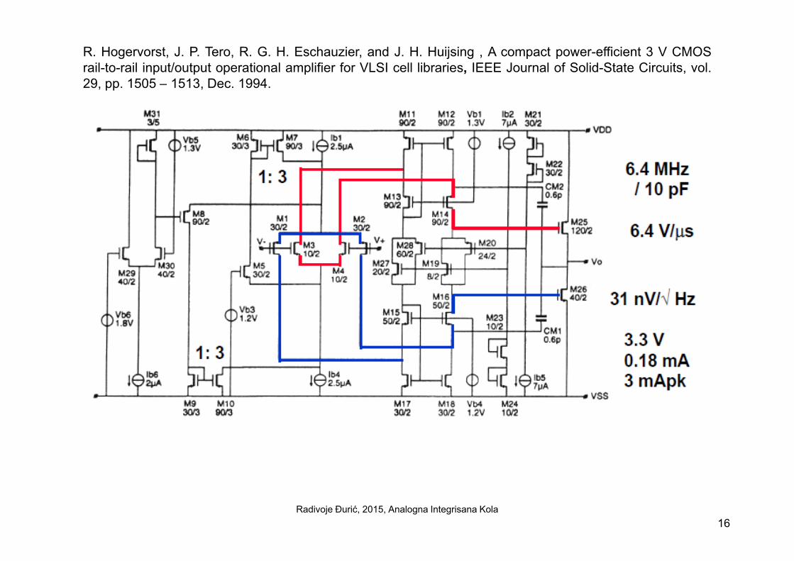
R. Hogervorst, J. P. Tero, R. G. H. Eschauzier, and J. H. Huijsing , A compact power-efficient 3 V CMOSrail-to-rail input/output operational amplifier for VLSI cell libraries, IEEE Journal of Solid-State Circuits, vol.29, pp. 1505 – 1513, Dec. 1994., pp ,
Radivoje Đurić, 2015, Analogna Integrisana Kola16

4. Using Maximum/Minimum selection circuitThe basic idea:The basic idea:•From previous analysis, we know that, when the common mode voltage drives the tail currenttransistor out of saturation region, the tail current of a differential pair decreases dramaticallywith the common mode voltage.Th diff ti l i hi h it i N i P i ith th l t h ld b ki•The differential pair, whichever it is N pair or P pair, with the larger current should be working
properly. We just try to choose the pair with larger working current, and discard the output ofanother pair.
Radivoje Đurić, 2015, Analogna Integrisana Kola17
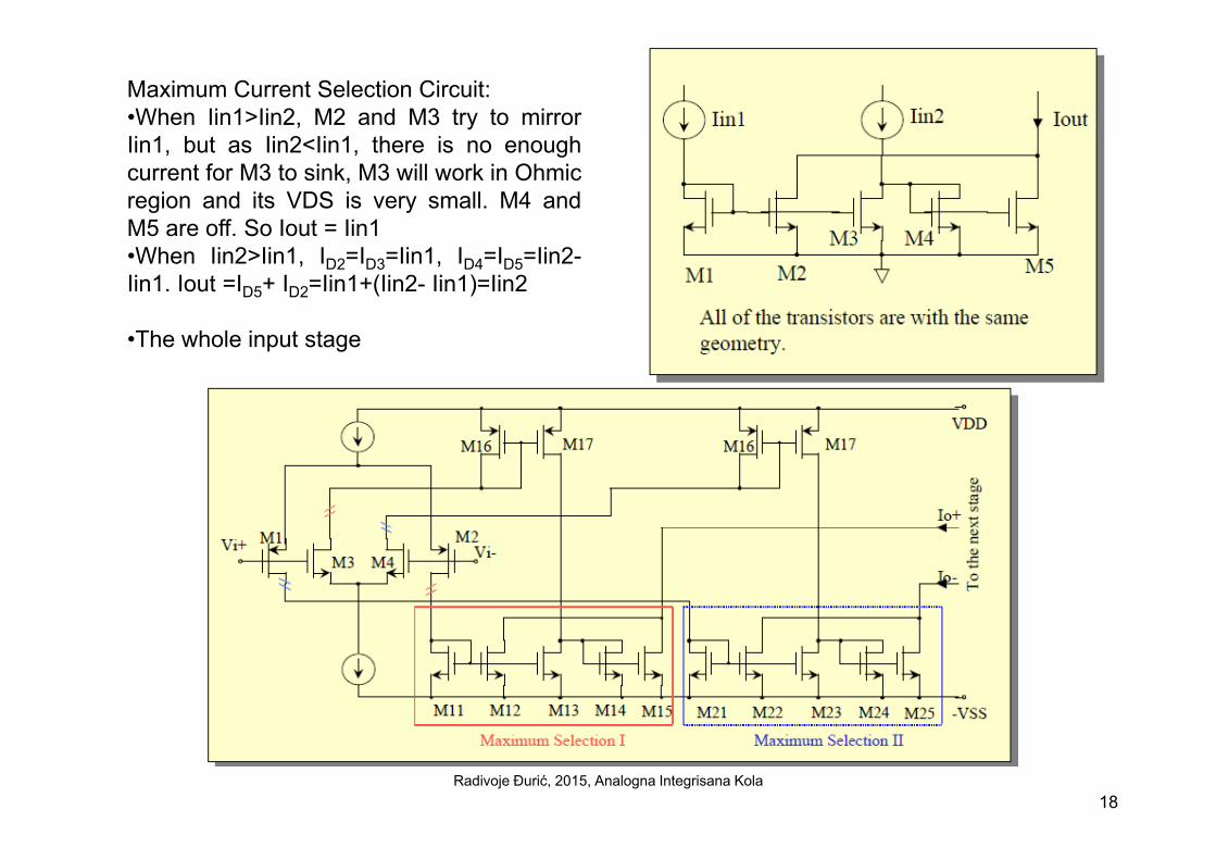
Maximum Current Selection Circuit:•When Iin1>Iin2, M2 and M3 try to mirrorIi 1 b t Ii 2 Ii 1 th i hIin1, but as Iin2<Iin1, there is no enoughcurrent for M3 to sink, M3 will work in Ohmicregion and its VDS is very small. M4 andM5 are off. So Iout = Iin1M5 are off. So Iout Iin1•When Iin2>Iin1, ID2=ID3=Iin1, ID4=ID5=Iin2-Iin1. Iout =ID5+ ID2=Iin1+(Iin2- Iin1)=Iin2
Th h l i t t•The whole input stage
Radivoje Đurić, 2015, Analogna Integrisana Kola18
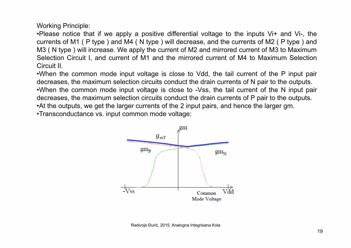
Working Principle:•Please notice that if we apply a positive differential voltage to the inputs Vi+ and Vi-, the
t f M1 ( P t ) d M4 ( N t ) ill d d th t f M2 ( P t ) dcurrents of M1 ( P type ) and M4 ( N type ) will decrease, and the currents of M2 ( P type ) andM3 ( N type ) will increase. We apply the current of M2 and mirrored current of M3 to MaximumSelection Circuit I, and current of M1 and the mirrored current of M4 to Maximum SelectionCircuit II.Circuit II.•When the common mode input voltage is close to Vdd, the tail current of the P input pairdecreases, the maximum selection circuits conduct the drain currents of N pair to the outputs.•When the common mode input voltage is close to -Vss, the tail current of the N input paird th i l ti i it d t th d i t f P i t th t tdecreases, the maximum selection circuits conduct the drain currents of P pair to the outputs.•At the outputs, we get the larger currents of the 2 input pairs, and hence the larger gm.•Transconductance vs. input common mode voltage:
mTg
Radivoje Đurić, 2015, Analogna Integrisana Kola19
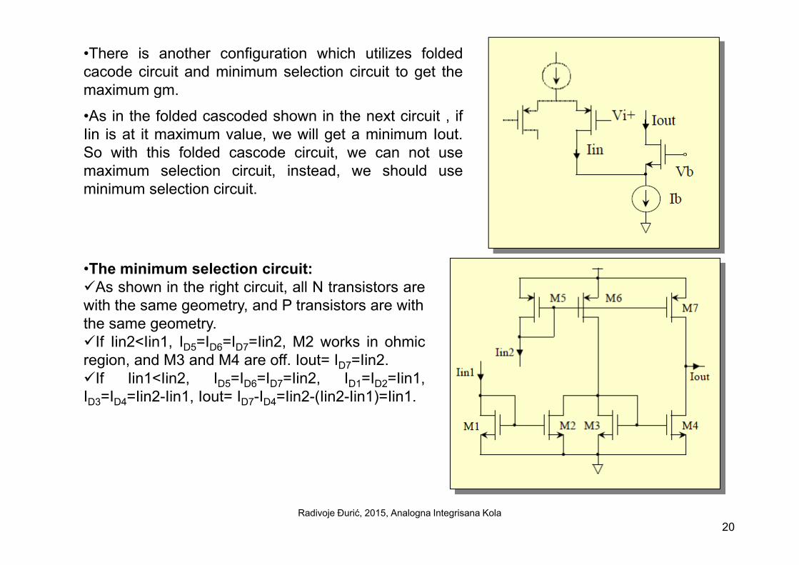
•There is another configuration which utilizes foldedcacode circuit and minimum selection circuit to get themaximum gmmaximum gm.
•As in the folded cascoded shown in the next circuit , ifIin is at it maximum value, we will get a minimum Iout.So with this folded cascode circuit we can not useSo with this folded cascode circuit, we can not usemaximum selection circuit, instead, we should useminimum selection circuit.
•The minimum selection circuit:A h i th i ht i it ll N t i tAs shown in the right circuit, all N transistors arewith the same geometry, and P transistors are withthe same geometry.If Iin2<Iin1, ID5=ID6=ID7=Iin2, M2 works in ohmicIf Iin2 Iin1, ID5 ID6 ID7 Iin2, M2 works in ohmicregion, and M3 and M4 are off. Iout= ID7=Iin2.If Iin1<Iin2, ID5=ID6=ID7=Iin2, ID1=ID2=Iin1,ID3=ID4=Iin2-Iin1, Iout= ID7-ID4=Iin2-(Iin2-Iin1)=Iin1.
Radivoje Đurić, 2015, Analogna Integrisana Kola20
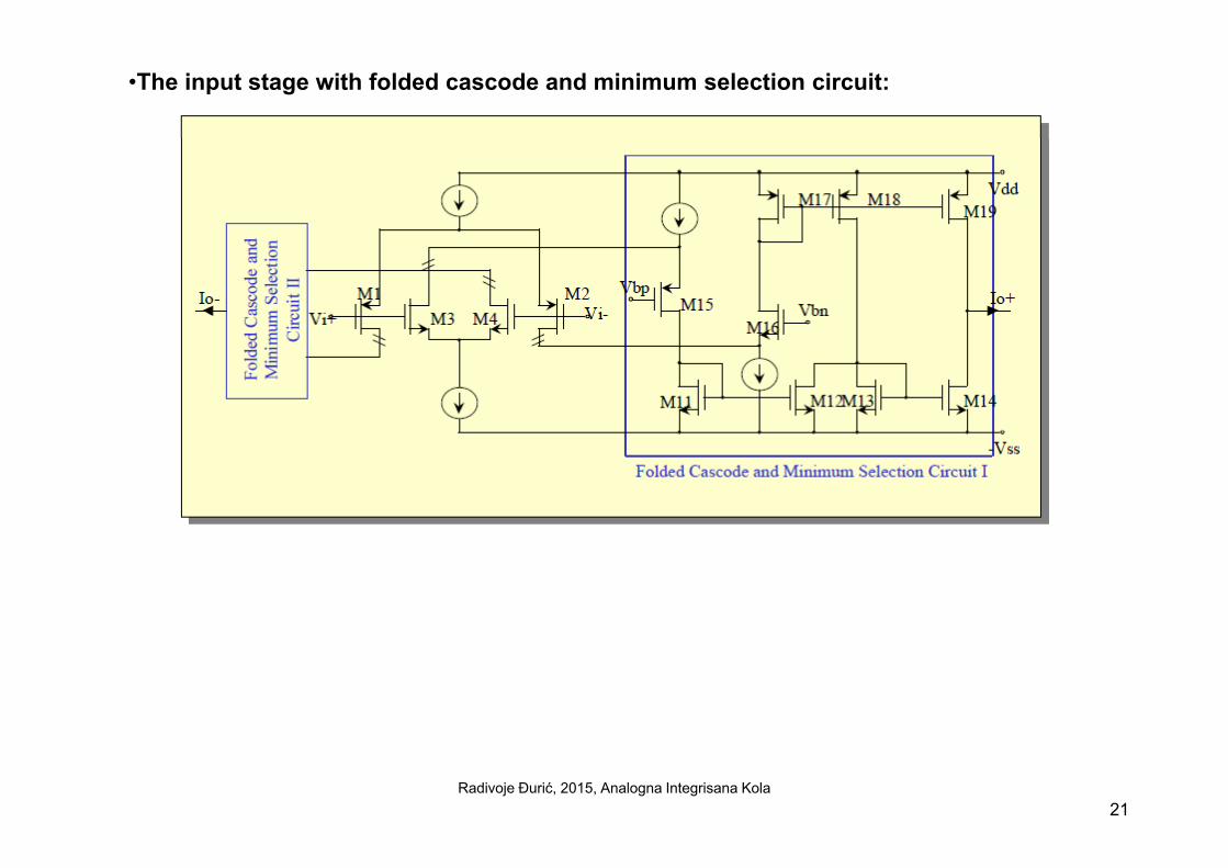
•The input stage with folded cascode and minimum selection circuit:
Radivoje Đurić, 2015, Analogna Integrisana Kola21