Embed Size (px)
Citation preview

4
Amorphous silicon waveguides formicrophotonics
Amorphous silicon a-Si was made by ion irradiation of crystalline silicon with 1�10��
Xe ions cm�� at 77 K in the 1–4 MeV energy range. Thermal relaxation of the amor-phous network at 500 ÆC for 1 hr leads to an amorphous layer with a refractive index of� = 3.73, significantly higher than that of crystalline silicon (� = 3.45 at � = 1.55 �m).a-Si can thus serve as a waveguide core in Si based optical waveguides. Channel wave-guides were made by anisotropic etching of a 1.5 �m silicon-on-insulator structure thatwas partly amorphized. Transmission measurements of these waveguides as function ofthe amorphous silicon length show that the a-Si part of the waveguides exhibit a modalpropagation loss of 70 cm�� (0.03 dB �m��) and a bulk propagation loss of 115 cm��
(0.05 dB �m��). Losses due to sidewall roughness are estimated, and are negligible com-pared to the modal loss. we conclude that a-Si waveguides are ideal for use in Si-basedmicrophotonics applications on a �100 �m length scale.

46 CHAPTER 4
4.1 Introduction
Silicon is the most widely used semiconductor material in today’s electronic devices, be-cause of its excellent electronic properties. Single crystalline Si of high quality is availableand the processing and microfabrication of Si are well known. Since silicon is transpar-ent in the near infrared, Si is also an ideal optical material. Si-based waveguides mayserve as optical interconnects on Si integrated circuits, or to distribute optical clock sig-nals on a microprocessor. In such cases, using Si provides the advantage of integrationwith existing electronic circuits. So far optical waveguide technology in silicon is notwell developed. Fabrication of waveguides in Si requires a core with a higher refractiveindex than that of crystalline Si (c-Si).
Amorphous Si (a-Si) is an interesting candidate as a core material. While the densityof pure a-Si is 1.8% lower than that of c-Si [72], the refractive index of pure a-Si, atnear-infrared wavelengths, is higher than that of c-Si [60, 73–75]. Amorphous siliconcan thus be used as a waveguide core material on crystalline Si. As pure a-Si contains alarge density of point defects and dangling bonds, the optical absorption at near-infraredwavelengths can be substantial. These point defects can be passivated to some extent byincorporation of hydrogen. In fact, hydrogenated a-Si made by deposition shows excellentelectrical quality, and relatively low optical absorption [76].
Amorphous silicon has already received a lot of interest both from a fundamentalpoint of view and because of its possible use in solar cells and optoelectronic devices.Hydrogenated a-Si films can be deposited using a number of different techniques, includ-ing plasma enhanced chemical vapor deposition (CVD), RF sputtering and hot-filamentCVD. The hydrogen content, void density, structural properties as well as optical andelectronic properties have been studied intensively and depend critically on the exact pro-cessing conditions. In contrast, a-Si made by ion irradiation of crystalline silicon hasreproducible properties that are insensitive to the preparation details, while voids seem tobe absent in this material [77]. Heat treatment of pure a-Si made by ion irradiation inducesstructural relaxation [78] and reduces the defect density, which leads to an improvementin the optical and electronic properties. Overall, it seems that hydrogenated a-Si has bettertransparency in the near-infrared than pure a-Si. However, pure a-Si can be made moreeasily in a Si processing sequence, as it requires a single ion implantation step. Further-more, pure a-Si has larger thermal stability then hydrogenated a-Si. Given these pro’s andcon’s of pure a-Si, it seems interesting to study its applicability in microphotonic inte-grated circuits. In this chapter we study the properties of amorphous silicon waveguidesmade using silicon-on-insulator (SOI) substrates and discuss the feasibility of a-Si wave-guides for silicon microphotonic channel waveguides and optical interconnects, and as aguiding layer in two-dimensional photonic crystals.
4.2 Properties of amorphous silicon
To study the amorphization and structural relaxation of a-Si, (100) orienteded c-Si sam-ples were mounted on a copper block that was kept at liquid nitrogen temperature. Sam-ples were irradiated with 1�10�� Xe ions cm�� in the 1–4 MeV energy range to formamorphous layers of different thickness. All irradiations were done with the ion beam in-cident under an angle of 7Æ with the surface normal to avoid ion channeling effects along
AMORPHOUS SILICON WAVEGUIDES FOR MICROPHOTONICS 47
Figure 4.1: RBS channeling spectra of amorphous silicon made by ion irradiation of crys-talline Si with 1.0�10�� Xe ions cm��. The Xe ion energy was 1 MeV. Spectra are shownfor the as implanted sample and for a sample annealed for 1 hr at 500 ÆC. For comparisona channeling spectrum of crystalline Si and a random Si spectrum are shown as well. Thesurface channel of Xe is indicated in the figure and the Gaussian distribution of Xe ions isclearly visible.
the (100) crystal direction. After irradiation the amorphous silicon was heat treated at500 ÆC for 1 hr in a vacuum tube furnace (base pressure �10�� mbar). The amorphouslayer thickness was measured by Rutherford backscattering spectrometry (RBS) channel-ing measurements using 2 MeV He� ions at a scattering angle of 165Æ. Variable anglespectroscopic ellipsometry in the 300–1700 nm wavelength was used to determine therefractive index of a-Si and to obtain independent information on the amorphous layerthickness.
The RBS channeling measurements for 1 MeV Xe irradiation are shown in Fig. 4.1.The data for ion irradiated samples are compared to channeling and random spectra ofunirradiated crystalline Si. As can be seen the Si signal follows the random height start-ing from the Si surface channel around channel 280, up to a certain depth in the sample forboth the as-implanted and the sample annealed at 500 ÆC for 1 hr. Annealing leads to theremoval of point defects and amorphous pockets in the c-Si near the a-Si/c-Si interface,which sharpens the interface. In addition, solid phase epitaxial crystallization takes placeat a growth rate of 0.083 A/s at 500 ÆC [79, 80] leading to a shift of the interface. Thisexplains the difference in channeling spectra between the as-implanted and annealed sam-ples. The Gaussian shaped profile around channel 390 is due to the implanted Xe ions.The peak of the implanted Xe distribution is roughly at the center of the a-Si thickness,and the Xe peak concentration is�0.08 at.%. From similar channeling measurements and

48 CHAPTER 4
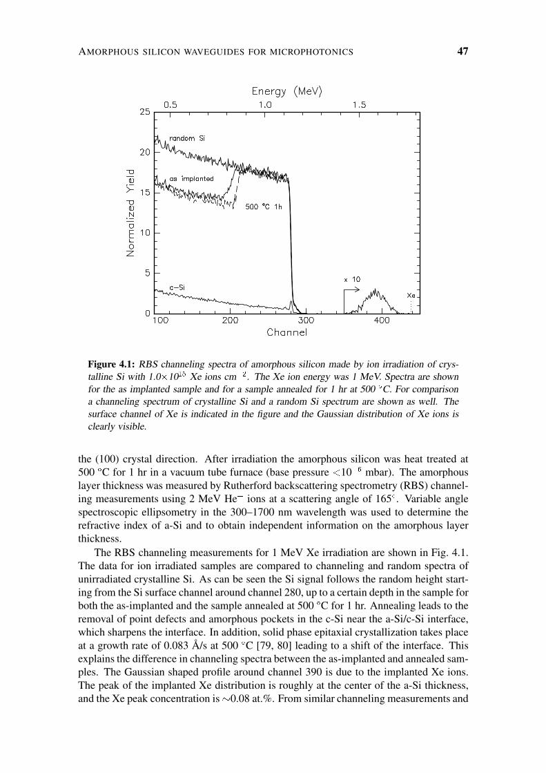
Figure 4.2: Real (n) and imaginary (k) part of the index of refraction for relaxed amorphoussilicon (drawn line) as function of wavelength, obtained from spectroscopic ellipsometrymeasurements. The index is compared to literature values for crystalline silicon (dashedlines) [81]. In the near-infrared part of the spectrum (� � 1100 nm) the refractive indexof amorphous is typically 0.3 higher than that of crystalline silicon, while the absorption issmall.
annealing studies we conclude that all samples irradiated with 1�10�� Xe ions cm�� inthe energy range 1–4 MeV, became amorphous up to the surface. The amorphous siliconthickness after annealing ranged from 0.6 �m for 1 MeV irradiation to 2.0 �m for 4 MeVirradiation.
Figure 4.2 shows the measured complex refractive index of amorphous silicon, madeby 1 MeV Xe irradiation, after thermal relaxation (drawn line) compared to literaturevalues for crystalline silicon (dashed line). After relaxation the ellipsometry data forwavelengths longer than 1.2 �m can be described with a lossless layer with a refractiveindex�0.3 higher than that of crystalline silicon. To obtain the layer thickness accuratelythe ellipsometry data was first fitted to a model assuming a transparent layer in the range� � 1200 nm�. The refractive index was then obtained for the entire wavelength range bypoint by point fitting of the complex refractive index, while keeping the layer thicknessfixed. By comparing data for samples made using different Xe ion energies it was foundthat the optical properties are independent of layer thickness. Also, samples annealed for2 hrs at 500 ÆC or for 1 hr at 550 ÆC gave the same results. The density of pure amorphoussilicon is lower than that of crystalline silicon [72] and thus a density difference cannot ex-plain the higher refractive index. Hence the high refractive index at infrared wavelengths
�To fit the ellipsometry data correctly, a 2.41 nm thick native oxide layer on top of the amorphous siliconwas used in the model.

AMORPHOUS SILICON WAVEGUIDES FOR MICROPHOTONICS 49
must be attributed to a difference in the electronic bandstructure. Such a difference isapparent from the data near the direct band-to-band transitions in the visible part of thespectrum as observed in Fig. 4.2. Ellipsometry as performed here is not sensitive to verysmall optical absorption. Given the experimental error on the ellipsometry data, an upperlimit of the loss coefficient of amorphous silicon at 1.5 �m is found: 100 cm��.
4.3 Amorphous silicon waveguides
To further investigate the optical losses of a-Si, commercially available silicon-on-insula-tor (SOI) substrates with a 1.5 �m thick (100) oriented p-type (14–22 �cm) Si layer on a3.0 �m thick SiO� layer grown by wet thermal oxidation were ion irradiated with 1�10��
2 MeV Xe ions cm�� at T = 77 K. The irradiation, followed by thermal relaxation at500 ÆC for 2 hrs leads to the formation of a �1.2 �m thick amorphous silicon layer.During irradiation part of the SOI substrate was masked leading to a triangularly shapedamorphous silicon surface layer on the substrate (see inset in Fig. 4.4).
After irradiation, a series of 10 �m wide waveguides at a 50 �m repeat distance weredefined using electron-beam lithography and deep anisotropic etching. Mask patternswere defined in a resist double layer consisting of a 400 nm thick hard baked photoresistlayer (HPR 504), with a 80 nm thick silicon containing negative tone electron-beam resist(SNR) on top. After electron-beam exposure (100 kV, 150 �C cm��) the pattern wasdeveloped for 20 s in xylene and rinsed for 30 s in iso-propyl-alcohol. The pattern wasthen anisotropically transferred in the bottom photoresist layer by low pressure O� reactiveion etching at room temperature (p = 0.3 Pa, 0.07 W cm�� RF power density, -180 V DC-bias). Before etching the underlying Si, a dip in hydrofluoric acid (4%) was used toremove the thin native oxide. The pattern was then transferred in the silicon by electron-cyclotron resonance (ECR) driven plasma etching using a low pressure (0.1 Pa) SF�/O�
gas mixture (5.6:1.0) at -95 ÆC. A microwave power of 400 W was used, combinedwith a -15 V DC-bias, resulting in an etch rate of �300 nm min�� and anisotropic etchprofiles [51]. All patterning processes were controlled in situ by laser interferometry.The Si was etched back till the etching stopped at the underlying oxide layer, resulting in1.5 �m high Si profiles�.
Fig. 4.3 shows bright field cross sectional transmission electron microscopy (TEM)images of the waveguides taken using 300 kV electrons. Cross sections were first sawcut to 0.5-1 mm thickness, then thinned to 15 �m thickness by mechanical grinding andpolishing, and finally ion milled with 5 kV Ar ions to electron transparency. Figure 4.3a)shows the waveguide structure of the amorphous Si waveguide. The cross section showsa 1.06 �m thick amorphous Si region on top of a 0.45 �m crystalline Si layer on a 3.0 �mthick SiO� layer. As can be seen, the anisotropic ECR etching process has proceededcontinuously through the a-Si/c-Si interface and leads to a similar side-wall angle for bothmaterials. Figures 4.3b) and 4.3c) zoom in on the sidewalls of the a-Si waveguide and c-Siwaveguide respectively. They show small sidewall roughness, as will be discussed furtheron.
�The a-Si layer has a 30% lower etch rate than the (100)-oriented c-Si. The etching process was con-trolled on the a-Si part of the sample, thus slightly overetching the c-Si part.

50 CHAPTER 4
b) c)
a)
1 m�
500 nm 500 nm
a-Si
c-Si
SiO2
Figure 4.3: Cross section TEM images of amorphous silicon channel waveguides on c-Si onSiO�. (a) cross section of the amorphized crystalline region, (b) sidewall of a-Si guide and(c) sidewall of c-Si guide. The thickness of the cross-sections is 610 nm (b) and 310 nm (c).
4.4 Results and discussion
For optical transmission measurements, waveguide samples were saw-cut to �7 mmlength. The end faces were mechanically polished in order to attain an optimal light cou-pling into the waveguides. Transmission measurements at � = 1.49 �m were performedby coupling an InGaAsP laser diode into the waveguides using a tapered optical fiber.6% of the input power was split off to monitor the input power from the laser. The fiberalignment was controlled using piezo electric actuators. Mode images were obtained byimaging the light from the output facet on an infrared camera using a 10� microscopeobjective. For transmission measurements, the output mode was collected by a Ge diodedetector and was compared to the input power monitored simultaneously on an identicalGe diode detector.
Figure 4.4 shows the measured transmission (open circles) for a series of 70 wave-guides. A schematic of the measurement setup with the amorphous and crystalline partsof the waveguides indicated is shown in the inset. The first �12 waveguides are crys-talline along their full length. By moving the input fiber along the horizontal direction onthe sample, waveguides with an amorphous section of increasing length are probed. Ascan be seen, the measured transmission drops exponentially with increasing a-Si length.From the angle of the triangular amorphous region it is known that the amorphous siliconlength increases by 25 �m per guide. This information was used to convert the horizontalscale to a length scale (top axis). The best fit to the data (dashed line in Fig. 4.4) resultsin an extinction coefficient of � = 70 cm�� (0.03 dB �m��). This is consistent with theupper limit of 100 cm�� derived from ellipsometry in section 4.2.
The transmission in Fig. 4.4 is measured relative to the input power in the taperedfiber and thus contains both the coupling loss and collection efficiency in our setup. The

AMORPHOUS SILICON WAVEGUIDES FOR MICROPHOTONICS 51
Figure 4.4: Measured transmission (����) of c-Si waveguides with a short a-Si section asfunction of guide number (bottom axis) and a-Si length (top axis). The collection efficiencyis estimated (see text) and is indicated on the left axis and is used as the 0 dB point ofthe waveguide loss indicated on the right axis. Measurements are shown after structuralrelaxation at 500 Æc for 2 hrs (Æ) and after additional annealing at 500 ÆC for 1 hr in a forminggas (10% H� / 90% N�) atmosphere(�). A schematic representation of the sample geometryis shown in the inset.
collection efficiency was measured to be 4% by directly collecting the laser light fromthe tip of the tapered fiber without a waveguide. This value is indicated by the arrowin Fig. 4.4. The right axis in Fig. 4.4 shows waveguide loss in dB, corrected for thiscollection efficiency. The combined transmission and coupling losses through the 7 mmlong crystalline waveguides (i. e. without a-Si) is less than 9 dB, which corresponds to� � 3 cm��. This is insignificant compared to the value of 70 cm�� measured for the a-Siwaveguides.
In the remainder of this chapter we will discuss the nature of the optical loss of a-Siwaveguides. Several loss mechanisms should be considered, including coupling losses,scattering losses due to sidewall roughness, and intrinsic material losses. Free carrierabsorption can in our case be neglected since the experiments were carried out on lightlydoped Si�.
Coupling loss occurs when coupling from the tapered input fiber to the waveguideand also when the mode crosses the junction between the c-Si and a-Si section of thewaveguides as they have different optical mode sizes. Both types of coupling loss can beestimated from the mode overlap that can be calculated based on measured mode profiles.The measured output modes of the waveguides and the tapered fiber are both described
�The free carrier concentration in the p-type Si waveguides (14–22 �cm) is �1.0�10�� cm��. Usingan absorption cross section of 0.64�10��� cm� [82], this leads to a loss coefficient � �6�10��, so thatfree carrier absorption can be safely neglected.

52 CHAPTER 4
satisfactorily by Gaussian shaped mode profiles. Assuming optimum alignment fromfiber to waveguide, a lower limit of the coupling loss of 0.45 dB can be estimated. Theloss occurring at the transition from the c-Si to a-Si part of the waveguide is calculatedusing the waveguide modes obtained from a finite element simulation. The loss due tomode mismatch is estimated to be 0.25 dB (94% transmission). Note that the couplinglosses lead to a vertical shift of the data in Fig. 4.4 and do not affect the exponential decayobserved.
To investigate scattering losses due to sidewall roughness, TEM images of the wave-guide cross section (see Fig. 4.3b) and Fig. 4.3c)) and scanning electron microscopy(SEM) images (not shown) taken from the top and along the propagation direction wereused to measure roughness of both the c-Si and a-Si waveguide sidewalls. A sidewallroughness (�) of �5 nm for c-Si and �10 nm for a-Si is derived. These values are con-firmed by the SEM images (resolution of �5 nm.) taken from the top. As can be seenin Fig. 4.3b) the roughness at the a-Si to c-Si interface is small, and is expected to be ofatomic scale [83]. To calculate the scattering losses due to surface roughness, we use anexpression derived by Tien [84] based on the Rayleigh criterion:
�� � ���
������
�
��
���
���
� ����� ��� �
��� (4.1)
where �� is the variance of the surface roughness, �� is the wavelength in the guidinglayer, � is the thickness of the guiding layer. is the mode angle of the mode propagatingin the waveguide and ��� and �� are the penetration depths of the mode into the cladding.Using the calculated propagation constant of the waveguides as obtained from a finiteelement simulation and the measured values for �, the scattering loss can be estimated tobe 0.1 cm�� (0.4 dB cm��) for the c-Si guide and 0.4 cm�� (1.6 dB cm��) for the a-Siwaveguide. These values are much lower than the loss of 70 cm�� found from Fig. 4.4. Infact, a sidewall roughness of � = �200 nm is needed to obtain a loss figure of 70 cm��,which would strongly disagree with the TEM data of Fig. 4.3. Therefore we concludethat the measured loss of the a-Si waveguide is mainly due to intrinsic absorption in theamorphous silicon itself. To convert the modal loss of 70 cm�� to the intrinsic absorptioncoefficient of amorphous silicon, the confinement factor of the waveguide mode should betaken into account. Both from the experimentally measured mode and the finite elementcalculation a typical confinement factor of 60% is estimated. The absorption coefficientof amorphous silicon at 1.5 �m is thus estimated to be 115 cm�� (0.05 dB �m��).
It is known that hydrogen can passivate point defects in a-Si and could thus reduce theabsorption observed at 1.5 �m. To study this, the waveguide sample as described abovewas annealed in a forming gas atmosphere (10% H� / 90% N�) at 500 ÆC for 1 hr. Givena typical diffusion constant of H� in silicon, hydrogen could diffuse�30 �m into the a-Sinetwork and passivate defects inside the a-Si. Other experiments indicate that under theseconditions concentrations of a few at.% atomic hydrogen can be incorporated in a-Si [85].The + symbols in Fig. 4.4 show the transmission measured after this hydrogen treatment.It cannot be distinguished from the transmission measured before annealing in hydrogen.Apparently it is not possible to passivate defects responsible for absorption losses in a-Simade by MeV ion-irradiation by the thermal treatment described above.
The optical loss in a-Si waveguides described in this chapter (0.05 dB �m��) makea-Si an ideal waveguide core material in Si microphotonic circuits. With typical dimen-sions well below 100 �m, intrinsic losses on the scale of such devices would be quite

AMORPHOUS SILICON WAVEGUIDES FOR MICROPHOTONICS 53
Figure 4.5: Example of a Si photonic crystal device with a 2 �m thick a-Si top section toconfine the light vertically. The device consist of an array of 205 nm diameter cylindrical Sirods placed on a square lattice with a lattice constant � = 570 nm. The rods are 5 �m long andhave a 2 �m thick a-Si top section to confine the light vertically. The remaining photoresist isclearly visible on top of the pillars. A row of rods is removed from the array to define a 90Æ
waveguide bend. Input and output channel waveguides to test the device are defined as well.The inset zooms in on the entrance of the photonic crystal waveguide and clearly shows theremoved row of rods together with the input waveguide.
tolerable. As the fabrication of a-Si using ion irradiation is fully compatible with Si mi-crofabrication and integrated circuit processing this enables the fabrication of waveguidesin Si, with the vertical confinement provided by the higher index a-Si. To keep the dimen-sions of these devices as small as possible and to obtain a high packing density requireswaveguides that can make very small bends. With the high refractive index of a-Si abending radius of order 1 �m may be achieved [86, 87]. Alternatively, 2-dimensional(2-D) photonic crystal structures have been proposed to achieve high transmission for 90Æ
bends with very small radius of curvature [11, 12]. In the remainder of this chapter wewill describe how a combination of a-Si waveguides and Si photonic crystal technologymay be used to achieve such a small bending radius for the important telecommunicationwavelength of 1.5 �m.
Figure 4.5 shows a SEM image of 2-D Si photonic crystal waveguide bend designedfor operation at 1.5 �m wavelength. The device consist of an array of 205 nm diametercylindrical Si rods placed on a square lattice with a lattice constant � = 570 nm. Therods are 5 �m long and have a 2 �m thick a-Si top section to confine the light in thevertical direction. Input and output channel waveguides to test the device are defined aswell. The inset zooms in on the entrance of the photonic crystal waveguide and clearlyshows the removed row of rods and the input waveguide. The mask pattern for this devicewas defined by electron-beam lithography and oxygen reactive ion etching following thesame processing as for the channel waveguides discussed earlier and described in detail

54 CHAPTER 4
in Chapter 3 . The Si etch process was more carefully tuned because of the smallerfeature sizes and higher aspect ratios involved. The photonic waveguide bend structuresare dry etched in an ECR plasma of SF�/O� (7.3:1) at a pressure of 0.1 Pa, a substratetemperature of -97 ÆC, a �wave power of 400 W and a DC bias of -12 V, resulting in anetch rate of about 150 nm min��. Details of the device fabrication procedure are publishedelsewhere [51].
The design of these devices is based on photonic bandstructure calculations of a squarelattice of (infinitely long) Si rods. The vertical confinement in the top a-Si section is basedon an effective index method as described in Chapter 2. The properties of a structurewith rods of finite length that have a top section of higher refractive index show similarbehavior as infinitely long cylinders if the top section is large enough [52]. To calculatethe detailed optical response and vertical confinement in devices like the one depicted inFig. 4.5 a three-dimensional calculation is needed.
The next challenge is to characterize the transmission characteristics of the bends.In this analysis, the main problem is the fact that the mm-long a-Si input and outputwaveguides suffer from high loss. This once again shows that in studies of microphotonicmaterials, the coupling to the outside macroscopic world is a matter of great importanceand concern. In future microphotonic integrated devices, such problems can be minimizedby integrating as many optical function as possible on a single optical chip.
4.5 Conclusions
We have fabricated amorphous silicon (a-Si) waveguides by combining MeV Xe ion irra-diation with anisotropic etching techniques. Transmission measurements on 10 �m widewaveguides with different a-Si length revealed a modal absorption coefficient of 70 cm��
(0.03 dB �m��) at a wavelength of 1.5 �m. Annealing of the waveguides in a hydrogenatmosphere did not improve the optical properties of the waveguides. The scattering lossof the waveguides due to sidewall roughness was calculated and found to be insignificantcompared to the total modal loss. Taking the confinement factor of 60% into account theintrinsic absorption coefficient of a-Si made by ion irradiation is found to be 115 cm��
(0.05 dB �m��). Since the processing of a-Si made by ion irradiation is compatible withstandard Si microfabrication and integrated circuit technology, a-Si can be used to verti-cally confine light in microphotonic devices with dimensions well below 100 �m. As anexample a 2-D photonic crystal device is presented in which the vertical confinement maybe achieved by index guiding in a 2 �m thick a-Si top section.