Embed Size (px)
Citation preview
University of Tennessee, Knoxville University of Tennessee, Knoxville
TRACE: Tennessee Research and Creative TRACE: Tennessee Research and Creative
Exchange Exchange
Masters Theses Graduate School
8-2016
An Application of the Universal Verification Methodology An Application of the Universal Verification Methodology
Rui Ma University of Tennessee, Knoxville, [email protected]
Follow this and additional works at: https://trace.tennessee.edu/utk_gradthes
Part of the Computer and Systems Architecture Commons
Recommended Citation Recommended Citation Ma, Rui, "An Application of the Universal Verification Methodology. " Master's Thesis, University of Tennessee, 2016. https://trace.tennessee.edu/utk_gradthes/4054
This Thesis is brought to you for free and open access by the Graduate School at TRACE: Tennessee Research and Creative Exchange. It has been accepted for inclusion in Masters Theses by an authorized administrator of TRACE: Tennessee Research and Creative Exchange. For more information, please contact [email protected].
To the Graduate Council:
I am submitting herewith a thesis written by Rui Ma entitled "An Application of the Universal
Verification Methodology." I have examined the final electronic copy of this thesis for form and
content and recommend that it be accepted in partial fulfillment of the requirements for the
degree of Master of Science, with a major in Computer Engineering.
Gregory D. Peterson, Major Professor
We have read this thesis and recommend its acceptance:
Syed Kamrul Islam, Garrett S. Rose
Accepted for the Council:
Carolyn R. Hodges
Vice Provost and Dean of the Graduate School
(Original signatures are on file with official student records.)
An Application of the Universal
Verification Methodology
A Thesis Presented for the
Master of Science
Degree
The University of Tennessee, Knoxville
Rui Ma
August 2016
c© by Rui Ma, 2016
All Rights Reserved.
ii
To my daughter, Shumin Jia.
iii
Abstract
The Universal Verification Methodology (UVM) package is an open-source Sys-
temVerilog library, which is used to set up a class-based hierarchical testbench.
UVM testbenches improve the reusability of Verilog testbenches. Direct Memory
Access (DMA) plays an important role in modern computer architecture. When
using DMA to transfer data between a host machine and field-programmable gate
array (FPGA) accelerator, a modularized DMA core on the FPGA frees the host side
Central Processing Unit(CPU) during the transfer, helps to save FPGA resources,
and enhances performance. Verifying the functionality of a DMA core is essential
before mapping it to the FPGA. In this thesis, we tested an open source DMA core
with UVM (Universal Verification Methodology). Bus agents and interface modules
are designed for input and output signals of the DMA Design Under Test (DUT). We
constructed a Register Level Abstraction (RLA) model to allow both front-door access
and back-door access to the register files in the DUT. We designed the sequences,
scoreboards, and tests with features to allow reuse. The overall testbench structure
is defined by a base-type test. Different tests then extend the base-type test and use
type overriding with the UVM configuration database to use different scoreboards and
sequences accordingly. With scoreboard and coverage groups, the testbench monitors
the correctness of the behavior of the DMA DUT, as well as the functional coverage
of all tests. We performed the simulations with the Questa simulator. Several bugs
in the open-source DMA core were found and corrected.
iv
Table of Contents
1 Introduction 1
1.1 Introduction to Verification and the UVM . . . . . . . . . . . . . . . 1
1.2 Introduction to DMA . . . . . . . . . . . . . . . . . . . . . . . . . . . 4
1.3 Goal of Research . . . . . . . . . . . . . . . . . . . . . . . . . . . . . 5
2 Background 8
2.1 Introduction . . . . . . . . . . . . . . . . . . . . . . . . . . . . . . . . 8
2.2 DMA Operations . . . . . . . . . . . . . . . . . . . . . . . . . . . . . 10
2.2.1 DMA Operations . . . . . . . . . . . . . . . . . . . . . . . . . 10
2.2.2 Other Functionality . . . . . . . . . . . . . . . . . . . . . . . . 13
2.2.3 Host and Device Memory Organization . . . . . . . . . . . . . 13
2.3 Conclusions . . . . . . . . . . . . . . . . . . . . . . . . . . . . . . . . 14
3 UVM Testbench Design 15
3.1 Overall Structures . . . . . . . . . . . . . . . . . . . . . . . . . . . . . 15
3.2 Agents . . . . . . . . . . . . . . . . . . . . . . . . . . . . . . . . . . . 17
3.3 Transactions . . . . . . . . . . . . . . . . . . . . . . . . . . . . . . . . 18
3.4 Register Level Abstraction . . . . . . . . . . . . . . . . . . . . . . . . 20
3.5 Sequences . . . . . . . . . . . . . . . . . . . . . . . . . . . . . . . . . 22
3.6 Coveragegroup . . . . . . . . . . . . . . . . . . . . . . . . . . . . . . 24
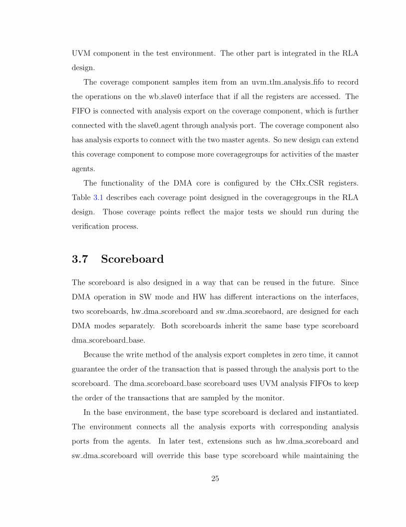
3.7 Scoreboard . . . . . . . . . . . . . . . . . . . . . . . . . . . . . . . . . 25
3.8 Tests . . . . . . . . . . . . . . . . . . . . . . . . . . . . . . . . . . . . 27
v
3.9 Conclusions . . . . . . . . . . . . . . . . . . . . . . . . . . . . . . . . 30
4 Simulations and Results 31
4.1 Test Cases Illustration . . . . . . . . . . . . . . . . . . . . . . . . . . 31
4.2 Simulation and Results . . . . . . . . . . . . . . . . . . . . . . . . . . 33
4.2.1 General . . . . . . . . . . . . . . . . . . . . . . . . . . . . . . 33
4.2.2 Simulation Results . . . . . . . . . . . . . . . . . . . . . . . . 34
4.2.3 Other Tests . . . . . . . . . . . . . . . . . . . . . . . . . . . . 40
4.2.4 Bugs and Debug . . . . . . . . . . . . . . . . . . . . . . . . . 42
4.2.5 Coverage Collection and Discussion . . . . . . . . . . . . . . . 44
4.3 Conclusions . . . . . . . . . . . . . . . . . . . . . . . . . . . . . . . . 44
5 Conclusions and Future Work 46
Bibliography 48
Appendix 51
A Script and Code 52
A.1 Simulation Script in Tcl . . . . . . . . . . . . . . . . . . . . . . . . . 52
A.2 Code Modifications . . . . . . . . . . . . . . . . . . . . . . . . . . . . 54
Vita 56
vi
List of Tables
2.1 DMA registers . . . . . . . . . . . . . . . . . . . . . . . . . . . . . . . 10
3.1 Coverage point for the CHx CSR reigsters. . . . . . . . . . . . . . . . 26
4.1 Channel CSR configuration for software mode DMA . . . . . . . . . . 32
4.2 DMA operation directions . . . . . . . . . . . . . . . . . . . . . . . . 33
4.3 Tests description . . . . . . . . . . . . . . . . . . . . . . . . . . . . . 34
vii
List of Figures
1.1 A typical Verilog testbench . . . . . . . . . . . . . . . . . . . . . . . . 2
1.2 Inheritance of UVM classes . . . . . . . . . . . . . . . . . . . . . . . 3
1.3 A typical UVM testbench . . . . . . . . . . . . . . . . . . . . . . . . 4
1.4 An application example with DMA module . . . . . . . . . . . . . . . 6
2.1 Interface groups of the DMA core . . . . . . . . . . . . . . . . . . . . 9
2.2 Block level diagram of the DMA controller . . . . . . . . . . . . . . . 11
2.3 Register layout of CHx SZ, CHx DESC, and CHx SWPTR . . . . . . 12
2.4 Layout of CHx CSR register . . . . . . . . . . . . . . . . . . . . . . . 12
3.1 Overall testbench structures . . . . . . . . . . . . . . . . . . . . . . . 16
3.2 Transactions . . . . . . . . . . . . . . . . . . . . . . . . . . . . . . . . 18
3.3 Top-level register block and map design . . . . . . . . . . . . . . . . . 20
3.4 Register Level Abstraction (RLA) . . . . . . . . . . . . . . . . . . . . 21
3.5 Inheritance of register sequence . . . . . . . . . . . . . . . . . . . . . 23
3.6 Inheritance of misc item sequence . . . . . . . . . . . . . . . . . . . . 23
3.7 Sequence order . . . . . . . . . . . . . . . . . . . . . . . . . . . . . . 24
3.8 Scoreboard for DMA in HW mode . . . . . . . . . . . . . . . . . . . 28
3.9 Scoreboard for DMA in SW mode . . . . . . . . . . . . . . . . . . . . 29
3.10 Inheritance of tests . . . . . . . . . . . . . . . . . . . . . . . . . . . . 30
4.1 Scenarios for tests . . . . . . . . . . . . . . . . . . . . . . . . . . . . . 35
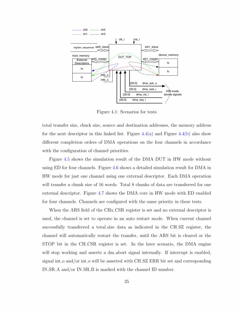
4.2 Simulation structure . . . . . . . . . . . . . . . . . . . . . . . . . . . 36
viii
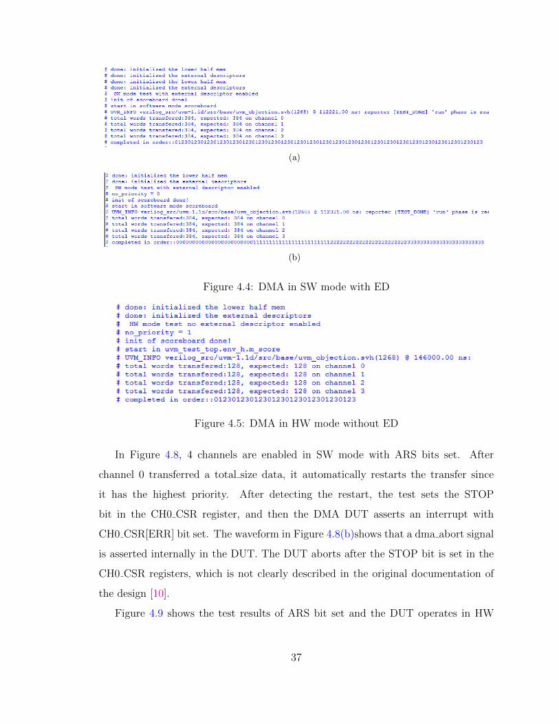
4.3 DMA in SW mode without ED . . . . . . . . . . . . . . . . . . . . . 36
4.4 DMA in SW mode with ED . . . . . . . . . . . . . . . . . . . . . . . 37
4.5 DMA in HW mode without ED . . . . . . . . . . . . . . . . . . . . . 37
4.6 One channel test in HW mode with ED . . . . . . . . . . . . . . . . . 38
4.7 DMA in HW mode with ED . . . . . . . . . . . . . . . . . . . . . . . 38
4.8 DMA in SW mode with ARS enabled . . . . . . . . . . . . . . . . . . 39
4.9 DMA in HW mode with ARS enabled . . . . . . . . . . . . . . . . . 39
4.10 Hardware restart enabled . . . . . . . . . . . . . . . . . . . . . . . . . 40
4.11 Forcing the next descriptor in HW mode . . . . . . . . . . . . . . . . 40
4.12 Peak-poke test . . . . . . . . . . . . . . . . . . . . . . . . . . . . . . . 41
4.13 HW DMA in back-to-back timing . . . . . . . . . . . . . . . . . . . . 41
4.14 HW DMA in dma req/dma ack timing . . . . . . . . . . . . . . . . . 42
4.15 Bug: de start not asserted after req i issued . . . . . . . . . . . . . . 42
4.16 Debug: de start asserted after req i is issued . . . . . . . . . . . . . . 42
4.17 Bug: the timing error of inta o and intb o in the design . . . . . . . . 43
4.18 Debug: the timing error of inta o and intb o simulation result . . . . 43
4.19 Suspicious completion orders . . . . . . . . . . . . . . . . . . . . . . . 44
4.20 Coveragegroup statistics . . . . . . . . . . . . . . . . . . . . . . . . . 45
ix
Chapter 1
Introduction
1.1 Introduction to Verification and the UVM
During the past decade, Verification plays an important role than ever in today’s
semiconductor industry. The demand for design engineers grew at a rate of less than
4%. Meanwhile, the number of verification engineers increased about 3.5x the number
of design engineers [18]. Before the Universal Verification Methodology (UVM) was
adopted by the academy and the industry, different projects each might have their
own verification process. Even for the same Design Under Test (DUT), different
groups may carry out different testbench designs. Without a unified verification
methodology, testbench design lacks of reusability, which holds back the productivity
of both design and verification groups.
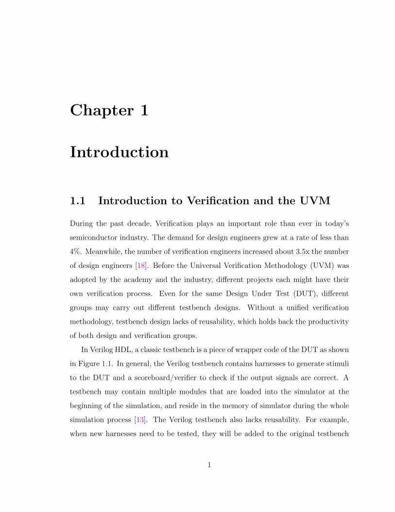
In Verilog HDL, a classic testbench is a piece of wrapper code of the DUT as shown
in Figure 1.1. In general, the Verilog testbench contains harnesses to generate stimuli
to the DUT and a scoreboard/verifier to check if the output signals are correct. A
testbench may contain multiple modules that are loaded into the simulator at the
beginning of the simulation, and reside in the memory of simulator during the whole
simulation process [13]. The Verilog testbench also lacks reusability. For example,
when new harnesses need to be tested, they will be added to the original testbench
1
DUT
testbench
harness
harness...
harness
verifier
Figure 1.1: A typical Verilog testbench.
and all of the harnesses in the testbench will be compiled and simulated again. If
setting up a new testbench with new harnesses, then copying and pasting code can
not be avoided, for example, to instantiate the DUT.
SystemVerilog language is an extended version of Verilog. It has several features
that make it more advantageous than Verilog especially in developing testbenches [11].
Specifically, it has Object-Oriented mechanisms to allow the testbench to be abstract.
It also has other features such as constraint and covergroups to make the testbench
more efficient.
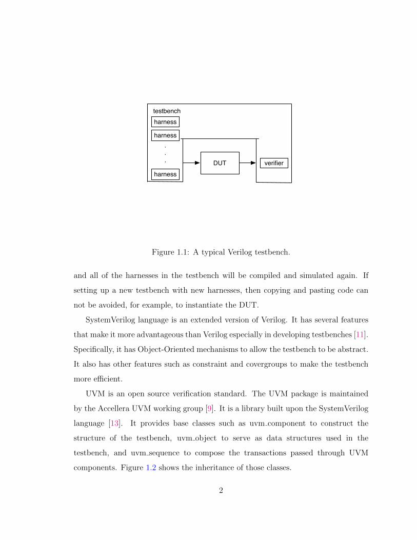
UVM is an open source verification standard. The UVM package is maintained
by the Accellera UVM working group [9]. It is a library built upon the SystemVerilog
language [13]. It provides base classes such as uvm component to construct the
structure of the testbench, uvm object to serve as data structures used in the
testbench, and uvm sequence to compose the transactions passed through UVM
components. Figure 1.2 shows the inheritance of those classes.
2
uvm_object
uvm_report_object
uvm_component
uvm_transaction
uvm_sequence_item
uvm_sequence
uvm_monitor
uvm_env uvm_driver
uvm_sequencer
uvm_test uvm_agent
uvm_scoreboard
Figure 1.2: Inheritance of UVM classes.
3
sequencer driver
monitorconfigAgent
scoreboard coverage
enviroment
test
configagentconfig
DUT
TOP
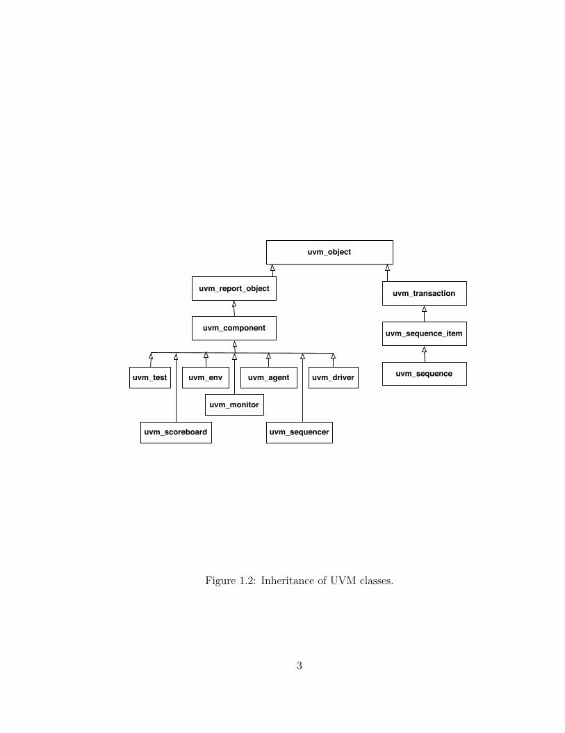
Figure 1.3: A typical UVM testbench.
UVM helps to further abstract and structure a SystemVerilog testbench. Fig-
ure 1.3 shows a typical UVM testbench. An UVM bus agent is used to drive and
monitor the signals on the interface of the DUT. With bus agents dealing with the pin-
level activities of the DUT, stimuli to the DUT are further abstracted as transactions
and sequences. UVM Transaction defines the data type sent to the agents. UVM
Sequences control how the transactions are constructed. UVM sequencer then sends
transaction from sequence to the driver inside of a UVM agent. The driver deals with
the virtual interface to drive the transaction level data to the pin level activities of the
DUT. With transaction, sequence, sequencer, and agent, the definition, construction,
transferring, and commission of stimuli are separated to allow collaboration, easy
modification, and reuse of the testbench data types and components.
1.2 Introduction to DMA
Direct Memory Access (DMA) is a mechanism that allows peripheral memory
operations that load/store data from/to main memory without the control of the
Central Processing Unit (CPU). This helps to enhance the system performance in
modern compute architecture [17]. Without DMA, for instance, if an I/O device needs
4
to write data to main memory, it should first write the data through the CPU to its
register, then the CPU will write the contents of its register to the main memory. The
processor will either do polling or wait for I/O interrupts for a small number of bytes
that are transferred from/to the device. Either way, the processor is involved in the
data movements and is blocked from performing other computing jobs. Meanwhile,
it is not efficient when transferring thousand bytes of data between the main memory
and the device, for example, a hard disk.
With DMA, the device controller can transfer large portions of data between itself
and the main memory without involving the CPU. It frees CPU from jobs such as
calculation of the memory addresses involved in the data transfer. The CPU could do
other computational work that is not related to these memory operations. In other
words, the CPU does not have to be blocked for the memory operations, which can
be too slow, reducing the system performance.
In modern computer systems, the DMA method is widely used in I/O devices
such as network cards and disk drives. The DMA method is also used in General-
purpose Graphic Processing Unit (GPGPU) accelerator technology such as [4]. Since
Field-Programmable Gate Arrays (FPGAs) are also popular as general-purpose
computational accelerators, a DMA module is used to facilitate the communication
between the FPGA and the host machine [1]. Major FPGA venders such as Altera
(bought by Intel in 2015) and Xilinx both provide their own DMA IP cores to facilitate
user designs [5, 2]. The open source projects, Riffa [14] and Riffa2.0 [15] that focus on
high performance data transfer between host main memory and FPGA accelerators,
also use a DMA module to enhance performance.
1.3 Goal of Research
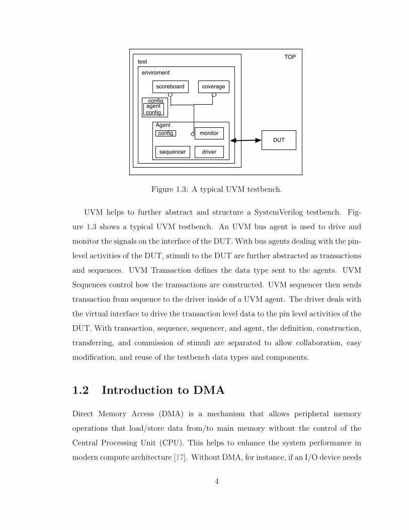
Figure 1.4 gives a general application example with a DMA module on an FPGA
which serves as an accelerator to the host machine. User logic on the device is to
process data read from the main memory on the host side. Results are sent from the
5
DMA Module
User Logic or Device Logic
Bus Module
FPGA
DMA memory
Driver and Libs
Host Application
Main Mem
Host machine
bus link
Figure 1.4: An application example with DMA module.
FPGA to the host machine. The DMA module connects a bus module and the user
logic. The bus module can be, for instance, a PCIe module. The FPGA is connected
with the host machine via physical bus links. On the host machine, proper drivers and
applications reside in the main memory. Memory dedicated for the DMA operations
between the host machine and the FPGA is pre-allocated on the host machine as
well.
DMA modules are widely used and the process of verification of the DMA core of
those designs and implementations is critical. Leveraging open source projects that
provide functional DMA cores such as [10], the design of an application such as that
shown in Figure 1.4 becomes less time-consuming. However, the original verification
of [10] is implemented with Verilog, and lacks reusability. Before we can fully trust
the design and map it onto our own platform, a thorough study and verification of this
DMA core is helpful. Using SystemVerilog and the UVM library to set up a reusable
and efficient verification framework for the DMA core will benefit both design and
further verification of the whole application system such as shown in Figure 1.4.
This thesis focuses on setting up a reusable UVM testbench for an open
6
source DMA core obtained from opencores.org [10]. The testbench is coded with
SystemVerilog and the UVM library, and is simulated with QuestaSim version 10.5 [6].
The rest of this thesis is organized as follows:
Chapter 2 introduces the DMA core DUT we verified with UVM. Chapter 3
presents the UVM testbench we designed. In this chapter, we first discuss the overall
architecture of the testbench. Then we present the bus agents in the testbench. After
that, we talk about two data objects we designed: the transactions and the register
abstraction layer. We describe the UVM testbench components, such as sequences,
coveragegroups, scoreboards, and tests, in the rest of Chapter 3. We present the
simulation and results in Chapter 4. We also discuss some bugs we found in the DMA
core in this chapter. We give conclusions and talk about future work in Chapter 5.
7
Chapter 2
Background
This chapter briefly introduces the DMA core to be tested. The original design is an
open source core and a detailed design specification can be obtained from [10].
2.1 Introduction
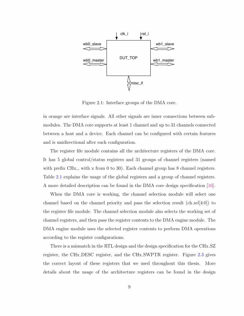
Figure 2.1 shows the interfaces of the top-level module of the DMA core. The
input and output signals can be divided into five groups, four of which are protocol
interfaces (WISHBONE v3 [12] compatible), and the fifth one is a miscellaneous
interface (misc if).
DMA operations are between the two WISHBONE master interfaces, wb0 master
and wb1 master. Reading and writing the DMA control and status registers are
through wb0 slave interface. The DMA core can work as a bridge. In the bridge mode,
signals from wb0 master will be passed to wb1 slave, while signals from wb1 master
will be passed to wb0 slave. The whole DMA core acts as only combinational logic in
the bridge mode. Verification of the bridge mode is done by the original design of the
DMA core, and is not covered by this thesis; though in our UVM testbench, it still
provides interface module designs and the corresponding bus agent for the wb1 slave
interface which are only used in the bridge mode.
Figure 2.2 shows a more detailed block-level diagram of the DMA core. Signals
8
DUT_TOP
clk_i rst_i
wb0_slave
wb0_master
wb1_slave
wb1_master
misc_if
Figure 2.1: Interface groups of the DMA core.
in orange are interface signals. All other signals are inner connections between sub-
modules. The DMA core supports at least 1 channel and up to 31 channels connected
between a host and a device. Each channel can be configured with certain features
and is unidirectional after each configuration.
The register file module contains all the architecture registers of the DMA core.
It has 5 global control/status registers and 31 groups of channel registers (named
with prefix CHx , with x from 0 to 30). Each channel group has 8 channel registers.
Table 2.1 explains the usage of the global registers and a group of channel registers.
A more detailed description can be found in the DMA core design specification [10].
When the DMA core is working, the channel selection module will select one
channel based on the channel priority and pass the selection result (ch sel[4:0]) to
the register file module. The channel selection module also selects the working set of
channel registers, and then pass the register contents to the DMA engine module. The
DMA engine module uses the selected register contents to perform DMA operations
according to the register configurations.
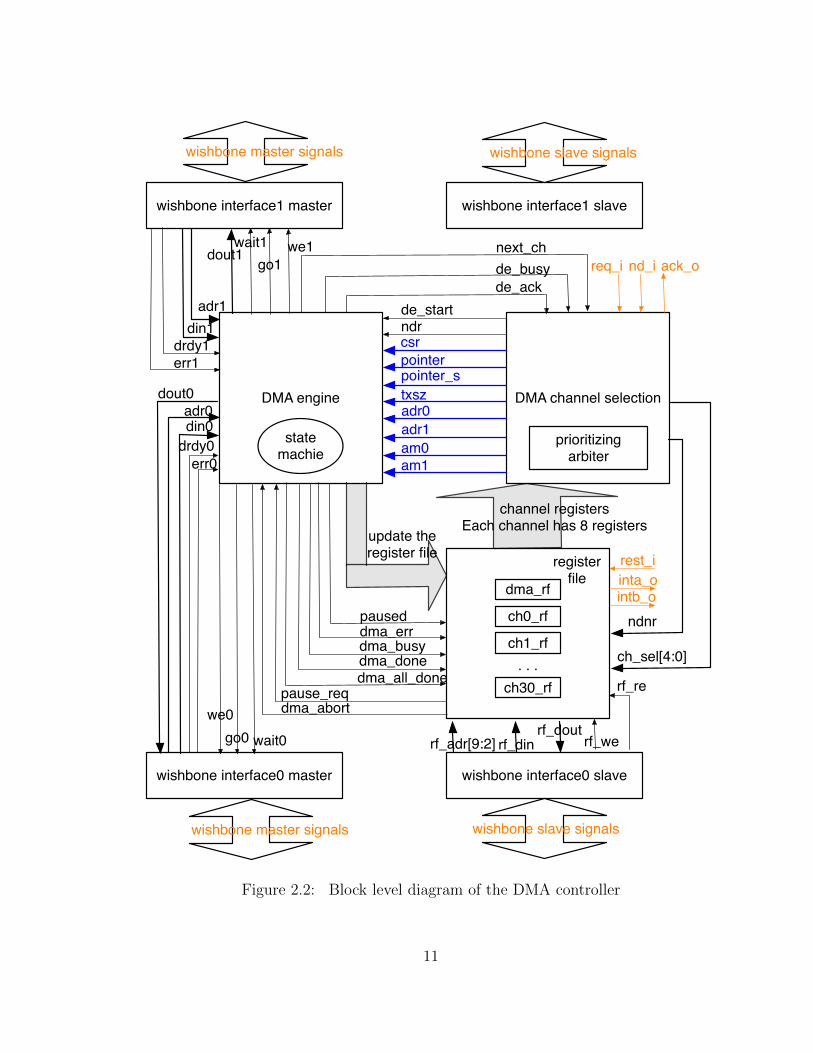
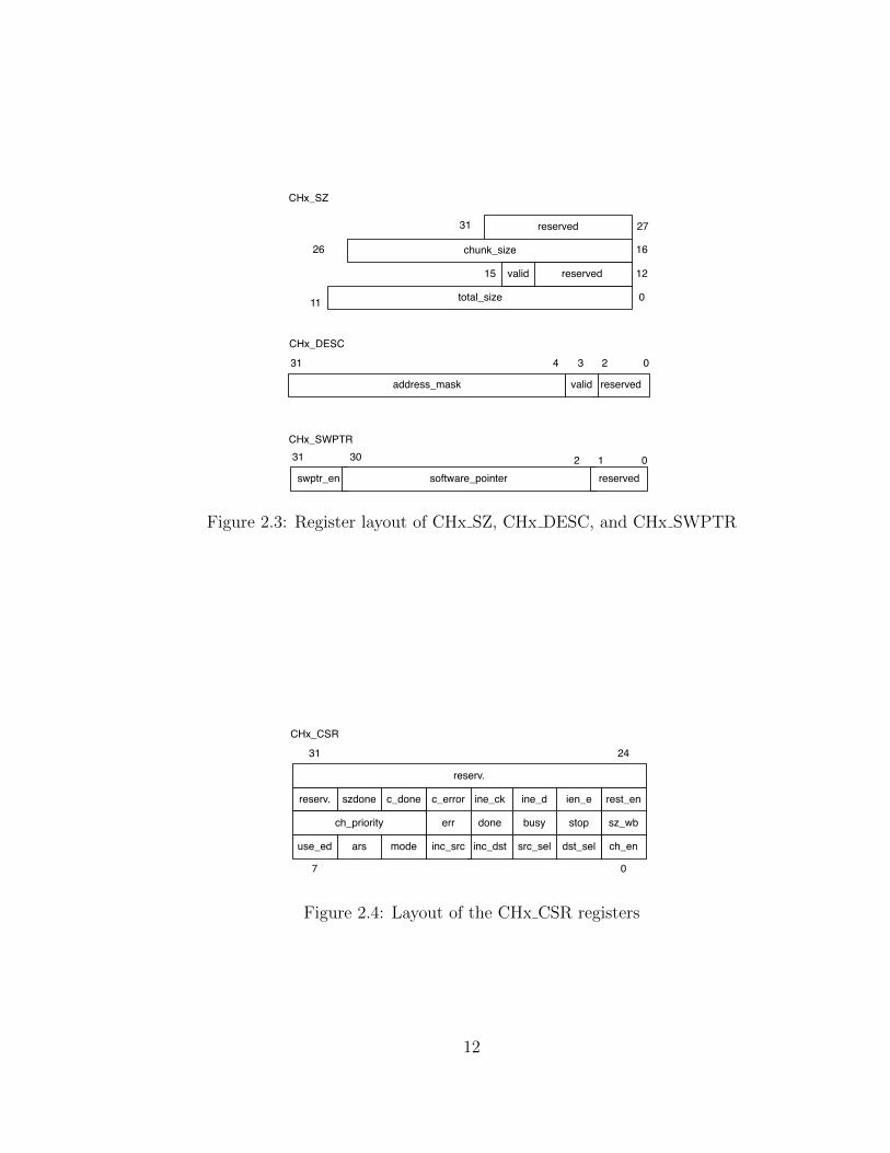
There is a mismatch in the RTL design and the design specification for the CHx SZ
register, the CHx DESC register, and the CHx SWPTR register. Figure 2.3 gives
the correct layout of these registers that we used throughout this thesis. More
details about the usage of the architecture registers can be found in the design
9
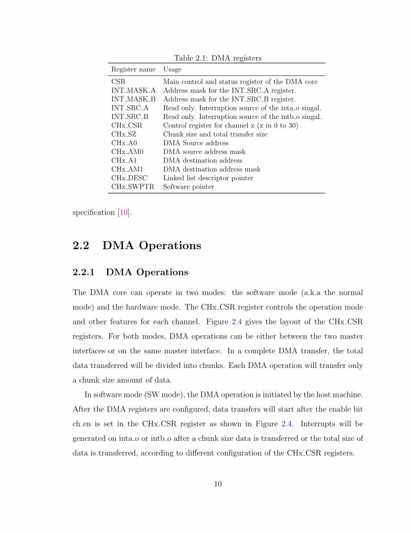
Table 2.1: DMA registers
Register name Usage
CSR Main control and status register of the DMA coreINT MASK A Address mask for the INT SRC A register.INT MASK B Address mask for the INT SRC B register.INT SRC A Read only. Interruption source of the inta o singal.INT SRC B Read only. Interruption source of the intb o singal.CHx CSR Control register for channel x (x in 0 to 30)CHx SZ Chunk size and total transfer sizeCHx A0 DMA Source addressCHx AM0 DMA source address maskCHx A1 DMA destination addressCHx AM1 DMA destination address maskCHx DESC Linked list descriptor pointerCHx SWPTR Software pointer
specification [10].
2.2 DMA Operations
2.2.1 DMA Operations
The DMA core can operate in two modes: the software mode (a.k.a the normal
mode) and the hardware mode. The CHx CSR register controls the operation mode
and other features for each channel. Figure 2.4 gives the layout of the CHx CSR
registers. For both modes, DMA operations can be either between the two master
interfaces or on the same master interface. In a complete DMA transfer, the total
data transferred will be divided into chunks. Each DMA operation will transfer only
a chunk size amount of data.
In software mode (SW mode), the DMA operation is initiated by the host machine.
After the DMA registers are configured, data transfers will start after the enable bit
ch en is set in the CHx CSR register as shown in Figure 2.4. Interrupts will be
generated on inta o or intb o after a chunk size data is transferred or the total size of
data is transferred, according to different configuration of the CHx CSR registers.
10
DMA channel selectionDMA engine
de_startndrcsrpointerpointer_stxszadr0adr1am0am1
de_busyde_ack
next_chreq_i nd_i ack_o
channel registersEach channel has 8 registers
ch0_rf
ch1_rf
ch30_rf. . .
register file inta_o
intb_o
wishbone interface0 slave
rf_adr[9:2] rf_dinrf_dout
rf_we
rf_re
ch_sel[4:0]
ndnr
update the register file
pauseddma_errdma_busydma_donedma_all_done
pause_reqdma_abort
state machie
prioritizing arbiter
dma_rf
wishbone interface0 master
wait0go0we0
err0drdy0din0adr0
dout0
wishbone master signals wishbone slave signals
rest_i
wishbone interface1 master wishbone interface1 slave
wait1go1
we1dout1
adr1din1
drdy1err1
wishbone master signals wishbone slave signals
Figure 2.2: Block level diagram of the DMA controller
11
CHx_SZ
31 reserved 27
total_size 011
chunk_size
reserved 1215
1626
valid
swptr_en
CHx_DESC
address_mask reserved
031 3 2
CHx_SWPTR
software_pointer reserved030 2 131
valid
4
Figure 2.3: Register layout of CHx SZ, CHx DESC, and CHx SWPTR
CHx_CSR
dst_sel ch_eninc_dst src_selmode inc_srcuse_ed ars
07
stop sz_wbdone busyerr
ien_e rest_enine_ck ine_dc_done c_errorreserv. szdone
ch_priority
2431
reserv.
Figure 2.4: Layout of the CHx CSR registers
12
In hardware mode (HW mode), the DMA operation is initiated by the device.
After the DMA registers are configured, data transfer will start after the device
asserts the dma req i signal on the misc if interface for corresponding channels. For
every chunk size of data transferred, the DMA core will assert a dma ack o signal on
the misc if interface for the operating channel for one bus clock cycle. The dma req i
is asserted during the DMA operation, and the device can either toggle the dma req i
and re-issue it again to transfer the next chunk size of data, or the device can keep it
being asserted for a back-to-back DMA transfer.
For both SW mode and HW mode, for each DMA transfer on a channel, the DMA
core can choose to use the DMA channel registers, which store information such as the
transfer direction, source address, destination address, data chunk size, total transfer
size, etc., to guide the transfer; or it can use the Linked List Descriptors, as known
as External Descriptors (ED), which are stored in the memory connected with the
wb0 master interface to guide the transfer. The address of the ED is configured in
the CHx DESC register for channel x, with x in 0 to 30.
2.2.2 Other Functionality
Other functionalities of the DMA core are also configurable via the CHx CSR
registers, such as the priority of the DMA channel, whether interruption is enabled for
the channel or not, whether using the ED or not, etc. The status of the DMA channel
can also be read from the CHx CSR register. A detailed bit map of the CHx CSR
register can be found in the fourth chapter of the design specification [10].
2.2.3 Host and Device Memory Organization
The memory for DMA operations on the host and device side can be organized into
circular buffers. For this organization, the source/destination address mask registers
(CHx AM0/CHx AM1) are used to make sure the address will not go beyond the
last entry of the buffer. Except for the circular buffer, the host side memory can also
13
be organized as a FIFO buffer. The software pointer register (CHx SWPTR) is then
used to record the last memory address that the software has accessed. Host software
is responsible for updating the CHx SWPTR register. Verification of the FIFO mode
is not covered by this thesis.
2.3 Conclusions
In this chapter, we introduced the open source DMA core we are going to verify. We
briefly talked about the functionality of the sub-modules of the DMA core, as well as
the architecture registers. We then introduced the DMA operation modes configured
through the channel control and status registers. In the next chapter, we will describe
the UVM testbench we built to verify this DMA core.
14
Chapter 3
UVM Testbench Design
This chapter describes the details of the UVM testbench design.
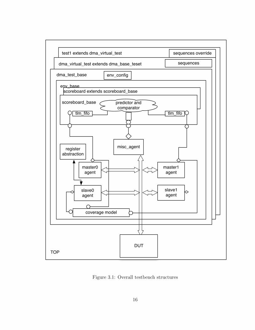
3.1 Overall Structures
The overall structures of the testbench are shown in Figure 3.1. Each group of
interface has its own bus agent. Inside of each agent, it has a driver, which drive the
sequence item onto the bus that connects the DUT and the agent; and a monitor,
which monitors the pin level activities on the bus, and then converts these activities
to transaction items, and also sends the transaction items to upper level UVM
components through analysis port and export.
In the base test, it configures the base type environment with a configuration
object. It also instantiates a register model that used in the testbench. A virtual
test, which extends the base test, sets up all the base type sequences. Those base
type sequences control the order of generated data that will eventually sent to the
DUT through virtual interfaces. In different tests, different sequences will override
the base type sequence in the virtual test.
The environment composes the main architecture of the testbench. It instantiates
all the bus agents, scoreboards, coveragegroups, register adapter and predictor. It
uses its configuration object to configure other configuration objects in bus agents,
15
master0agent
misc_agent
slave0agent
register abstraction
master1agent
slave1agent
env_config
env_base
sequences
dma_test_base
scoreboard extends scoreboard_base
test1 extends dma_virtual_test sequences override
scoreboard_base
tlm_fifo tlm_fifo
predictor and comparator
coverage model
DUTTOP
dma_virtual_test extends dma_base_teset
Figure 3.1: Overall testbench structures
16
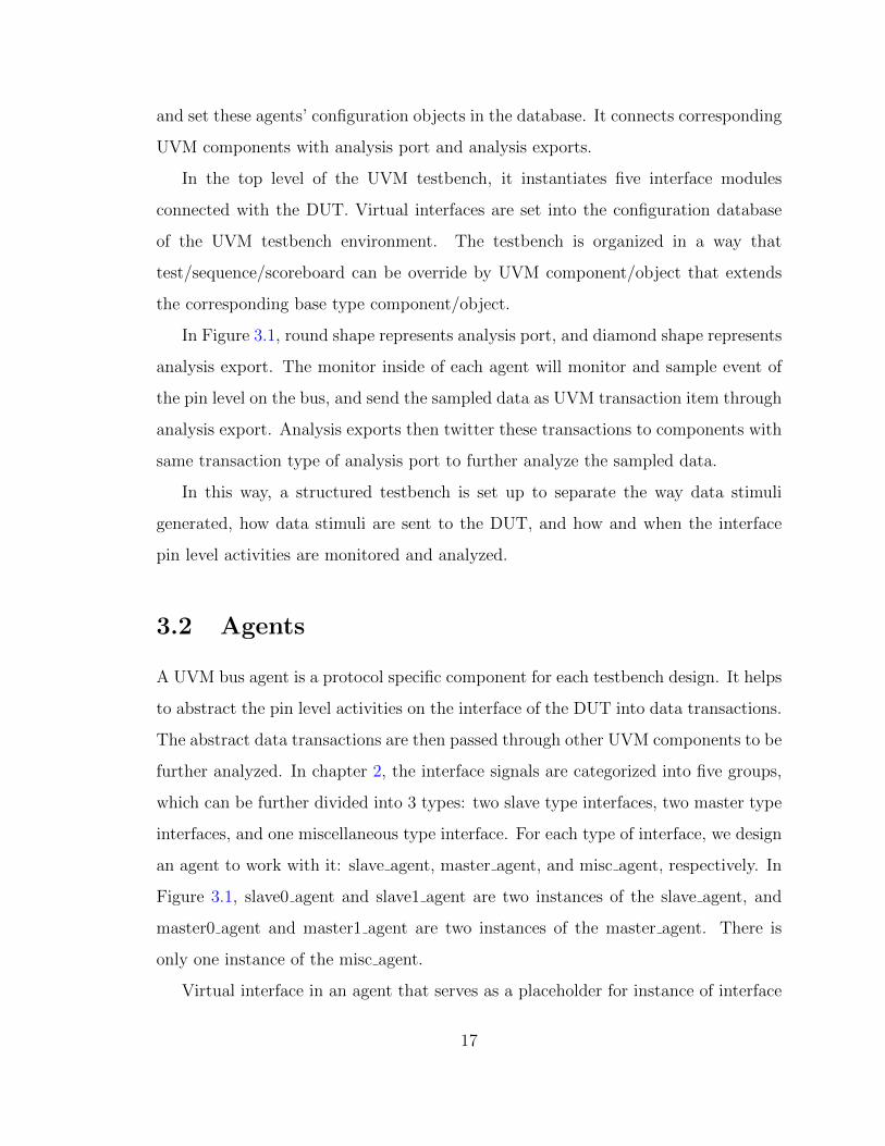
and set these agents’ configuration objects in the database. It connects corresponding
UVM components with analysis port and analysis exports.
In the top level of the UVM testbench, it instantiates five interface modules
connected with the DUT. Virtual interfaces are set into the configuration database
of the UVM testbench environment. The testbench is organized in a way that
test/sequence/scoreboard can be override by UVM component/object that extends
the corresponding base type component/object.
In Figure 3.1, round shape represents analysis port, and diamond shape represents
analysis export. The monitor inside of each agent will monitor and sample event of
the pin level on the bus, and send the sampled data as UVM transaction item through
analysis export. Analysis exports then twitter these transactions to components with
same transaction type of analysis port to further analyze the sampled data.
In this way, a structured testbench is set up to separate the way data stimuli
generated, how data stimuli are sent to the DUT, and how and when the interface
pin level activities are monitored and analyzed.
3.2 Agents
A UVM bus agent is a protocol specific component for each testbench design. It helps
to abstract the pin level activities on the interface of the DUT into data transactions.
The abstract data transactions are then passed through other UVM components to be
further analyzed. In chapter 2, the interface signals are categorized into five groups,
which can be further divided into 3 types: two slave type interfaces, two master type
interfaces, and one miscellaneous type interface. For each type of interface, we design
an agent to work with it: slave agent, master agent, and misc agent, respectively. In
Figure 3.1, slave0 agent and slave1 agent are two instances of the slave agent, and
master0 agent and master1 agent are two instances of the master agent. There is
only one instance of the misc agent.
Virtual interface in an agent that serves as a placeholder for instance of interface
17
uvm_sequence_item
wb_bus_item misc_item
Figure 3.2: Transactions
that connects the agent with the DUT. SystemVerilog interface modules are designed
for each type of interfaces of the DUT. We name the SystemVerilog interfaces
accordingly with the functionality of the interfaces of the DUT. For example, a slave
interface will connect a slave agent to the slave type interface signals of the DUT.
The design of slave interface and misc interface is straightforward. In the design
of master interface, a memory model is designed to serve as the main memory of the
host for DMA read and write operations.
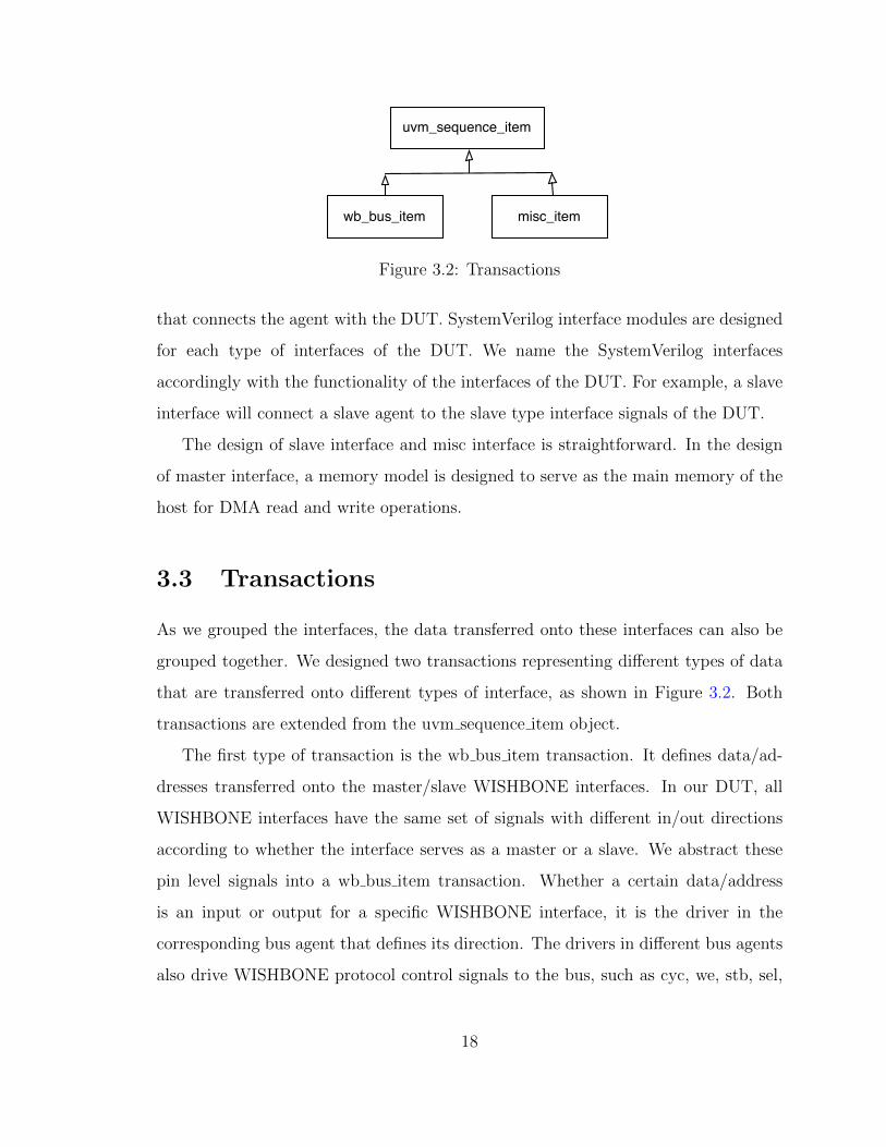
3.3 Transactions
As we grouped the interfaces, the data transferred onto these interfaces can also be
grouped together. We designed two transactions representing different types of data
that are transferred onto different types of interface, as shown in Figure 3.2. Both
transactions are extended from the uvm sequence item object.
The first type of transaction is the wb bus item transaction. It defines data/ad-
dresses transferred onto the master/slave WISHBONE interfaces. In our DUT, all
WISHBONE interfaces have the same set of signals with different in/out directions
according to whether the interface serves as a master or a slave. We abstract these
pin level signals into a wb bus item transaction. Whether a certain data/address
is an input or output for a specific WISHBONE interface, it is the driver in the
corresponding bus agent that defines its direction. The drivers in different bus agents
also drive WISHBONE protocol control signals to the bus, such as cyc, we, stb, sel,
18
ack, err, and rty, accordingly. Listing 3.1 is the code for the wb bus item transaction.
Listing 3.1: wb bus item class code
1 class wb_bus_item extends uvm_sequence_item;2 ‘uvm_object_utils(wb_bus_item)3 typedef enum {READ, WRITE, BLK_RD, BLK_WR, RMW, NO_OP}
transac_type_e;4 rand transac_type_e m_type;5 typedef enum {UNKNOWN, ACK, RTY, ERR, TIMEOUT} status_e;6 status_e m_status;7 rand bit [31:0] addr;8 rand bit [31:0] data_o;9 rand bit [31:0] data_i;10 function new(string name="wb_bus_item ");11 super.new(name);12 endfunction: new13 /*do_copy(), do_compare(), do_print, cover2string(),do_record(),14 do_pack, do_unpack not shown*/15 endclass:wb_bus_item
Listing 3.2: misc item class code
1 class misc_item extends uvm_sequence_item;2 ‘uvm_object_utils(misc_item)3 rand bit [30:0] dma_req;4 rand bit [30:0] dma_nd;5 rand bit [30:0] dma_rest;6 bit [30:0] dma_ack;7 bit inta;8 bit intb;9 int item_id;10 function new(string name="misc_item");11 super.new(name);12 endfunction13 /*do_copy(), do_compare(), do_print, cover2string(),do_record(),
do_pack, do_unpack*/14 endclass:misc_item
The second type of data transaction is the misc item transaction. In this
transaction, other than the interface signals, it also has a counter to record the item
ID. When the counter reaches zero, the misc agent driver will de-assert the dma req i
signal on the bus. Listing 3.2 gives the code of the misc item transaction.
19
offset Reg/Block
0x000 csr
0x004 int_mask_a
0x008 int_mask_b
0x00c int_src_a
0x010 int_src_b
0x020 ch0_blk map
0x040 ch1_blk map
0x3e0 ch31_blk map
reg map
.
.
.
agent adapter handle
sequencer handle
0x04 ch0_sz0x08 ch0_a00x0c ch0_am00x10 ch0_a10x14 ch0_am10x18 ch0_desc0x1c ch0_swptr
offset channel reg0x00 ch0_csr
Figure 3.3: Top-level register block and map design
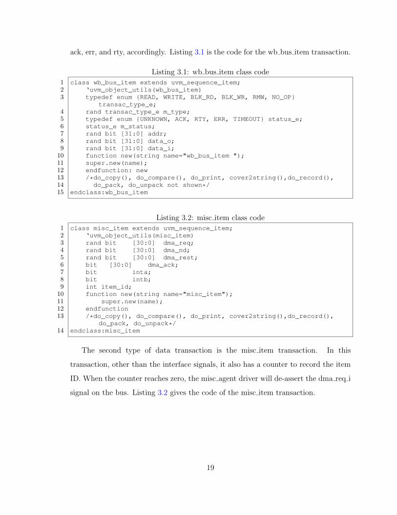
3.4 Register Level Abstraction
UVM provides a standard base class to be extended and to build particular register
level abstraction layer for the testbench [16]. Those shadow registers in the testbench
environment can store the values that are written/read to/from the registers in the
DUT. The register abstraction layer can also map the shadow registers to its bus
address. Registers can be grouped together as a register block, and further multiple
register blocks that have the same layout could be built by assigning different base
addresses to the instance of that register block.
Figure 3.3 shows the top-level register block organization and the map configura-
tion used in our testbench environment. Channel registers are organized as sub-blocks
within the top-level register block. Each sub-block is assigned with an offset address.
Figure 3.4 shows how components are connected in the base type environment.
To be concise, it only displays components that are related to the register level
abstraction layer.
20
s0_agent_cfg
s0_monitor
s0_drivers0_seqencer
slave0_agent
slave0_vif
registers
sequencerhandler
dma_reg_block
register sequences
reg2wb_adpater
base_env
env_cfg
adapterhandler
reg_mapscoreboard
predictor
coverage
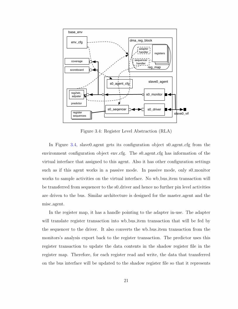
Figure 3.4: Register Level Abstraction (RLA)
In Figure 3.4, slave0 agent gets its configuration object s0 agent cfg from the
environment configuration object env cfg. The s0 agent cfg has information of the
virtual interface that assigned to this agent. Also it has other configuration settings
such as if this agent works in a passive mode. In passive mode, only s0 monitor
works to sample activities on the virtual interface. No wb bus item transaction will
be transferred from sequencer to the s0 driver and hence no further pin level activities
are driven to the bus. Similar architecture is designed for the master agent and the
misc agent.
In the register map, it has a handle pointing to the adapter in-use. The adapter
will translate register transaction into wb bus item transaction that will be fed by
the sequencer to the driver. It also converts the wb bus item transaction from the
monitors’s analysis export back to the register transaction. The predictor uses this
register transaction to update the data contents in the shadow register file in the
register map. Therefore, for each register read and write, the data that transferred
on the bus interface will be updated to the shadow register file so that it represents
21
the up-to-date contents of the real architecture registers in the DUT.
Registers in the DUT can be access either by front door access method or back
door access method [7]. In front door access method, tests access architecture registers
by generating proper bus operations to a specific register address to write or read it.
The method can be used to verify the correctness of bus transactions, but it consumes
a large simulation time to populate value to and from the DUT. In modern design and
verification, it is normal for a DUT to have hundreds of registers. In this case, front
door access could be too slow to be effective. In back door access method, registers
are accessed directly in zero simulation time. In Verilog, this is done by hierarchical
reference to the HDL code of the DUT, which could be hard to manage and reuse
in testbench design. UVM has a back door access feature in the register abstraction
layer. We add back door access to all registers in our register model. We further show
the simulation time difference of these two types of access methods in Chapter 4. In
our testbench design, we use back door access in our scoreboard to save simulation
time, mean well, to serve as a reference design.
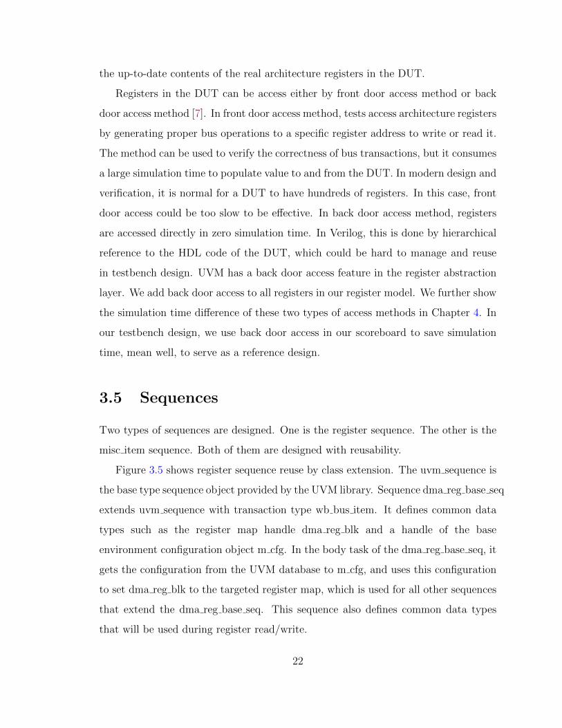
3.5 Sequences
Two types of sequences are designed. One is the register sequence. The other is the
misc item sequence. Both of them are designed with reusability.
Figure 3.5 shows register sequence reuse by class extension. The uvm sequence is
the base type sequence object provided by the UVM library. Sequence dma reg base seq
extends uvm sequence with transaction type wb bus item. It defines common data
types such as the register map handle dma reg blk and a handle of the base
environment configuration object m cfg. In the body task of the dma reg base seq, it
gets the configuration from the UVM database to m cfg, and uses this configuration
to set dma reg blk to the targeted register map, which is used for all other sequences
that extend the dma reg base seq. This sequence also defines common data types
that will be used during register read/write.
22
uvm_sequence #(wb_bus_item)
ch_csr_seq
dma_reg_base_seqdma_reg_blkm_cfgcommon data types
body task ch_common_regs_seq
ch_desc_seq
ch_csr_sw_seq
ch_csr_swp_ed_seq
ch_csr_hw_seq
ch_csr_hw_ed_seq
dma_enable_seq
Figure 3.5: Inheritance of register sequence
uvm_sequence #(misc_item)
misc_base_seq
misc_seq misc_nd_seq misc_rest_seq
Figure 3.6: Inheritance of misc item sequence
The sequence of ch csr seq only defines a loop function inside of its body task. It
defines how data are written to the CHx CSR registers. The real sequences that sent
to the sequencer are the ones that extend the ch csr seq sequence. These sequences
provide specific data to be written to the CHx CSR registers, as well as number
of channels in use. In the body task of these extended sequences, it only calls
super.body() to write the registers through bus operations. With class extension,
testbench can be more organized and reusable and it reduces copy/paste as much as
possible.
Figure 3.6 shows the inheritance relationship of the misc item sequence. The
misc item sequence is used when the DMA core is configured to operate in HW mode
or when interruption is enabled. In the dma virutal test, a base type misc base seq
23
slave0_reg_vseq virtual sequence
phase.raise_objection(this);
dma_csr_bus_seq
dma_enable_seq
ch_common_regs_seq
ch_desc_seq
ch_csr_seq
misc_seq
trigger the init_reg_done event
fork
phase.drop_objection(this);
#120000ns
join
Figure 3.7: Sequence order
sequence is used. It also calculates how many misc item transactions to be generated
by reading the CHx CSR registers in a back door mode. The misc seq sequence
is used in testing HW mode DMA with or without ED. The misc nd seq is used
in the hw dma nd test (introduced in secion 3.8). The misc rest seq is used in the
hw dma rest test (introduced in secion 3.8).
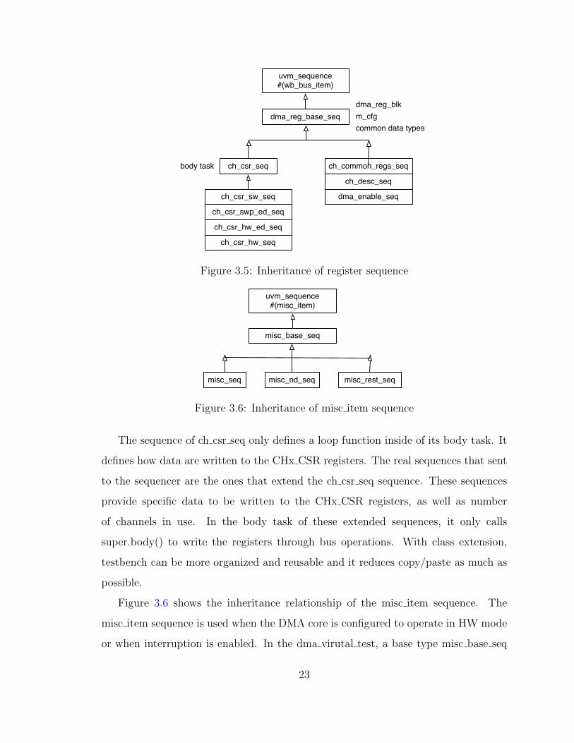
A virtual sequence is designed to group common register sequences together.
These sequences are not to be overridden in other tests. In the base type test, the
order of sequence scheduling is shown in Figure 3.7. Before starting the misc base seq,
a global SystemVerilog event is triggered to let the scoreboard know the end of
initialization of the architecture registers.
3.6 Coveragegroup
SystemVerilog covergegroups [19] are designed to capture functional coverage. Two
parts of coveragegroup are designed in our UVM testbench. One part is a dedicated
24
UVM component in the test environment. The other part is integrated in the RLA
design.
The coverage component samples item from an uvm tlm analysis fifo to record
the operations on the wb slave0 interface that if all the registers are accessed. The
FIFO is connected with analysis export on the coverage component, which is further
connected with the slave0 agent through analysis port. The coverage component also
has analysis exports to connect with the two master agents. So new design can extend
this coverage component to compose more coveragegroups for activities of the master
agents.
The functionality of the DMA core is configured by the CHx CSR registers.
Table 3.1 describes each coverage point designed in the coveragegroups in the RLA
design. Those coverage points reflect the major tests we should run during the
verification process.
3.7 Scoreboard
The scoreboard is also designed in a way that can be reused in the future. Since
DMA operation in SW mode and HW has different interactions on the interfaces,
two scoreboards, hw dma scoreboard and sw dma scorebaord, are designed for each
DMA modes separately. Both scoreboards inherit the same base type scoreboard
dma scoreboard base.
Because the write method of the analysis export completes in zero time, it cannot
guarantee the order of the transaction that is passed through the analysis port to the
scoreboard. The dma scoreboard base scoreboard uses UVM analysis FIFOs to keep
the order of the transactions that are sampled by the monitor.
In the base environment, the base type scoreboard is declared and instantiated.
The environment connects all the analysis exports with corresponding analysis
ports from the agents. In later test, extensions such as hw dma scoreboard and
sw dma scoreboard will override this base type scoreboard while maintaining the
25
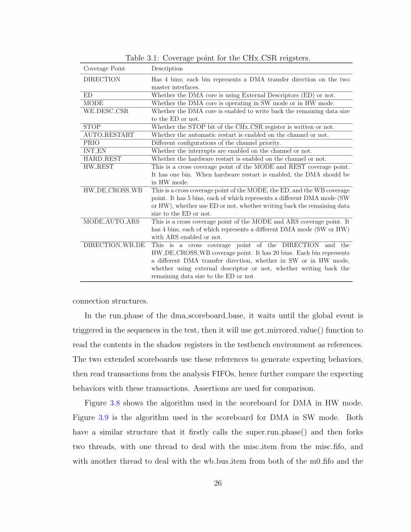
Table 3.1: Coverage point for the CHx CSR reigsters.Coverage Point Description
DIRECTION Has 4 bins; each bin represents a DMA transfer direction on the twomaster interfaces.
ED Whether the DMA core is using External Descriptors (ED) or not.MODE Whether the DMA core is operating in SW mode or in HW mode.WE DESC CSR Whether the DMA core is enabled to write back the remaining data size
to the ED or not.STOP Whether the STOP bit of the CHx CSR register is written or not.AUTO RESTART Whether the automatic restart is enabled on the channel or not.PRIO Different configurations of the channel priority.INT EN Whether the interrupts are enabled on the channel or not.HARD REST Whether the hardware restart is enabled on the channel or not.HW REST This is a cross coverage point of the MODE and REST coverage point.
It has one bin. When hardware restart is enabled, the DMA should bein HW mode.
HW DE CROSS WB This is a cross coverage point of the MODE, the ED, and the WB coveragepoint. It has 5 bins, each of which represents a different DMA mode (SWor HW), whether use ED or not, whether writing back the remaining datasize to the ED or not.
MODE AUTO ARS This is a cross coverage point of the MODE and ARS coverage point. Ithas 4 bins, each of which represents a different DMA mode (SW or HW)with ARS enabled or not.
DIRECTION WB DE This is a cross coverage point of the DIRECTION and theHW DE CROSS WB coverage point. It has 20 bins. Each bin representsa different DMA transfer direction, whether in SW or in HW mode,whether using external descriptor or not, whether writing back theremaining data size to the ED or not.
connection structures.
In the run phase of the dma scoreboard base, it waits until the global event is
triggered in the sequences in the test, then it will use get mirrored value() function to
read the contents in the shadow registers in the testbench environment as references.
The two extended scoreboards use these references to generate expecting behaviors,
then read transactions from the analysis FIFOs, hence further compare the expecting
behaviors with these transactions. Assertions are used for comparison.
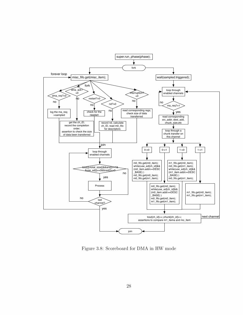
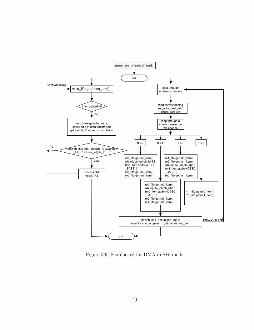
Figure 3.8 shows the algorithm used in the scoreboard for DMA in HW mode.
Figure 3.9 is the algorithm used in the scoreboard for DMA in SW mode. Both
have a similar structure that it firstly calls the super.run phase() and then forks
two threads, with one thread to deal with the misc item from the misc fifo, and
with another thread to deal with the wb bus item from both of the m0 fifo and the
26
m1 fifo, where the sm0 fifo stores transactions from the m0 agent, and the m1 fifo
stores transactions from the m1 agent.
Major difference is that the scoreboard for DMA in HW mode needs to fork
multiple threads to deal with different scenarios of the misc item transaction.
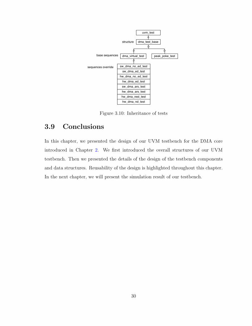
3.8 Tests
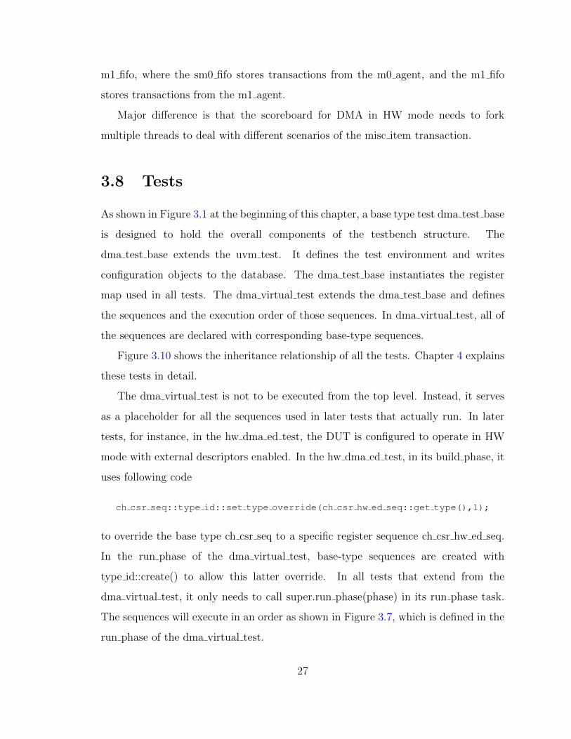
As shown in Figure 3.1 at the beginning of this chapter, a base type test dma test base
is designed to hold the overall components of the testbench structure. The
dma test base extends the uvm test. It defines the test environment and writes
configuration objects to the database. The dma test base instantiates the register
map used in all tests. The dma virtual test extends the dma test base and defines
the sequences and the execution order of those sequences. In dma virtual test, all of
the sequences are declared with corresponding base-type sequences.
Figure 3.10 shows the inheritance relationship of all the tests. Chapter 4 explains
these tests in detail.
The dma virtual test is not to be executed from the top level. Instead, it serves
as a placeholder for all the sequences used in later tests that actually run. In later
tests, for instance, in the hw dma ed test, the DUT is configured to operate in HW
mode with external descriptors enabled. In the hw dma ed test, in its build phase, it
uses following code
ch csr seq::type id::set type override(ch csr hw ed seq::get type(),1);
to override the base type ch csr seq to a specific register sequence ch csr hw ed seq.
In the run phase of the dma virtual test, base-type sequences are created with
type id::create() to allow this latter override. In all tests that extend from the
dma virtual test, it only needs to call super.run phase(phase) in its run phase task.
The sequences will execute in an order as shown in Figure 3.7, which is defined in the
run phase of the dma virtual test.
27
fork
dma_req?=0
no
log the ma_req;->sampled
dma_ack?=0
no
get the ch_iD;record the completion
order;assertion to check the size of data been transferred
interruption?=0
read corresponding regs;check size of data
transferred
no nd?=0
record nd, calculate ch_ID, read m0_fifo
for descriptors
no
restart?=0
check for the reastart
no
loop through enabled channels
tosz[i]>total_size[i]&&ars[i]==1&&use_ed[i]==0&&rest[i]==0
yes
Process
last channel?
forever loop
join
loop through enabled channels
ma_req?=1
read corresponding src_addr, dest_add,
chuck_size,etc
loop through a chunk transfer on
this channel
0->0 0->1 1->0 1->1
m0_fifo.get(m0_item);while(use_ed[ch_id]&& (m0_item.addr>=DESC_BASE) )m0_fifo.get(m0_item);m0_fifo.get(m1_item);
m0_fifo.get(m0_item);while(use_ed[ch_id]&& (m0_item.addr>=DESC_BASE) )m0_fifo.get(m0_item);m1_fifo.get(m1_item);
m1_fifo.get(m0_item);m0_fifo.get(m1_item);while(use_ed[ch_id]&& (m1_item.addr>=DESC_BASE) )m0_fifo.get(m1_item);
m1_fifo.get(m0_item);m1_fifo.get(m1_item);
tosz[ch_id]++;;chunk[ch_id]++;assertions to compare m1_itema and mo_item
next channel
yes
no
no
yes
no
join
super.run_phase(phase);
fork
misc_fifo.get(misc_item); wait(sampled.triggered);
Figure 3.8: Scoreboard for DMA in HW mode
28
interruption?=0
read corresponding regs;check size of data transferred
get the ch_ID order of completion
tosz[ch_ID]>total_size[ch_ID]&&ars[ch_ID]==1&&use_ed[ch_ID]==0
yes
Process SW mode ARS
forever looploop through
enabled channels
read corresponding src_addr, dest_add,
chuck_size,etc
loop through a chunk transfer on
this channel
0->0 0->1 1->0 1->1
m0_fifo.get(m0_item);while(use_ed[ch_id]&& (m0_item.addr>=DESC_BASE) )m0_fifo.get(m0_item);m0_fifo.get(m1_item);
m0_fifo.get(m0_item);while(use_ed[ch_id]&& (m0_item.addr>=DESC_BASE) )m0_fifo.get(m0_item);m1_fifo.get(m1_item);
m1_fifo.get(m0_item);m0_fifo.get(m1_item);while(use_ed[ch_id]&& (m1_item.addr>=DESC_BASE) )m0_fifo.get(m1_item);
m1_fifo.get(m0_item);m1_fifo.get(m1_item);
tosz[ch_id]++;;chunk[ch_id]++;assertions to compare m1_itema and mo_item
next channel
join
super.run_phase(phase);
fork
misc_fifo.get(misc_item);
no
no
Figure 3.9: Scoreboard for DMA in SW mode
29
uvm_test
dma_test_base
dma_virtual_test
structure
base sequences
sw_dma_no_ed_testsw_dma_ed_test
sequences override
peak_poke_test
hw_dma_no_ed_testhw_dma_ed_testsw_dma_ars_testhw_dma_ars_testhw_dma_rest_testhw_dma_nd_test
Figure 3.10: Inheritance of tests
3.9 Conclusions
In this chapter, we presented the design of our UVM testbench for the DMA core
introduced in Chapter 2. We first introduced the overall structures of our UVM
testbench. Then we presented the details of the design of the testbench components
and data structures. Reusability of the design is highlighted throughout this chapter.
In the next chapter, we will present the simulation result of our testbench.
30
Chapter 4
Simulations and Results
This chapter represents the test case and simulation results for the DMA core. We
will verify 4 channels of the DMA core using the UVM testbench designed in Chapter
3. The methods used in Chapter 3 and Chapter 4 can be used to further verify more
channels.
4.1 Test Cases Illustration
A DMA transfer can be started either by the host controller which is connected to the
WISHBONE interface 0, or by the user logic connected to the WISHBONE interface
1. The first type of transfer is the SW mode DMA. The other type is the HW mode
DMA. For each mode, External Linked List Descriptors (EDs) could either be used or
not according to different configuration the USE ED bit in the channel CSR register.
The external descriptors are stored in the host memory, which is attached to the
master WISHBONE interface0 of the DMA DUT.
In SW mode, the DMA transfer is initiated on a certain channel by setting the
CH EN bit of the corresponding channel CSR register. Transfer can occur either
on the same WISHBONE master interface, or between the two master WISHBONE
interfaces.
Table 4.1 gives an example of configuration of the CHx CSR register for the 4
31
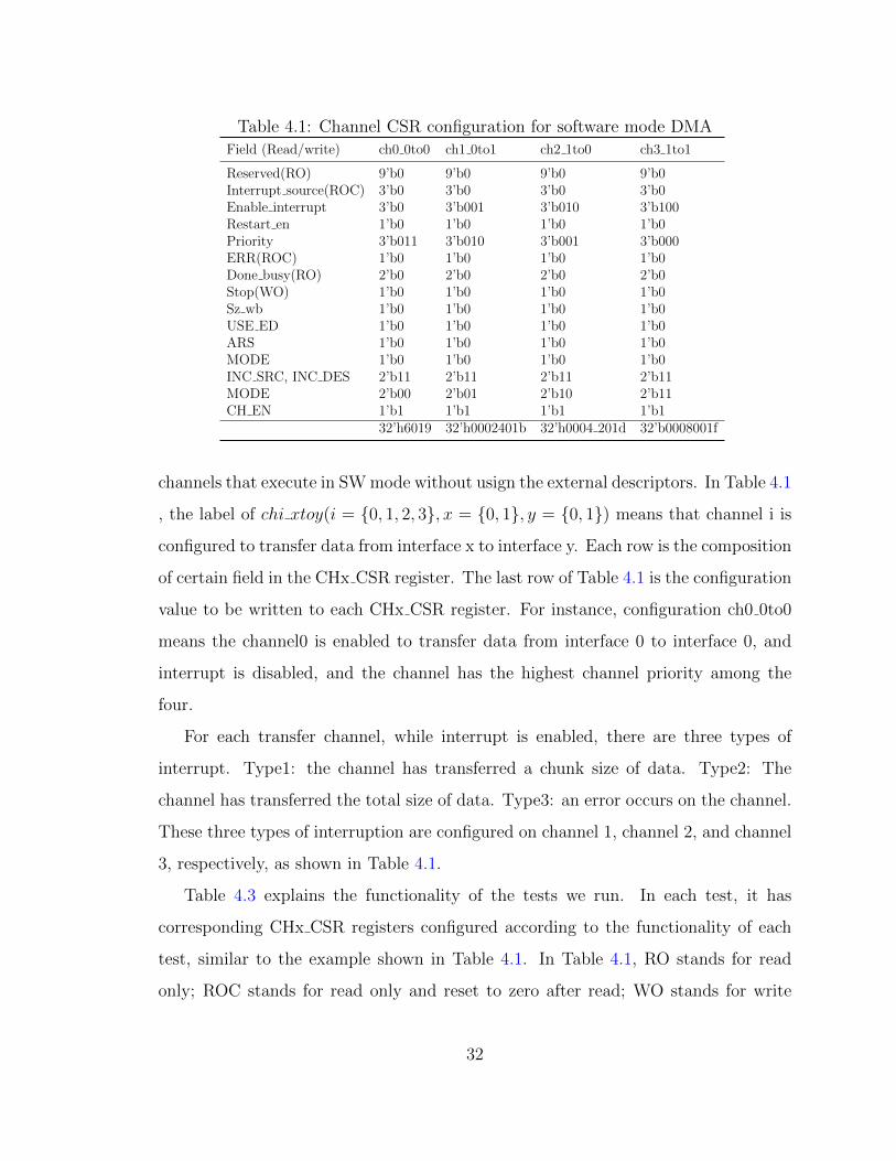
Table 4.1: Channel CSR configuration for software mode DMAField (Read/write) ch0 0to0 ch1 0to1 ch2 1to0 ch3 1to1
Reserved(RO) 9’b0 9’b0 9’b0 9’b0Interrupt source(ROC) 3’b0 3’b0 3’b0 3’b0Enable interrupt 3’b0 3’b001 3’b010 3’b100Restart en 1’b0 1’b0 1’b0 1’b0Priority 3’b011 3’b010 3’b001 3’b000ERR(ROC) 1’b0 1’b0 1’b0 1’b0Done busy(RO) 2’b0 2’b0 2’b0 2’b0Stop(WO) 1’b0 1’b0 1’b0 1’b0Sz wb 1’b0 1’b0 1’b0 1’b0USE ED 1’b0 1’b0 1’b0 1’b0ARS 1’b0 1’b0 1’b0 1’b0MODE 1’b0 1’b0 1’b0 1’b0INC SRC, INC DES 2’b11 2’b11 2’b11 2’b11MODE 2’b00 2’b01 2’b10 2’b11CH EN 1’b1 1’b1 1’b1 1’b1
32’h6019 32’h0002401b 32’h0004 201d 32’b0008001f
channels that execute in SW mode without usign the external descriptors. In Table 4.1
, the label of chi xtoy(i = {0, 1, 2, 3}, x = {0, 1}, y = {0, 1}) means that channel i is
configured to transfer data from interface x to interface y. Each row is the composition
of certain field in the CHx CSR register. The last row of Table 4.1 is the configuration
value to be written to each CHx CSR register. For instance, configuration ch0 0to0
means the channel0 is enabled to transfer data from interface 0 to interface 0, and
interrupt is disabled, and the channel has the highest channel priority among the
four.
For each transfer channel, while interrupt is enabled, there are three types of
interrupt. Type1: the channel has transferred a chunk size of data. Type2: The
channel has transferred the total size of data. Type3: an error occurs on the channel.
These three types of interruption are configured on channel 1, channel 2, and channel
3, respectively, as shown in Table 4.1.
Table 4.3 explains the functionality of the tests we run. In each test, it has
corresponding CHx CSR registers configured according to the functionality of each
test, similar to the example shown in Table 4.1. In Table 4.1, RO stands for read
only; ROC stands for read only and reset to zero after read; WO stands for write
32
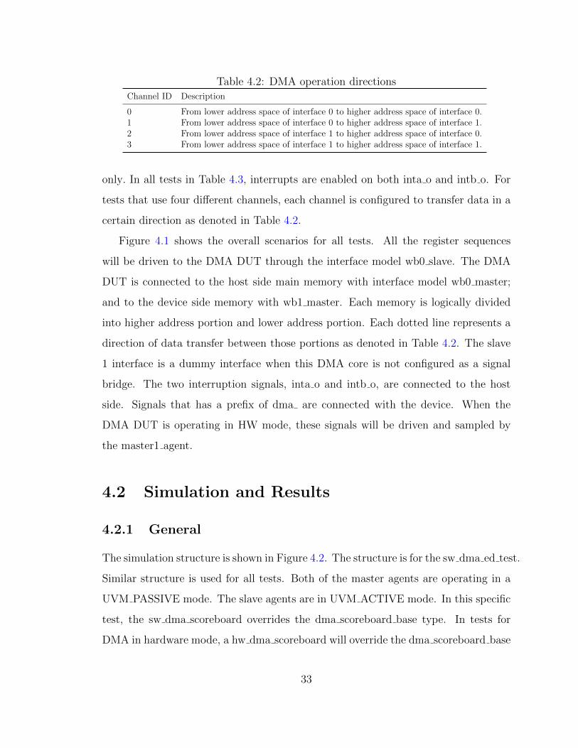
Table 4.2: DMA operation directionsChannel ID Description
0 From lower address space of interface 0 to higher address space of interface 0.1 From lower address space of interface 0 to higher address space of interface 1.2 From lower address space of interface 1 to higher address space of interface 0.3 From lower address space of interface 1 to higher address space of interface 1.
only. In all tests in Table 4.3, interrupts are enabled on both inta o and intb o. For
tests that use four different channels, each channel is configured to transfer data in a
certain direction as denoted in Table 4.2.
Figure 4.1 shows the overall scenarios for all tests. All the register sequences
will be driven to the DMA DUT through the interface model wb0 slave. The DMA
DUT is connected to the host side main memory with interface model wb0 master;
and to the device side memory with wb1 master. Each memory is logically divided
into higher address portion and lower address portion. Each dotted line represents a
direction of data transfer between those portions as denoted in Table 4.2. The slave
1 interface is a dummy interface when this DMA core is not configured as a signal
bridge. The two interruption signals, inta o and intb o, are connected to the host
side. Signals that has a prefix of dma are connected with the device. When the
DMA DUT is operating in HW mode, these signals will be driven and sampled by
the master1 agent.
4.2 Simulation and Results
4.2.1 General
The simulation structure is shown in Figure 4.2. The structure is for the sw dma ed test.
Similar structure is used for all tests. Both of the master agents are operating in a
UVM PASSIVE mode. The slave agents are in UVM ACTIVE mode. In this specific
test, the sw dma scoreboard overrides the dma scoreboard base type. In tests for
DMA in hardware mode, a hw dma scoreboard will override the dma scoreboard base
33
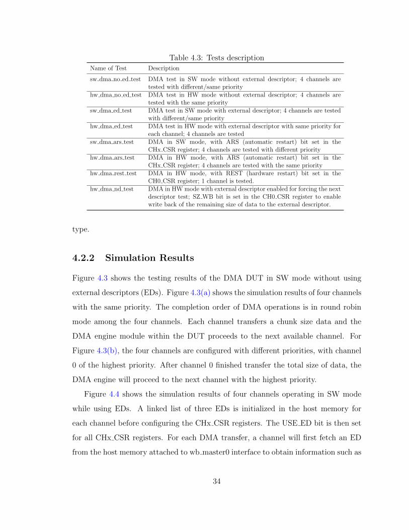
Table 4.3: Tests descriptionName of Test Description
sw dma no ed test DMA test in SW mode without external descriptor; 4 channels aretested with different/same priority
hw dma no ed test DMA test in HW mode without external descriptor; 4 channels aretested with the same priority
sw dma ed test DMA test in SW mode with external descriptor; 4 channels are testedwith different/same priority
hw dma ed test DMA test in HW mode with external descriptor with same priority foreach channel; 4 channels are tested
sw dma ars test DMA in SW mode, with ARS (automatic restart) bit set in theCHx CSR register; 4 channels are tested with different priority
hw dma ars test DMA in HW mode, with ARS (automatic restart) bit set in theCHx CSR register; 4 channels are tested with the same priority
hw dma rest test DMA in HW mode, with REST (hardware restart) bit set in theCH0 CSR register; 1 channel is tested.
hw dma nd test DMA in HW mode with external descriptor enabled for forcing the nextdescriptor test; SZ WB bit is set in the CH0 CSR register to enablewrite back of the remaining size of data to the external descriptor.
type.
4.2.2 Simulation Results
Figure 4.3 shows the testing results of the DMA DUT in SW mode without using
external descriptors (EDs). Figure 4.3(a) shows the simulation results of four channels
with the same priority. The completion order of DMA operations is in round robin
mode among the four channels. Each channel transfers a chunk size data and the
DMA engine module within the DUT proceeds to the next available channel. For
Figure 4.3(b), the four channels are configured with different priorities, with channel
0 of the highest priority. After channel 0 finished transfer the total size of data, the
DMA engine will proceed to the next channel with the highest priority.
Figure 4.4 shows the simulation results of four channels operating in SW mode
while using EDs. A linked list of three EDs is initialized in the host memory for
each channel before configuring the CHx CSR registers. The USE ED bit is then set
for all CHx CSR registers. For each DMA transfer, a channel will first fetch an ED
from the host memory attached to wb master0 interface to obtain information such as
34
register_sequences
DUT_TOP
clk_i rst_i
wb0_slave
wb0_master
wb1_slave
wb1_master
hi
lo
host_memory
hi
lo
device_memory
ch0ch1
ch2ch3
ExternalDescriptors
intb_ointa_o
[30:0] dma_rest_i
[30:0] dma_req_i
[30:0] dma_nd_i
[30:0] dma_ack_o
HW mode, device signals
Figure 4.1: Scenarios for tests
total transfer size, chuck size, source and destination addresses, the memory address
for the next descriptor in this linked list. Figure 4.4(a) and Figure 4.4(b) also show
different completion orders of DMA operations on the four channels in accordance
with the configuration of channel priorities.
Figure 4.5 shows the simulation result of the DMA DUT in HW mode without
using ED for four channels. Figure 4.6 shows a detailed simulation result for DMA in
HW mode for just one channel using one external descriptor. Each DMA operation
will transfer a chunk size of 16 words. Total 8 chunks of data are transferred for one
external descriptor. Figure 4.7 shows the DMA core in HW mode with ED enabled
for four channels. Channels are configured with the same priority in these tests.
When the ARS field of the CHx CSR register is set and no external descriptor is
used, the channel is set to operate in an auto restart mode. When current channel
successfully transferred a total size data as indicated in the CH SZ register, the
channel will automatically restart the transfer, until the ARS bit is cleared or the
STOP bit in the CH CSR register is set. In the later scenario, the DMA engine
will stop working and asserts a dm abort signal internally. If interrupt is enabled,
signal int o and/or int o will be asserted with CH SZ ERR bit set and corresponding
IN SR A and/or IN SR B is marked with the channel ID number.
35
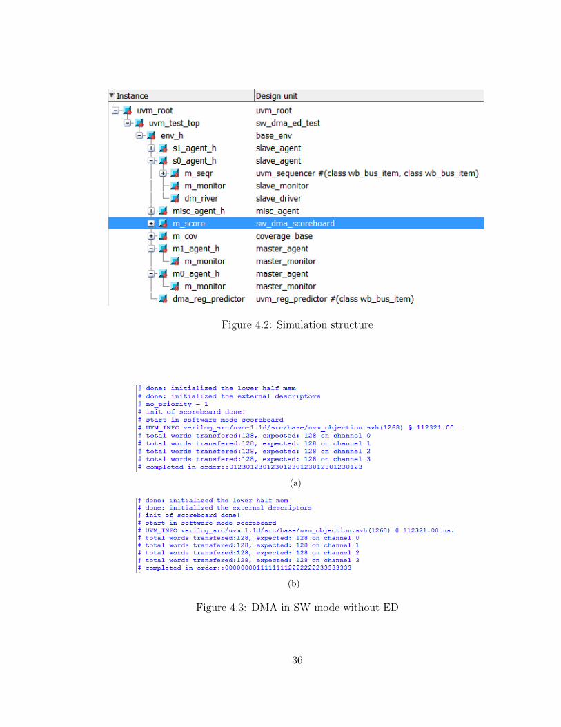
Figure 4.2: Simulation structure
(a)
(b)
Figure 4.3: DMA in SW mode without ED
36
(a)
(b)
Figure 4.4: DMA in SW mode with ED
Figure 4.5: DMA in HW mode without ED
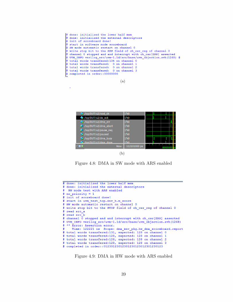
In Figure 4.8, 4 channels are enabled in SW mode with ARS bits set. After
channel 0 transferred a total size data, it automatically restarts the transfer since
it has the highest priority. After detecting the restart, the test sets the STOP
bit in the CH0 CSR register, and then the DMA DUT asserts an interrupt with
CH0 CSR[ERR] bit set. The waveform in Figure 4.8(b)shows that a dma abort signal
is asserted internally in the DUT. The DUT aborts after the STOP bit is set in the
CH0 CSR registers, which is not clearly described in the original documentation of
the design [10].
Figure 4.9 shows the test results of ARS bit set and the DUT operates in HW
37
Figure 4.6: One channel test in HW mode with ED
Figure 4.7: DMA in HW mode with ED
mode. Four channels are enabled with the same priority. After each channel completes
in a round-robin order, channel 0 repeats its previous DMA transfer. The test detects
that and asserts STOP in the CH0 CSR register. After that, interrupts assert on the
misc if interface and the DMA engine aborts.
When a DMA transfer is not finished due to some reason, the unfinished previous
transfer could be restarted in HW mode with REST bit set in CHx CSR register
and with dma rest i signal asserted on the misc interface. Figure 4.10 shows the test
result of the hardware restart operation. A total size of 128 words (8 chunks data)
needs to be transferred. After 80 (this number is a constrained random number which
is less than the total size) words are transferred on channel 0, the hardware restart
signal is issued on the misc if interface. After that, 128 words are transferred in total.
Figure 4.11 shows the result of testing the forcing next descriptor. After 4 chunks
of data transferred, dma nd i is asserted on channel 0 to force the DMA engine
aborting current external descriptor and load the next descriptor in the linked list,
38
(a)
(b)
Figure 4.8: DMA in SW mode with ARS enabled
Figure 4.9: DMA in HW mode with ARS enabled
39
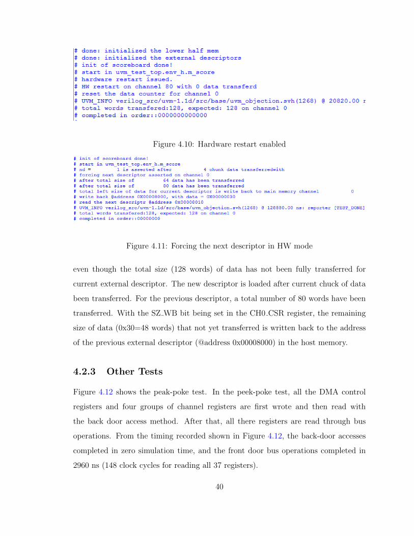
Figure 4.10: Hardware restart enabled
Figure 4.11: Forcing the next descriptor in HW mode
even though the total size (128 words) of data has not been fully transferred for
current external descriptor. The new descriptor is loaded after current chuck of data
been transferred. For the previous descriptor, a total number of 80 words have been
transferred. With the SZ WB bit being set in the CH0 CSR register, the remaining
size of data (0x30=48 words) that not yet transferred is written back to the address
of the previous external descriptor (@address 0x00008000) in the host memory.
4.2.3 Other Tests
Figure 4.12 shows the peak-poke test. In the peek-poke test, all the DMA control
registers and four groups of channel registers are first wrote and then read with
the back door access method. After that, all there registers are read through bus
operations. From the timing recorded shown in Figure 4.12, the back-door accesses
completed in zero simulation time, and the front door bus operations completed in
2960 ns (148 clock cycles for reading all 37 registers).
40
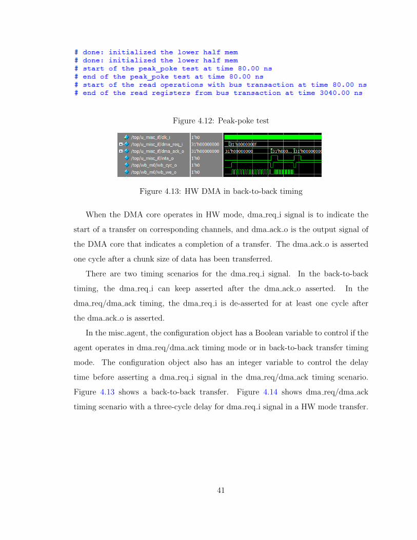
Figure 4.12: Peak-poke test
Figure 4.13: HW DMA in back-to-back timing
When the DMA core operates in HW mode, dma req i signal is to indicate the
start of a transfer on corresponding channels, and dma ack o is the output signal of
the DMA core that indicates a completion of a transfer. The dma ack o is asserted
one cycle after a chunk size of data has been transferred.
There are two timing scenarios for the dma req i signal. In the back-to-back
timing, the dma req i can keep asserted after the dma ack o asserted. In the
dma req/dma ack timing, the dma req i is de-asserted for at least one cycle after
the dma ack o is asserted.
In the misc agent, the configuration object has a Boolean variable to control if the
agent operates in dma req/dma ack timing mode or in back-to-back transfer timing
mode. The configuration object also has an integer variable to control the delay
time before asserting a dma req i signal in the dma req/dma ack timing scenario.
Figure 4.13 shows a back-to-back transfer. Figure 4.14 shows dma req/dma ack
timing scenario with a three-cycle delay for dma req i signal in a HW mode transfer.
41
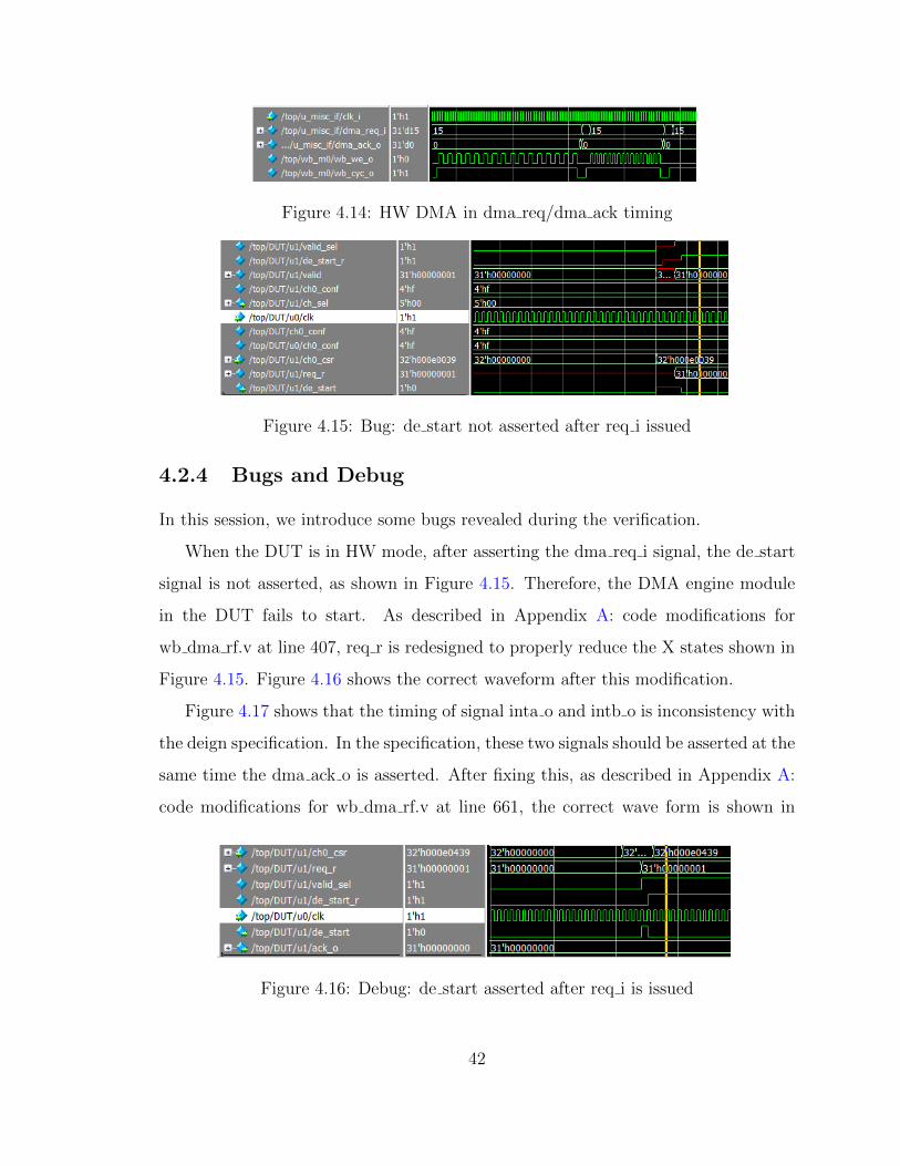
Figure 4.14: HW DMA in dma req/dma ack timing
Figure 4.15: Bug: de start not asserted after req i issued
4.2.4 Bugs and Debug
In this session, we introduce some bugs revealed during the verification.
When the DUT is in HW mode, after asserting the dma req i signal, the de start
signal is not asserted, as shown in Figure 4.15. Therefore, the DMA engine module
in the DUT fails to start. As described in Appendix A: code modifications for
wb dma rf.v at line 407, req r is redesigned to properly reduce the X states shown in
Figure 4.15. Figure 4.16 shows the correct waveform after this modification.
Figure 4.17 shows that the timing of signal inta o and intb o is inconsistency with
the deign specification. In the specification, these two signals should be asserted at the
same time the dma ack o is asserted. After fixing this, as described in Appendix A:
code modifications for wb dma rf.v at line 661, the correct wave form is shown in
Figure 4.16: Debug: de start asserted after req i is issued
42
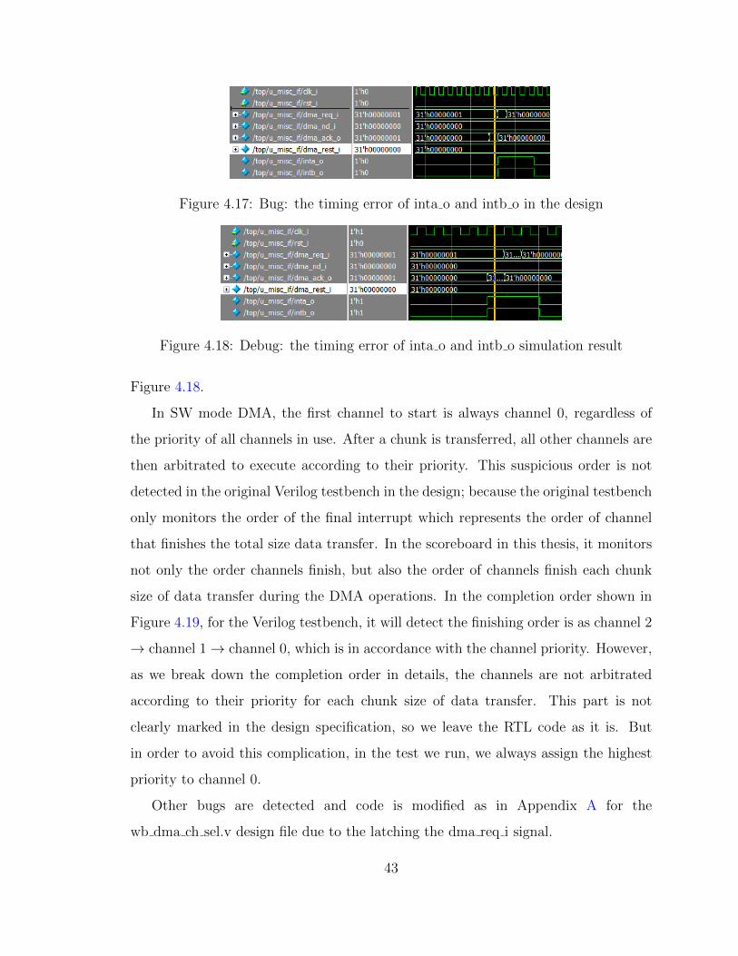
Figure 4.17: Bug: the timing error of inta o and intb o in the design
Figure 4.18: Debug: the timing error of inta o and intb o simulation result
Figure 4.18.
In SW mode DMA, the first channel to start is always channel 0, regardless of
the priority of all channels in use. After a chunk is transferred, all other channels are
then arbitrated to execute according to their priority. This suspicious order is not
detected in the original Verilog testbench in the design; because the original testbench
only monitors the order of the final interrupt which represents the order of channel
that finishes the total size data transfer. In the scoreboard in this thesis, it monitors
not only the order channels finish, but also the order of channels finish each chunk
size of data transfer during the DMA operations. In the completion order shown in
Figure 4.19, for the Verilog testbench, it will detect the finishing order is as channel 2
→ channel 1→ channel 0, which is in accordance with the channel priority. However,
as we break down the completion order in details, the channels are not arbitrated
according to their priority for each chunk size of data transfer. This part is not
clearly marked in the design specification, so we leave the RTL code as it is. But
in order to avoid this complication, in the test we run, we always assign the highest
priority to channel 0.
Other bugs are detected and code is modified as in Appendix A for the
wb dma ch sel.v design file due to the latching the dma req i signal.
43
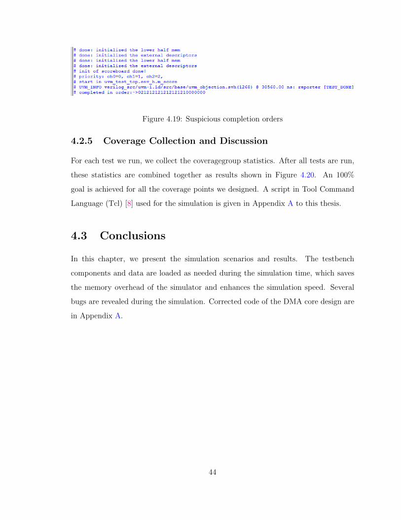
Figure 4.19: Suspicious completion orders
4.2.5 Coverage Collection and Discussion
For each test we run, we collect the coveragegroup statistics. After all tests are run,
these statistics are combined together as results shown in Figure 4.20. An 100%
goal is achieved for all the coverage points we designed. A script in Tool Command
Language (Tcl) [8] used for the simulation is given in Appendix A to this thesis.
4.3 Conclusions
In this chapter, we present the simulation scenarios and results. The testbench
components and data are loaded as needed during the simulation time, which saves
the memory overhead of the simulator and enhances the simulation speed. Several
bugs are revealed during the simulation. Corrected code of the DMA core design are
in Appendix A.
44
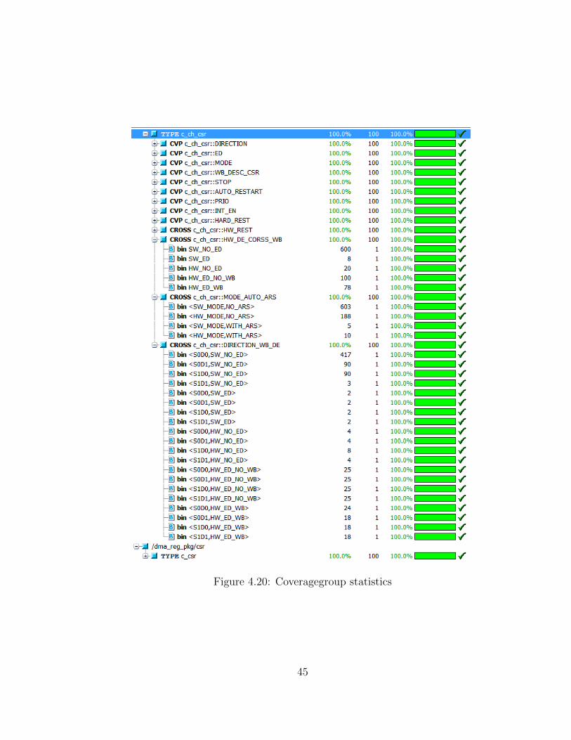
Figure 4.20: Coveragegroup statistics
45
Chapter 5
Conclusions and Future Work
As introduced in Chapter 1, a traditional Verilog testbench is a wrapper code around
the design under test (DUT). It is lack of reusability. For example, to test a new
harness, it either evolves editing the original testbench to add the harness, or it needs
to establish a new version of testbench, in which copying and pasting code of the
original testbench cannot be avoided.
To overcome the shortage of the traditional Verilog testbench, this thesis designed
a reusable UVM testbench for a DMA core obtained from [10]. Register Abstraction
Layer is designed and implemented to facilitate the verification of architecture
registers, as well as to be used as a reference model in the scoreboard component.
All sequences, tests, and scoreboards are designed with OOP feature to allow future
reuse. Coverage groups are designed to monitor the effectiveness of the tests. We
ran the simulation with four channel’s configuration and with Questasim 10.5c [6].
With the verification, we revealed several bugs in the DMA core design and corrected
the bugs as shown in Appendix A. We also pointed out that there is a mismatch
between the simulation behavior and the design specification when different priorities
are assigned onto different DMA channels.
In [3], it proposed an FPGA testing environment for the same DMA Core we tested
with our UVM testbench. Compared to the FPGA test environment, our testbench
46
uses the minimal resources before mapping the design to the more expensive and
complex FPGA platform. Our testbench also features reusability for future usage
and to allow future verification of a larger design to be built upon this thesis when
the DMA core is integrated as a sub-module.
In this thesis, we learnt that, although at the very beginning of adopting the
UVM into the verification process of an application, it requires verification engineers
to make some effort to absorb the knowledge of the UVM, this effort pays itself. An
UVM testbench is well structured. It will benefit verification of large projects that
requires collaboration works. Moreover, the OOP features of the UVM enhance the
reusability of a testbench. This makes the this thesis useful for future design and
verification.
Future work including further verification of the targeted DMA core which serves
both as a stand-alone design and a sub-module inside of an FPGA application.
47

Bibliography
48
[1] Altera SDK for OpenCL: Best Practices Guide. https://documentation.
altera.com/#/link/mwh1391807516407/mwh1391807494883/
en-us. 5
[2] AXI DMA Controller. http://www.xilinx.com/products/
intellectual-property/axi_dma.html. 5
[3] DMA Controller Example: Opencores Wishbone DMA Case. Dynalith Systems
Application Note DS-AN-2008-08-001. 46
[4] GPU Direct. https://developer.nvidia.com/gpudirect. 5
[5] PCI Express Avalon-MM High-Performance DMA Reference
Design. https://www.altera.com/products/
reference-designs/all-reference-designs/interface/
ref-pciexpress-avalonmm-hp.html. 5
[6] Questa Advanced Simulator. https://www.mentor.com/products/fv/
questa/. 7, 46
[7] Register Verification. http://www.testbench.in/TB_32_REGISTER_
VERIFICATION.html. 22
[8] Tool Command Language. https://www.tcl.tk. 44
[9] Universal Verification Methodology (UVM) Working Group. http://
accellera.org/activities/working-groups/uvm/. 2
[10] WISHBONE DMA/Bridge IP Core. http://opencores.org/project,
wb_dma. 6, 7, 8, 9, 10, 13, 37, 46
[11] SystemVerilog 3.1a Language Reference Manual, Accelleras Extensions to
Verilog. Accellera, 2004. 2
49
[12] WISHBONE System-on-Chip (SoC) Interconnection Architecture for Portable
IP Cores. opencores.org, revision b.3 edition, September, 2002. 8
[13] Gordon Allan, Mike Baird, Rich Edelman, Adam Erickson, Michael Horn,
Mark Peryer, Adam Rose, and Kurt Schwartz. UVM cookbook. http:
//verificationacademy.com/cookbook. 1, 2
[14] Matthew Jacobsen, Yoav Freund, and Ryan Kastner. Riffa: A reusable
integration framework for fpga accelerators. In Proceedings of the 2012 IEEE 20th
International Symposium on Field-Programmable Custom Computing Machines,
FCCM ’12, pages 216–219, Washington, DC, USA, 2012. IEEE Computer
Society. 5
[15] Matthew Jacobsen, Dustin Richmond, Matthew Hogains, and Ryan Kastner.
Riffa 2.1: A reusable integration framework for fpga accelerators. ACM Trans.
Reconfigurable Technol. Syst., 8(4):22:1–22:23, September 2015. 5
[16] Mark Litterick and Marcus Harnisch. Advanced uvm register modeling – there’s
more than one way to skin a reg. In DVCon, 2014. 20
[17] David A. Patterson and John L. Hennessy. Computer Organization and Design,
Fourth Edition, Fourth Edition: The Hardware/Software Interface (The Morgan
Kaufmann Series in Computer Architecture and Design). Morgan Kaufmann
Publishers Inc., San Francisco, CA, USA, 4th edition, 2008. 4
[18] Walden C. Rhines. Design verification challenges: Past, present and future.
DVCon U.S. 2016 Keynote. 1
[19] Ray Salemi. The UVM Primer: A Step-by-Step Introduction to the Universal
Verification Methodology. Boston Light Press, 1st edition, 2013. 24
50
Appendix
51
Appendix A
Script and Code
A.1 Simulation Script in Tcl
Listing A.1 is the Tcl script we used in the simulation. It first compiles the design
and the testbench. Each component of the testbench is compiled into a package for
reuse purpose. For each test we ran, we collected the statistics of the coverage group
we designed. Then at the end of the simulation, we combined those statistics together
to obtain the final coverage information.
Listing A.1: Simulation Script in Tcl1 #constraint2 #set UVM_HOME /uvm-1.1d/3 set RTL ./../rtl/verilog4 set SLAVE_AGENT ./../uvm_test/slave_agent5 set MASTER_AGENT ./../uvm_test/master_agent6 set MISC_AGENT ./../uvm_test/misc_agent7 set REG_MODEL ./../uvm_test/dma_reg_pkg8 set MEM_MODEL ./../uvm_test/dma_mem_pkg9 set ENV_MODEL ./../uvm_test/env10 set TRANS ./../uvm_test/transactions11 set SEQS ./../uvm_test/sequences12 set TESTS ./../uvm_test/test13 set VIR_SEQ ./../uvm_test/virtual_sequences14 set TOP ./../uvm_test/15 set MACRO ./../uvm_test/16 vlib work1718 #build19 vlog +incdir+$RTL $RTL/*.v +acc +cover=sbcef20 vlog $SLAVE_AGENT/wb_slave_if.sv -timescale 1ns/10ps
52
21 vlog $MASTER_AGENT/wb_master_if.sv +incdir+$TOP -timescale 1ns/10ps22 vlog $MISC_AGENT/misc_if.sv -timescale 1ns/10ps23 vlog +incdir+$TRANS $TRANS/transactions_pkg.sv24 vlog +incdir+$SLAVE_AGENT $SLAVE_AGENT/slave_agent_pkg.sv25 vlog +incdir+$MASTER_AGENT $MASTER_AGENT/master_agent_pkg.sv26 vlog -permissive +incdir+$MISC_AGENT +incdir+$MACRO $MISC_AGENT/
misc_agent_pkg.sv27 vlog +incdir+$REG_MODEL $REG_MODEL/dma_reg_pkg.sv28 vlog -permissive +incdir+$ENV_MODEL +incdir+$MACRO $ENV_MODEL/
dma_env_pkg.sv29 vlog +incdir+$SEQS +incdir+$TOP $SEQS/dma_test_sequence_pkg.sv30 vlog +incdir+$VIR_SEQ $VIR_SEQ/virtual_seq_pkg.sv31 vlog +incdir+$TESTS $TESTS/dma_test_lib_pkg.sv32 vlog $TOP/top.sv +acc33 #run the tcl input, which is the test name for this run34 #vsim top -coverage +UVM_TESTNAME=register_test35 #vsim top -coverage +UVM_TESTNAME=dma_base_test36 #vsim top -coverage +UVM_TESTNAME=peek_poke_test3738 set NoQuitOnFinish 139 onbreak {resume}4041 vsim -novopt top -coverage +UVM_TESTNAME=sw_dma_no_ed_test42 run -all43 coverage attribute -name TESTNAME -value sw_dma_no_ed_test44 coverage save sw_dma_no_ed_test.ucdb45 vsim -novopt top -coverage +UVM_TESTNAME=sw_dma_ed_test46 run -all47 coverage attribute -name TESTNAME -value sw_dma_ed_test48 coverage save sw_dma_ed_test.ucdb49 vsim -novopt top -coverage +UVM_TESTNAME=hw_dma_no_ed_test50 run -all51 coverage attribute -name TESTNAME -value hw_dma_no_ed_test52 coverage save hw_dma_no_ed_test.ucdb53 vsim -novopt top -coverage +UVM_TESTNAME=hw_dma_ed_test54 run -all55 coverage attribute -name TESTNAME -value hw_dma_ed_test56 coverage save hw_dma_ed_test.ucdb57 vsim -novopt top -coverage +UVM_TESTNAME=sw_dma_ars_test58 run -all59 coverage attribute -name TESTNAME -value sw_dma_ars_test60 coverage save sw_dma_ars_test.ucdb61 vsim -novopt top -coverage +UVM_TESTNAME=hw_dma_ars_test62 run -all63 coverage attribute -name TESTNAME -value hw_dma_ars_test64 coverage save hw_dma_ars_test.ucdb65 vsim -novopt top -coverage +UVM_TESTNAME=hw_dma_rest_test66 run -all67 coverage attribute -name TESTNAME -value hw_dma_rest_test68 coverage save hw_dma_rest_test.ucdb69 vsim -novopt top -coverage +UVM_TESTNAME=hw_dma_nd_test170 run -all71 coverage attribute -name TESTNAME -value hw_dma_nd_test172 coverage save hw_dma_nd_test1.ucdb73 vsim -novopt top -coverage +UVM_TESTNAME=hw_dma_nd_test2
53
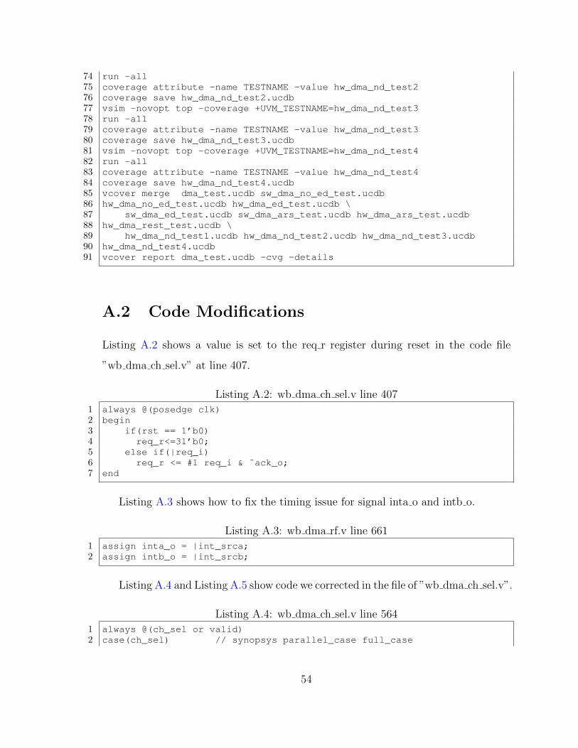
74 run -all75 coverage attribute -name TESTNAME -value hw_dma_nd_test276 coverage save hw_dma_nd_test2.ucdb77 vsim -novopt top -coverage +UVM_TESTNAME=hw_dma_nd_test378 run -all79 coverage attribute -name TESTNAME -value hw_dma_nd_test380 coverage save hw_dma_nd_test3.ucdb81 vsim -novopt top -coverage +UVM_TESTNAME=hw_dma_nd_test482 run -all83 coverage attribute -name TESTNAME -value hw_dma_nd_test484 coverage save hw_dma_nd_test4.ucdb85 vcover merge dma_test.ucdb sw_dma_no_ed_test.ucdb86 hw_dma_no_ed_test.ucdb hw_dma_ed_test.ucdb \87 sw_dma_ed_test.ucdb sw_dma_ars_test.ucdb hw_dma_ars_test.ucdb88 hw_dma_rest_test.ucdb \89 hw_dma_nd_test1.ucdb hw_dma_nd_test2.ucdb hw_dma_nd_test3.ucdb90 hw_dma_nd_test4.ucdb91 vcover report dma_test.ucdb -cvg -details
A.2 Code Modifications
Listing A.2 shows a value is set to the req r register during reset in the code file
”wb dma ch sel.v” at line 407.
Listing A.2: wb dma ch sel.v line 407
1 always @(posedge clk)2 begin3 if(rst == 1’b0)4 req_r<=31’b0;5 else if(|req_i)6 req_r <= #1 req_i & ˜ack_o;7 end
Listing A.3 shows how to fix the timing issue for signal inta o and intb o.
Listing A.3: wb dma rf.v line 661
1 assign inta_o = |int_srca;2 assign intb_o = |int_srcb;
Listing A.4 and Listing A.5 show code we corrected in the file of ”wb dma ch sel.v”.
Listing A.4: wb dma ch sel.v line 564
1 always @(ch_sel or valid)2 case(ch_sel) // synopsys parallel_case full_case
54
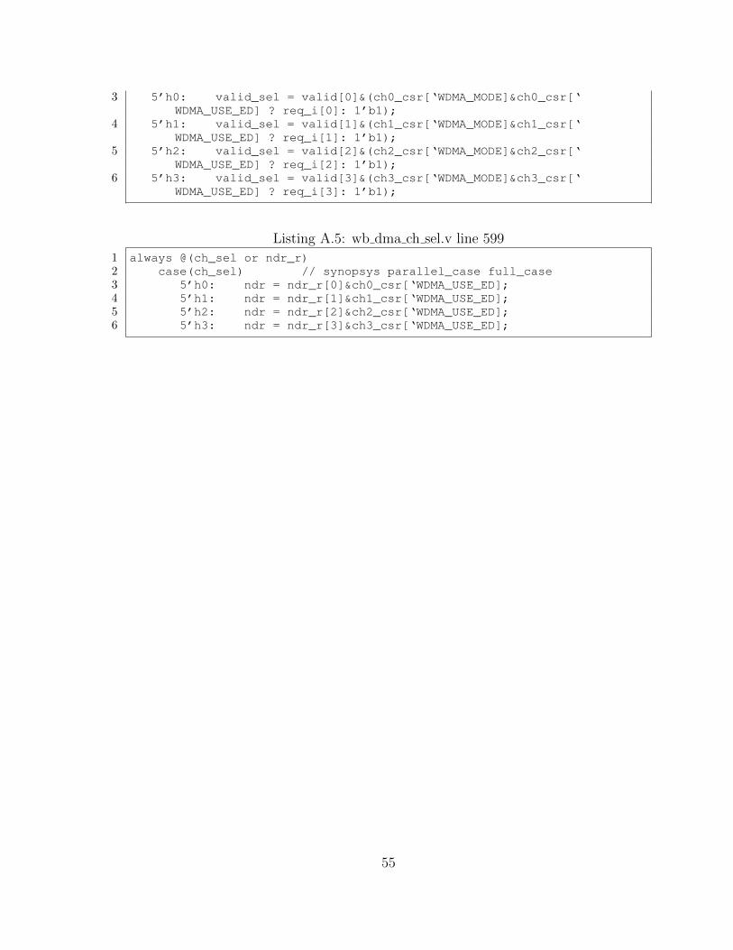
3 5’h0: valid_sel = valid[0]&(ch0_csr[‘WDMA_MODE]&ch0_csr[‘WDMA_USE_ED] ? req_i[0]: 1’b1);
4 5’h1: valid_sel = valid[1]&(ch1_csr[‘WDMA_MODE]&ch1_csr[‘WDMA_USE_ED] ? req_i[1]: 1’b1);
5 5’h2: valid_sel = valid[2]&(ch2_csr[‘WDMA_MODE]&ch2_csr[‘WDMA_USE_ED] ? req_i[2]: 1’b1);
6 5’h3: valid_sel = valid[3]&(ch3_csr[‘WDMA_MODE]&ch3_csr[‘WDMA_USE_ED] ? req_i[3]: 1’b1);
Listing A.5: wb dma ch sel.v line 599
1 always @(ch_sel or ndr_r)2 case(ch_sel) // synopsys parallel_case full_case3 5’h0: ndr = ndr_r[0]&ch0_csr[‘WDMA_USE_ED];4 5’h1: ndr = ndr_r[1]&ch1_csr[‘WDMA_USE_ED];5 5’h2: ndr = ndr_r[2]&ch2_csr[‘WDMA_USE_ED];6 5’h3: ndr = ndr_r[3]&ch3_csr[‘WDMA_USE_ED];
55
Vita
Rui Ma was born in Shaanxi Province, China. She graduated from No.1 High
School of Hu County in 2003. She obtained her Bachelor’s degree in Computer
Science and Technology and her Master’s degree in Computer System Organization
in Northwestern Polytechnical University, Xi’an, P.R. China in the year of 2007 and
2010 respectively. In 2010, she continued her study at the University of Tennessee,
Knoxville where she is expected to graduate with a Master of Science degree in
Computer Engineering in August 2016.
56