Embed Size (px)
Citation preview
MOTOROLA
SEMICONDUCTOR
DEVICE TUTORIAL
Order this document byMC68332TUT/D
MOTOROLA INC, 1995
An Introduction to the MC68332
By Sharon Darley, Mark Maiolani, and Charles Melear
1 INTRODUCTION
Use of microcontrollers (MCUs) presents new challenges as clock speeds increase and bus structures be-come more complex. In particular, designing a system with Motorola’s 32-bit MC68332 can be challengingfor those used to the 8-bit world.
The MC68332 is a member of the Motorola modular microcontroller family, a series of 16-bit and 32-bit de-vices constructed from standard on-chip peripheral modules that communicate by means of a standard in-termodule bus. The MC68332 is a sophisticated single-chip control system that incorporates a 32-bit CPUmodule (CPU32), a system integration module (SIM), a time processor unit (TPU), a queued serial module(QSM), and a 2 Kbyte standby RAM (SRAM) with TPU emulation capability. The MCU thus provides a de-signer with many options, ranging from reset configuration to interrupt generation, that must be consideredduring the design phase.
This tutorial is intended to assist development and reduce debug time for first-time designers of MC68332systems. It covers four major topics: designing the hardware, establishing communication, initializing theMCU, and troubleshooting. Each topic is discussed in a separate section that includes practical examples.
The tutorial provides a “hands-on” supplement to the
MC68332 User’s Manual
, which presents a compre-hensive overview of the MCU. For more information on device operation, electrical characteristics, registers,and control bit definition, refer to the appropriate sections of the manual. For more detailed information, referto the reference manual for each of the on-chip peripheral modules. See
6 SOURCES OF INFORMATION
for a complete list of MC68332 technical literature.
The software examples included in the tutorial, and a sample system schematic, are available through Free-ware Data Systems. The files are in the mcu332 directory in an archived file called 332init.arc. The PKXARCutility is used to de-archive these files. PKXARC itself is contained in a self-expanding file entitledPKX35A35.exe, located in the Freeware IBM directory. See
6.2 Freeware Data Systems
for a phone num-ber for modem access and addresses for internet access.
MOTOROLA MC68332TUT/D2
1 INTRODUCTION ...........................................................................................................12 DESIGNING THE HARDWARE ....................................................................................3
2.1 Using Data Bus Pins to Configure the MCU........................................................... 32.2 Choosing Memory Width ........................................................................................ 42.3 Pins that Need Pull-Up Resistors ........................................................................... 52.4 Using Sockets......................................................................................................... 62.5 Clock Circuitry......................................................................................................... 72.6 Getting Out of Reset ............................................................................................. 122.7 Power Supply........................................................................................................ 142.8 Designing for Electromagnetic Compatibility ........................................................ 152.9 Connecting Memory and Peripherals ................................................................... 182.10 Using External Interrupts .................................................................................... 22
3 ESTABLISHING COMMUNICATION .........................................................................26
3.1 Communicating with the Target Board ................................................................. 263.2 Communicating with Motorola Boards .................................................................. 28
4 SYSTEM INITIALIZATION ..........................................................................................31
4.1 Configuring the Central Processing Unit............................................................... 314.2 Configuring the System Integration Module.......................................................... 334.3 Configuring Internal RAM ..................................................................................... 374.4 Configuring the Queued Serial Module................................................................. 384.5 Configuring the Time Processor Unit.................................................................... 41
5 TROUBLESHOOTING ................................................................................................46
5.1 Critical Signals to Check....................................................................................... 465.2 Common Problems and Solutions ........................................................................ 46
6 SOURCES OF INFORMATION ..................................................................................51
6.1 Technical Literature .............................................................................................. 516.2 Freeware Data Systems ....................................................................................... 526.3 Other Sources....................................................................................................... 52
TABLE OF CONTENTS
2 DESIGNING THE HARDWARE
2.1 Using Data Bus Pins to Configure the MCU
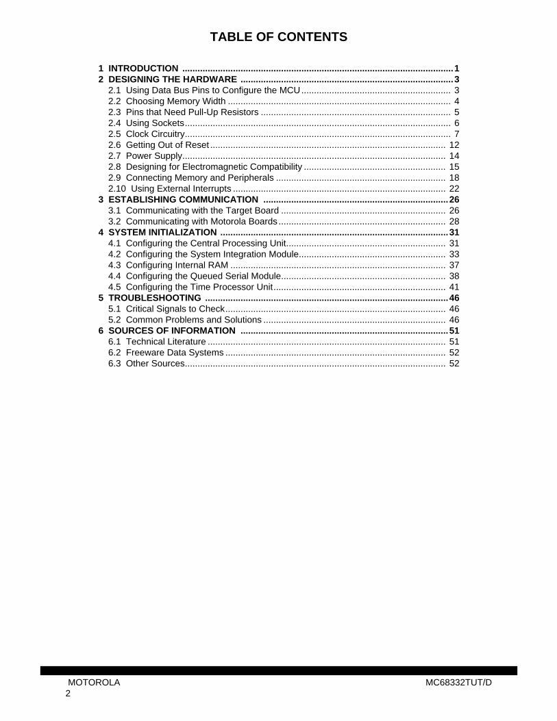
The logic level of the data bus pins during reset determines many important operating characteristics of theMCU. Ensuring that the data bus is in a known condition during reset is vital to proper operation becausethe state of each data bus pin is sampled on the rising edge of the RESET signal. The data bus pins haveweak internal pull-up circuitry that should cause them to default to a logic one if left floating (the pull-up cur-rent is 15 to 120 µA). However, since it is possible for external bus loading to overcome these internal pull-ups, it is a good idea to drive data bus pins that are critical to successful operation of the application to aknown condition during reset and for at least 5 ns afterwards (there is a 5 ns hold time requirement after therelease of RESET for a data bus pin to be recognized at a particular logic level). Table 1 shows how eachdata bus pin affects the system configuration.
As an example, Table 1 shows that the state of data bus pin 0 (DATA0) during reset determines whetherCSBOOT operates as a 16-bit chip-select or as an 8-bit chip-select. Likewise, data bus pin 1 (DATA1) de-termines whether the CS0/BR, CS1/BG, and CS2/BGACK pins function as chip-select lines or as bus con-trol signals. After reset, software can make other selections for these pins by writing to a pin assignmentregister.
A simple method of pulling a data bus pin high is to connect a 10 KΩ resistor between it and the 5 volt supply.Although putting a resistor on a data bus pin degrades performance at higher frequencies, many designersuse resistive pull-ups without significant side effects. The preferred method of driving data bus pins duringreset is by means of an active driver. A circuit to perform this function is shown in Figure 1. This circuit usesa 3-state buffer, such as a 74HC244 non-inverting octal driver, and meets the 5 ns hold time requirement.While this method does require external circuitry, it is recommended when high levels of noise may be en-countered or when high reliability of operation is an overriding concern.
Tie 74HC244 inputs high or low, respectively, so that the desired logical values will be driven to the individ-ual data bus pins when the output enable (OE) pin is driven low. The OE will be driven low when the follow-ing three conditions are met: RESET is low, data strobe (DS) is high, and read/write (R/W) is high.Conditioning RESET with R/W and DS ensures that writes to external memory will be completed before the
Notes:1. Slave mode is not a supported mode; it is used for factory testing. The slave mode must not be used in a cus-
tomer application.
Table 1 Reset Mode Selection
Mode Select Pin Default Function (Pin Left High) Alternate Function (Pin Pulled Low)
DATA0 CSBOOT is 16-bit port CSBOOT is 8-bit port
DATA1CS0CS1CS2
BRBG
BGACK
DATA2CS3CS4CS5
FC0FC1FC2
DATA3DATA4DATA5DATA6DATA7
CS6CS[7:6]CS[8:6]CS[9:6]CS[10:6]
ADDR19ADDR[20:19]ADDR[21:19]ADDR[22:19]ADDR[23:19]
DATA8 DSACK0, DSACK1, AVEC, DS, AS, SIZE PORTE I/0 pins
DATA9 IRQ[7:1], MODCLK PORTF I/0 pins
DATA11 Slave Mode Disabled1 Slave Mode Enabled1
MODCLK VC0 = System Clock EXTAL= System Clock
BKPT Background Mode Disabled Background Mode Enabled
MC68332TUT/D MOTOROLA3
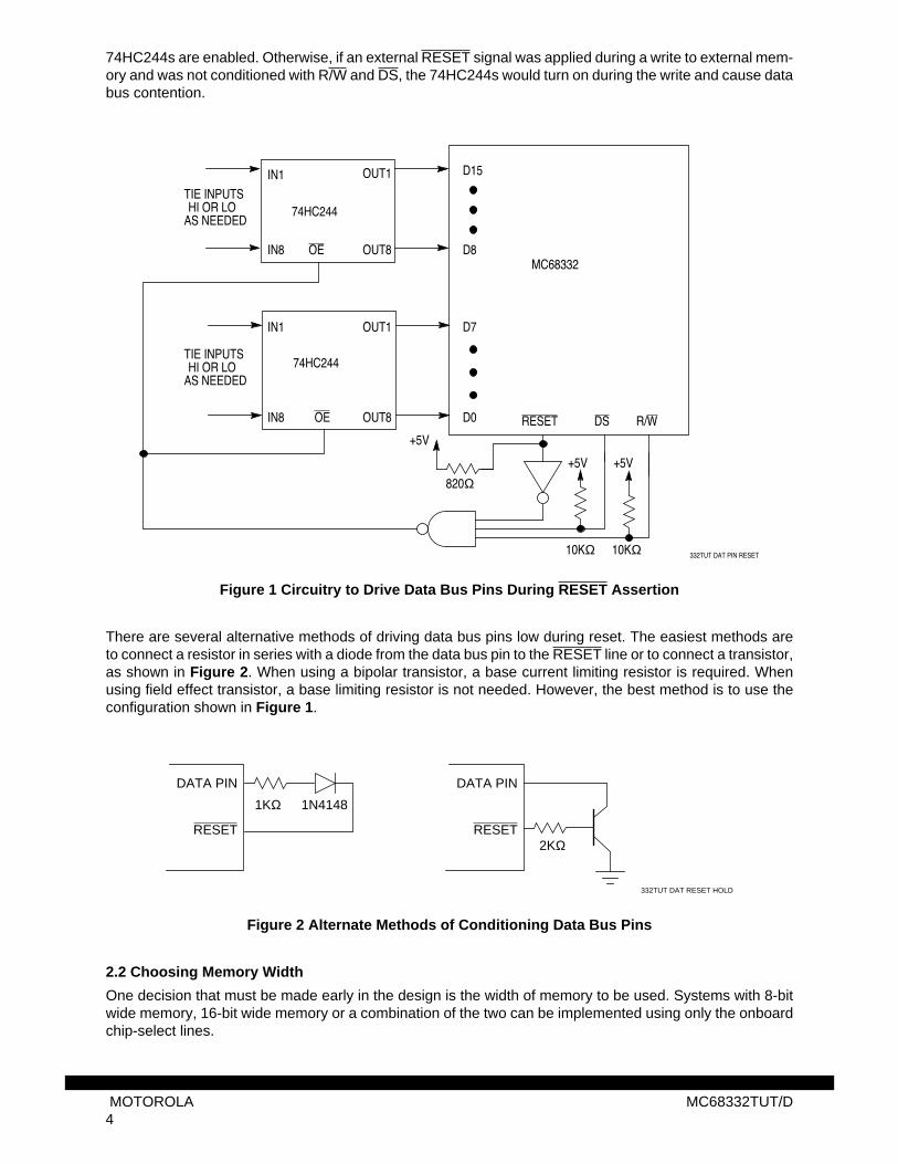
74HC244s are enabled. Otherwise, if an external RESET signal was applied during a write to external mem-ory and was not conditioned with R/W and DS, the 74HC244s would turn on during the write and cause databus contention.
Figure 1 Circuitry to Drive Data Bus Pins During RESET Assertion
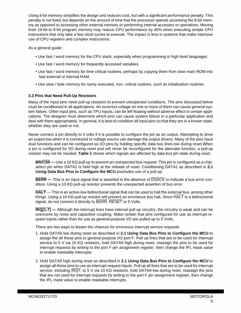
There are several alternative methods of driving data bus pins low during reset. The easiest methods areto connect a resistor in series with a diode from the data bus pin to the RESET line or to connect a transistor,as shown in Figure 2. When using a bipolar transistor, a base current limiting resistor is required. Whenusing field effect transistor, a base limiting resistor is not needed. However, the best method is to use theconfiguration shown in Figure 1.
Figure 2 Alternate Methods of Conditioning Data Bus Pins
2.2 Choosing Memory Width
One decision that must be made early in the design is the width of memory to be used. Systems with 8-bitwide memory, 16-bit wide memory or a combination of the two can be implemented using only the onboardchip-select lines.
D15
D8
D7
D0
74HC244
74HC244
RESET DS R/W
OE
OE
IN1
IN8
OUT1
OUT8
IN1
IN8
OUT1
OUT8
820Ω
10KΩ 10KΩ
+5V
+5V +5V
MC68332
332TUT DAT PIN RESET
TIE INPUTS HI OR LO
AS NEEDED
TIE INPUTS HI OR LO
AS NEEDED
332TUT DAT RESET HOLD
1KΩ 1N4148
DATA PIN
RESET2KΩ
DATA PIN
RESET
MOTOROLA MC68332TUT/D4
Using 8-bit memory simplifies the design and reduces cost, but with a significant performance penalty. Thispenalty is not fixed, but depends on the amount of time that the processor spends accessing the 8-bit mem-ory as opposed to accessing other external memory or performing internal accesses or operations. Movingfrom 16-bit to 8-bit program memory may reduce CPU performance by 40% when executing simple CPUinstructions that only take a few clock cycles to execute. The impact is less in systems that make intensiveuse of CPU registers and complex instructions.
As a general guide:
• Use fast / word memory for the CPU stack, especially when programming in high level languages.
• Use fast / word memory for frequently accessed variables.
• Use fast / word memory for time critical routines, perhaps by copying them from slow main ROM intofast external or internal RAM.
• Use slow / byte memory for rarely executed, non- critical routines, such as initialization routines.
2.3 Pins that Need Pull-Up Resistors
Many of the input pins need pull-up resistors to prevent unexpected conditions. The pins discussed belowmust be conditioned in all applications. An incorrect voltage on one or more of them can cause general sys-tem failure. Other input pins, such as TPU inputs, can be left floating without adverse effect in certain appli-cations. The designer must determine which pins can cause system failure in a particular application anddeal with them appropriately. In general, it is best to condition all input pins so that they are in a known state,whether they are used or not.
Never connect a pin directly to 5 volts if it is possible to configure the pin as an output. Attempting to drivean output low when it is connected to voltage source can damage the output drivers. Many of the pins havedual functions and can be configured as I/O pins by holding specific data bus lines low during reset.Whena pin is configured for I/O during reset and will never be reconfigured for the alternate function, a pull-upresistor may not be needed. Table 1 shows which signals are affected by data bus pin state during reset.
BR/CS0 — Use a 10 KΩ pull-up to prevent an unexpected bus request. This pin is configured as a chip-select pin when DATA1 is held high at the release of reset. Conditioning DATA1 as described in 2.1Using Data Bus Pins to Configure the MCU precludes use of a pull-up.
BERR — This is an input signal that is asserted in the absence of DSACK to indicate a bus error con-dition. Using a 10 KΩ pull-up resistor prevents the unexpected assertion of bus error.
HALT — This is an active-low bidirectional signal that can be used to halt the external bus, among otherthings. Using a 10 KΩ pull-up resistor will prevent an erroneous bus halt. Since HALT is a bidirectionalsignal, do not connect it directly to BERR, RESET or 5 Volts.
IRQ[1:7] — Although the interrupt lines have internal pull-up circuitry, the circuitry is weak and can beovercome by noise and capacitive coupling. Make certain that pins configured for use as interrupt-re-quest inputs rather than for use as general-purpose I/O are pulled up to 5 Volts.
There are two ways to lessen the chances for erroneous interrupt service requests:
1. Hold DATA9 low during reset as described in 2.1 Using Data Bus Pins to Configure the MCU toassign the all these pins to general-purpose I/O port F. Pull up lines that are to be used for interruptservice to 5 V via 10 KΩ resistors, hold DATA9 high during reset, reassign the pins to be used forinterrupt requests by writing to the port F pin assignment register, then change the IPL mask valueto enable maskable interrupts.
2. Hold DATA9 high during reset as described in 2.1 Using Data Bus Pins to Configure the MCU toassign all these pins to use as interrupt-request inputs. Pull up all lines that are to be used for interruptservice, including IRQ7, to 5 V via 10 KΩ resistors, hold DATA9 low during reset, reassign the pinsthat are not used for interrupt requests by writing to the port F pin assignment register, then changethe IPL mask value to enable maskable interrupts.
MC68332TUT/D MOTOROLA5
Remember that the level 7 interrupt is non-maskable — when configured as an interrupt line, IRQ7 isalways enabled. The only way to disable external IRQ7 interrupts is to assign the IRQ7 pin to I/O func-tion via the port F pin assignment register.
DSACK[0:1] — During bus transfers, external devices can drive these signals to indicate port width.These signals are active even if the bus transfer is to or from a peripheral that is using one of the chip-selects to terminate the bus cycle. Putting 10 KΩ pull-ups on these two pins prevents accidental asser-tion of DSACK[0:1], which can occur if the pins are left floating.
AVEC — If this signal is asserted during an interrupt acknowledge cycle, an autovector will be used forthe external interrupt being serviced. If the AVEC pin is connected permanently to ground, all externalinterrupts will autovector. Using a 10 KΩ pull-up resistor will prevent unexpected assertion of the AVECpin.
TSTME/TSC — The inactive state of this pin is 5 Volts. Pulling it low enables special test mode, but theMCU cannot enter test mode unless the state of a bit in one of the test mode registers is changed bythe software. Although this should happen only if the software is corrupted, to prevent entering specialtest mode, put a 10 KΩ pull-up resistor on this pin. Special test mode is generally used only for factorytesting, although there are certain circumstances, such as debugging TPU microcode, in which a limitedsubset of test mode capabilities are available to users. Driving this pin to approximately 1.6 times VDDcauses the MCU to place all output drivers in a high-impedance state, isolating the MCU from the restof the system.
BKPT/DSCLK — Background debug mode (BDM) operation is enabled when BKPT is asserted at therising edge of the RESET signal. BDM remains enabled until the next system reset. If BKPT is at a logiclevel one on the trailing edge of RESET, BDM is disabled. BKPT is re-latched on each rising transitionof RESET. A 4.7 KΩ pull-up resistor will ensure that BDM is not unexpectedly enabled upon reset.
R/W — Putting a 10 KΩ pull-up resistor on this pin will prevent accidental writes to memory while thedevice is being powered up. Normally, R/W is always defined. However, when power is first applied tothe device, R/W can be undefined for a few cycles. This may cause a problem for EEPROM or batterybacked up RAM.
RESET — An 820 Ω pull-up resistor is required for this pin. Do not put capacitors on the RESET pin.The reason for such a strong pull-up and no extra capacitance is that the RESET line must rise to alogic 1 within approximately10 system clocks after the MCU has driven RESET low for 512 clocks, orelse the MCU re-assert the RESET line for an additional 512 clock cycles.
MODCLK — If using the internal PLL to generate the system clock, this pin must be pulled up with a 10KΩ resistor or driven high during reset. If using an external clock source and bypassing the PLL, con-nect this pin to ground or drive it low during reset.
2.4 Using Sockets
Because of the high pin count the MCU package has a very narrow lead pitch, which makes it nearly im-possible to hand-solder onto a board. This is not a problem for design activities that can manufacture PCboards, but designers who are assembling a limited number of prototypes or who cannot manufacture PCboards will probably need to use a socket to hold the chip.The wider spacing of socket pins makes it possi-ble to connect the socket to a board.
Sockets are not a place to economize. Use a good quality socket that firmly holds the MCU in place so thatall pins maintain contact. If the MCU is likely to be removed and replaced, consider using a zero insertionforce socket.
Three socket manufacturers are:
3M — (800) 328-0411, AMP — (800) 522-6752, and Yamaichi — (408) 452-0797.
MOTOROLA MC68332TUT/D6
2.5 Clock Circuitry
The designer must decide whether to use the internal frequency synthesizer circuit or an external clock toproduce the system clock signal. Both options are discussed in the following paragraphs.
2.5.1 Using the Internal Frequency Synthesizer Circuit
The MCU uses a voltage-controlled oscillator (VCO) and a phase-locked loop (PLL) to generate an internalhigh speed clock. This arrangement permits low power operation using only the low frequency oscillator.Low frequency in CMOS technology translates into low power because power consumption is proportionalto frequency.
The internal frequency synthesizer circuit is enabled when the MODCLK pin is pulled high during reset. Thesynthesizer requires a reference frequency in order to operate. There are two reference frequency options:using a crystal oscillator circuit or using an external clock reference, such as a canned oscillator circuit (asingle package which contains the crystal and buffer circuit) as the input.
2.5.2 Using a Crystal Oscillator Circuit
2.5.2.1 Oscillator Components
The crystal oscillator used is a Pierce oscillator, also known as a parallel resonant crystal oscillator. It isshown in Figure 3. Its components consist of a series resistor, a feedback resistor, a crystal, an inverter,and two capacitors:
Rs — Series resistor Rs must be large enough to appropriately limit current to the crystal and yet smallenough to provide enough current to start it oscillating quickly. The smaller Rs, the faster the oscillatorwill start. However, if Rs is too small, the crystal will start up in unpredictable modes or dissipate toomuch power. This can cause heating problems. In extreme cases, the crystal may even be damagedand not work properly again. If Rs is too large, the oscillator will start very slowly or not at all. The bestway to minimize start-up time is to minimize the size of Rs within the guidelines of the maximum powerdissipation.
The crystal manufacturer generally recommends a range of values to use. To ensure that Rs is largeenough to prevent the crystal from being overdriven, observe the output frequency as a function of VDDon the CLKOUT pin. If the crystal is overdriven at start-up, the frequency will be very unstable.
Rf — Feedback resistor Rf is used to bias the inverter between EXTAL and XTAL inside the MCU. Rfaffects the loop gain; lower values reduce gain, while higher values increase gain.
C1 and C2 — The series combination of C1 and C2 provides the parallel load for the crystal. Their val-ues may be varied to trim frequency. In high frequency applications, C1 and C2 are usually equal. How-ever, in low frequency applications, C1 can be smaller than C2 (about 5 pF) to provide a higher voltageat the EXTAL input. A wider voltage swing at this input will result in lower power-supply current. Usually,the actual capacitances will be smaller than the intended capacitances since circuit and layout capaci-tances add to the values of C1 and C2.
Inverter — The inverter is inside the MCU. It provides the 180 degree phase shift necessary for oscil-lation.
Crystal — The crystal is made of piezoelectric quartz. It must be a good quality crystal that is capableof suppressing harmonics and overtones and quickly locking onto the fundamental frequency. If a par-ticular crystal type or brand is prone to starting with overtones or harmonics, don’t use it. No amount ofcircuit design can compensate for a bad or poor quality crystal.
The MCU is designed to use a 32.768 kHz AT-cut crystal to produce an 8.389 MHz CLKOUT signal. Thefrequency of the internal clock can be increased or decreased by writing to the SYNCR register. Figure 3shows clock circuitry for a Daishinku DMX-38 32.768 KHz crystal, but the circuit will work for most other32.768 kHz crystals also. To use other crystal values (the allowable range is 20 kHz - 50 kHz), consult thecrystal vendor for analysis of the crystal components needed.
MC68332TUT/D MOTOROLA7
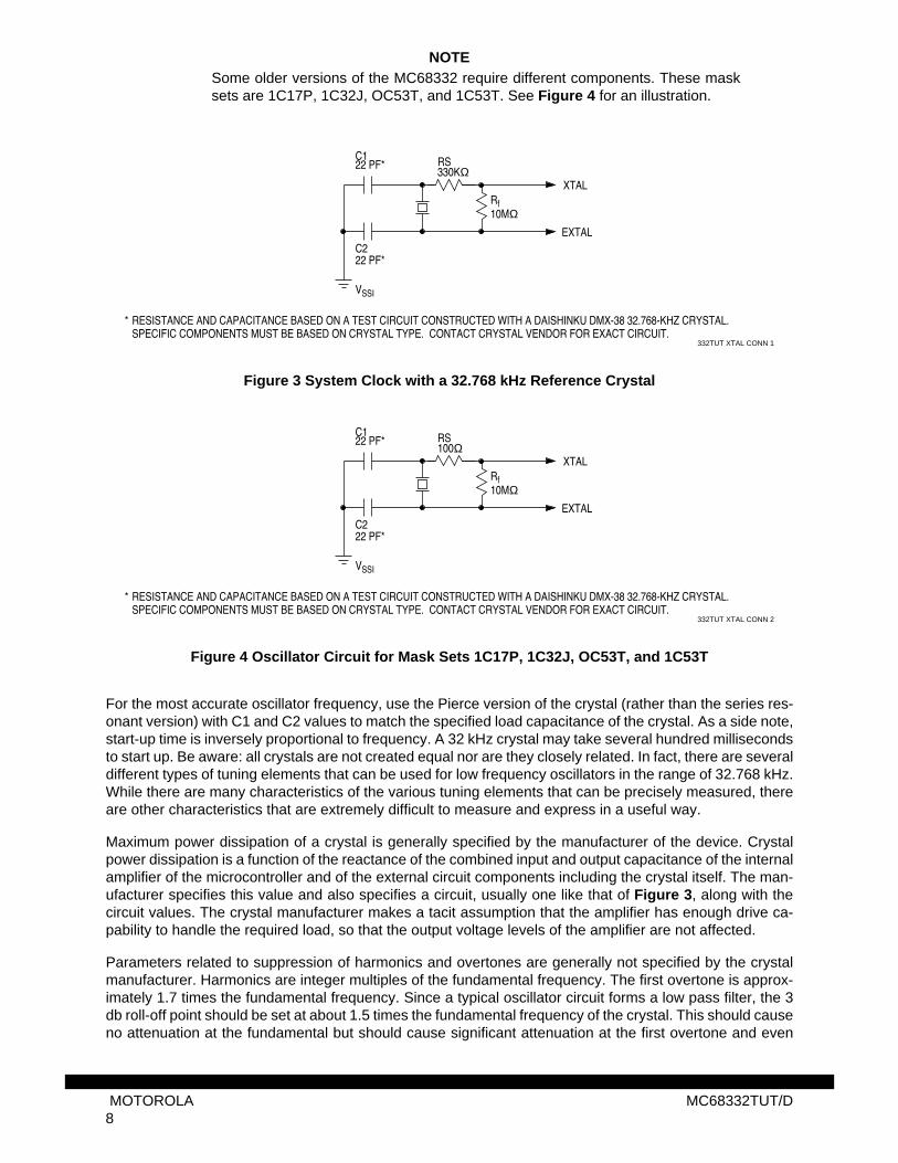
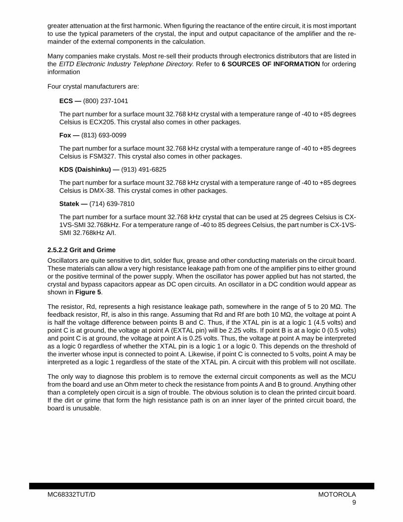
NOTESome older versions of the MC68332 require different components. These masksets are 1C17P, 1C32J, OC53T, and 1C53T. See Figure 4 for an illustration.
Figure 3 System Clock with a 32.768 kHz Reference Crystal
Figure 4 Oscillator Circuit for Mask Sets 1C17P, 1C32J, OC53T, and 1C53T
For the most accurate oscillator frequency, use the Pierce version of the crystal (rather than the series res-onant version) with C1 and C2 values to match the specified load capacitance of the crystal. As a side note,start-up time is inversely proportional to frequency. A 32 kHz crystal may take several hundred millisecondsto start up. Be aware: all crystals are not created equal nor are they closely related. In fact, there are severaldifferent types of tuning elements that can be used for low frequency oscillators in the range of 32.768 kHz.While there are many characteristics of the various tuning elements that can be precisely measured, thereare other characteristics that are extremely difficult to measure and express in a useful way.
Maximum power dissipation of a crystal is generally specified by the manufacturer of the device. Crystalpower dissipation is a function of the reactance of the combined input and output capacitance of the internalamplifier of the microcontroller and of the external circuit components including the crystal itself. The man-ufacturer specifies this value and also specifies a circuit, usually one like that of Figure 3, along with thecircuit values. The crystal manufacturer makes a tacit assumption that the amplifier has enough drive ca-pability to handle the required load, so that the output voltage levels of the amplifier are not affected.
Parameters related to suppression of harmonics and overtones are generally not specified by the crystalmanufacturer. Harmonics are integer multiples of the fundamental frequency. The first overtone is approx-imately 1.7 times the fundamental frequency. Since a typical oscillator circuit forms a low pass filter, the 3db roll-off point should be set at about 1.5 times the fundamental frequency of the crystal. This should causeno attenuation at the fundamental but should cause significant attenuation at the first overtone and even
332TUT XTAL CONN 1
EXTAL
XTAL
10MΩ
330KΩ
22 PF*
22 PF*
VSSI
RESISTANCE AND CAPACITANCE BASED ON A TEST CIRCUIT CONSTRUCTED WITH A DAISHINKU DMX-38 32.768-KHZ CRYSTAL.SPECIFIC COMPONENTS MUST BE BASED ON CRYSTAL TYPE. CONTACT CRYSTAL VENDOR FOR EXACT CIRCUIT.
*
RSC1
C2
Rf
332TUT XTAL CONN 2
EXTAL
XTAL
10MΩ
100Ω
22 PF*
22 PF*
VSSI
RESISTANCE AND CAPACITANCE BASED ON A TEST CIRCUIT CONSTRUCTED WITH A DAISHINKU DMX-38 32.768-KHZ CRYSTAL.SPECIFIC COMPONENTS MUST BE BASED ON CRYSTAL TYPE. CONTACT CRYSTAL VENDOR FOR EXACT CIRCUIT.
*
RSC1
C2
Rf
MOTOROLA MC68332TUT/D8
greater attenuation at the first harmonic. When figuring the reactance of the entire circuit, it is most importantto use the typical parameters of the crystal, the input and output capacitance of the amplifier and the re-mainder of the external components in the calculation.
Many companies make crystals. Most re-sell their products through electronics distributors that are listed inthe EITD Electronic Industry Telephone Directory. Refer to 6 SOURCES OF INFORMATION for orderinginformation
Four crystal manufacturers are:
ECS — (800) 237-1041
The part number for a surface mount 32.768 kHz crystal with a temperature range of -40 to +85 degreesCelsius is ECX205. This crystal also comes in other packages.
Fox — (813) 693-0099
The part number for a surface mount 32.768 kHz crystal with a temperature range of -40 to +85 degreesCelsius is FSM327. This crystal also comes in other packages.
KDS (Daishinku) — (913) 491-6825
The part number for a surface mount 32.768 kHz crystal with a temperature range of -40 to +85 degreesCelsius is DMX-38. This crystal comes in other packages.
Statek — (714) 639-7810
The part number for a surface mount 32.768 kHz crystal that can be used at 25 degrees Celsius is CX-1VS-SMI 32.768kHz. For a temperature range of -40 to 85 degrees Celsius, the part number is CX-1VS-SMI 32.768kHz A/I.
2.5.2.2 Grit and Grime
Oscillators are quite sensitive to dirt, solder flux, grease and other conducting materials on the circuit board.These materials can allow a very high resistance leakage path from one of the amplifier pins to either groundor the positive terminal of the power supply. When the oscillator has power applied but has not started, thecrystal and bypass capacitors appear as DC open circuits. An oscillator in a DC condition would appear asshown in Figure 5.
The resistor, Rd, represents a high resistance leakage path, somewhere in the range of 5 to 20 MΩ. Thefeedback resistor, Rf, is also in this range. Assuming that Rd and Rf are both 10 MΩ, the voltage at point Ais half the voltage difference between points B and C. Thus, if the XTAL pin is at a logic 1 (4.5 volts) andpoint C is at ground, the voltage at point A (EXTAL pin) will be 2.25 volts. If point B is at a logic 0 (0.5 volts)and point C is at ground, the voltage at point A is 0.25 volts. Thus, the voltage at point A may be interpretedas a logic 0 regardless of whether the XTAL pin is a logic 1 or a logic 0. This depends on the threshold ofthe inverter whose input is connected to point A. Likewise, if point C is connected to 5 volts, point A may beinterpreted as a logic 1 regardless of the state of the XTAL pin. A circuit with this problem will not oscillate.
The only way to diagnose this problem is to remove the external circuit components as well as the MCUfrom the board and use an Ohm meter to check the resistance from points A and B to ground. Anything otherthan a completely open circuit is a sign of trouble. The obvious solution is to clean the printed circuit board.If the dirt or grime that form the high resistance path is on an inner layer of the printed circuit board, theboard is unusable.
MC68332TUT/D MOTOROLA9
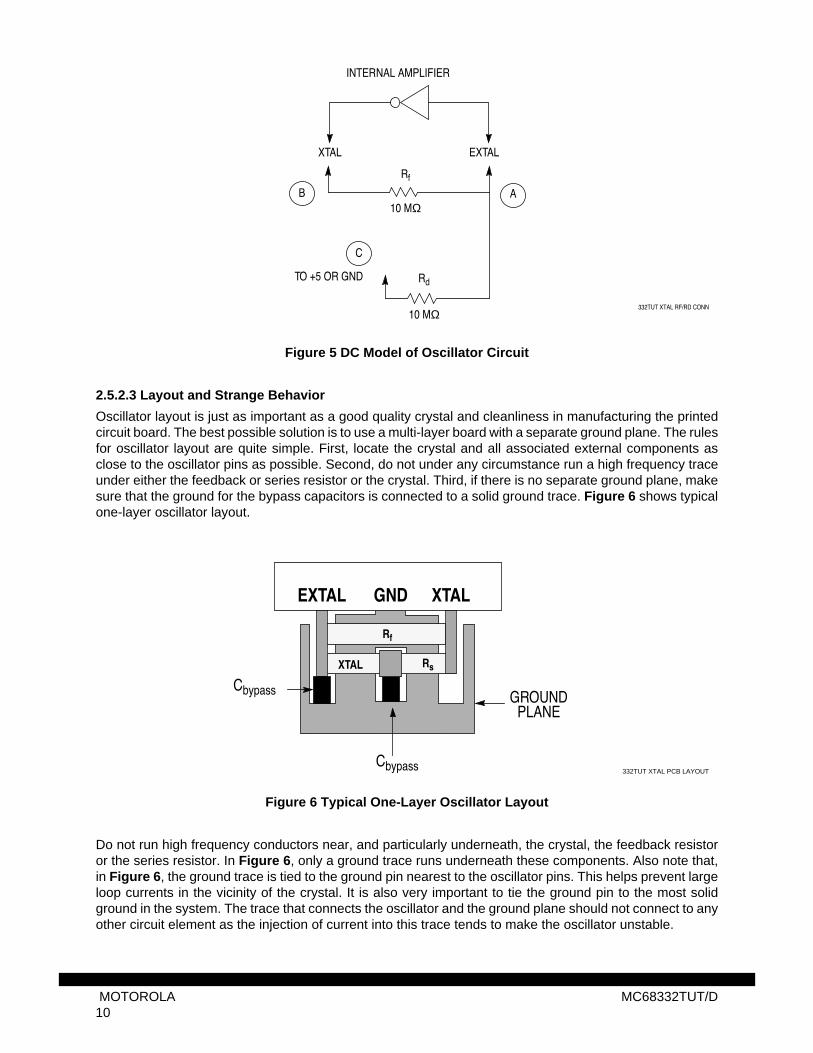
Figure 5 DC Model of Oscillator Circuit
2.5.2.3 Layout and Strange Behavior
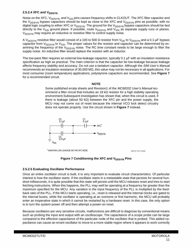
Oscillator layout is just as important as a good quality crystal and cleanliness in manufacturing the printedcircuit board. The best possible solution is to use a multi-layer board with a separate ground plane. The rulesfor oscillator layout are quite simple. First, locate the crystal and all associated external components asclose to the oscillator pins as possible. Second, do not under any circumstance run a high frequency traceunder either the feedback or series resistor or the crystal. Third, if there is no separate ground plane, makesure that the ground for the bypass capacitors is connected to a solid ground trace. Figure 6 shows typicalone-layer oscillator layout.
Figure 6 Typical One-Layer Oscillator Layout
Do not run high frequency conductors near, and particularly underneath, the crystal, the feedback resistoror the series resistor. In Figure 6, only a ground trace runs underneath these components. Also note that,in Figure 6, the ground trace is tied to the ground pin nearest to the oscillator pins. This helps prevent largeloop currents in the vicinity of the crystal. It is also very important to tie the ground pin to the most solidground in the system. The trace that connects the oscillator and the ground plane should not connect to anyother circuit element as the injection of current into this trace tends to make the oscillator unstable.
332TUT XTAL RF/RD CONN
XTAL EXTAL
Rf
TO +5 OR GND Rd
AB
C
INTERNAL AMPLIFIER
10 MΩ
10 MΩ
332TUT XTAL PCB LAYOUT
XTAL Rs
Cbypass
Cbypass
GROUNDPLANE
Rf
EXTAL GND XTAL
MOTOROLA MC68332TUT/D10
2.5.2.4 XFC and VDDSYN
Noise on the XFC, VDDSYN, and VSSI pins causes frequency shifts in CLKOUT. The XFC filter capacitor andthe VDDSYN bypass capacitors should be kept as close to the XFC and VDDSYN pins as possible, with nodigital logic coupling to either XFC or VDDSYN. The ground for the VDDSYN bypass capacitors should be tieddirectly to the VSSI ground plane. If possible, route VDDSYN and VSSI as separate supply runs or planes.VDDSYN may require an inductive or resistive filter to control supply noise.
A VDDSYN resistive filter would consist of a 100 to 500 Ω resistor from VDD to VDDSYN and a 0.1-µF bypasscapacitor from VDDSYN to VSSI. The proper values for the resistor and capacitor can be determined by ex-amining the frequency of the VDDSYN noise. The RC time constant needs to be large enough to filter thesupply noise. An inductive filter would replace the resistor with an inductor.
The low-pass filter requires an external low-leakage capacitor, typically 0.1 µF with an insulation resistancespecification as high as practical. The main criterion is that the capacitor be low-leakage because leakageaffects frequency stability and accuracy. Do not use a tantalum capacitor. Although the SIM User’s Manualrecommends an insulation resistance of 30,000 MΩ, this value may not be necessary in all applications. Formost consumer (room temperature) applications, polystyrene capacitors are recommended. See Figure 7for a recommended circuit.
NOTESome published errata sheets and Revision1 of the MC68332 User’s Manual rec-ommend a filter circuit that includes an 18 kΩ resistor for a high stability operatingenvironment.Subsequent investigation has shown that, when this circuit is used, ifthere is leakage (about 50 kΩ) between the XFC pin and the power supply, theMCU may not come out of reset because the internal VCO lock detect circuitrydoes not operate properly. Use the circuit shown in Figure 7 instead.
Figure 7 Conditioning the XFC and VDDSYN Pins
2.5.2.5 Evaluating Oscillator Performance
Once an entire oscillator circuit is built, it is very important to evaluate circuit characteristics. Of particularinterest is how the oscillator starts. If the oscillator starts in a metastable state that persists for several hun-dred milliseconds, it is quite possible that this state will persist until the MCU releases reset and tries to startfetching instructions. When this happens, the PLL may well be operating at a frequency far greater than themaximum specified for the MCU. Any variation in the input frequency of the PLL is multiplied by the feed-back ratio of the PLL. If the MCU starts operating, i.e., reset is released and the internal clocks are gated tothe internal buses, while the oscillator is operating at an overtone or first harmonic, the MCU will probablyenter an inoperative state in which it cannot be restarted by a hardware reset. In this case, the only optionis to turn the system power off and then attempt a power-on reset.
Because oscillators are very sensitive circuits, malfunctions are difficult to diagnose by conventional meanssuch as probing the input and output with an oscilloscope. The capacitance of a scope probe can be largecompared to the effective capacitance of the particular node of the oscillator that is probed. This added ca-pacitance can cause an errant oscillator to move to a more stable region where it appears to work correctly
332TUT XFC CONN* MAINTAIN LOW LEAKAGE ON THE XFC NODE.
VDDSYN
0.01µF
0.1µF
XFC*
VSSI
0.1µF
C4
C3 C1
MC68332TUT/D MOTOROLA11
or, on the other hand, a working oscillator could be moved into a region of no oscillation at all. Therefore, itis important to measure oscillator performance indirectly. This can be done through the CLKOUT pin, whichis a buffered form of the internal system clock. Monitoring the CLKOUT pin with an oscilloscope does notaffect the oscillator and provides an accurate representation of oscillator problems. If the MCU is runningoff the internal PLL and a 32.768 kHz crystal, the CLKOUT frequency should be 8.389 MHz.
The CLKOUT signal is likely to do one of three things when power is turned on. It will either remain at aconstant DC level, jump quickly to the proper frequency, or, first jump to the desired frequency, then entera very high frequency metastable state and then jump back to the fundamental frequency. With a smallamount of practice, these metastable states, which last for approximately 100 to 500 ms, can be easily de-tected on an oscilloscope. In the third case, the MCU generally takes almost a second to reach steady state,which provides plenty of time for it to attempt operation while the clock is in a metastable state.
2.5.2.6 Using a Canned Oscillator
A second option when using the internal frequency synthesizer circuit is to hold MODCLK high during resetand connect an external clock reference or canned oscillator (a single package that includes the oscillatorand required external components) to the EXTAL pin. Leave the XTAL pin floating, but connect the filtercircuit shown in Figure 7 to VDDSYN and XFC. The allowable frequency range is 20-50 kHz.
One manufacturer of canned oscillators is:
Oak Frequency Control Group — (717) 486-3411
2.5.3 Using an External Clock
To use an external clock, connect a clock signal to the EXTAL pin and hold MODCLK low during reset.Leave the XTAL and XFC pins floating, but connect VDDSYN to power. The frequency control bits in theSYNCR register have no effect; the signal applied to the EXTAL pin should appear unchanged on the CLK-OUT line. The external clock must comply with the following expression.
Minimum external clock high/low time is a specification given in the device electrical characteristics.
2.6 Getting Out of Reset
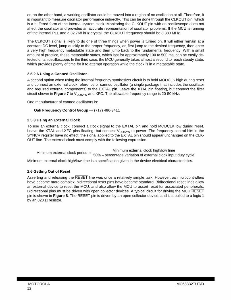
Asserting and releasing the RESET line was once a relatively simple task. However, as microcontrollershave become more complex, bidirectional reset pins have become standard. Bidirectional reset lines allowan external device to reset the MCU, and also allow the MCU to assert reset for associated peripherals.Bidirectional pins must be driven with open collector devices. A typical circuit for driving the MCU RESETpin is shown in Figure 8. The RESET pin is driven by an open collector device, and it is pulled to a logic 1by an 820 Ω resistor.
Minimum external clock periodMinimum external clock high/low time
50% percentage variation of external clock input duty cycle–----------------------------------------------------------------------------------------------------------------------------------------------------------------=
MOTOROLA MC68332TUT/D12
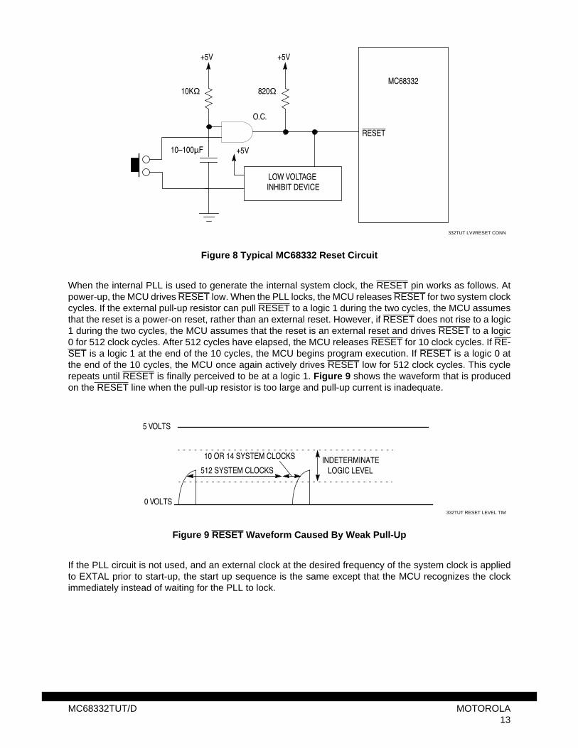
Figure 8 Typical MC68332 Reset Circuit
When the internal PLL is used to generate the internal system clock, the RESET pin works as follows. Atpower-up, the MCU drives RESET low. When the PLL locks, the MCU releases RESET for two system clockcycles. If the external pull-up resistor can pull RESET to a logic 1 during the two cycles, the MCU assumesthat the reset is a power-on reset, rather than an external reset. However, if RESET does not rise to a logic1 during the two cycles, the MCU assumes that the reset is an external reset and drives RESET to a logic0 for 512 clock cycles. After 512 cycles have elapsed, the MCU releases RESET for 10 clock cycles. If RE-SET is a logic 1 at the end of the 10 cycles, the MCU begins program execution. If RESET is a logic 0 atthe end of the 10 cycles, the MCU once again actively drives RESET low for 512 clock cycles. This cyclerepeats until RESET is finally perceived to be at a logic 1. Figure 9 shows the waveform that is producedon the RESET line when the pull-up resistor is too large and pull-up current is inadequate.
Figure 9 RESET Waveform Caused By Weak Pull-Up
If the PLL circuit is not used, and an external clock at the desired frequency of the system clock is appliedto EXTAL prior to start-up, the start up sequence is the same except that the MCU recognizes the clockimmediately instead of waiting for the PLL to lock.
332TUT LVI/RESET CONN
RESET
O.C.
MC68332
LOW VOLTAGEINHIBIT DEVICE
+5V
10KΩ 820Ω
10–100µF
+5V +5V
332TUT RESET LEVEL TIM
0 VOLTS
5 VOLTS
INDETERMINATELOGIC LEVEL512 SYSTEM CLOCKS
10 OR 14 SYSTEM CLOCKS
MC68332TUT/D MOTOROLA13

2.7 Power Supply
Always connect all power and ground pins to power sources. Since internal power buses only serve about8 - 10 pins each, the power and ground pins are usually not connected together within the device. If anypower pin is left floating, the pins served by the floating power pin can receive power from internal circuitrysuch as internal protection diodes. However, the current path will usually have several diode drops, resultingin a low output high voltage (about 3 volts) on associated output pins.
2.7.1 Low Voltage Inhibit Devices
A low voltage inhibit (LVI) device (also referred to as a reset supervisor circuit) protects the MCU by keepingit in reset until full voltage is applied and by forcing an external reset as soon as power starts to fall. Thisprevents the MCU from going into an indeterminate state due to a power supply failure or slow power supplyramp-up time.
A number of manufacturers make LVI devices that can be used with the MCU.
Analog Devices — (617) 461-3392
LVI part numbers are ADM698 and ADM699. These devices require pull-up resistors.
Dallas Semiconductor— (214) 450-0448
Various reset supervisor circuits. Part numbers DS1233A, D, and M do not require pull-up resistors.
Linear Technologies— (408) 432-1900
LVI part numbers are LTC692 and LTC693. These devices require a pull-up resistor.
Maxim — (800) 998-8800 or (408) 737-7600
Various reset supervisor circuits. MAX 690 and MAX 700 series devices require pull-up resistors, butMAX 809 devices do not.
Motorola, Inc.— (408) 432-1900
Reset supervisor circuit part number is MC34064. It requires an external pull-up resistor.
2.7.1.1 Using LVI Devices with External Oscillators
An LVI device provides an extra degree of protection when an external oscillator that has an independentpower supply is used to generate the system clock. In this case, the LVI device ensures that the oscillatordoes not power up before the MCU.
2.7.1.2 Using LVI Devices with Multiple Power Supplies
Take special precautions when system components that are connected to each other have separate powersupplies. Generally, one power supply will reach operating voltage more quickly than another. A device con-nected to this fast supply can begin to operate before devices connected to a slower supply have reachedoperating voltage. If a device connected to a fast supply drives logic one levels to a device connected to aslow supply, the input protection diodes of the slow -starting device can be momentarily forward biased, andsignificant current can be injected into the device substrate. In the case of an MCU, the injected current cancause internal nodes to be improperly charged or discharged. Since this action is random, it is impossibleto predict what will happen when injection occurs. Usually, the processor will fail to fetch opcodes. Figure10 shows how to use LVI devices to prevent this problem. Each power supply is monitored by a separateLVI device. Signals from other boards are inhibited until correct operating voltage is applied.
MOTOROLA MC68332TUT/D14
Figure 10 Using LVI Devices with Multiple Power Supplies
2.8 Designing for Electromagnetic Compatibility
Because of the fast clock speed and relatively short rise and fall times of MCU signals, the designer mustconsider electromagnetic compatibility (EMC) issues. All high-speed digital devices radiate noise, and ifFCC compliance is required, the designer must do everything possible to limit emissions from the MCU. Useof a four-layer board is probably the best single option the designer has. Although a two-layer board willwork, a multilayer PCB is much more effective at both protecting the MCU from emissions, and reducingemissions from the MCU. EMC compatibility is a complex topic, and this tutorial can present only a briefoverview of EMC design techniques.
2.8.1 Reducing Power Supply Noise
The MCU is very susceptible to noise created by large or rapid fluctuations in current through a particularpower supply pin. The power supply pins are divided up into VDDE/VSSE and VDDI/VSSI. The VDDE/VSSE pinspower the external drivers and pins, while the VDDI/VSSI pins power the internal peripherals and core of theMCU. It is very important to keep the VDDI/VSSI pins free of noise as the CPU is generally more sensitive topower supply noise than the port drivers. When designing a multilayer board, simply route the power andground pins directly to the power and ground planes; when designing a two-layer board, however, it is bestto isolate the power bus that serves the core of the chip from the power bus that serves the port drivers.
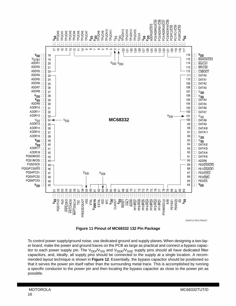
Figure 11 shows groups of pins that are powered by the same supply pins. Although only the 132- pin plas-tic surface mount package is shown, the groups for the144-pin package are the same. In each group, theVDDE and VSSE pins that power a particular group are shown in bold face type. The VDDI and VSSI pins arelabeled as such. EXTAL, XTAL, and XFC are powered only by VDDSYN.
When control of noise on the power buses is important, it is possible to isolate sections of the chip that areparticularly noisy. The data and address buses are particularly noisy because they continually change state,and the same can be true of serial ports and timer pins. The amount of noise generated by a particular pinis dependent upon the load being driven and the switching frequency. A designer who knows which powerand ground connections serve particular pins can shield other signal conductors from these noisy lines.
332TUT DUAL RESET CONN
POWER SUPPLY POWER SUPPLY
LOWVOLTAGEINHIBIT
DEVICE A DEVICE B
LOWVOLTAGEINHIBIT
MC68332TUT/D MOTOROLA15
PQ 10
Figure 11 Pinout of MC68332 132 Pin Package
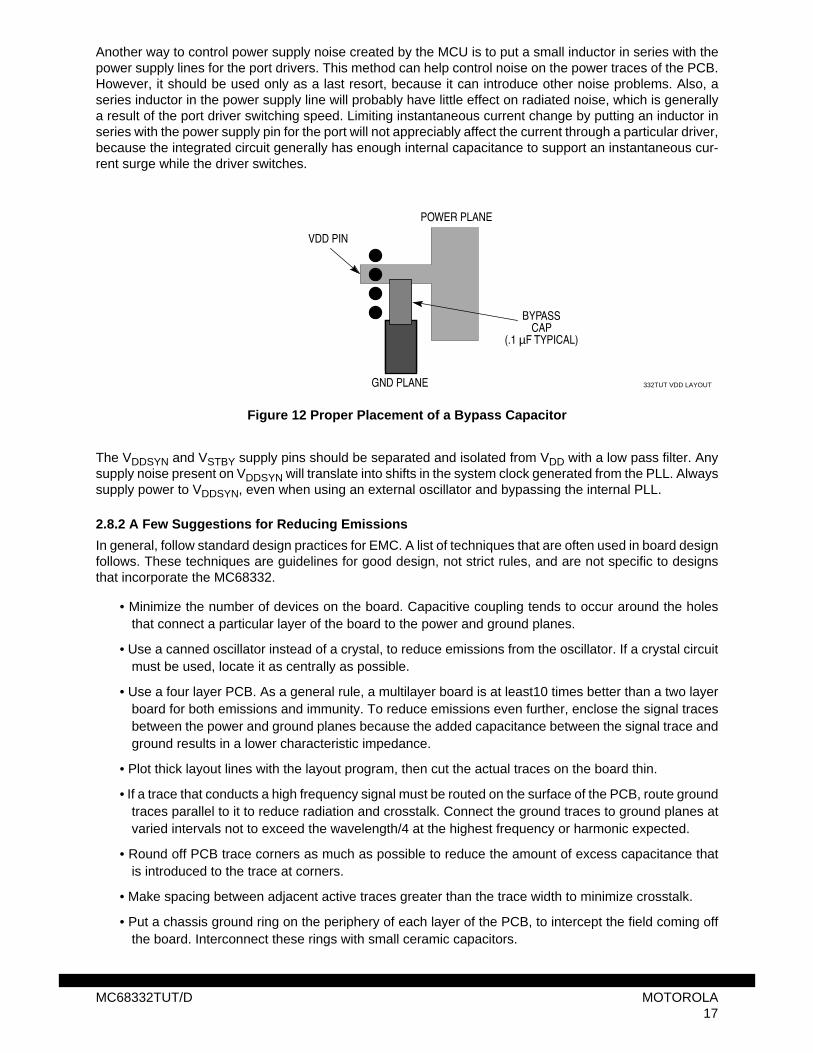
To control power supply/ground noise, use dedicated ground and supply planes. When designing a two-lay-er board, make the power and ground traces on the PCB as large as practical and connect a bypass capac-itor to each power supply pin. The VDDI/VSSI and VDDE/VSSE supply pins should all have dedicated filtercapacitors, and, ideally, all supply pins should be connected to the supply at a single location. A recom-mended layout technique is shown in Figure 12. Essentially, the bypass capacitor should be positioned sothat it serves the power pin itself rather than the surrounding metal trace. This is accomplished by runninga specific conductor to the power pin and then locating the bypass capacitor as close to the power pin aspossible.
MC68332
1851
17 11716 15 14 13 12 11 10 9 8 7 6 5 4 3
131
130
129
128
127
126
125
124
123
122
121
120
119
118
52 53 54 55 56 57 58 59 60 61 62 63 64 65 66 67 68 69 70 71 72 73 74 75 76 77 78 79 80 81 82 83
1920212223242526272829303132333435363738394041424344454647484950
11611511411311211111010910810710610510410310210110099989796959493929190898887868584
DATA9DATA10DATA11
DATA12DATA13DATA14DATA15ADDR0
PQS7
/TxD
RxD
IPIP
E/DS
O
FREE
ZE/Q
UO
T
XTAL
EXT
AL
XFC
CLK
OU
T
PF0/
MO
DCLK
PE7/
SIZ1
PE6/
SIZ
0
ADDR1ADDR2ADDR3ADDR4ADDR5ADDR6ADDR7ADDR8
ADDR9ADDR10ADDR11ADDR12
ADDR13ADDR14ADDR15ADDR16
ADDR17ADDR18
PQS0/MISOPQS1/MOSIPQS2/SCK
S3/PCS0/SSPQS4/PCS1PQS5/PCS2PQS6/PCS3
TPU
CH0
TPUC
H1
TPU
CH2
TPUC
H3
TPUC
H4TP
UCH
5TP
UCH
6TP
UCH
7
TPU
CH8
TPUC
H9
TPU
CH10
TPUC
H11
TPUC
H13
TPU
CH14
TPUC
H15
T2C
LK
TPU
CH12
DATA0DATA1DATA2DATA3
DATA4DATA5DATA6DATA7
DATA8
V SS V SS
V SS VDD V SS
VD
D
V SS
VD
D
VDD
VDDVSS
VSS
VDDVSS
VDD
V SS VSS
VDD
V SS
VDDVSS
VDD
VDD
VDDVSS
VSS
PE1/DSACKPE0/DSACK
PE2/AVECPE3/RMCPE5/DS
CSBOOT
BGACK/CS2BG/CS1BR/CS0
PC0/
FC0/
CS3
PC1/
FC1/
CS4
PC2/
FC2/
CS5
PC
3/AD
DR
19/C
S6PC
4/AD
DR20
/CS7
PC
5/AD
DR
21/C
S8PC
6/AD
DR22
/CS9
ADD
R23
/CS1
0
ASR/W
PF1/
IRQ
1PF
2/IR
Q2
PF3/
IRQ
3PF
4/IR
Q4
PF5/
IRQ
5PF
6/IR
Q6
PF7/
IRQ
7B
ERR
HAL
TR
ESET
TSC
BKPT
/DSC
LKIF
ETCH
/DSI
2 113
2
VSTBY
VDD
SYN VDD V SS
VSSI VDDI
VSSI
VSSI VDDI
VSSI
33332TUT MCU PINOUT
MOTOROLA MC68332TUT/D16
Another way to control power supply noise created by the MCU is to put a small inductor in series with thepower supply lines for the port drivers. This method can help control noise on the power traces of the PCB.However, it should be used only as a last resort, because it can introduce other noise problems. Also, aseries inductor in the power supply line will probably have little effect on radiated noise, which is generallya result of the port driver switching speed. Limiting instantaneous current change by putting an inductor inseries with the power supply pin for the port will not appreciably affect the current through a particular driver,because the integrated circuit generally has enough internal capacitance to support an instantaneous cur-rent surge while the driver switches.
Figure 12 Proper Placement of a Bypass Capacitor
The VDDSYN and VSTBY supply pins should be separated and isolated from VDD with a low pass filter. Anysupply noise present on VDDSYN will translate into shifts in the system clock generated from the PLL. Alwayssupply power to VDDSYN, even when using an external oscillator and bypassing the internal PLL.
2.8.2 A Few Suggestions for Reducing Emissions
In general, follow standard design practices for EMC. A list of techniques that are often used in board designfollows. These techniques are guidelines for good design, not strict rules, and are not specific to designsthat incorporate the MC68332.
• Minimize the number of devices on the board. Capacitive coupling tends to occur around the holesthat connect a particular layer of the board to the power and ground planes.
• Use a canned oscillator instead of a crystal, to reduce emissions from the oscillator. If a crystal circuitmust be used, locate it as centrally as possible.
• Use a four layer PCB. As a general rule, a multilayer board is at least10 times better than a two layerboard for both emissions and immunity. To reduce emissions even further, enclose the signal tracesbetween the power and ground planes because the added capacitance between the signal trace andground results in a lower characteristic impedance.
• Plot thick layout lines with the layout program, then cut the actual traces on the board thin.
• If a trace that conducts a high frequency signal must be routed on the surface of the PCB, route groundtraces parallel to it to reduce radiation and crosstalk. Connect the ground traces to ground planes atvaried intervals not to exceed the wavelength/4 at the highest frequency or harmonic expected.
• Round off PCB trace corners as much as possible to reduce the amount of excess capacitance thatis introduced to the trace at corners.
• Make spacing between adjacent active traces greater than the trace width to minimize crosstalk.
• Put a chassis ground ring on the periphery of each layer of the PCB, to intercept the field coming offthe board. Interconnect these rings with small ceramic capacitors.
332TUT VDD LAYOUTGND PLANE
POWER PLANE
BYPASSCAP
VDD PIN
(.1 µF TYPICAL)
MC68332TUT/D MOTOROLA17
• Use ferrite chokes when troubleshooting. Placing a choke around a signal line and the return conduc-tor carrying a differential signal causes fields developed in the ferrite core by the opposing currentsto cancel. Ferrite chokes can also be used on input/output lines. Because board-mounted chokes in-crease the number of holes connecting to the supply planes, they should be used only as a last resort.
• Localize any high frequency circuits, such as the clock and address or data buses. Decouple locallyusing high frequency filters such as ferrite chokes or damping resistors. Be sure to separate the highspeed and low speed circuits.
• Turn off any output signals (such as ECLK) that are not used.
• Shield the board externally.
• Reduce power supply noise as much as possible.
2.8.3 Other Sources of Information
Motorola publishes two application notes on related subjects:
Designing for Electromagnetic Compatibility with HCMOS Microcontrollers (AN1050)
Transmission Line Effects in PCB Applications (AN1051).
EDN Magazine offers a reprint of the “Designer’s Guide to Electromagnetic Compatibility.”
Refer to 6 SOURCES OF INFORMATION for ordering information.
EMC consultants are probably the best source of information on this topic, since they specialize in EMC andRFI problems. Consultants can help troubleshoot real problems, conduct seminars and provide tutorials,books and software on the subject.
2.9 Connecting Memory and Peripherals
The MCU offers many different ways to configure memory and peripherals. The user can decode the exter-nal bus interface externally or use chip-selects. Since it is usually more efficient to use the chip-selects, thistutorial does not cover signal decoding. However, the SIM Reference Manual gives detailed explanationsand examples of how to decode signals for both 8- and 16-bit memory devices on pages 5-31 through 5-34. These examples also show how to use function code pins to determine which address space is beingaccessed.
The MC68332 can generate12 chip-select signals. These signals can be used to expand the system. Achip-select signal selects and enables a particular peripheral device or memory chip for data transfer. Thechip-select circuits can also be programmed to generate data transfer and size acknowledge (DSACK), in-terrupt acknowledge (IACK), and autovector (AVEC) signals.
2.9.1 Using Chip-Selects to Generate DSACK
Chip-select circuits can be configured to wait for external data and size acknowledge signals on theDSACK1 and DSACK0 lines or to generate internal DSACK signals. A circuit can generate an internalDSACK signal even if the pin is configured for discrete output or alternate function.
The chip-select logic can wait for a certain number of clock states before generating DSACK. These statesare called wait states. Wait states are inserted after the third clock state of a read or write bus cycle. A nor-mal bus cycle lasts three clock cycles plus the number of wait clock cycles. The chip-select logic can inserta maximum of 13 wait states.
2.9.1.1 The Relationship Between Wait States and Memory Speed
Memory speed and the number of wait states necessary are related by the following equations:
Address access time = (2.5 + WS) X tCYC(min) - tCHAV(max) - tDICLmin)
MOTOROLA MC68332TUT/D18
Chip-select access time (MCU read cycle) = (2 + WS) X tCYC(min) - tCLSA(max) - tDICL(min)
Chip-select access time (MCU write cycle) = (2 + WS) X tCYC(min) - tCLSA(max) + tCLSN(min)
In the equations, WS is the number of wait states programmed in the DSACK field. For fast terminationmode, WS = -1, for zero wait states, WS = 0, for one wait state, WS = 1, etc. Also, it is assumed that chip-select assertion is based on address strobe. If it is based on data strobe, add 2(tCYC) to tCLSA for the writecycle chip-select access time. The other known parameters are shown in Table 2.
MCU read cycle access time is used to determine the number of wait states needed for a given memoryspeed, because it is longer than write cycle access time, and is thus the limiting factor.
As an example, the equations below are solved for zero wait states, assuming 16.78 MHz timing:
Address access time = 2.5 X 59.6 nsec – 29 nsec – 5 nsec = 115 nsecChip-select access time (MCU read cycle) = 2 X 59.6 nsec – 25 nsec – 5 nsec = 89.2 nsecChip-select access time (MCU write cycle) = 2 X 59.6 nsec – 25 nsec + 2 nsec = 96.2 nsec
The equations can also be solved for the number of wait states needed, given the memory speed. Use Ta-ble 3 to find the number of wait states required for a particular memory speed. For example, with a 16.78MHz clock, a memory with a write cycle time of 130 ns requires one wait state, since 130 ns is between 89.2ns and 148.8 ns.
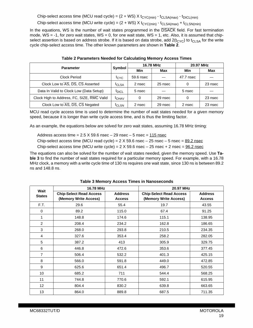
Table 2 Parameters Needed for Calculating Memory Access Times
Parameter Symbol16.78 MHz 20.97 MHz
Min Max Min Max
Clock Period tCYC 59.6 nsec --- 47.7 nsec ---
Clock Low to AS, DS, CS Asserted tCLSA 2 nsec 25 nsec 0 23 nsec
Data In Valid to Clock Low (Data Setup) tDICL 5 nsec --- 5 nsec ---
Clock High to Address, FC, SIZE, RMC Valid tCHAV 0 29 nsec 0 23 nsec
Clock Low to AS, DS, CS Negated tCLSN 2 nsec 29 nsec 2 nsec 23 nsec
Table 3 Memory Access Times in Nanoseconds
WaitStates
16.78 MHz 20.97 MHzChip-Select Read Access(Memory Write Access)
AddressAccess
Chip-Select Read Access(Memory Write Access)
AddressAccess
F.T. 29.6 55.4 19.7 43.55
0 89.2 115.0 67.4 91.25
1 148.8 174.6 115.1 138.95
2 208.4 234.2 162.8 186.65
3 268.0 293.8 210.5 234.35
4 327.6 353.4 258.2 282.05
5 387.2 413 305.9 329.75
6 446.8 472.6 353.6 377.45
7 506.4 532.2 401.3 425.15
8 566.0 591.8 449.0 472.85
9 625.6 651.4 496.7 520.55
10 685.2 711 544.4 568.25
11 744.8 770.6 592.1 615.95
12 804.4 830.2 639.8 663.65
13 864.0 889.8 687.5 711.35
MC68332TUT/D MOTOROLA19
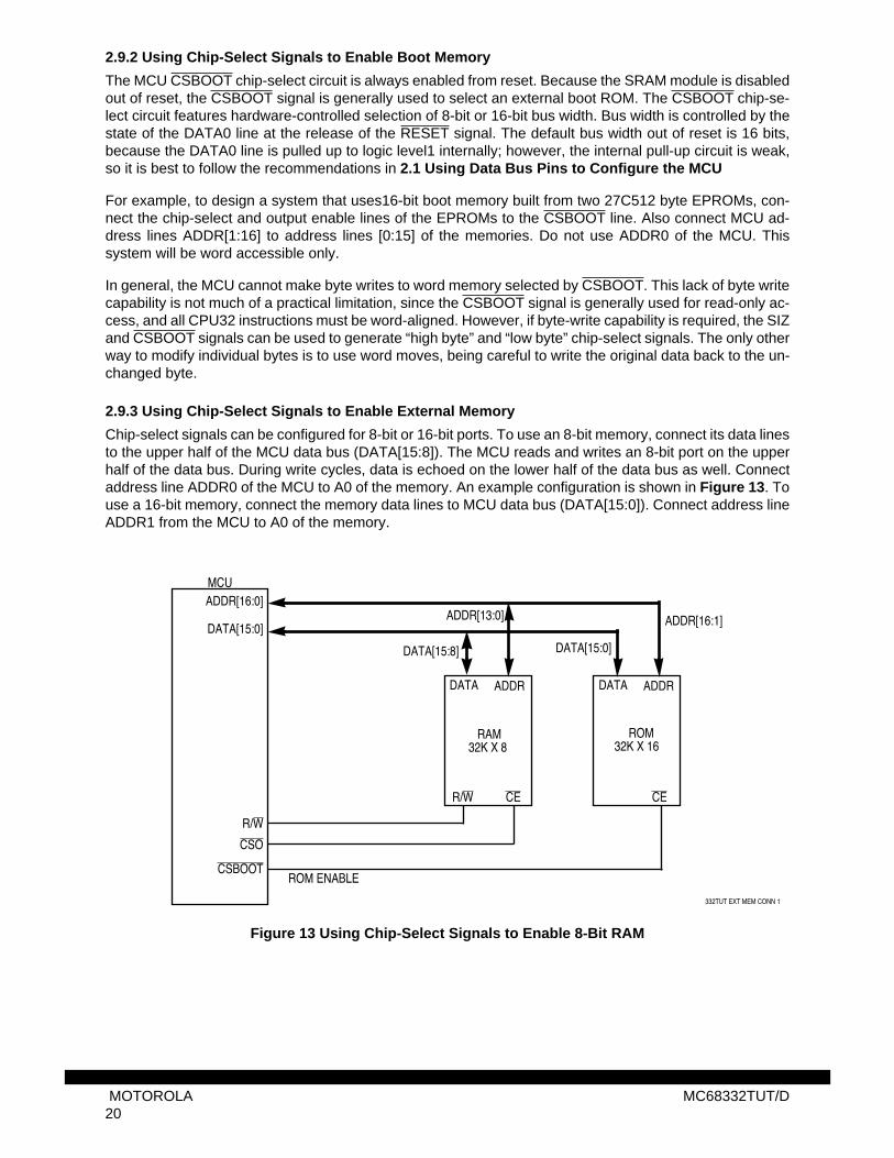
2.9.2 Using Chip-Select Signals to Enable Boot Memory
The MCU CSBOOT chip-select circuit is always enabled from reset. Because the SRAM module is disabledout of reset, the CSBOOT signal is generally used to select an external boot ROM. The CSBOOT chip-se-lect circuit features hardware-controlled selection of 8-bit or 16-bit bus width. Bus width is controlled by thestate of the DATA0 line at the release of the RESET signal. The default bus width out of reset is 16 bits,because the DATA0 line is pulled up to logic level1 internally; however, the internal pull-up circuit is weak,so it is best to follow the recommendations in 2.1 Using Data Bus Pins to Configure the MCU
For example, to design a system that uses16-bit boot memory built from two 27C512 byte EPROMs, con-nect the chip-select and output enable lines of the EPROMs to the CSBOOT line. Also connect MCU ad-dress lines ADDR[1:16] to address lines [0:15] of the memories. Do not use ADDR0 of the MCU. Thissystem will be word accessible only.
In general, the MCU cannot make byte writes to word memory selected by CSBOOT. This lack of byte writecapability is not much of a practical limitation, since the CSBOOT signal is generally used for read-only ac-cess, and all CPU32 instructions must be word-aligned. However, if byte-write capability is required, the SIZand CSBOOT signals can be used to generate “high byte” and “low byte” chip-select signals. The only otherway to modify individual bytes is to use word moves, being careful to write the original data back to the un-changed byte.
2.9.3 Using Chip-Select Signals to Enable External Memory
Chip-select signals can be configured for 8-bit or 16-bit ports. To use an 8-bit memory, connect its data linesto the upper half of the MCU data bus (DATA[15:8]). The MCU reads and writes an 8-bit port on the upperhalf of the data bus. During write cycles, data is echoed on the lower half of the data bus as well. Connectaddress line ADDR0 of the MCU to A0 of the memory. An example configuration is shown in Figure 13. Touse a 16-bit memory, connect the memory data lines to MCU data bus (DATA[15:0]). Connect address lineADDR1 from the MCU to A0 of the memory.
Figure 13 Using Chip-Select Signals to Enable 8-Bit RAM
332TUT EXT MEM CONN 1
MCUADDR[16:0]
DATA[15:0]
R/W
CSO
CSBOOTROM ENABLE
ADDR[16:1]
DATA
RAM32K X 8
ROM32K X 16
CE
ADDR[13:0]
R/W
DATA[15:8] DATA[15:0]
ADDR DATA ADDR
CE
MOTOROLA MC68332TUT/D20
2.9.3.1 How to Construct Word Memory from Two Byte Memories
For chip-select signals other than CSBOOT, forming word memory that is byte-accessible from two byte-wide devices is simple. Use a separate chip-select pin for each device, and configure chip-select logic todecode the upper and lower bytes, respectively. Each of the chip-select circuits must be configured as a 16-bit port, even though only eight bits of memory are being accessed.This allows both byte and word writes—if both memories were connected to the same chip-select line, byte writes would corrupt the adjacent byte.This function can also be implemented in external logic by gating a single chip-select line with the MCUADDR0 line to select upper and lower bytes. For ROM memory a single-chip-select can be used to enableboth byte-wide ROMs, as the MCU uses only the required byte on the data bus during a byte read and ig-nores the remaining byte.
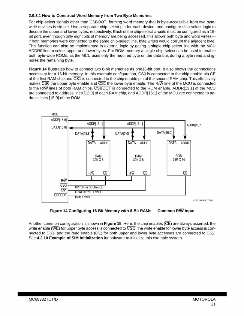
Figure 14 illustrates how to connect two 8-bit memories as one16-bit port. It also shows the connectionsnecessary for a 16-bit memory. In this example configuration, CS0 is connected to the chip enable pin CEof the first RAM chip and CS1 is connected to the chip enable pin of the second RAM chip. This effectivelymakes CS0 the upper byte enable and CS1 the lower byte enable. The R/W line of the MCU is connectedto the R/W lines of both RAM chips. CSBOOT is connected to the ROM enable. ADDR[13:1] of the MCUare connected to address lines [12:0] of each RAM chip, and ADDR[16:1] of the MCU are connected to ad-dress lines [15:0] of the ROM.
Figure 14 Configuring 16-Bit Memory with 8-Bit RAMs — Common R/W Input
Another common configuration is shown in Figure 15. Here, the chip enables (CE) are always asserted, thewrite enable (WE) for upper byte access is connected to CSO, the write enable for lower byte access is con-nected to CS1, and the read enable (OE) for both upper and lower byte accesses are connected to CS2.See 4.2.10 Example of SIM Initialization for software to initialize this example system.
332TUT EXT MEM CONN 2
MCU
ROM ENABLE
ADDR[16:1]
DATA
RAM32K X 8
ROM32K X 16
CE
ADDR[13:1]
R/W
DATA[7:0] DATA[15:0]
ADDR DATA ADDR
CE
DATA
RAM32K X 8
ADDR[13:1]
R/W
DATA[15:8]
ADDR
CE
LOWER BYTE ENABLE
UPPER BYTE ENABLE
ADDR[16:0]
DATA[15:0]
R/WCSO
CSBOOTCS1
MC68332TUT/D MOTOROLA21
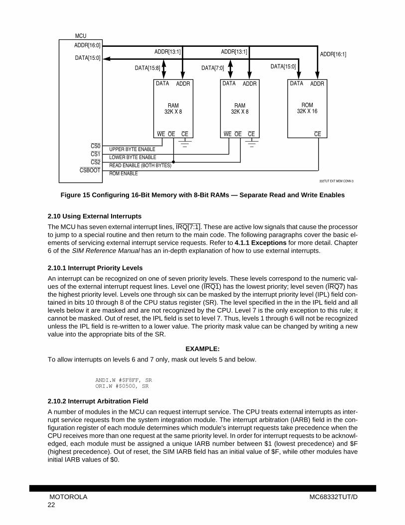
Figure 15 Configuring 16-Bit Memory with 8-Bit RAMs — Separate Read and Write Enables
2.10 Using External Interrupts
The MCU has seven external interrupt lines, IRQ[7:1]. These are active low signals that cause the processorto jump to a special routine and then return to the main code. The following paragraphs cover the basic el-ements of servicing external interrupt service requests. Refer to 4.1.1 Exceptions for more detail. Chapter6 of the SIM Reference Manual has an in-depth explanation of how to use external interrupts.
2.10.1 Interrupt Priority Levels
An interrupt can be recognized on one of seven priority levels. These levels correspond to the numeric val-ues of the external interrupt request lines. Level one (IRQ1) has the lowest priority; level seven (IRQ7) hasthe highest priority level. Levels one through six can be masked by the interrupt priority level (IPL) field con-tained in bits 10 through 8 of the CPU status register (SR). The level specified in the in the IPL field and alllevels below it are masked and are not recognized by the CPU. Level 7 is the only exception to this rule; itcannot be masked. Out of reset, the IPL field is set to level 7. Thus, levels 1 through 6 will not be recognizedunless the IPL field is re-written to a lower value. The priority mask value can be changed by writing a newvalue into the appropriate bits of the SR.
EXAMPLE:
To allow interrupts on levels 6 and 7 only, mask out levels 5 and below.
ANDI.W #$F8FF, SRORI.W #$0500, SR
2.10.2 Interrupt Arbitration Field
A number of modules in the MCU can request interrupt service. The CPU treats external interrupts as inter-rupt service requests from the system integration module. The interrupt arbitration (IARB) field in the con-figuration register of each module determines which module's interrupt requests take precedence when theCPU receives more than one request at the same priority level. In order for interrupt requests to be acknowl-edged, each module must be assigned a unique IARB number between $1 (lowest precedence) and $F(highest precedence). Out of reset, the SIM IARB field has an initial value of $F, while other modules haveinitial IARB values of $0.
332TUT EXT MEM CONN 3
MCU
ROM ENABLE
ADDR[16:1]
DATA
RAM32K X 8
ROM32K X 16
CE
ADDR[13:1]
DATA[7:0] DATA[15:0]
ADDR DATA ADDRDATA
RAM32K X 8
ADDR[13:1]
WE
DATA[15:8]
ADDR
CE
LOWER BYTE ENABLE
UPPER BYTE ENABLE
ADDR[16:0]
DATA[15:0]
CS0CS1
CSBOOTCS2
OE
READ ENABLE (BOTH BYTES)
WE CEOE
MOTOROLA MC68332TUT/D22
2.10.3 Interrupt Vectors
Vectors are 32-bit addresses that point to the interrupt service routines (and other exception handlers). Theyare stored in a data structure called the exception vector table. There are 256 vector addresses in the ex-ception vector table; of these, 199 can be used for interrupts. The base address of the exception vector tableis determined by the value stored in the vector base register. A vector number is used to calculate the vectoraddress, or displacement into the exception vector table.
2.10.4 The Interrupt Acknowledge Cycle
After the CPU recognizes a valid interrupt request, it begins the interrupt acknowledge (IACK) cycle. TheCPU changes the IPL mask value to the level of the acknowledged interrupt to preclude lower-or-equal pri-ority interrupt requests, then initiates a read cycle in CPU space. Since there is no dedicated IACK pin onthe MCU, an external IACK signal is usually provided by a chip-select pin. The CPU-space read serves twopurposes: it provides the address match required for chip-select assertion, and it acquires an interrupt vec-tor number.
Vector numbers can be supplied by the device requesting interrupt service, or they can be generated auto-matically. Vector numbers supplied by the device cause the CPU to access one of 192 user vectors in theexception vector table; automatically generated vectors cause the CPU to access one of the seven autovec-tors in the table. Each method of vector number acquisition requires a different form of IACK cycle termina-tion. If a vector number is supplied, either the requesting device must terminate the IACK cycle with aDSACK signal or the chip-select logic must generate the DSACK signal internally. If an autovector is used,an external device can assert the AVEC signal or an AVEC signal can be generated by the chip-select logic.Since normal bus cycles occur in user or supervisor space, but an IACK cycle occurs in CPU space, thesame chip-select circuit cannot be used to terminate both an IACK cycle and a normal bus cycle.
2.10.4.1 User Vectors
Once an interrupting device has placed a user vector number on the external data bus in response to anIACK signal from the MCU, either the device must terminate the IACK cycle with DSACK, or the chip-selectlogic must generate DSACK internally. When the bus cycle has been terminated, the vector number is left-shifted twice (multiplied by 4), then a 32-bit vector address is formed by concatenating the upper 22 bits ofthe vector base register, the shifted value, and %00. The CPU then saves the current context, loads the 32-bit vector into the PC, and begins to execute the service routine at that address.
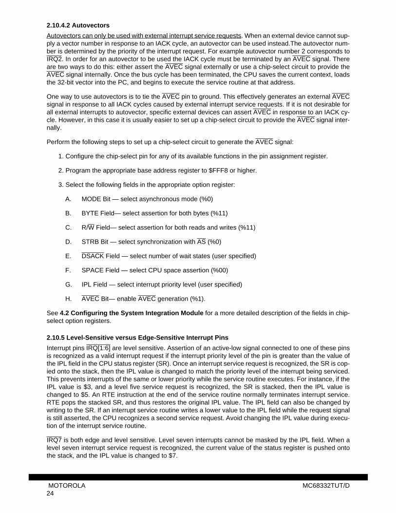
An example is shown in Figure 16. Chip select 1 is configured for interrupt acknowledge and automatic gen-eration of the DSACK signal. It is connected to the IACK pin of the peripheral. Because the processor drives$FFFFFx onto the address bus and drives the function code pins to indicate CPU space during an IACKcycle, the chip-select base address register must be programmed to $FFFX. When the CPU recognizes aninterrupt and initiates an IACK cycle, CS1 is asserted. In response, the peripheral drives an 8-bit vectornumber onto the data bus. Chip-select logic then terminates the IACK cycle with DSACK.
Figure 16 Chip-Select Line Used For Interrupt Acknowledge
332TUT PERI CONN
CS
D7
D0
IACK
D15
D8
CS0CS1
MC68332 PERIPHERAL
D6D14D5D13D4D12D3D11D2D10D1D9
MC68332TUT/D MOTOROLA23
2.10.4.2 Autovectors
Autovectors can only be used with external interrupt service requests. When an external device cannot sup-ply a vector number in response to an IACK cycle, an autovector can be used instead.The autovector num-ber is determined by the priority of the interrupt request. For example autovector number 2 corresponds toIRQ2. In order for an autovector to be used the IACK cycle must be terminated by an AVEC signal. Thereare two ways to do this: either assert the AVEC signal externally or use a chip-select circuit to provide theAVEC signal internally. Once the bus cycle has been terminated, the CPU saves the current context, loadsthe 32-bit vector into the PC, and begins to execute the service routine at that address.
One way to use autovectors is to tie the AVEC pin to ground. This effectively generates an external AVECsignal in response to all IACK cycles caused by external interrupt service requests. If it is not desirable forall external interrupts to autovector, specific external devices can assert AVEC in response to an IACK cy-cle. However, in this case it is usually easier to set up a chip-select circuit to provide the AVEC signal inter-nally.
Perform the following steps to set up a chip-select circuit to generate the AVEC signal:
1. Configure the chip-select pin for any of its available functions in the pin assignment register.
2. Program the appropriate base address register to $FFF8 or higher.
3. Select the following fields in the appropriate option register:
A. MODE Bit — select asynchronous mode (%0)
B. BYTE Field— select assertion for both bytes (%11)
C. R/W Field— select assertion for both reads and writes (%11)
D. STRB Bit — select synchronization with AS (%0)
E. DSACK Field — select number of wait states (user specified)
F. SPACE Field — select CPU space assertion (%00)
G. IPL Field — select interrupt priority level (user specified)
H. AVEC Bit— enable AVEC generation (%1).
See 4.2 Configuring the System Integration Module for a more detailed description of the fields in chip-select option registers.
2.10.5 Level-Sensitive versus Edge-Sensitive Interrupt Pins
Interrupt pins IRQ[1:6] are level sensitive. Assertion of an active-low signal connected to one of these pinsis recognized as a valid interrupt request if the interrupt priority level of the pin is greater than the value ofthe IPL field in the CPU status register (SR). Once an interrupt service request is recognized, the SR is cop-ied onto the stack, then the IPL value is changed to match the priority level of the interrupt being serviced.This prevents interrupts of the same or lower priority while the service routine executes. For instance, if theIPL value is $3, and a level five service request is recognized, the SR is stacked, then the IPL value ischanged to $5. An RTE instruction at the end of the service routine normally terminates interrupt service.RTE pops the stacked SR, and thus restores the original IPL value. The IPL field can also be changed bywriting to the SR. If an interrupt service routine writes a lower value to the IPL field while the request signalis still asserted, the CPU recognizes a second service request. Avoid changing the IPL value during execu-tion of the interrupt service routine.
IRQ7 is both edge and level sensitive. Level seven interrupts cannot be masked by the IPL field. When alevel seven interrupt service request is recognized, the current value of the status register is pushed ontothe stack, and the IPL value is changed to $7.
MOTOROLA MC68332TUT/D24
It is very important to make certain that the IRQ7 signal be de-asserted before the level seven interrupt ser-vice routine ends. A new level seven interrupt will be recognized in the following cases:
If the IRQ7 signal de-asserts and is then re-asserted while the interrupt service routine is executing.
If the IRQ7 signal remains asserted until the RTE instruction that ends the service routine is executed.
If the IRQ7 signal is asserted and the IPL field is written during execution of the interrupt service routine.This is true even when the mask is re-written to $7.
Provide for de-assertion of the signal within the service routine, and avoid writing to the SR during executionof the level seven interrupt service routine.
2.10.6 Checklist for External Interrupt Acknowledge
• Is the desired pin configured as an interrupt pin instead of an I/O pin?
The interrupt pins are dual-function pins. Their initial configuration is determined by the state of databus pin 9 at the release of reset. After reset, their configuration is determined by the port F pin assign-ment register.
• Was the starting address of the interrupt routine written to the vector offset address?
The CPU must be told where the interrupt service routine begins. See 4.1.1 Exceptions for a more de-tailed explanation.
• Is the IARB field in the SIMCR a unique, non-zero value between $1 and $F?
All interrupting modules must have a unique, non-zero value in the IARB field
• Is the IPL field in the CPU status register set to a value lower than the desired interrupt level?
The CPU will not recognize an interrupt that is at the same level or lower than the value in the IPL field.Level 7 is the only exception to this rule; it is always recognized.
• Is the IACK cycle terminated with AVEC or DSACK?
The IACK cycle must be terminated by assertion of the AVEC or DSACK signals, or a chip-select circuitmust be configured to assert AVEC or DSACK internally.
• Does the interrupt request signal de-assert inside the exception handler?
It is a good idea to control de-assertion of the interrupt in software. The interrupt should be de-assertedbefore the RTE instruction.
MC68332TUT/D MOTOROLA25
3 ESTABLISHING COMMUNICATION
3.1 Communicating with the Target Board
After a target board has been built, it is generally necessary to communicate with it for debugging purposes.Although a designer can write a ROM monitor or modify CPU32Bug to communicate with the MCU via theserial port, it is simpler and often more effective to use an emulator or the CPU32 background debug mode(BDM) for communication.
3.1.1 Using an Emulator
An emulator is a direct replacement for the chip that is used to evaluate both software and signals on thetarget board. Emulators can be very sophisticated and costly, but are very useful in tracking down designproblems because they allow the designer to see exactly what the MCU is doing at every step of operation.When both the board and code are fully debugged, the emulator is removed and the MCU is placed on theboard.
3.1.2 Using Background Debug Mode
Background debug mode is a special CPU operating mode that allows an external host to take control ofthe MCU. BDM is a very useful tool for debugging. During BDM operation, normal instruction execution issuspended, and microcode executes built-in debugging instructions under external control. Since BDM sus-pends processor execution, an external host can examine and change memory and registers. BDM instruc-tions and the protocol required to use them are described in detail in the CPU32 Reference Manual.AN1230/D, A BDM Driver Package for Modular Microcontrollers shows how to implement a BDM commu-nication interface using C language drivers.
While a BDM interface is relatively easy to implement, ready-made BDM interfaces are inexpensive and re-liable. Motorola sells the M68ICD32 BDM debugger made by P&E Microcomputer Systems. The M68ICD32consists of the necessary cable and software to implement BDM debugging on an IBM-compatible PC. Allthe discussions in this section assume that M68ICD32 is being used.
3.1.2.1 BDM Signals
To use BDM, simply connect ten MCU lines to pins on the development board that are spaced so that afemale Berg connector can plug into them. Figure 17 shows the pinouts for the recommended 10-pin BDMconnector. Table 4 describes the BDM signals. Refer to 3.2.1.2 Using the EVK in Background DebugMode for a discussion of the older, 8-pin connector.
Figure 17 10-Pin BDM Connector
332TUT BERG10
GND
RESET
VDD
2
4
6
8
10
DS
GND
1
3
5
7
9
BERR
BKPT/DSCLK
FREEZE
IPIPE1/DSI
IPIPE0/DS0
MOTOROLA MC68332TUT/D26
Only ten pins on the board, a special cable, and software are needed to debug. The M68ICD32 cable hasa 10-pin female connector on one end and a PAL with a 25-pin connector on the other end. The 10-pin con-nector will plug directly into a male header or connector with the layout shown in Figure 17. The PAL endof the cable plugs into the parallel port of a PC. The PC runs the debugger software that controls the MCUin BDM.
3.1.2.2 How BDM Works
The debugger causes the MCU to enter debugging mode by driving the BKPT pin low at the release of theRESET signal. Reset causes the MCU to fetch the reset exception vectors, load the program counter andstack pointer, then fetch the first instruction pointed to. Since the SRAM module is disabled out of reset,reset vector fetches are made from external memory enabled by the CSBOOT signal. If the CSBOOT chip-select circuit is configured to enable a 16-bit port (DATA0 = 1 at release of RESET), the first word of theinstruction is fetched, however, if the CSBOOT chip-select circuit is configured to enable an 8-bit port(DATA0 held low at the release of RESET), the MCU fetches the first byte of the instruction. The MCU thenenters BDM.
At this point the debugger causes the MCU to fetch several instructions, which are displayed in the debug-ger window on the computer screen. If valid stack pointer and program counter values are present, and avalid program is resident at the address pointed to by the initial PC value, the debugger will display the codebeginning at the program counter address.
If the initial stack pointer and program counter values are not valid, however, or if the external memory iseither not connected or uninitialized when the fetches are made, it is very likely that the initial SP and PCvalues will be $FFFFFFF. CSBOOT is the only chip-select circuit that is active out of reset, and it enablesonly the first 1 Mbyte of memory — when the first instruction fetches are made at $FFFFFF, there will benothing to generate DSACK and terminate the bus cycle, and the debugger software will force a bus error.Should this occur, the debugger generally displays a series of “Memory implementation error: debuggersupplied DSACK” messages on the computer screen. After the debugger software has finished making thescheduled number of program fetches, the error messages will stop, and the MCU will be in BDM waitingfor the next debugger command. However, additional errors will occur if the next command is an externalmemory access because the program counter and stack pointer values are invalid.
When using a software background mode debugger to boot an MCU from external RAM or uninitializedROM, it is imperative that the following actions be taken immediately after starting the debugger:
1. Load a value into address register A7 to serve as a stack pointer value. It must point to a modifiablememory address.
2. Load the address of the first instruction to be executed into the program counter.
Table 4 BDM Connections
10-Pin Connector 8-Pin Connector Signal Use
1 ---- DS Data Strobe
2 ---- BERR Output from ICD to BERR input
3 1 GND Ground Reference
4 2 BKPT/DSCLKOutput from ICD to BKPT input; assertion causes MCU to first enable and then enter background mode. Once in BDM, this pin becomes the serial clock.
5 3 GND Ground Reference
6 4 FREEZEOutput from MCU indicating whether it is operating normal-ly or is in BDM
7 5 RESET Device reset
8 6 IFETCH/DSI Serial input data to the MCU in BDM
9 7 VDD Device Operating Voltage
10 8 IPIPE/DSO Serial output data from the MCU in BDM
MC68332TUT/D MOTOROLA27
The debugger should now work reliably. That is, programs can be downloaded into the RAM and executed.Alternatively, write the reset vector to memory location $000000. The reset vector is discussed in detail in4.1.3.1 Initializing the Reset Vector
3.2 Communicating with Motorola Boards
Third party vendors sell many types of development tools to help establish communication with the MCU.These tools are described in the Motorola Microcontroller Development Tools Directory. However, this tu-torial focuses only on Motorola evaluation boards.
3.2.1 The M68EVK332
The M68EVK332 (A or G) is an evaluation kit that consists of two components: a platform board (PFB) anda business card computer (BCC). The PFB has logic analyzer connectors and sockets for external memory.The BCC is a plug-in daughter board that holds the MCU, RAM, and a boot EPROM. On older versions ofthe BCC, the EPROM is soldered to the board and cannot be easily reprogrammed. However, on newerversions of the BCC, the EPROM is socketed and can easily be removed and reprogrammed.
There are two ways to communicate with the EVK: serial communication using the ROM monitor in theEPROM and background debug mode (BDM) using a debugger. Both are valid ways of debugging code;however, the user interface for BDM is much more user-friendly.
3.2.1.1 Communication Using the ROM Monitor
The EPROM contains a monitor program called CPU32Bug (332Bug in older versions of the BCC).CPU32Bug consists of both initialization code and a user interface. The initialization code sets the systemclock to 16.778 MHz, disables the software watchdog, and configures chip-selects 0, 1, and 2, which arenecessary to talk to the RAM. The user interface uses the serial communication interface (SCI) to give aprompt on a computer screen and allow the user to modify memory, load, trace, and run programs. TheCPU32Bug Debug Monitor User’s Manual explains more about the capabilities of CPU32Bug.
Terminal emulation programs for the Macintosh, such as MacTerminal or Red Ryder, and communicationssoftware for the IBM-PC, such as Kermit or PROCOMM, are acceptable for use with the EVK. TheM68332EVK Evaluation Kit User’s Manual explains the necessary steps to follow for each type of software.This section will only explain how to use PROCOMM with the EVK.
First, assemble a cable as shown in Figure 18. The 25-pin connector goes to the serial port on the PC, andthe 9-pin connector goes to P9 (terminal from BCC) on the EVK. Connect the cable from the appropriate 9-pin serial port on the EVK to the serial port on the PC. Then, execute the communications program. As anexample, for PROCOMM PLUS, set up PROCOMM to match the EVK baud rate and protocol as follows:
9600 baud, no parity, 8 bits, 1 stop bit, full duplex
Set up ASCII transfer parameters as follows:
Echo Local - NoExpand Blank Lines - YesPace Character - 0Character pacing - 15 (milliseconds)Line pacing - 10CR Translation - NoneLF Translation - None
Now, apply power to the EVK and press the keyboard carriage return (<CR>) key to display the EVK monitorprompt. If necessary, press the BCC RESET button on the EVK.
To load a program, perform the following sequence:
CPU32Bug>LO (Press <CR>)
MOTOROLA MC68332TUT/D28
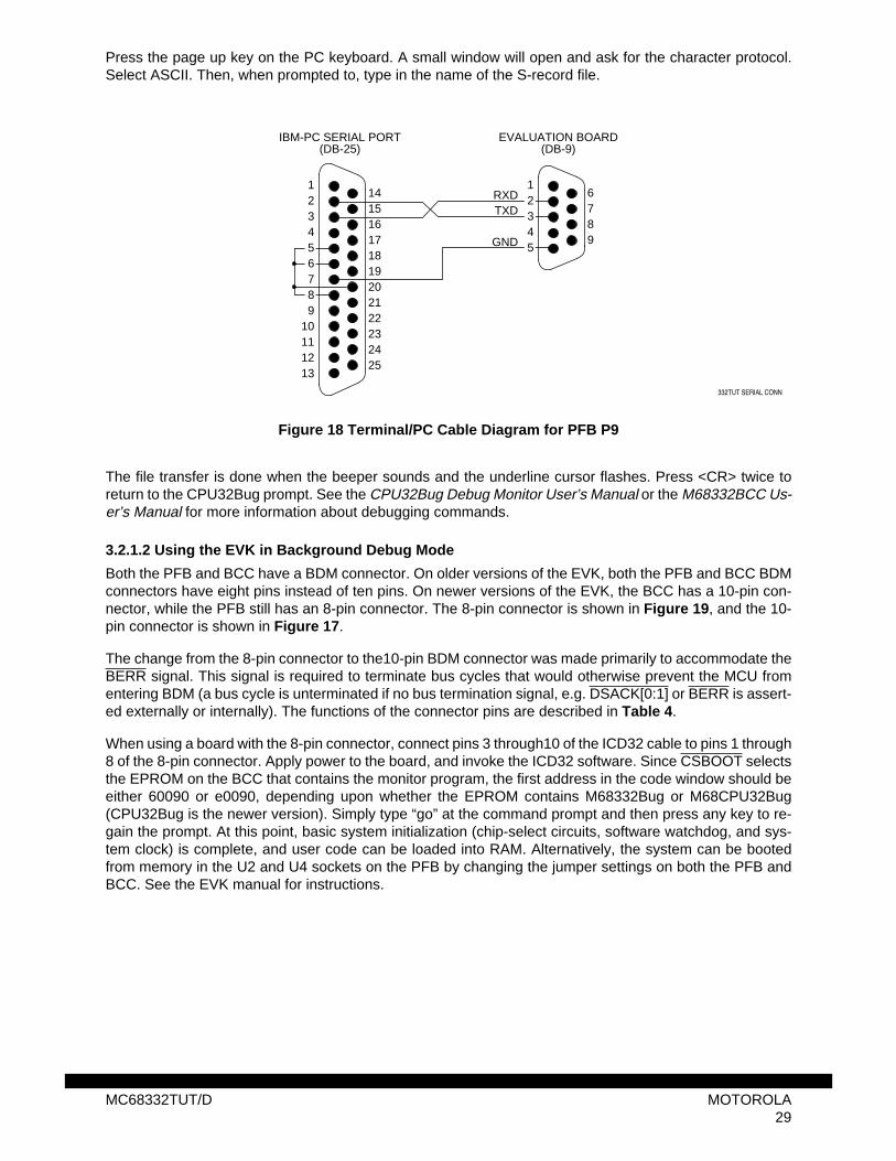
Press the page up key on the PC keyboard. A small window will open and ask for the character protocol.Select ASCII. Then, when prompted to, type in the name of the S-record file.
Figure 18 Terminal/PC Cable Diagram for PFB P9
The file transfer is done when the beeper sounds and the underline cursor flashes. Press <CR> twice toreturn to the CPU32Bug prompt. See the CPU32Bug Debug Monitor User’s Manual or the M68332BCC Us-er’s Manual for more information about debugging commands.
3.2.1.2 Using the EVK in Background Debug Mode
Both the PFB and BCC have a BDM connector. On older versions of the EVK, both the PFB and BCC BDMconnectors have eight pins instead of ten pins. On newer versions of the EVK, the BCC has a 10-pin con-nector, while the PFB still has an 8-pin connector. The 8-pin connector is shown in Figure 19, and the 10-pin connector is shown in Figure 17.
The change from the 8-pin connector to the10-pin BDM connector was made primarily to accommodate theBERR signal. This signal is required to terminate bus cycles that would otherwise prevent the MCU fromentering BDM (a bus cycle is unterminated if no bus termination signal, e.g. DSACK[0:1] or BERR is assert-ed externally or internally). The functions of the connector pins are described in Table 4.
When using a board with the 8-pin connector, connect pins 3 through10 of the ICD32 cable to pins 1 through8 of the 8-pin connector. Apply power to the board, and invoke the ICD32 software. Since CSBOOT selectsthe EPROM on the BCC that contains the monitor program, the first address in the code window should beeither 60090 or e0090, depending upon whether the EPROM contains M68332Bug or M68CPU32Bug(CPU32Bug is the newer version). Simply type “go” at the command prompt and then press any key to re-gain the prompt. At this point, basic system initialization (chip-select circuits, software watchdog, and sys-tem clock) is complete, and user code can be loaded into RAM. Alternatively, the system can be bootedfrom memory in the U2 and U4 sockets on the PFB by changing the jumper settings on both the PFB andBCC. See the EVK manual for instructions.
332TUT SERIAL CONN
141516171819202122232425
6789
123456789
10111213
12345
RXDTXD
GND
IBM-PC SERIAL PORT(DB-25)
EVALUATION BOARD(DB-9)
MC68332TUT/D MOTOROLA29
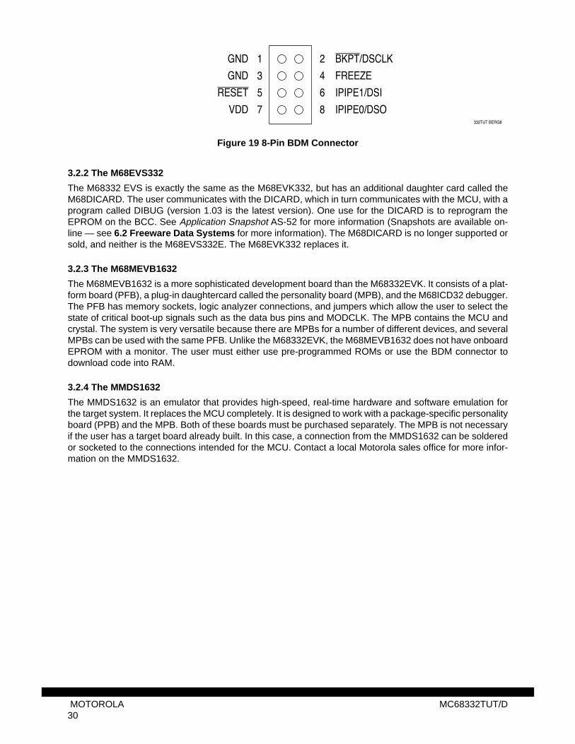
Figure 19 8-Pin BDM Connector
3.2.2 The M68EVS332
The M68332 EVS is exactly the same as the M68EVK332, but has an additional daughter card called theM68DICARD. The user communicates with the DICARD, which in turn communicates with the MCU, with aprogram called DIBUG (version 1.03 is the latest version). One use for the DICARD is to reprogram theEPROM on the BCC. See Application Snapshot AS-52 for more information (Snapshots are available on-line — see 6.2 Freeware Data Systems for more information). The M68DICARD is no longer supported orsold, and neither is the M68EVS332E. The M68EVK332 replaces it.
3.2.3 The M68MEVB1632
The M68MEVB1632 is a more sophisticated development board than the M68332EVK. It consists of a plat-form board (PFB), a plug-in daughtercard called the personality board (MPB), and the M68ICD32 debugger.The PFB has memory sockets, logic analyzer connections, and jumpers which allow the user to select thestate of critical boot-up signals such as the data bus pins and MODCLK. The MPB contains the MCU andcrystal. The system is very versatile because there are MPBs for a number of different devices, and severalMPBs can be used with the same PFB. Unlike the M68332EVK, the M68MEVB1632 does not have onboardEPROM with a monitor. The user must either use pre-programmed ROMs or use the BDM connector todownload code into RAM.
3.2.4 The MMDS1632
The MMDS1632 is an emulator that provides high-speed, real-time hardware and software emulation forthe target system. It replaces the MCU completely. It is designed to work with a package-specific personalityboard (PPB) and the MPB. Both of these boards must be purchased separately. The MPB is not necessaryif the user has a target board already built. In this case, a connection from the MMDS1632 can be solderedor socketed to the connections intended for the MCU. Contact a local Motorola sales office for more infor-mation on the MMDS1632.
332TUT BERG8
RESET
VDD
2
4
6
8
GND
GND
1
3
5
7
BKPT/DSCLK
FREEZE
IPIPE1/DSI
IPIPE0/DSO
MOTOROLA MC68332TUT/D30
4 SYSTEM INITIALIZATION
4.1 Configuring the Central Processing Unit
Initial stack pointer and program counter values are fetched from boot ROM. Other CPU resources that mustbe initialized include the vector base register, the exception vector table, and the CPU status register.
4.1.1 Exceptions
An exception is a special condition, such as a reset, an interrupt, or an address error, that pre-empts normalprocessing. When the processor recognizes an exception, it jumps to a special address and executes codestarting at that address until it reaches a return from exception (RTE) instruction. Then, it resumes executionof the normal program code. The vectors in the exception vector table tell the processor the starting addressof each exception routine. The vector base register (VBR) determines the location of the vector table inmemory.
4.1.2 Vector Base Register
The vector base register is initialized to $000000 at reset, but the table can later be moved by changing thevalue in the VBR. Changing the address of the table does not alter the vectors it contains. Use a MOVECinstruction to access the VBR.
4.1.3 Exception Vector Table
The CPU32 recognizes 256 exception vector numbers. Each vector number corresponds to a space in theexception vector table that is two words long. Thus, the table extends 1024 bytes upward in memory fromthe base address. Each of the spaces in the table contains a 32-bit value that is used as an address pointer,or vector. The actual address of each of the vectors in the table, referred to as the vector address, is fourtimes the vector number plus the vector base address.
Table 5 is an overview of the exception vector table. Refer to SECTION 6 EXCEPTION PROCESSING intheCPU32 Reference Manual for detailed discussion of exception processing and a complete list of excep-tion vectors.
The first two spaces (four words) in the exception vector table are used for initial stack pointer and programcounter values. These are referred to collectively as the reset vector, because the CPU32 loads the SP andPC sequentially during reset exception processing. Unlike other vectors, the reset vector is mapped to su-pervisor program space, to facilitate fetching the values. Because the VBR is initialized to $000000 duringreset, the reset vector is always located at address $000000.
All the other exception vectors occupy two words in the table, and are located in supervisor data space.These vectors point to the beginning of software routines that handle particular exceptions. All the vectorsin the exception vector table must be initialized. While the reset vector is generally fetched from externalROM, correct initial values for the stack pointer and program counter must be written to addresses $000000to $000006 in order for the system to begin program execution.
Here’s how the exception vector table works. Assume that the vector table base address is the default value,$000000. An external device asserts IRQ7, and the CPU acknowledges the interrupt service request. Theexternal device must either provide a user vector number on the data bus and then terminate the bus cycleby asserting DSACK, or it must assert AVEC and let the processor supply the level 7 autovector number,which is 31. Assuming the external device asserts AVEC, vector number 31 is supplied to the CPU32. TheCPU32 multiplies the vector number by four to calculate the vector offset, then adds the vector offset to thecontents of the VBR. The sum is the memory address that contains the starting address of the exceptionroutine. In this case, since VBR content is $000000, the vector offset is 31 X 4 = 124 = $7C. The CPU readsaddress $7C and uses the 32-bit number it contains as the starting address of the interrupt service routine.
MC68332TUT/D MOTOROLA31
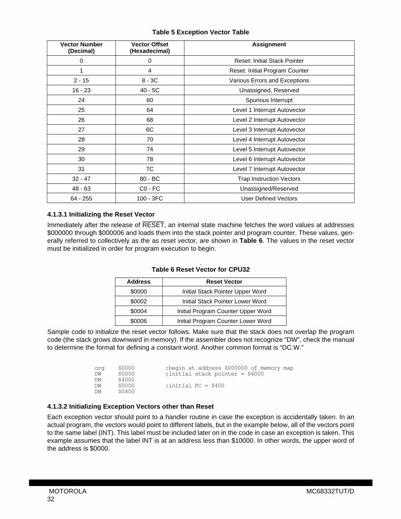
4.1.3.1 Initializing the Reset Vector
Immediately after the release of RESET, an internal state machine fetches the word values at addresses$000000 through $000006 and loads them into the stack pointer and program counter. These values, gen-erally referred to collectively as the as reset vector, are shown in Table 6. The values in the reset vectormust be initialized in order for program execution to begin.
.
Sample code to initialize the reset vector follows. Make sure that the stack does not overlap the programcode (the stack grows downward in memory). If the assembler does not recognize “DW”, check the manualto determine the format for defining a constant word. Another common format is “DC.W.”
org $0000 ;begin at address $000000 of memory mapDW $0000 ;initial stack pointer = $4000DW $4000DW $0000 ;initial PC = $400DW $0400
4.1.3.2 Initializing Exception Vectors other than Reset
Each exception vector should point to a handler routine in case the exception is accidentally taken. In anactual program, the vectors would point to different labels, but in the example below, all of the vectors pointto the same label (INT). This label must be included later on in the code in case an exception is taken. Thisexample assumes that the label INT is at an address less than $10000. In other words, the upper word ofthe address is $0000.
Table 5 Exception Vector Table
Vector Number (Decimal)
Vector Offset (Hexadecimal)
Assignment
0 0 Reset: Initial Stack Pointer
1 4 Reset: Initial Program Counter
2 - 15 8 - 3C Various Errors and Exceptions
16 - 23 40 - 5C Unassigned, Reserved
24 60 Spurious Interrupt
25 64 Level 1 Interrupt Autovector
26 68 Level 2 Interrupt Autovector
27 6C Level 3 Interrupt Autovector
28 70 Level 4 Interrupt Autovector
29 74 Level 5 Interrupt Autovector
30 78 Level 6 Interrupt Autovector
31 7C Level 7 Interrupt Autovector
32 - 47 80 - BC Trap Instruction Vectors
48 - 63 C0 - FC Unassigned/Reserved
64 - 255 100 - 3FC User Defined Vectors
Table 6 Reset Vector for CPU32
Address Reset Vector
$0000 Initial Stack Pointer Upper Word
$0002 Initial Stack Pointer Lower Word
$0004 Initial Program Counter Upper Word
$0006 Initial Program Counter Lower Word
MOTOROLA MC68332TUT/D32
org $0008 ;put the following code in memory after the reset vector.DW $0000 ;The address of label INT is stored at location $0008,DW INT ;which is the bus error vectorDW $0000 ;address error -- location $000CDW INTDW $0000 ;illegal instruction -- location $0010DW INTDW $0000 ;zero division -- location $0014DW INTDW $0000 CHK, CHK2 Instructions -- location $0018DW INTDW $0000 ;Last User Defined Interrupt -- stored at location $03FCDW INT
In the actual program code, the following routine must be included:
INT code to handlethe exceptiongoes hereRTE ;return to the code that was previously being executed
4.1.4 CPU Status Register
The CPU status register contains some very important information.The SR is discussed on page 2-3 of theCPU32 Reference Manual. The fields are briefly described below:
Trace Enable [15:14] — If enabled, these bits cause the CPU to generate a trace exception after eachinstruction executes, allowing a debugging program to monitor the execution of a program under test.Out of reset, tracing is disabled. See page 6-13 in the CPU32 Reference Manual for more details.
Supervisor/User State [13] — The MCU has two privilege levels: supervisor and user. Not all registersand instructions are available at the user level. Most programs operate at the user level and then passcontrol to a supervisor routine by causing an exception. Out of reset, the supervisor/user state bit is set,which means that the MCU is in supervisor mode. See pages 5-2 to 5-3 in the CPU32 Reference Man-ual for more details.
Interrupt Priority Level[10:8] — The interrupt priority level determines which interrupts are recognizedand which are masked. Level 7 interrupts are always recognized. To allow other interrupts, this fieldmust contain a value that is lower than the interrupt priority level desired. For example, to allow level 6interrupts, the value must be %101 or less. Out of reset, the field has a value of %111, which disablesall interrupts except for level 7 interrupts.
Condition Code Register [4:0] — The bits in the condition code register reflect the results of a previousoperation, and can be used for various condition tests, including conditional branches. There are ex-tend, negative, zero, overflow, and carry bits.
4.2 Configuring the System Integration Module
Since the SIM determines important operating characteristics of the entire MCU, it should be the first moduleafter the CPU to be initialized. The following paragraphs discuss registers that it is important to initialize cor-rectly.
4.2.1 System Integration Module Configuration Register (SIMCR)
The SIMCR controls module mapping for the MCU, internal use of the FREEZE signal, and the precedenceof simultaneous interrupt requests of the same priority. Configure the SIMCR as follows.
1. Set the state of the module mapping (MM) bit. Its reset state is a one, and it is one-time writable. MMdetermines where the internal control registers are located in the system memory map. When MM =0, register addresses range from $7FF000 to $7FFFFF; when MM =1, register addresses range from$FFF000 to $FFFFFF.
MC68332TUT/D MOTOROLA33
2. If using the software watchdog, periodic interrupt timer, or the bus monitor, select action taken whenFREEZE is asserted. The freeze software enable (FRZSW) bit determines whether the softwarewatchdog and periodic interrupt timer counters continue to run when FREEZE is asserted, and thefreeze bus monitor enable (FRZBM) bit determines whether the bus monitor continues to operatewhen FREEZE is asserted.
3. Select the interrupt arbitration level for the SIM with the interrupt arbitration (IARB) field. The defaultstate out of reset is $F, the highest precedence. To avoid spurious interrupts, each module request-ing interrupts must have a unique, non-zero value in the IARB field. The CPU treats external interruptrequests as SIM interrupts.
4.2.2 Clock Synthesizer Control Register (SYNCR)
SYNCR controls clock frequency, clock reference failure, clock signal usage during low-power stop, and fre-quency of the 6800 bus clock output (ECLK). Configure SYNCR as follows.
1. Set frequency control bits (W,X,Y) to specify frequency.
2. Select action to be taken during loss of crystal (RSTEN bit): activate a system reset or operate in limpmode.
3. Select system clock during LPSTOP (STSIM and STEXT bits).
4. If using the ECLK, select the ECLK frequency (EDIV bit).
4.2.3 System Protection Control Register (SYPCR)
SYPCR controls the software watchdog, which is enabled out of reset. This means that, unless the SWE bitis cleared, a program must write the appropriate service sequence to the software service register (SWSR)in a defined period or the MCU will reset each time the watchdog times out.
1. Disable the software watchdog, if desired, by clearing the SWE bit.
2. If the watchdog is enabled, perform the following actions.
A. Choose whether to prescale the software watchdog clock (SWP bit).
B. Select the time-out period (SWT bits).
3. Enable the double bus fault monitor, if desired (DATAFE bit or HME bit).
4. Enable the external bus monitor (BME bit) if desired.
5. Select the time-out period for bus monitor (BMT bits).
4.2.4 Periodic Interrupt Timer Register (PITR)
PITR and PICR control the periodic interrupt timer (PIT). The PIT begins to run when a timing modulus iswritten to the PITM field in PITR. However, interrupt requests from the PIT are recognized only after an in-terrupt priority level is written into the PIRQL field in the PICR. Clearing PITM stops the timer; clearingPIRQL disables interrupts, but the timer continues to run. Because the CPU treats external interrupts asSIM interrupt requests, PIT interrupts take precedence over external interrupts of the same priority. To usethe timer, proceed as follows.
1. Make certain that there is a vector to the interrupt service routine in the exception vector table, andthat there is a service routine at the address pointed to.
2. Select whether or not to prescale the timer clock signal (PTP bit in PITR).
3. Select the timing modulus or interrupt rate (PITM field in PITR).
MOTOROLA MC68332TUT/D34
4.2.5 Periodic Interrupt Control Register (PICR)
1. Determine the appropriate PIT vector number and interrupt priority.
2. Write vector number and interrupt priority to PIV and PIRQL fields in PICR.
4.2.6 Chip-Select Pin Assignment Registers (CSPAR0 and CSPAR1)
The chip-select pins can be used in a number of ways. CSPAR determine the functions of the pins.
1. Set up the chip-select pins for discrete output, 8-bit chip-select operation, 16-bit chip-select operation,or alternate function.
2. If a chip-select circuit is used to generate an interrupt acknowledge signal, it must be configured forchip-select operation. However, if a chip-select circuit is used to generate an autovector, the pin canalso be used for discrete output or its alternate function.
4.2.7 Chip-Select Base Address Registers (CSBARBT, CSBAR[0:10])
Chip-select signals are asserted when the CPU accesses certain ranges of addresses. The base addressregisters specify the address ranges for each chip-select circuit.
1. Reprogram the base address and/or blocksize of CSBOOT if desired. The default value out of resetis a base address of $000000 with a blocksize of 1 MByte.
2. Program the base address and block size for each chip-select circuit that used. The base addressmust be on a word boundary of the block size. For example, for an 8 Kbyte block size, the base ad-dress can be $2000, $4000, $6000, $8000, etc. If a chip-select circuit is used to generate an interruptacknowledge signal or an autovector, the base address register must be set to $FFF8 or higher be-cause interrupt acknowledge cycles occur in CPU space.
4.2.8 Chip-Select Option Registers (CSORBT and CSOR[0:10])
The option registers control the conditions under which a chip-select signal is asserted.
1. Reprogram the options for CSBOOT if desired. Reducing the number of wait states from the resetvalue of 13 increases execution speed.
2. Program the option registers for each chip-select circuit used.
A. MODE — Select asynchronous mode (%0) unless using the ECLK output to provides synchronousbus timing for 6800 peripherals. In synchronous mode (%1), the STRB and DSACK fields haveno effect.
B. BYTE — This field determines whether to assert the chip-select signal for an upper-byte access,lower-byte access, both, or neither. When two 8-bit memories are used to make up one16-bit port,the associated chip-select circuits are programmed identically except for BYTE field values—se-lect upper byte for one and lower byte for the other.
C. R/W — This field specifies whether to assert the chip-select signal during a read cycle, a write cy-cle, or both.When the chip-select circuit is used to generate an IACK signal or to provide an au-tovector, this field must be set to “read.”
D. STRB — This field specifies whether chip-select assertion is synchronous with AS or DS. If a chip-select circuit is used to generate an IACK signal or to provide an autovector, this field should beset to “AS.”
E. DSACK — This field either specifies the number of wait states to insert before the chip-select cir-cuit asserts DSACK and terminates the bus cycle, or it specifies that the external device must pro-vide the DSACK signal by driving the external DSACK pins. Assertion of the external DSACK pinswill terminate a bus cycle even if the DSACK field is programmed for a certain number of wait
MC68332TUT/D MOTOROLA35
states. If a chip-select circuit is used to provide an autovector, fast termination is automaticallyselected, and the DSACK field is not used. For more information on how to determine the numberof wait states needed, see 2.9.1 Using Chip-Selects to Generate DSACK
F. SPACE — This field indicates the address space of the access. To access memory, select super-visor/user space. For IACK cycles, select CPU space.
G. IPL — If the chip-select circuit is used to provide an IACK signal or AVEC, the IPL field indicatesthe interrupt priority level selected.
H. AVEC — This field determines whether a chip-select circuit generates an autovector in responseto an IACK initiated by the assertion of an IRQ pin. For normal bus cycles, this field is not used. Ifa chip-select circuit is to be used to generate an IACK signal, program this field to zero to disableautovector generation. If a chip-select is to be used to generate an autovector, program this fieldto one.
4.2.9 General-Purpose I/O Ports
Certain SIM pins can be configured as general-purpose I/O ports when not used for other purposes. Port Epins share function with bus-control signals, port F pins share function with interrupt request signals, andport C (output only) pins share functions with chip-select signals. The ports are controlled by pin assignmentregisters (CSPAR, PEPAR, and PFPAR) and data direction registers (DDRE and DDRF). Pin assignmentregisters determine whether a pin is used for general-purpose I/O or for another function. Data direction reg-isters determine whether an I/O pin is an input or an output. Data is written to and read from the port dataregisters (PORTC, PORTE and PORTF).
1. Assign port pins by writing to pin assignment registers.
2. Program the data direction registers to assign input or output function to port pins
3. Use the port data registers to read/write data.
4.2.10 Example of SIM Initialization
This example assumes that two other files, org00000.asm and org00008.asm, exist. The file org00000.asminitializes the stack pointer and program counter. It contains the code shown in 4.1.3.1 Initializing the Re-set Vector. The file org00008.asm initializes the interrupt vectors. It contains the code shown in 4.1.3.2 Ini-tializing Exception Vectors other than Reset. This file is not necessary for debugging, but should beincluded in final application code. The code can be assembled with the IASM32 assembler.
CSBARBT EQU $FFFA48CSBAR0 EQU $FFFA4CCSBAR1 EQU $FFFA50CSBAR2 EQU $FFFA54CSORBT EQU $FFFA4ACSOR0 EQU $FFFA4ECSOR1 EQU $FFFA52CSOR2 EQU $FFFA56CSPAR0 EQU $FFFA44PICR EQU $FFFA22PITR EQU $FFFA24SYNCR EQU $FFFA04SYPCR EQU $FFFA21SIMCR EQU $FFFA00
* INCLUDE 'org00000.asm' ;include reset vector* INCLUDE 'org00008.asm' ;include other exception vectors
ORG $400 ;begin program at $400, immediately after ;the exception table CLR.L D0 MOVEC D0,VBR ;make sure that VBR is initialized to zero ;it is initialized to 0 out of reset
INITSYS:
MOTOROLA MC68332TUT/D36
MOVE.B #$7F,(SYNCR).L ;set system clock to 16.78 MHz CLR.B (SYPCR).L ;disable software watchdog
INITCS:* This section initializes two 32K x 8 RAM chips using the Chip Selects.* The memory starts at address $30000 and is both byte and word readable* and writable. This program assumes that the RAM chips have access times* of 85 ns and require no wait states. The DSACK field of the CSOR Registers * may need to be adjusted for chips that have faster or slower access times.* The hardware configuration should be similar to that shown in the tutorial* section entitled “Connecting Memory and Peripherals.” However, when this* program is loaded into memory using a debugger, CSBOOT must be connected to* RAM instead of ROM. If CSBOOT is connected to ROM (this is the case with* the M68332EVK), the code can still be executed if with a BDM debugger such* as M68ICD32. In this case, manually change the registers using the memory* modify (mm.w) command.
******************************************************************* MOVE.W #$0003,(CSBARBT).L ;base address of $00000, block size of 64K MOVE.W #$7870,(CSORBT).L ;both bytes, R/W, one wait state (if you ;are programming this code into ROM, set ;this field to $6B30).
* Set up chip selects with a base address of $30000, block size of 64K
MOVE.W #$0303,(CSBAR0).L ;set CS0 base addr to $30000, 64K blk MOVE.W #$0303,(CSBAR1).L ;set CS1 RAM base addr to $30000, 64K blk MOVE.W #$0303,(CSBAR2).L ;set Chip Select 2 at base addr $30000 MOVE.W #$5030,(CSOR0).L ;set Chip Select 0, upper byte, write only MOVE.W #$3030,(CSOR1).L ;set Chip Select 1, lower byte, write only MOVE.W #$6830,(CSOR2).L ;set Chip Select 2, both bytes, read only MOVE.W #$3FFF,(CSPAR0).L ;set Chip Selects 0,1,2 to 16-bit ports
INITPIT
* This section of code initializes the periodic interrupt timer to interrupt* every second. Make sure that other code (such as CPU32Bug) hasn't already* initialized the Vector Base Register to something other than zero.
MOVE.L #CLKINT,($0100).l ;store starting addr of interrupt routine ;at location $100 ($40 X 4).Assume VBR = 0. MOVE.W #$0640,(PICR).l ;interrupt level 6, vector $40 MOVE.W #$0110,(PITR).l ;time-out period of 1 second ANDI.W #$F0FF,SR ;mask interrupts below level 6 ORI.W #$0500,SR ANDI.W #$FFF0,(SIMCR).l ;set interrupt arbitration field to a ORI.W #$0005,(SIMCR).l ;unique value.ITSELF BRA ITSELF ;stay here while waiting for interrupts
CLKINT ;interrupt routine for PIT ADDI.L #$01,D0 ;instructions in interrupt routine go here RTE
4.3 Configuring Internal RAM
The internal RAM can be mapped to any 2 Kbyte boundary in the address map, but it must not overlap themodule control registers. The RAM is disabled out of reset. To initialize the RAM, write the desired baseaddress to the RAM base address and status register (a write-once only register) and clear the RAMDS bitto enable the RAM. Configure the RASP[1:0] bits in the RAM module configuration register to select the ac-cess privileges.
If battery backup for the RAM is not used, connect the VSTBY pin to ground. If backup battery power is used,consult the MC68332 User’s Manual for an explanation of calculating the capacitance needed between theVSTBY pin and ground.
When using the ICD32 debugger, make sure not to display any potentially uninitialized memory in the F3and F6 windows, because the debugger tries to read this memory and will display error messages if it isuninitialized.
MC68332TUT/D MOTOROLA37
4.4 Configuring the Queued Serial Module
The queued serial module (QSM) is divided into two submodules: the serial communications interface (SCI)and the queued serial peripheral interface (QSPI). The following sections give basic examples of QSM con-figuration. See the QSM Reference Manual for more detailed information.
4.4.1 Configuring the SCI
The following example program can be assembled with IASM32. It prints a five-character message to thescreen. Do the following before running this program:
1. Connect an RS-232 cable from the PC serial port to the target board.
2. When using ICD32, set the serial communications protocol for the COM port being used, 9600 baud,no parity, 8 data bits, and 1 stop bit. For example, when using COM 2, type in the command: serial2 9600 n 8 1
3. When using ICD32, enable the serial communications by typing: serialon
4. Load and run the program.
* SCI INITIALIZATION:
SCCR0 EQU $FFFC08SCCR1 EQU $FFFC0ASCSR EQU $FFFC0CSCDR EQU $FFFC0ESYNCR EQU $FFFA04SYPCR EQU $FFFA21
ORG $400 ;begin program at $400, immediately after ;the exception tableINIT_SIM MOVE.B #$7F,(SYNCR).L ;increase clock speed CLR.B (SYPCR).L ;disable software watchdogINIT_SCI MOVE.W #$0037,(SCCR0).L ;set the SCI baud rate to 9600 MOVE.W #$000C,(SCCR1).L ;enable the receiver and transmitterPRINT LEA (MESSAGE).L,A0 ;load the effective address of the message ;to be printed into address register A0.
* The next two commands load the effective address of the last character* of the message into address register A1.
MOVE.L A0,A1 ADDA.L #$5,A1
* The next three commands check to see if the transmit data register is empty* by looking at the TDRE bit in the SCI status register (SCSR). If the TDRE bit* is zero, then there is data in register TDR that has not yet been sent to the* transmit serial shifter. If the TDRE bit is one, then the transfer has* occurred, and a new character may be written to register TDR. Thus, this* sequence of code loops until the TDRE bit is one.
LOOP MOVE.W (SCSR).L,D0 ANDI.W #$0100,D0 BEQ LOOP MOVE.B (A0)+,D0 ;move the current letter of the message ;into D0. Then, increment A0 to point to ;the next letter MOVE.W D0,(SCDR).L ;transfer the current letter to SCDR CMPA.L A1,A0 ;check to see if at the end of the message BNE LOOP ;if not, print another characterFINISH BRA FINISH ;stay here when doneMESSAGE FCB '12345' ;“12345” will be printed
MOTOROLA MC68332TUT/D38
4.4.2 Configuring the QSPI
The QSPI uses a synchronous serial bus to communicate with external peripherals and other MCUs. TheQSPI serial protocol is compatible with the serial peripheral interface (SPI) on the M68HC11 and M68HC05families of MCUs. The module also has a queue, programmable queue pointers that allow up to16 automatictransfers, and a wrap-around mode that allows continuous transfers to and from the queue with no CPUintervention. The queue is useful in applications such as control of an A/D convertor. Remember the fol-lowing points when using the QSPI:
• Setting the SPE bit to enable the QSPI should be the last step in initialization.
• Data direction register DDRQS and port data register PORTQS must be initialized, even for pins thatare assigned to the QSPI in pin assignment register PQSPAR.
• Peripheral chip-select signals are asserted when a command in command RAM is executed, but theassertion state (active high or active low) of the peripheral chip-select signal is determined by the val-ue of the appropriate bit in PORTQS. * This example illustrates how to initialize the QSPI in the wrap-around mode,* with 8 data bits per transfer and active-low peripheral chip-select pins. * Modifying the code to disable the wrap-around mode is very simple. The modifi-* cation is explained in the comments.
SPCR1 EQU $FFFC1APORTQS EQU $FFFC15PQSPAR EQU $FFFC16DDRQS EQU $FFFC17SPSR EQU $FFFC1FSPCR0 EQU $FFFC18SPCR2 EQU $FFFC1CSPCR3 EQU $FFFC1ESYNCR EQU $FFFA04SYPCR EQU $FFFA21TXDRAM EQU $FFFD20CMDRAM EQU $FFFD40
ORG $400 ;begin program at $400, immediately after ;the exception tableINIT_SIM MOVE.B #$7F,(SYNCR).L ;increase clock speed CLR.B (SYPCR).L ;disable software watchdogINIT_QSPI ANDI.W #$7F,(SPCR1).L ;Clear the SPE bit in SPCR1 to disable ;the QSPI. Enabling the QSPI is the last ;step in the initialization sequence.
* The next command reads and clears the flags in SPSR. These flags are the* QSPI finished flag (SPIF), the mode fault flag (MODF), and the halt* acknowledge flag (HALTA). The SPIF bit is usually the flag of interest. It is* set by the QSPI upon completion of a serial transfer when the address of the* command being executed matches the ENDQP. If wrap-around mode is enabled, the* SPIF bit is set each time the QSPI cycles through the queue. If interrupts* are enabled, assertion of the SPIF bit causes an interrupt.
ANDI.B #$00,(SPSR).L
* The next command defines the initial states of the chip select signals in PORTQS* (formerly called QPDR).* The chip selects may be active high or active low. The initial state set in* the PORTQS is the inactive state. The active state is selected in the command RAM* In this example, the initial state of the chip* select lines is high, and the initial state of SCK is low. This defines the* chip selects to be active low and SCK to be active high. The SCI TXD signal* bit is not affected.
MOVE.B #$7B,(PORTQS).L MOVE.B #$7B,(PQSPAR).L ;Assign all pins to the QSPI. Pins can be ;assigned to the QSPI or for general ;purpose I/O on a pin by pin basis. MOVE.B #$7E,(DDRQS).L ;Select the direction of the signal lines ;as outputs, except for MISO. MOVE.W #$8002,(SPCR0).L ;Configure the QSPI as master, set the inactive
MC68332TUT/D MOTOROLA39
;state of SCK as low, capture data on the ;leading edge of SCK, baud rate is 4.19 MHz ;The BITS filed is a don’t-care value because ;the BITSE filed is cleared, thus selecting ;8 data bits per transmission.
* The next command sets the control parameters. Interrupts are not enabled. To* enable interrupts upon assertion of the SPIF bit, set SPCR2[15]. To clear* an interrupt, read and then clear the SPIF bit. Wrap-around mode is enabled.* NEWQP is set to zero, and ENDQP is set to $F. Thus, the QSPI will* continuously transmit the data between $0 and $F in the queue. To disable* wrap-around mode so that the QSPI only goes through the queue once, clear the* WREN bit (SPCR2[14]) to a zero.
MOVE.W #$4F00,(SPCR2).L MOVE.B #$00,(SPCR3).L ;Disable loop mode, HALTA and MODF ;interrupts, and HALT. MOVEA.L #DATA,A0 ;Point A0 to the address of the data to be ;transmitted. MOVEA.L #TXDRAM,A1 ;Point A1 to the transmit data RAM. MOVEA.L #CMDRAM,A2 ;Point A2 to the command RAM MOVE.W #$10,D0 ;Set a counter to count down from 16 ($10), ;since there are 16 queue entries to fill. CLR.L D1 ;Clear D1. It will be used to fill the ;transmit RAM.LOOP MOVE.B (A0)+,D1 ;Begin a loop to fill the transmit RAM. MOVE.W D1,(A1)+ ;Store the data right-justified.
* The next command fills the command RAM in a right-justified manner. There is* one byte of control information for each QSPI command to be executed in the* queue. Here, 8 bits of data are transmitted, and all four peripheral * chip-select signals are configured to drive low.
MOVE.B #$00,(A2)+ SUBI.W #$01,D0 ;Subtract one from the counter BNE LOOP ;Fill next queue entry if not done MOVE.W #$8000,(SPCR1).L ;Begin operation by setting the SPE bit. ;This is the last step of initialization.FINISH BRA FINISH ;Normally, this would begin the next task.DATA DB 16 ;Set aside memory space for the data to be ;transmitted. This program does not ;initialize the data.
4.4.3 Initializing QSM Interrupts
To enable interrupts on the QSM, initialize the following five fields:
1. ILQSPI and ILSCI in the QILR register determine the priority levels of QSPI and SCI interrupts, re-spectively. If the fields are set to the same level, the QSPI takes priority.
2. INTV[7:0] in the QIVR register determines the interrupt vector number. For the QSPI, the least sig-nificant bit is read as a one, and for the SCI, the least significant bit is read as a zero.
3. IARB in the QSMCR register determines precedence if the QSM and another module simultaneouslymake an interrupt service request of the same priority. This field must be initialized to a unique, non-zero value if interrupts are enabled.
4. IPL in the CPU status register determines the priority level at which interrupts are recognized. In orderfor QSM interrupts to be recognized, this field must be given a value that is lower than the interruptpriority level specified in the QILR register.
5. The interrupt vector tells the processor where to find the interrupt service routine. Store the startingaddress of the service routine in the interrupt vector table at the appropriate vector offset address.The vector offset address is equal to (interrupt vector number X 4) + address stored in the VBR.
MOTOROLA MC68332TUT/D40
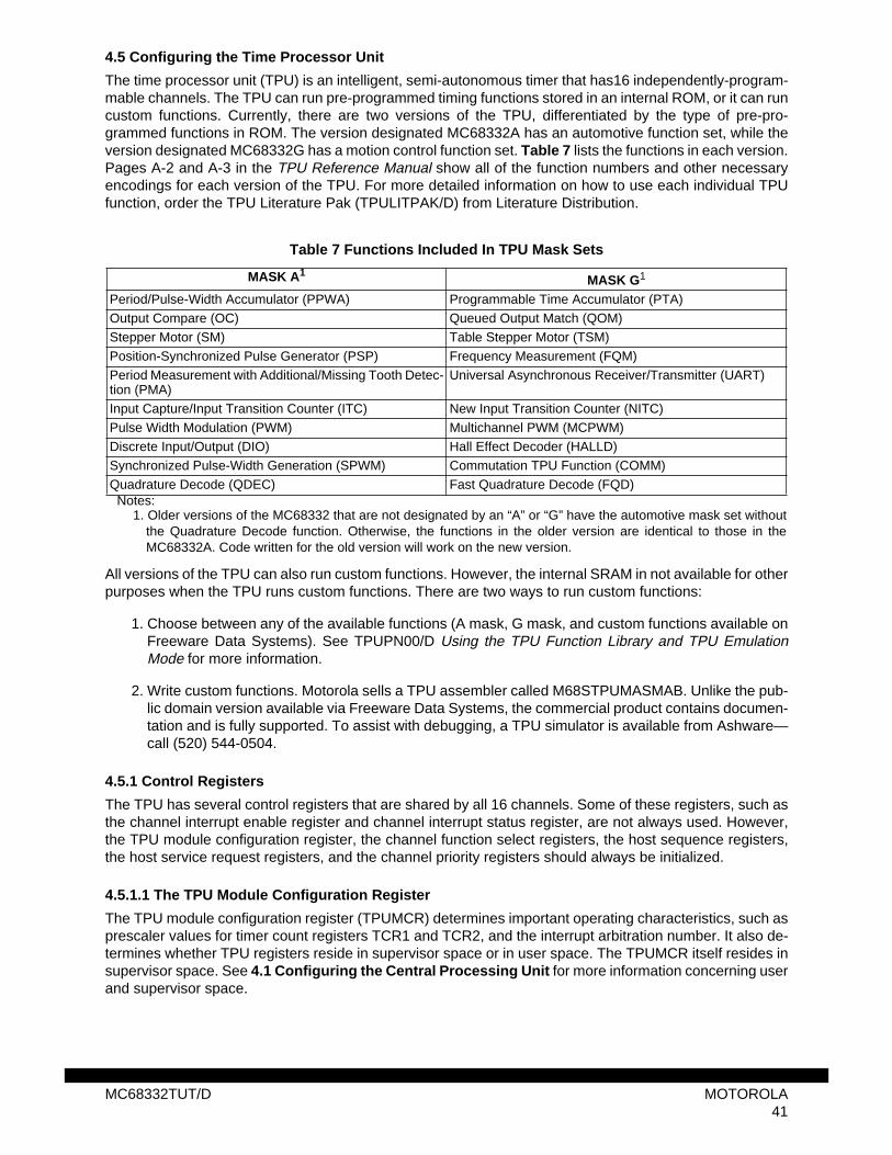
4.5 Configuring the Time Processor Unit
The time processor unit (TPU) is an intelligent, semi-autonomous timer that has16 independently-program-mable channels. The TPU can run pre-programmed timing functions stored in an internal ROM, or it can runcustom functions. Currently, there are two versions of the TPU, differentiated by the type of pre-pro-grammed functions in ROM. The version designated MC68332A has an automotive function set, while theversion designated MC68332G has a motion control function set. Table 7 lists the functions in each version.Pages A-2 and A-3 in the TPU Reference Manual show all of the function numbers and other necessaryencodings for each version of the TPU. For more detailed information on how to use each individual TPUfunction, order the TPU Literature Pak (TPULITPAK/D) from Literature Distribution.
All versions of the TPU can also run custom functions. However, the internal SRAM in not available for otherpurposes when the TPU runs custom functions. There are two ways to run custom functions:
1. Choose between any of the available functions (A mask, G mask, and custom functions available onFreeware Data Systems). See TPUPN00/D Using the TPU Function Library and TPU EmulationMode for more information.
2. Write custom functions. Motorola sells a TPU assembler called M68STPUMASMAB. Unlike the pub-lic domain version available via Freeware Data Systems, the commercial product contains documen-tation and is fully supported. To assist with debugging, a TPU simulator is available from Ashware—call (520) 544-0504.
4.5.1 Control Registers
The TPU has several control registers that are shared by all 16 channels. Some of these registers, such asthe channel interrupt enable register and channel interrupt status register, are not always used. However,the TPU module configuration register, the channel function select registers, the host sequence registers,the host service request registers, and the channel priority registers should always be initialized.
4.5.1.1 The TPU Module Configuration Register
The TPU module configuration register (TPUMCR) determines important operating characteristics, such asprescaler values for timer count registers TCR1 and TCR2, and the interrupt arbitration number. It also de-termines whether TPU registers reside in supervisor space or in user space. The TPUMCR itself resides insupervisor space. See 4.1 Configuring the Central Processing Unit for more information concerning userand supervisor space.
Notes:1. Older versions of the MC68332 that are not designated by an “A” or “G” have the automotive mask set without
the Quadrature Decode function. Otherwise, the functions in the older version are identical to those in theMC68332A. Code written for the old version will work on the new version.
Table 7 Functions Included In TPU Mask Sets
MASK A1MASK G1
Period/Pulse-Width Accumulator (PPWA) Programmable Time Accumulator (PTA)Output Compare (OC) Queued Output Match (QOM)Stepper Motor (SM) Table Stepper Motor (TSM)Position-Synchronized Pulse Generator (PSP) Frequency Measurement (FQM)Period Measurement with Additional/Missing Tooth Detec-tion (PMA)
Universal Asynchronous Receiver/Transmitter (UART)
Input Capture/Input Transition Counter (ITC) New Input Transition Counter (NITC)Pulse Width Modulation (PWM) Multichannel PWM (MCPWM)Discrete Input/Output (DIO) Hall Effect Decoder (HALLD)Synchronized Pulse-Width Generation (SPWM) Commutation TPU Function (COMM)Quadrature Decode (QDEC) Fast Quadrature Decode (FQD)
MC68332TUT/D MOTOROLA41
4.5.1.2 Channel Function Select Registers
Channel function select registers (CFSR[1:3]) contain the function numbers assigned to each individualchannel. These function numbers are mask-set dependent because they are determined by the microcodeassembly.
4.5.1.3 Host Sequence Registers
Host sequence registers (HSQR0 and HSQR1) contain the host sequence bits for the function running ona particular channel. The host sequence bits determine the mode of a particular function. Host sequencebit encoding for each function is determined by microcode, and differs from function to function. For exam-ple, host sequence bits for a function that counts input transitions could determine whether the function op-erates in single-shot mode or continuous mode.
4.5.1.4 Host Service Request Registers
Host servicerequest registers (HSRR0 and HSRR1) contain the service request bits for each channel. Theservice request bits ask the TPU microengine to perform a particular service on the associated channel.Usually, the first service request is for initialization. Another common service request is for an immediateupdate.
Like host sequence bits, host service bit encoding for each function is determined by microcode, and differsfrom function to function. However, the host service bits are different from other control bits because, whilethe CPU can set the service bits, only the TPU can clear them. In fact, the TPU tells the CPU that it hasserviced a channel the first time by clearing the host service request bits. An HSRR should not be writtenunless all of the other parameters and control bits are initialized or the associated channel is disabled (viathe channel priority register) and the host service bits are cleared. The CPU program must wait until a pre-vious service request has been cleared before issuing a new service request.
To make a host service request, follow one of the following scenarios.
1. To initialize a channel out of reset, first initialize the parameter RAM and other control registers, thenmake the host service request for initialization. The final step is to enable the channel via the channelpriority register.
2. To change the function operating on a particular channel, first disable the channel using the channelpriority register, then follow the same steps as for initialization out of reset.
3. To make a host service request other than that for initialization, do not disable the channel. Instead,wait for the TPU to clear the previous host service request. Then, issue a new request. Usually thisis for an immediate update or to force an output state on a particular pin.
To initialize two or more channels that share a host service request register, either write all the fields in theregister at the same time or disable all channels via the channel priority registers, write to the host servicerequest register, then enable each channel as needed via the channel priority registers. This ensures thatconflicts do not occur within the host service request registers. If the channels are running, and cannot bedisabled, write the host service request field for the first channel, then poll those bits until the TPU clearsthem. Then, write the host service request field for the second channel, wait until the TPU clears it, and soon.
4.5.1.5 Channel Priority Registers
The channel priority registers determine how often each channel is serviced. There are three priority levels:high, medium, and low. If the priority bits are set to zero, then a channel is disabled, and the TPU mi-croengine will not service it.
MOTOROLA MC68332TUT/D42
4.5.2 Parameter RAM Registers
Each channel has a dedicated set of word-long registers (called parameters) in the parameter RAM. TPUChannels 0 - 13 have five parameters, and channels 14 and 15 have seven parameters. The CPU and theTPU communicate through the parameter RAM. The meaning of each location in the parameter RAM is de-fined by the microcode for a particular function.
In the TPU manual, addresses in parameter RAM for channels 0 to 13 are defined as $YFFFW0, $YFFFW2,$YFFFW6, $YFFFW8, and $YFFFWA. Channels 14 and 15 have the additional parameters $YFFFWC and$YFFFWE. The “Y” is either an F or a 7, depending on the “MM” bit in the SIM configuration register. Out ofreset, the “Y” is an F. The “W” is the channel number. The last number is the location of the channel param-eters. For example, out of reset, the first parameter for TPU channel 10 is located at $FFFFA0.
TPULITPAK/D contains programming notes for all the A and G mask functions. See the programming notethat pertains to a particular function for a parameter diagram, field encodings, and a description of the op-tions that are available.
4.5.2.1 The Channel Control Register
The channel control register (CCR) is a parameter that is common to most functions. It is nine bits long, andit is usually the first parameter. The CCR allows the CPU to pass information concerning channel configu-ration to the TPU. The microcode for a particular function determines the meaning of data in the CCR. Thefunction may or may not use all of the information, because the microcode can configure the channel withouthelp from the CPU. Usually, the TPU overwrites the CCR after initialization and uses the space for a TPU-controlled parameter.
In general, the channel control register consists of three fields:
1. The time base select (TBS) field determines which timer count register (TCR) the channel uses. Thechannel can match and capture TCR1 and TCR2. The TPU is also capable of matching one TCR andcapturing the other.
2. The pin action control (PAC) field has two basic functions. For an output channel, the PAC field de-termines what type of transition the pin will make when a match occurs. For an input channel, thePAC field determines what type of transition the pin will detect.
3. The pin state control (PSC) field determines initial pin state immediately after a host service request.
See the programming note that pertains to a particular function for specific information about the channelcontrol field.
4.5.3 TPU Interrupts
Several steps must be followed in order for a TPU channel to request interrupt service.
1. Store the starting address of the interrupt service routine in the CPU interrupt vector table.
A. The location in the vector table where the service routine starting address is stored is called thevector address. The vector address is calculated from the interrupt vector number— it is four timesthe vector number plus the value in the vector base register.
B. The interrupt vector number is formed by concatenating a base vector number with the channelnumber. Choose a base vector number and write it to bits 7 through 4 in the TPU interrupt config-uration register (TICR). For example, choosing a base vector number of $80 would assign inter-rupt vector $80 to channel 0, interrupt vector $81 to channel 1, interrupt vector $82 to channel 2,and so on, through assignment of interrupt vector $8F to channel 15.
For example, if channel 4 is being set up to request interrupt service, the interrupt vector is $84.Assuming the vector baseregister holds a value of zero, the vector address is:
MC68332TUT/D MOTOROLA43
4 ∗ $84 + $00 = $210
Thus, the starting address of the interrupt routine must be stored in location $210.
2. Store an interrupt priority level for the TPU in bits 10 through 8 of the TICR.
A. This value determines the priority of TPU interrupt service requests. The value must be a numberbetween 1 and 7— level 7 has the highest priority, and level 1 has the lowest. The value storedin the IPL field in the CPU status register determines whether an interrupt request is recognized.The value in the IPL field must be lower than the TPU interrupt priority level in order for the TPUto interrupt the CPU, unless the interrupt level is seven, in which case it cannot be masked.
3. Store an interrupt arbitration value in the IARB field of the TPU module configuration register.
A. The IARB field value determines precedence when the CPU receives more than one interrupt re-quest of the same interrupt priority level. Each interrupting module must be assigned a uniqueIARB number between $01 (lowest precedence) and $0F (highest precedence).
4. Set the interrupt enable bit for the channel in the channel interrupt enable register (CIER). This simplyinvolves writing the channel's bit number to a one.
To clear an interrupt, negate the appropriate interrupt status flag in the channel interrupt status register(CISR). Read the flag in the asserted state and then write a zero to the bit. As long as the CISR bit is set,the channel will continue to request interrupts.
4.5.4 TPU Initialization Examples
The following example initializes channel 0 to run the PWM function. The output of channel 0 will be a 50%duty cycle square wave. The frequency will be (SYSCLK/4)/$4000. For 16.778 MHz, this is (4194500/16384) = 256 Hz. It assumes that the “MM” bit in the SIMCR is set to a one.
SYNCR EQU $FFFA04SYPCR EQU $FFFA21CFSR3 EQU $FFFE12TPUMCR EQU $FFFE00HSQR1 EQU $FFFE16HSSR1 EQU $FFFE1ACPR1 EQU $FFFE1E
ORG $400 ;begin program at $400, immediately ;after the exception table
INITSYS:
MOVE.B #$7F,(SYNCR).L ;set system clock to 16.78 MHz CLR.B (SYPCR).L ;disable software watchdogCNTLREG: MOVE.W #$0009,(CFSR3).L ;channel function select field. Note: ;function numbers may vary with differ- ;ent mask sets. MOVE.W #$00C0,(TPUMCR).L ;set TCR1 to SYSCLK/4. At 16.778 MHz, ;this means that 1 TCR1 count = 238nsec. MOVE.W #$0000,(HSQR1).L ;HSQ bits = 0 for PWM functionPRAM: MOVE.W #$0092,($FFFF00).L ;Channel Control Reg: Force pin low at ;initialization, use TCR1 MOVE.W #$2000,($FFFF04).L ;High time = $2000 TCR1 counts MOVE.W #$4000,($FFFF06).L ;Period = $4000 TCR1 countsSTART: MOVE.W #$0002,(HSSR1).L ;Host service request for initialization MOVE.W #$0003,(CPR1).L ;Give channel high priorityDONE BRA DONE
Following is a short example that generates interrupts on Channel 4:
MOTOROLA MC68332TUT/D44
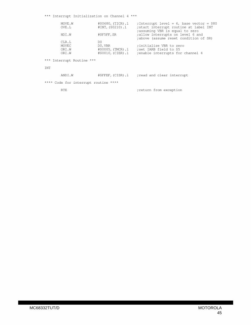
*** Interrupt Initialization on Channel 4 ***
MOVE.W #$0680,(TICR).l ;Interrupt level = 6, base vector = $80 OVE.L #INT,($0210).l ;start interrupt routine at label INT ;assuming VBR is equal to zero NDI.W #$F5FF,SR ;allow interrupts on level 6 and ;above (assume reset condition of SR) CLR.L D0 MOVEC D0,VBR ;initialize VBR to zero ORI.W #$0005,(TMCR).l ;set IARB field to $5 ORI.W #$0010,(CIER).l ;enable interrupts for channel 4
*** Interrupt Routine ***
INT
ANDI.W #$FFEF,(CISR).l ;read and clear interrupt
**** Code for interrupt routine ****
RTE ;return from exception
MC68332TUT/D MOTOROLA45
5 TROUBLESHOOTINGBecause of the complexity of the MCU, there are a considerable number of potential ‘fatal flaws’ that cancause a prototype application to either not operate from power up, or to fail soon after. This section coverscommon problems, causes, and fixes.This is not an exhaustive discussion, but is intended to be used as acheck list of the main problem areas that can cause an application to fail.
5.1 Critical Signals to Check
• RESET should stay low for at least 512 clocks during a power-on reset. If using the internal PLL,RESET will remain low for a little longer because the VCO must lock first. RESET should then go highand remain high.
• CLKOUT should be at the system clock frequency. If MODLCK is held high at the release of reset,CLKOUT should be 512 times the frequency going into EXTAL (8.389 MHz for a 32.768 kHz crystal).Make sure that the frequency is exact, as a measurable error may indicate limp mode and oscillatorfaults. If MODCLK is held low at the release of reset, the frequency on CLKOUT should be the fre-quency going into EXTAL.
• Immediately after reset, CSBOOT should pulse low five times for a 16-bit port and nine times for an8-bit port.
• FREEZE should be low and HALT should be high. Otherwise, the MCU is halted, or is in BDM.
• BR and BGACK should be high. Otherwise, the external bus is granted away.
• Make sure that the data bus pins are configured correctly during reset.
• Make sure that IRQ7 is high during reset.
5.2 Common Problems and Solutions
5.2.1 Problem: Device Stays in Reset
1. There is no pull-up resistor on RESET. RESET needs an 820 Ω resistor to 5 volts. See 2.1 UsingData Bus Pins to Configure the MCU and 2.3 Pins that Need Pull-Up Resistors.
2. A capacitor on RESET can also prevent the device from coming out of reset. Do not put any capac-itors on RESET. See Sections 2.1 and 2.3.
3. MODCLK is pulled high at the release of RESET, and the VCO is not locking. Check the componentsin the crystal circuit to ensure that they are correct. Check the layout to ensure that the board is cleanand that there are no noisy signals nearby to affect operation of the oscillator, and make sure thatpower is applied to VDDSYN. Also, make sure that the crystal frequency is within specifications. If allelse fails, change crystals. See 2.5 Clock Circuitry.
4. MODCLK is pulled low at the release of RESET, and there is no external clock signal. Make sure thatthere is a signal going into EXTAL. See 2.5 Clock Circuitry.
5.2.2 Problem: Device Resets Every 16 ms
1. The software watchdog is enabled but is not being serviced by the program. When the watchdog isenabled, the program must write a sequence to the software service register to prevent the watchdogfrom timing out and resetting the MCU. The software watchdog is enabled out of reset, and the pro-gram must disable it by clearing the SWE bit in the SYPCR register. Note that this is a write-once onlyregister.
MOTOROLA MC68332TUT/D46
2. If the code does disable the watchdog, but the device is still resetting every 16 ms, then the code isprobably not being executed. Either the memory is not programmed properly, or something is pre-venting the MCU from executing code. Check all pull-up resistors for good connections and correctvalues. Also check the frequency of CLKOUT.
5.2.3 Problem: CLKOUT Frequency is Incorrect
1. MODCLK is not driven correctly during reset. To use a crystal and the internal PLL, MODCLK mustbe driven high during reset. To use an external clock and bypass the internal PLL, MODCLK must bedriven low during reset.
2. The crystal is settling into overtones due to a poor quality crystal or incorrect components in the crys-tal circuit.
3. If the frequency is unstable, it is possible that the crystal is being overdriven. Increase Rs to reducecrystal drive.
4. There is residue on the PCB. Since low frequency crystal circuits tend to be very high impedance,the PCB must be clean, dry, and free of conductive material such as solder rosin and excessive mois-ture from high humidity.
5. In the absence of other circuit problems, the series resistor is the most probable culprit when an os-cillator will not start. The resistor limits the power that starts the crystal oscillating. If the resistance istoo low, the crystal will start oscillating in unpredictable modes and could even become damaged. Ifthe resistance is too high, the oscillator will start very slowly or not at all.
6. If the value of the series resistor is correct, check for the presence of metastable states during power-up. If there is extremely high frequency oscillation on the CLKOUT pin during the first few hundredmilliseconds of operation, and increasing the size of Rs does not fix the problem, the only real solutionis to find a different brand and/or style of crystal. There is no practical way to compensate for a crystalthat exhibits poor self-suppression of the first overtone and first harmonic. Once again, if a particularcrystal type and brand is prone to starting at overtones or harmonics, just don’t use it. No amount ofcircuit design will ever compensate for a bad or poor quality crystal.
Usually, it is impossible to observe oscillator operation with an oscilloscope connected to one of the oscil-lator pins. The oscilloscope adds 3-30 pF and 1-10 MΩ of loading to VSS, which will usually affect oscillatoroperation. When the oscilloscope is connected to the EXTAL input, the 10 MΩ to VSS (oscilloscope input)forms a resistive divider with Rf and often disables the oscillator by biasing the circuit out of the linear regionof the EXTAL input. This problem can sometimes be overcome by capacitively coupling the oscilloscopewith a very small capacitor (1-5 pF) between the oscilloscope probe and the oscillator pin.
It is better to observe the CLKOUT signal, since this does not alter the operation of the oscillator. It may bepossible to observe XTAL since it is isolated from rest of oscillator by Rs. Observe IDD without oscilloscopeconnected and again with it connected. If IDD is unchanged, it is usually safe to assume the oscillator wasunaffected. For additional information, see 2.5 Clock Circuitry.
5.2.4 Problem: System Crashes after Fetching Reset Vector
1. Incorrect reset configuration of boot memory width is causing the address bus to increment by thewrong amount during fetches of the reset vectors. Check DATA0 to make sure that it is being drivento the correct state during reset. If CSBOOT is a 16-bit port, drive DATA0 high during reset; if it is an8-bit port, drive DATA0 low. See 2.1 Using Data Bus Pins to Configure the MCU.
2. An IRQ7 interrupt is received during or immediately after reset. The MCU will recognize the interruptafter fetching the reset information and first instruction. In a typical system that is booting out of ROM,stack RAM will not be enabled at this point, and the first bus cycle to write the stack frame will hangthe MCU. Make sure that the IRQ[7:1] lines are either pulled up through resistors to 5 volts or config-ure the pins as PORTF I/O lines by pulling DATA9 low during reset. Also, start-up software shouldenable the stack RAM (by configuring the appropriate chip-select circuits) before enabling the inter-
MC68332TUT/D MOTOROLA47
rupt lines (by writing to the PFPAR register). This problem is likely to be intermittent, as it would onlyoccur if an IRQ7 interrupt is received in the short time before system initialization. See 2.1 UsingData Bus Pins to Configure the MCU.
3. An interrupt is received, and the interrupt vectors have not been initialized. Make sure that the inter-rupt vectors are initialized. See 4.1.3.2 Initializing Exception Vectors other than Reset.
4. The BR or BGACK pin has floated low and the CPU has relinquished control of the bus. Configurethese pins for chip-select operation out of reset by pulling DATA1 high during reset, or put pull-upresistors on these pins.
5. Some of the pins are being powered up before VDD. If the MCU is connected to another system witha separate power supply, use an LVI device to prevent the system with the faster power supply fromdriving logic one levels before the system with the slower power supply has become operational. Ifthis happens, the driven pins on the device with the slow supply will momentarily have a higher volt-age than the VDD pin. This condition can cause the input protection diodes to become momentarilyforward biased and cause significant current injection into the device substrate, which will probablyimproperly charge or discharge some of the internal nodes of the MCU. This action is completely ran-dom, and it is impossible to predict what will happen when significant injection occurs. Usually, theMCU will not function at all and will display undefined states. For example, the RESET, HALT, BERR,BR and FREEZE signals may be asserted but the device may fail to fetch opcodes. See 2.7 PowerSupply.
5.2.5 Problem: Debug System Cannot Enter BDM
1. BKPT is not held low at the release of RESET. Holding BKPT low at the release of RESET enablesBDM, and driving it low after reset causes the processor to enter BDM. The debugger should takecare of this.
2. The memory is uninitialized, and the processor is trying to access bad addresses. In this case, mostdebuggers should drive BERR to terminate the bus cycle. If the debugger does not do this, eitherwrite valid addresses to the reset vectors or, if this is not possible, manually pulse BERR low to ter-minate a hung bus cycle.
5.2.6 Problem: The Processor Takes a Spurious Interrupt Exception
1. The interrupt arbitration (IARB) field for the module requesting interrupt service is not a unique, non-zero value. Each internal module has its own IARB field. External interrupts use the IARB field in theSIMCR interrupts.
2. There are noise spikes on an IRQ line. Use pull-up resistors on the IRQ lines.
3. A square wave is used to generate external interrupts, and the source of the interrupt is going awaybefore the interrupt is acknowledged.
4. The program code is disabling an internal module or is using the BCLR instruction to arbitrarily clearinterrupt enable bits for an internal module before the interrupt is acknowledged. Instead of arbitrarilyclearing the enable bits, first mask out the interrupt level by writing to the IPL field in the CPU statusregister. For example, if a level 3 interrupt is to be masked, set the IPL field to 3 or higher. Then, dis-able the enable bit for the specific interrupt.
5. An internal module is initialized improperly in such a way that the module cannot respond with aninternal DSACK even when that module is the one asserting the interrupt.
6. The IACK cycle is terminated by BERR instead of DSACK or AVEC. The assertion of BERR causesthe spurious interrupt vector (vector number 24) to be taken. A spurious interrupt will be taken in thefollowing three situations:
MOTOROLA MC68332TUT/D48
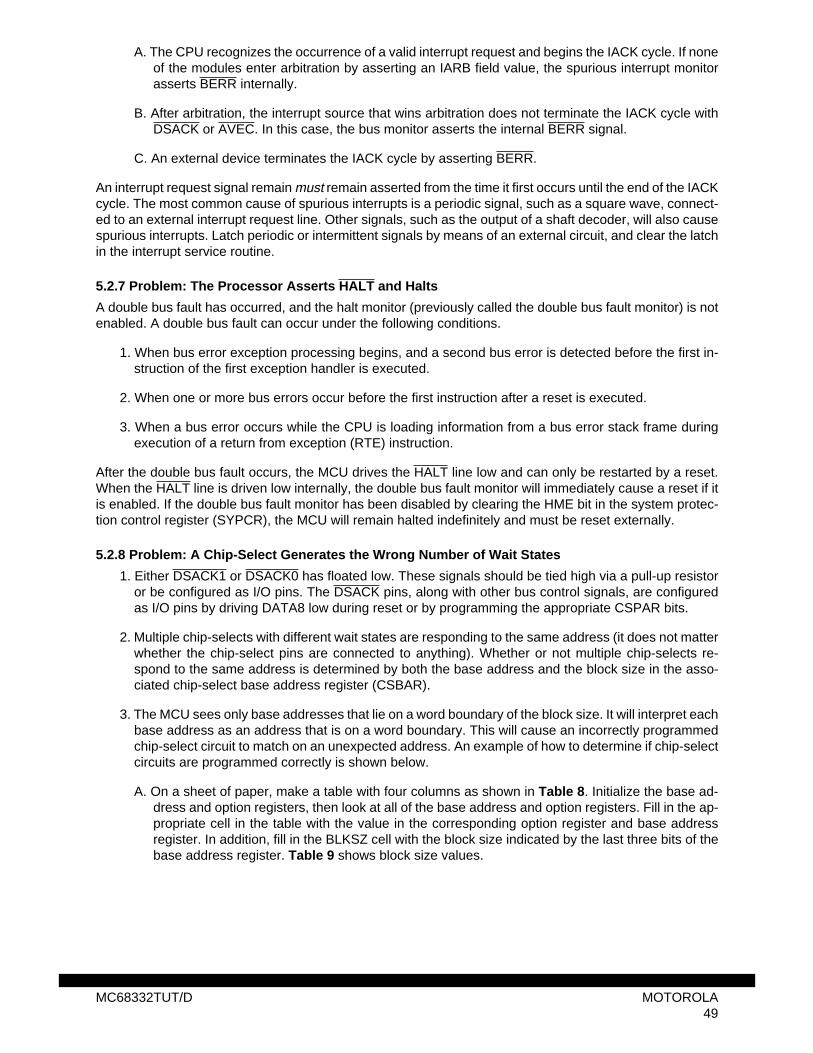
A. The CPU recognizes the occurrence of a valid interrupt request and begins the IACK cycle. If noneof the modules enter arbitration by asserting an IARB field value, the spurious interrupt monitorasserts BERR internally.
B. After arbitration, the interrupt source that wins arbitration does not terminate the IACK cycle withDSACK or AVEC. In this case, the bus monitor asserts the internal BERR signal.
C. An external device terminates the IACK cycle by asserting BERR.
An interrupt request signal remain must remain asserted from the time it first occurs until the end of the IACKcycle. The most common cause of spurious interrupts is a periodic signal, such as a square wave, connect-ed to an external interrupt request line. Other signals, such as the output of a shaft decoder, will also causespurious interrupts. Latch periodic or intermittent signals by means of an external circuit, and clear the latchin the interrupt service routine.
5.2.7 Problem: The Processor Asserts HALT and Halts
A double bus fault has occurred, and the halt monitor (previously called the double bus fault monitor) is notenabled. A double bus fault can occur under the following conditions.
1. When bus error exception processing begins, and a second bus error is detected before the first in-struction of the first exception handler is executed.
2. When one or more bus errors occur before the first instruction after a reset is executed.
3. When a bus error occurs while the CPU is loading information from a bus error stack frame duringexecution of a return from exception (RTE) instruction.
After the double bus fault occurs, the MCU drives the HALT line low and can only be restarted by a reset.When the HALT line is driven low internally, the double bus fault monitor will immediately cause a reset if itis enabled. If the double bus fault monitor has been disabled by clearing the HME bit in the system protec-tion control register (SYPCR), the MCU will remain halted indefinitely and must be reset externally.
5.2.8 Problem: A Chip-Select Generates the Wrong Number of Wait States
1. Either DSACK1 or DSACK0 has floated low. These signals should be tied high via a pull-up resistoror be configured as I/O pins. The DSACK pins, along with other bus control signals, are configuredas I/O pins by driving DATA8 low during reset or by programming the appropriate CSPAR bits.
2. Multiple chip-selects with different wait states are responding to the same address (it does not matterwhether the chip-select pins are connected to anything). Whether or not multiple chip-selects re-spond to the same address is determined by both the base address and the block size in the asso-ciated chip-select base address register (CSBAR).
3. The MCU sees only base addresses that lie on a word boundary of the block size. It will interpret eachbase address as an address that is on a word boundary. This will cause an incorrectly programmedchip-select circuit to match on an unexpected address. An example of how to determine if chip-selectcircuits are programmed correctly is shown below.
A. On a sheet of paper, make a table with four columns as shown in Table 8. Initialize the base ad-dress and option registers, then look at all of the base address and option registers. Fill in the ap-propriate cell in the table with the value in the corresponding option register and base addressregister. In addition, fill in the BLKSZ cell with the block size indicated by the last three bits of thebase address register. Table 9 shows block size values.
MC68332TUT/D MOTOROLA49
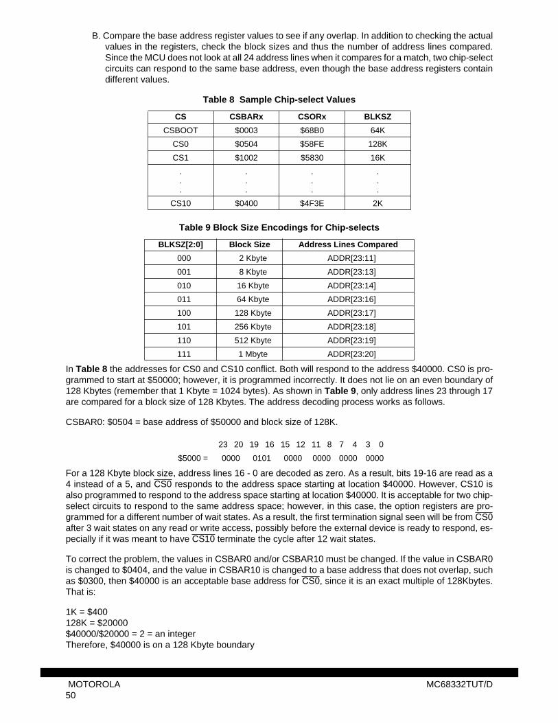
B. Compare the base address register values to see if any overlap. In addition to checking the actualvalues in the registers, check the block sizes and thus the number of address lines compared.Since the MCU does not look at all 24 address lines when it compares for a match, two chip-selectcircuits can respond to the same base address, even though the base address registers containdifferent values.
In Table 8 the addresses for CS0 and CS10 conflict. Both will respond to the address $40000. CS0 is pro-grammed to start at $50000; however, it is programmed incorrectly. It does not lie on an even boundary of128 Kbytes (remember that 1 Kbyte = 1024 bytes). As shown in Table 9, only address lines 23 through 17are compared for a block size of 128 Kbytes. The address decoding process works as follows.
CSBAR0: $0504 = base address of $50000 and block size of 128K.
For a 128 Kbyte block size, address lines 16 - 0 are decoded as zero. As a result, bits 19-16 are read as a4 instead of a 5, and CS0 responds to the address space starting at location $40000. However, CS10 isalso programmed to respond to the address space starting at location $40000. It is acceptable for two chip-select circuits to respond to the same address space; however, in this case, the option registers are pro-grammed for a different number of wait states. As a result, the first termination signal seen will be from CS0after 3 wait states on any read or write access, possibly before the external device is ready to respond, es-pecially if it was meant to have CS10 terminate the cycle after 12 wait states.
To correct the problem, the values in CSBAR0 and/or CSBAR10 must be changed. If the value in CSBAR0is changed to $0404, and the value in CSBAR10 is changed to a base address that does not overlap, suchas $0300, then $40000 is an acceptable base address for CS0, since it is an exact multiple of 128Kbytes.That is:
1K = $400128K = $20000$40000/$20000 = 2 = an integerTherefore, $40000 is on a 128 Kbyte boundary
Table 8 Sample Chip-select Values
CS CSBARx CSORx BLKSZ
CSBOOT $0003 $68B0 64K
CS0 $0504 $58FE 128K
CS1 $1002 $5830 16K
.
.
.
.
.
.
.
.
.
.
.
.
CS10 $0400 $4F3E 2K
Table 9 Block Size Encodings for Chip-selects
BLKSZ[2:0] Block Size Address Lines Compared
000 2 Kbyte ADDR[23:11]
001 8 Kbyte ADDR[23:13]
010 16 Kbyte ADDR[23:14]
011 64 Kbyte ADDR[23:16]
100 128 Kbyte ADDR[23:17]
101 256 Kbyte ADDR[23:18]
110 512 Kbyte ADDR[23:19]
111 1 Mbyte ADDR[23:20]
23 20 19 16 15 12 11 8 7 4 3 0
$5000 = 0000 0101 0000 0000 0000 0000
MOTOROLA MC68332TUT/D50
6 SOURCES OF INFORMATION
6.1 Technical Literature
All Motorola literature can be ordered by mail from Motorola Literature Distribution Centers (shown on theback page of this publication) or through local sales offices. For U.S. and European literature orders, call(800) 441-2447. Motorola publication BR1116/D, Advanced Microcontroller Technical Literature, includes acomplete listing of literature, sales offices, distributors, and an order form.
6.1.1 User’s Manual
MC68332 User’s Manual (MC68332UM/AD)
6.1.2 Reference Manuals
M68300 Family CPU32 Central Processor Unit Reference Manual (CPU32RM/AD).
Modular Microcontroller Family Queued Serial Module Reference Manual (QSMRM/AD).
Modular Microcontroller Family System Integration Module Reference Manual (SIMRM/AD).
Modular Microcontroller Family Time Processor Unit Reference Manual (TPURM/AD).
6.1.3 Application Notes
AN437/D Using the MC68332 Periodic Interrupt Timer
AN473/D A Minimum Evaluation System for 331 & 332
AN455/D Using the Table Interpolation Features of the CPU32
AN1050/D Designing for Electromagnetic Compatibility with HCMOS Microcontrollers
AN1051/D Transmission Line Effects in PCB Applications
AN1310/D Using the MC68332 Microcontroller for AC Induction Motor Control
AN1062/D Using the QSPI for Analog Data Acquisition
AN1200/D Configuring the M68300 Family TPU
AN1230/D A BDM Driver Package for Modular Microcontrollers
AN1236/D Timing Performance of TPU I/O Hardware.
AN1063/D DRAM controller for the MC68340
6.1.4 TPU Programming Notes
TPUPN00/D Using the TPU Function Library and TPU Emulation Mode
TPUPN01/D Queued Output Match TPU Function (QOM)
TPUPN02/D Fast Quadrature Decode TPU Function (FQD)
TPUPN03/D Frequency Measurement TPU Function (FQM)
TPUPN04/D Table Stepper Motor TPU Function (TSM)
TPUPN05/D Multichannel PWM TPU Function (MCPWM)
TPUPN06/D Pulse and Transition Accumulate TPU Function (PTA)
TPUPN07/D Universal Asynchronous Receiver/Transmitter (UART)
TPUPN08/D New Input Transition Capture TPU Function (NITC)
TPUPN09/D Commutation TPU Function (COMM)
TPUPN10/D Hall Effect Decode TPU Function (HALLD)
TPUPN11/D Period Pulse Width Accumulate TPU Function (PPWA)
TPUPN12/D Output Compare TPU Function (OC)
MC68332TUT/D MOTOROLA51
TPUPN13/D Stepper Motor TPU Function (SM)
TPUPN14/D Position Synchronized Pulse Generator TPU Function (PSP)
TPUPN15A/D Period Measurement with Additional Transition (PMA)
TPUPN15B/D Period Measurement with Missing Transition TPU Function (PMM)
TPUPN16/D Input Transition Capture TPU Function (ITC)
TPUPN17/D Pulse Width Modulation TPU Function (PWM)
TPUPN18/D Discrete I/O TPU Function (DIO)
TPUPN19/D Synchronized Pulse Width Modulation TPU Function (SPWM)
TPUPN20/D Quadrature Decode TPU Function (QDEC)
The TPU Literature Package (TPULITPAK/D) includes the TPU Reference Manual and a complete setof programming notes:
6.1.5 Development Tools and Software
Motorola Microcontroller Development Tools Directory (MCUDEVTLDIR/D Rev. 2).
6.1.6 Books
The Motorola MC68332 Microcontroller (TB325/D).
Programming Microcontrollers in C (TB328)
6.2 Freeware Data Systems
The Motorola Freeware BBS can be accessed by modem at phone number is (512) 891-3733. Freewarecan be accessed via internet at freeware.aus.sps.mot.com. For World Wide Web access, use http://free-ware.aus.sps.mot.com/. The Freeware system contains a wealth of information concerning Motorola MCUsand downloadable software.
6.2.1 Application Snapshots
Application snapshots provide brief discussions of commonly-encountered problems and technical issuesconcerning MCUs. Snapshots are available on the Freeware system — access the Tech_Notes area to seea list of topics and download snapshots. The system provides instructions concerning navigation and down-loading files.
6.3 Other Sources
“EDN Magazine’s Designer’s Guide to Electromagnetic Compatibility.” Call (800) 523-9654 for a reprintof the article.
EITD Electronic Industry Telephone Directory. Lists phone numbers, addresses, and fax numbers ofabout 30,000 sources for electronics products and services. Call (800) 888-5900 or (216) 425-9000.
MOTOROLA MC68332TUT/D52

MC68332TUT/D MOTOROLA53

MOTOROLA MC68332TUT/D54

MC68332TUT/D MOTOROLA55
Motorola uitabilityof its pro any andall liabilit cluding"Typicals f others.Motorola nded tosupport o d Buyerpurchase idiaries,affiliates, ersonalinjury or e part. MOTOR
reserves the right to make changes without further notice to any products herein. Motorola makes no warranty, representation or guarantee regarding the sducts for any particular purpose, nor does Motorola assume any liability arising out of the application or use of any product or circuit, and specifically disclaims y, including without limitation consequential or incidental damages. "Typical" parameters can and do vary in different applications. All operating parameters, in" must be validated for each customer application by customer's technical experts. Motorola does not convey any license under its patent rights nor the rights o products are not designed, intended, or authorized for use as components in systems intended for surgical implant into the body, or other applications inter sustain life, or for any other application in which the failure of the Motorola product could create a situation where personal injury or death may occur. Shoul or use Motorola products for any such unintended or unauthorized application, Buyer shall indemnify and hold Motorola and its officers, employees, subs and distributors harmless against all claims, costs, damages, and expenses, and reasonable attorney fees arising out of, directly or indirectly, any claim of pdeath associated with such unintended or unauthorized use, even if such claim alleges that Motorola was negligent regarding the design or manufacture of thOLA and ! are registered trademarks of Motorola, Inc. Motorola, Inc. is an Equal Opportunity/Affirmative Action Employer.
How to reach us:USA/EUROPE: Motorola Literature Distribution; P.O. Box 20912; Phoenix, Arizona 85036. 1-800-441-2447MFAX: [email protected] - TOUCHTONE (602) 244-6609INTERNET: http://Design-NET.comJAPAN: Nippon Motorola Ltd.; Tatsumi-SPD-JLDC, Toshikatsu Otsuki, 6F Seibu-Butsuryu-Center, 3-14-2 Tatsumi Koto-Ku, Tokyo 135, Japan. 03-3521-8315HONG KONG: Motorola Semiconductors H.K. Ltd.; 8B Tai Ping Industrial Park, 51 Ting Kok Road, Tai Po, N.T., Hong Kong. 852-26629298