Embed Size (px)
Citation preview
AN10993 Pegoda Software Design Guide Rev. 2.1 — 08 August 2012 196121
Application note COMPANY PUBLIC
Document information Info Content Keywords Pegoda software design guide, firmware documentation, software
documentation, firmware update, Pegoda firmware architecture, Pegoda functional overview, PC/SC mode
Abstract This document provides a comprehensive architectural overview of the Pegoda software.
NXP Semiconductors AN10993 Pegoda Software Design Guide
AN10993 All information provided in this document is subject to legal disclaimers. © NXP B.V. 2012. All rights reserved.
Application note COMPANY PUBLIC
Rev. 2.1 — 08 August 2012 196121
2 of 53
Contact information For more information, please visit: http://www.nxp.com
For sales office addresses, please send an email to: [email protected]
Revision history Rev Date Description 2.1 20120808 References updated
2.0 20120716 General update for new firmware (v2.2.7)
1.0 20101101 First release

NXP Semiconductors AN10993 Pegoda Software Design Guide
AN10993 All information provided in this document is subject to legal disclaimers. © NXP B.V. 2012. All rights reserved.
Application note COMPANY PUBLIC
Rev. 2.1 — 08 August 2012 196121
3 of 53
1. Introduction
1.1 Scope The scope of this document covers the software architecture coming with the Pegoda package. This includes a description of the integrated firmware stack on the LPC1768 controller as well as a high level overview of available modes in RD710.
The NPX Reader Library (nxprdlib) architecture and modules are covered in a separate document [10].
The firmware\nxprdlib may be changed individually to its own needs. An adequate tool chain for loading the firmware project file and doing further programming/debugging is introduced in the documents [7].
This document primarily describes the latest firmware release (V2.2.7) but for historical reasons a description of the old firmware is added as well in the Appendix in section 5.
Updates for the latest or for future firmware releases may be provided by NXP and can be easily downloaded by USB as described in [9].
Fig 1. Flowchart
Pegoda Reader
RD710
Reader Firmware
on LPC1768
Software Design
Guide
AN10993
PC/HOST
Reader library and
examples running
.NET
Example Project
AN10990
MIFARE
Discover
or any
PC/SC SW
Quick Start
Guide
AN10992
Legend
Software and Tools
Application Notes
Toolchain
Loading Firmware
Programming and
Debugging
Pegoda
Toolchains
AN11002

NXP Semiconductors AN10993 Pegoda Software Design Guide
AN10993 All information provided in this document is subject to legal disclaimers. © NXP B.V. 2012. All rights reserved.
Application note COMPANY PUBLIC
Rev. 2.1 — 08 August 2012 196121
4 of 53
1.2 Audience This document is intended for use by manufacturers wanting to develop applications based on the software stack delivered within the Pegoda package.
Note that understanding parts of this document requires knowledge on microcontroller and their underlying systems.
1.3 Applicable documents or references [1] [ISO/IEC 14443]
[2] PC/SC Workgroup Specifications (www.nxp.com/redirect/pcscworkgroup.com/specifications/specdownload)
[3] onARM: see www.nxp.com/redirect/onarm for more information
[4] See www.nxp.com/redirect/freetos for more information
[5] www.nxp.com/redirect/en.wikipedia.org/wiki/Interrupt_handler
[6] AN10990 Example Project Pegoda
[7] AN11002 Pegoda Toolchain Information
[8] www.nxp.com/redirect/ics.nxp.com/products/lpc1000/all/~LPC1768 or on CD
[9] AN10992 Quick start up guide
[10] NXP Reader Library (in .chm format in the source code on CD include)
For information on availability of samples as well as documentation, please refer to the application note ‘AN10994 Pegoda EV710 Documentation and Sampling guide’.
1.4 Acronyms and abbreviations SAM Secure Access Module
S SAM in S-Mode
N no SAM
X SAM in X-Mode
BFL Basic Function Library
NXP Semiconductors AN10993 Pegoda Software Design Guide
AN10993 All information provided in this document is subject to legal disclaimers. © NXP B.V. 2012. All rights reserved.
Application note COMPANY PUBLIC
Rev. 2.1 — 08 August 2012 196121
5 of 53
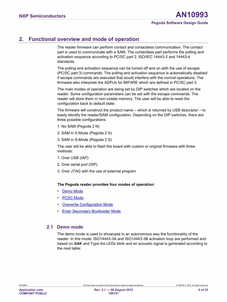
2. Functional overview and mode of operation The reader firmware can perform contact and contactless communication. The contact part is used to communicate with a SAM. The contactless part performs the polling and activation sequence according to PC/SC part 2, ISO/IEC 14443-3 and 14443-4 standards.
The polling and activation sequence can be turned off and on with the use of escape (PC/SC part 3) commands. The polling and activation sequence is automatically disabled if escape commands are executed that would interfere with the normal operations. The firmware also interprets the ADPUs for MIFARE which are defined in PC/SC part 3.
The main modes of operation are being set by DIP switches which are located on the reader. Some configuration parameters can be set with the escape commands. The reader will store them in non-violate memory. The user will be able to reset the configuration back to default state.
The firmware will construct the product name – which is returned by USB descriptor – to easily identify the reader/SAM configuration. Depending on the DIP switches, there are three possible configurations
1. No SAM (Pegoda 2 N)
2. SAM in X-Mode (Pegoda 2 X)
3. SAM in S-Mode (Pegoda 2 S)
The user will be able to flash the board with custom or original firmware with three methods:
1. Over USB (IAP)
2. Over serial port (ISP)
3. Over JTAG with the use of external program
The Pegoda reader provides four modes of operation:
• Demo Mode
• PCSC Mode
• Overwrite Configuration Mode
• Enter Secondary Bootloader Mode
2.1 Demo mode The demo mode is used to showcase in an autonomous way the functionality of the reader. In this mode, ISO14443-3A and ISO14443-3B activation loop are performed and based on SAK and Type the LEDs blink and an acoustic signal is generated according to the next table:

NXP Semiconductors AN10993 Pegoda Software Design Guide
AN10993 All information provided in this document is subject to legal disclaimers. © NXP B.V. 2012. All rights reserved.
Application note COMPANY PUBLIC
Rev. 2.1 — 08 August 2012 196121
6 of 53
Table 1. Card type according to SAK and number of beeps and lights Card type sound blink MIFARE 1K (0x08) 1 2
MIFARE Classic 4K (0x18) 2 2
MIFARE Ultralight (0x00) 3 2
MIFARE DESFire 4 2
MIFARE Plus 5 2
ISO14443 Type B 1 1
The demo mode is implemented in src/ p3fw_demo.c in the task:
void p3fw_task_demo_mode (void * param );
Demo mode firstly performs initialization of NXPRdLib and then enters the activation loop.
2.2 PC/SC Mode For PCSC Mode to function we first need to setup card slots and prepare NXPRdLib protocol stacks with:
void p3fw_slots_init(void);
which can be found in src/p3fw_slots.c. Next we set up external communication interface as USB, with the help of:
void p3fw_ext_if_init_usb(void);
Now we can start the two main tasks which perform all the necessary work:
Card Poll and Activation Task PCSC Execute Task
As ther are three types of operating modes within the PC/SC mode:
No SAM mode
SAM in non X-mode
SAM in X-Mode We must decide which is required because if we use Pegoda in SAM-X mode then we do not need the Card Poll and Activation task.
2.2.1 No SAM mode The most important aspect of this mode is performing activation and polling sequence for ISO 14443 A type cards as defined in PC/SC part 3. Selected cards are put in slot manager and notification is sent to PC/SC driver. There can be only one ISO 14443-3 card or multiple (maximum 14) ISO 14443-4 cards in the field.

NXP Semiconductors AN10993 Pegoda Software Design Guide
AN10993 All information provided in this document is subject to legal disclaimers. © NXP B.V. 2012. All rights reserved.
Application note COMPANY PUBLIC
Rev. 2.1 — 08 August 2012 196121
7 of 53
Fig 2. No SAM configuration
2.2.2 SAM in non X-mode SAM in non X-mode is similar as 2.2.1 No SAM mode. The only difference is that slot 0 is always occupied with SAM, which can be used as key store, cryptographic engine, etc.
The reader chip can not be controlled by SAM in this mode.
Fig 3. SAM in non X configuration
2.2.3 SAM in X-mode In this mode communication is only through SAM (slot 0). Only limited number of proprietary commands can be executed.

NXP Semiconductors AN10993 Pegoda Software Design Guide
AN10993 All information provided in this document is subject to legal disclaimers. © NXP B.V. 2012. All rights reserved.
Application note COMPANY PUBLIC
Rev. 2.1 — 08 August 2012 196121
8 of 53
Fig 4. SAM in X-mode configuration
2.2.4 Card Poll and Activation Task Card Poll and Activation Task checks if there is an empty slot and if one exists, it tries to activate a new card. After a card (or cards – depends on the card and reader configuration) is activated and added to previously empty slot, it regularly checks if the card is still present. Task is implemented in function:
void p3fw_task_poll_and_activate(void * param); in src/p3fw_poll.c file, as also all the bellow functions. Card activation (for ISO14443-3A, ISO14443-3B and ISO14443-4 cards) happens in:
void p3fw_check_for_new_card(uint8_t bCLSlotIndex);
This checks if there is any new card available and puts it in a card slot numbered by bCLSlotIndex. Presence check is performed by:
for ISO14443-3A cards: void p3fw_check_presence_l3a_card(uint8_t bCLSlotIndex);
for ISO14443-3B cards: void p3fw_check_presence_l3b_card(uint8_t bCLSlotIndex);
for ISO14443-4 cards: void p3fw_check_presence_l4a_card(uint8_t bCLSlotIndex);
2.2.5 PCSC Execute Task In this task we perform actions on behalf of the user, which uses Pegoda over USB CCID protocol. Task is implemented in function:
void p3fw_task_ccid_execute (void * param)
Our execution mode is split into two halves:
top half – which runs as interrupt bottom half – which runs as protocol handler in a task

NXP Semiconductors AN10993 Pegoda Software Design Guide
AN10993 All information provided in this document is subject to legal disclaimers. © NXP B.V. 2012. All rights reserved.
Application note COMPANY PUBLIC
Rev. 2.1 — 08 August 2012 196121
9 of 53
2.2.5.1 Top Half
Top half runs when external interface driver (USB, RS232, RS485, … ) runs: void p3fw_ccid_th_dispatch();
in src/p3fw_ccid_th.c. This function performs various checks to determine if the received command is according to USB CCID specification and if the card slot exists. Next we schedule a bottom half for next USB CCID commands:
ICC Power On ICC Power Off Get Slot Status Transfer Get Parameters Set Parameters Escape
2.2.5.2 Bottom Half
Bottom halves are implemented in src/p3fw_ccid_bh.c as:
ICC Power On void p3fw_ccid_bh_icc_power_on(uint8_t bCCIDSlotIndex);
Powers on the SAM.
ICC Power Off void p3fw_ccid_bh_icc_power_off(uint8_t bCCIDSlotIndex);
Powers off the SAM card or Halts a contactless card if one is present.
Get Slot Status void p3fw_ccid_bh_get_slot_status(uint8_t bCCIDSlotIndex);
Returns status of a card in slot
Transfer void p3fw_ccid_bh_xfer(uint8_t bCCIDSlotIndex);
This is the most complex function which performs multiple actions depending on the sub mode.
Get Parameters void p3fw_ccid_bh_get_parameters(uint8_t bCCIDSlotIndex);
Returns parameters of a card in slot.
Set Parameters void p3fw_ccid_bh_set_parameters(uint8_t bCCIDSlotIndex);
Sets parameters for a card in a slot.

NXP Semiconductors AN10993 Pegoda Software Design Guide
AN10993 All information provided in this document is subject to legal disclaimers. © NXP B.V. 2012. All rights reserved.
Application note COMPANY PUBLIC
Rev. 2.1 — 08 August 2012 196121
10 of 53
Escape void p3fw_ccid_bh_escape(uint8_t bCCIDSlotIndex);
Can be used to execute some of the direct mode commands in other modes. The most interesting bottom half function is the transfer function which can perform in two different modes:
Standard PCSC mode – all commands send by the user are send to the card
(with exception of few standard memory card commands defined by PSCS standard – see below)
Direct PCSC mode – all commands send by the user are interpreted by the reader
2.2.6 Standard PSCS Mode In standard PCSC mode we relay most of the commands (APDUs) send by the user to the card. We do that with the help of two functions: for contact cards – from src/p3fw_samt1_wrap.c:
void p3fw_samt1_exchange(
uint8_t *in,
uint32_t in_len,
uint8_t *out,
uint32_t *out_len
);
for contactless cards – from src/p3fw_ccid_bh.c:
void p3fw_ccid_bh_xfer_l4(uint8_t bCLSlot);
But there is an exception: we implement PC/SC Standard Memory Card Extensions Commands:
Get Data
void p3fw_pcsc_std_ext_cmd_get_data (uint8_t bCLSlotIndex);
Load Key void p3fw_pcsc_std_ext_cmd_load_key (uint8_t bCLSlotIndex);
Authenticate void p3fw_pcsc_std_ext_cmd_auth (uint8_t bCLSlotIndex);
Read Binary
void p3fw_pcsc_std_ext_cmd_read_bin (uint8_t bCLSlotIndex);
Update Binary
void p3fw_pcsc_std_ext_cmd_update_bin (uint8_t bCLSlotIndex);
This function can be used to manipulate memory cards such as MIFARE Classic and MIFARE Ultralight. The implementation of these functions can be found in src/p3fw_pcsc_mem_cards.c.

NXP Semiconductors AN10993 Pegoda Software Design Guide
AN10993 All information provided in this document is subject to legal disclaimers. © NXP B.V. 2012. All rights reserved.
Application note COMPANY PUBLIC
Rev. 2.1 — 08 August 2012 196121
11 of 53
Fig 5. Call Graph for CCID Protocol Handler

NXP Semiconductors AN10993 Pegoda Software Design Guide
AN10993 All information provided in this document is subject to legal disclaimers. © NXP B.V. 2012. All rights reserved.
Application note COMPANY PUBLIC
Rev. 2.1 — 08 August 2012 196121
12 of 53
2.2.7 Direct PCSC Mode After we enter the direct mode the payload of xfer command is interpreted by the firmware. The main dispatcher function for direct mode:
void p3fw_dm_xfer ();
from src/p3fw_dm.c
Every subset of direct mode is coded in its own file:
Reader Operations
Implements commands for Reader Operations. Entry point: void p3fw_dm_ro ();
HAL Commands
Implements commands for HAL Commands. Entry point: void p3fw_dm_hal ();
ISO14443-3
Implements commands for ISO14443-3. Entry point: void p3fw_dm_l3 ();
ISO14443-4Activation
Implements commands for ISO14443-4Activation. Entry point: void p3fw_dm_l4a ();
ISO14443-4
Implements commands for ISO14443-4 layer. Entry point: void p3fw_dm_l4 ();
MIFARE Exchange
Implements commands for MIFARE Exchange. Entry point: void p3fw_dm_xchg ();
CID Manager
Implements commands for CID Manager. Entry point: void p3fw_dm_cid ();
Contact Card Communication
Implements commands for Contact Card Communication. Entry point:

NXP Semiconductors AN10993 Pegoda Software Design Guide
AN10993 All information provided in this document is subject to legal disclaimers. © NXP B.V. 2012. All rights reserved.
Application note COMPANY PUBLIC
Rev. 2.1 — 08 August 2012 196121
13 of 53
void p3fw_dm_contact_card ();
Key Store
Implements commands for Key Store. Entry point: void p3fw_dm_keystore ();

NXP Semiconductors AN10993 Pegoda Software Design Guide
AN10993 All information provided in this document is subject to legal disclaimers. © NXP B.V. 2012. All rights reserved.
Application note COMPANY PUBLIC
Rev. 2.1 — 08 August 2012 196121
14 of 53
Fig 6. Call Graph for Direct Mode
2.2.7.1 Reader Operations
Reader operations are implemented in src/p3fw_dm_ro.c file as: LEDs On – turns on the antenna LEDs

NXP Semiconductors AN10993 Pegoda Software Design Guide
AN10993 All information provided in this document is subject to legal disclaimers. © NXP B.V. 2012. All rights reserved.
Application note COMPANY PUBLIC
Rev. 2.1 — 08 August 2012 196121
15 of 53
void p3fw_dm_ro_led_on ();
LEDs Off – turns off the antenna LEDs
void p3fw_dm_ro_led_off ();
Reset – resets the reader
void p3fw_dm_ro_reset ();
Configuration Overwrite – reverts configuration to factory defaults
void p3fw_dm_ro_conf_over ();
Set Reader Configuration – sets reader configuration option
void p3fw_dm_ro_set_conf ();
Get Reader Configuration – gets reader configuration option
void p3fw_dm_ro_get_conf ();
Get Status – gets reader status (hardware and firmware versions)
void p3fw_dm_ro_get_status ();
Read Register – reads a value from reader chip register
void p3fw_dm_ro_read_register ();
Write Register – writes a value to reader chip register
void p3fw_dm_ro_write_register ();
Field On – turns the reader RFID field on
void p3fw_dm_ro_field_on ();
Field Off – turns the reader RFID field off
void p3fw_dm_ro_field_off ();
Field Reset – resets the field
void p3fw_dm_ro_field_reset ();
Set PCSC Mode – enters or leaves the PCSC mode
void p3fw_dm_ro_pcsc_mode ();
2.2.7.2 HAL Operations
HAL operations are implemented in src/p3fw_dm_hal.c file as:

NXP Semiconductors AN10993 Pegoda Software Design Guide
AN10993 All information provided in this document is subject to legal disclaimers. © NXP B.V. 2012. All rights reserved.
Application note COMPANY PUBLIC
Rev. 2.1 — 08 August 2012 196121
16 of 53
HAL Initialization
void p3fw_dm_hal_init (uint8_t bDMSlotIndex);
Exchange
void p3fw_dm_hal_xchg (uint8_t bDMSlotIndex);
Set Configuration
void p3fw_dm_hal_set_cfg (uint8_t bDMSlotIndex);
Get Configuration
void p3fw_dm_hal_get_cfg (uint8_t bDMSlotIndex);
Apply Protocol settings
void p3fw_dm_hal_apply_proto_settings (uint8_t bDMSlotIndex);
Wait
void p3fw_dm_hal_wait (uint8_t bDMSlotIndex);
MIFARE Classic Authenticate
void p3fw_dm_hal_mfc_auth (uint8_t bDMSlotIndex);
MIFARE Classic Authenitcate With Key
void p3fw_dm_hal_mfc_auth (uint8_t bDMSlotIndex);
2.2.7.3 ISO14443-3A Operations
ISO14443-3A operations are implemented in src/p3fw_dm_l3.c file as: ISO14443-3A Initialization
void p3fw_dm_l3_init (uint8_t bDMSlotIndex);
ReqA
void p3fw_dm_l3_req (uint8_t bDMSlotIndex);
WeakUpA
void p3fw_dm_l3_wqua (uint8_t bDMSlotIndex);
HaltA
void p3fw_dm_l3_hlta (uint8_t bDMSlotIndex);
Anticolision

NXP Semiconductors AN10993 Pegoda Software Design Guide
AN10993 All information provided in this document is subject to legal disclaimers. © NXP B.V. 2012. All rights reserved.
Application note COMPANY PUBLIC
Rev. 2.1 — 08 August 2012 196121
17 of 53
void p3fw_dm_l3_anticol (uint8_t bDMSlotIndex);
Select
void p3fw_dm_l3_select (uint8_t bDMSlotIndex);
Activate Card
void p3fw_dm_l3_act_card (uint8_t bDMSlotIndex);
Exchange
void p3fw_dm_l3_xchg (uint8_t bDMSlotIndex);
Get Serial Number
void p3fw_dm_l3_get_serial_num (uint8_t bDMSlotIndex);
2.2.7.4 ISO14443-4A Operations
ISO14443-4A operations are implemented in src/p3fw_dm_l4a.c file as: ISO14443-4A Initialization
void p3fw_dm_l4a_init (uint8_t bDMSlotIndex);
RATS
void p3fw_dm_l4a_rats (uint8_t bDMSlotIndex);
PPS
void p3fw_dm_l4a_pps (uint8_t bDMSlotIndex);
Activate Card
void p3fw_dm_l4a_act_card (uint8_t bDMSlotIndex);
Get Protocol Parameters
void p3fw_dm_l4a_get_proto_parm (uint8_t bDMSlotIndex);
2.2.7.5 ISO14443-4 Operations
ISO14443-4 operations are implemented in src/p3fw_dm_l4.c file as: ISO14443-4 Initialization
void p3fw_dm_l4_init (uint8_t bDMSlotIndex);
Set Protocol
void p3fw_dm_l4_set_protocol (uint8_t bDMSlotIndex);
Reset Protocol

NXP Semiconductors AN10993 Pegoda Software Design Guide
AN10993 All information provided in this document is subject to legal disclaimers. © NXP B.V. 2012. All rights reserved.
Application note COMPANY PUBLIC
Rev. 2.1 — 08 August 2012 196121
18 of 53
void p3fw_dm_l4_reset_protocol (uint8_t bDMSlotIndex);
Deselect
void p3fw_dm_l4_deselect (uint8_t bDMSlotIndex);
Presence Check
void p3fw_dm_l4_presenc_check (uint8_t bDMSlotIndex);
Exchange
void p3fw_dm_l4_xchg (uint8_t bDMSlotIndex);
Set Configuration
void p3fw_dm_l4_set_cfg (uint8_t bDMSlotIndex);
Get Configuration
void p3fw_dm_l4_get_cfg (uint8_t bDMSlotIndex);
2.2.7.6 CID Operations
CID operations are implemented in src/p3fw_dm_cid.c file as:
CID Initialization
void p3fw_dm_cid_init (uint8_t bDMSlotIndex);
CID Free
void p3fw_dm_cid_free (uint8_t bDMSlotIndex);
CID Get Free
void p3fw_dm_cid_get_free (uint8_t bDMSlotIndex);
2.2.7.7 MIAFARE Operations
MIFARE operations are implemented in src/p3fw_dm_xchg.c file as: MIFARE Initialization
void p3fw_dm_xchg_init (uint8_t bDMSlotIndex);
Exchange L3
void p3fw_dm_xchg_l3 (uint8_t bDMSlotIndex);
Exchange L4
void p3fw_dm_xchg_l4 (uint8_t bDMSlotIndex);
NXP Semiconductors AN10993 Pegoda Software Design Guide
AN10993 All information provided in this document is subject to legal disclaimers. © NXP B.V. 2012. All rights reserved.
Application note COMPANY PUBLIC
Rev. 2.1 — 08 August 2012 196121
19 of 53
Exchange PC
void p3fw_dm_xchg_pc (uint8_t bDMSlotIndex);
Exchange RAW
void p3fw_dm_xchg_raw (uint8_t bDMSlotIndex);
MIFARE Authenticate
void p3fw_dm_xchg_mfc_auth (uint8_t bDMSlotIndex);
MIFARE Authenticate with Key
void p3fw_dm_xchg_mfc_auth_key (uint8_t bDMSlotIndex);
2.2.7.8 Key Store Operations
Key Store operations are implemented in src/p3fw_dm_keystore.c file as: Key Store Initialization
void p3fw_dm_keystore_init (uint8_t bDMSlotIndex);
Format Key
void p3fw_dm_keystore_format_key (uint8_t bDMSlotIndex);
Set Key
void p3fw_dm_keystore_set_key (uint8_t bDMSlotIndex);
Set Key Position
void p3fw_dm_keystore_set_key_pos (uint8_t bDMSlotIndex);
Set KUC
void p3fw_dm_keystore_set_kuc (uint8_t bDMSlotIndex);
Set Full Key Entry
void p3fw_dm_keystore_set_full_key (uint8_t bDMSlotIndex);
Get Key Entry
void p3fw_dm_keystore_get_key_entry (uint8_t bDMSlotIndex);
Get Key
void p3fw_dm_keystore_get_key (uint8_t bDMSlotIndex);

NXP Semiconductors AN10993 Pegoda Software Design Guide
AN10993 All information provided in this document is subject to legal disclaimers. © NXP B.V. 2012. All rights reserved.
Application note COMPANY PUBLIC
Rev. 2.1 — 08 August 2012 196121
20 of 53
Set Configuration
void p3fw_dm_keystore_set_config (uint8_t bDMSlotIndex);
Get Configuration
void p3fw_dm_keystore_get_config (uint8_t bDMSlotIndex);
Change KUC
void p3fw_dm_keystore_chg_kuc (uint8_t bDMSlotIndex);
Get KUC
void p3fw_dm_keystore_get_kuc (uint8_t bDMSlotIndex);
Set Configuration String
void p3fw_dm_keystore_set_cfg_str (uint8_t bDMSlotIndex);
Get Configuration String
void p3fw_dm_keystore_get_cfg_str (uint8_t bDMSlotIndex);
2.2.7.9 Contact Card Operations
Contact Card operations are implemented in src/p3fw_dm_cc.c file in function:
void p3fw_dm_contact_card (uint8_t bDMSlotIndex);
Commands implemented are: Activate Card
Cold Reset
Warm Reset
Clock Stop
Clock Start
2.3 Overwrite Configuration Mode In this mode we issue:
void p3fw_flash_erase_config(void);
from src/p3fw_flash.c which erases configuration from flash and then we call: void p3fw_invoke_err_and_nfo_mode(uint32_t dwErrorCode);
to inform the user that the overwrite was done.

NXP Semiconductors AN10993 Pegoda Software Design Guide
AN10993 All information provided in this document is subject to legal disclaimers. © NXP B.V. 2012. All rights reserved.
Application note COMPANY PUBLIC
Rev. 2.1 — 08 August 2012 196121
21 of 53
2.4 Enter Secondary Bootloader Mode In this mode we set a configuration option P3FW_CFG_BOOTLOADER_ACTIVE with the use of
phStatus_t p3fw_flash_set_config(uint32_t dwCfgId, uint8_t * pBuff);
and then we issue a reset with the use of CMSIS function.

NXP Semiconductors AN10993 Pegoda Software Design Guide
AN10993 All information provided in this document is subject to legal disclaimers. © NXP B.V. 2012. All rights reserved.
Application note COMPANY PUBLIC
Rev. 2.1 — 08 August 2012 196121
22 of 53
3. Library and source code overview The firmware is composed from different libraries:
• CMSIS - Cortex Microcontroller Software Interface Standard with extra peripheral drivers (can be found in cmsis directory in the source tree) – provides startup code and peripheral drivers and easier porting to other hardware platforms [3]
• FreeRTOS operating system (can be found in FreeRTOS_6_0_0 directory in the source tree) – provides multitasking and tasks intercommunication and easier porting to other hardware platforms
• lpcusb – USB stack designed for NXP LPC family of microcontrollers (can be found in lpcusb directory in the source tree)
• NXPRdLib – NXP Reader Library (can be found in nxprdlib directory in the source tree) – provides all functions related to interaction with cards
• Firmware code including simple debug library (can be found in src and include directory in the source tree)
3.1 Architecture of the Pegoda 2 Firmware The firmware is interrupt driven and can be split in two logical parts: the interrupt handling scheduled tasks
All interrupts are processed through top/bottom half (see [5]) interfaces. Basically the interrupt service routine (also called top half) schedules bottom half which does not run in interrupt execution space but in “normal” execution space.
The scheduled tasks are described in the following chapters.

NXP Semiconductors AN10993 Pegoda Software Design Guide
AN10993 All information provided in this document is subject to legal disclaimers. © NXP B.V. 2012. All rights reserved.
Application note COMPANY PUBLIC
Rev. 2.1 — 08 August 2012 196121
23 of 53
3.2 Description of firmware code The following firmware source files (see Fig 7) can be found in the project. The main functionality will be described in the following section.
Fig 7. Firmware source files In project
3.2.1 src/debug_frmwrk.c Implements functions for debugging over serial port
3.2.2 src/p3fw_bsp.c Implements ports and PINs configuration
3.2.3 src/p3fw.c Main entry point for Pegoda firmware - exploration of source code should start here
The firmware starts in this file. In the main loop (int main()), initialization of hardware and software parts of the firmware are performed:
1. first we set up hardware (see p3fw_hw_init() in p3fw_bsp.c for more information about setting up hardware)
2. then we initialize the debugging framework – this depends on type of build that we are building

NXP Semiconductors AN10993 Pegoda Software Design Guide
AN10993 All information provided in this document is subject to legal disclaimers. © NXP B.V. 2012. All rights reserved.
Application note COMPANY PUBLIC
Rev. 2.1 — 08 August 2012 196121
24 of 53
3. next come reading the configuration from DIP switches and flash (see p3fw.c for more information about reading configuration)
4. now we can do all reader modes except the PCSC one
5. in case of PCSC mode we have to setup the external interface
6.then we have to set up FreeRTOS queue – used for communication between top bottom halfs and semaphore for protecting access to reader chip – so that we do not use it from two tasks at the same time
6. next we try to set up the reader chip
7. if we find a supported chip we set up the correct tasks for particular mode – if not found we enter into error and information task with correct error code
8. next we have to start the FreeRTOS scheduler (please refer to FreeRTOS documentation for more information) and loop forever
For more detailed information please refer to the source code file.
3.2.4 src/p3fw_ccid_bh.c Implements bottom half of the CCID protocol handler
The following messages are implemented in this file:
ICC Power On void p3fw_ccid_bh_icc_power_on(uint8_t bCCIDSlotIndex);
ICC Power Off void p3fw_ccid_bh_icc_power_off(uint8_t bCCIDSlotIndex);
Get Slot Status void p3fw_ccid_bh_get_slot_status(uint8_t bCCIDSlotIndex);
Transfer void p3fw_ccid_bh_xfer(uint8_t bCCIDSlotIndex);
Get Parameters void p3fw_ccid_bh_get_parameters(uint8_t bCCIDSlotIndex);
Set Parameters void p3fw_ccid_bh_set_parameters(uint8_t bCCIDSlotIndex);
Escape void p3fw_ccid_bh_escape(uint8_t bCCIDSlotIndex);
Please refer to the source code and USB CCID documentation for more information.
3.2.5 src/p3fw_ccid.c Implements the CCID protocol handler task:
void p3fw_task_ccid_execute (void * param)
For more information please refer to the source file.

NXP Semiconductors AN10993 Pegoda Software Design Guide
AN10993 All information provided in this document is subject to legal disclaimers. © NXP B.V. 2012. All rights reserved.
Application note COMPANY PUBLIC
Rev. 2.1 — 08 August 2012 196121
25 of 53
3.2.6 src/p3fw_ccid_th.c Implements the top half (interrupt part) of the CCID handler
3.2.7 src/p3fw_demo.c The demo mode is a simple demonstration on how to query for a card. The mode performs a selection of an NXP card according to ISO/IEC14443. Depending on the SAK byte of the selected card and the type, the antenna LEDs start blinking and an acoustic signal is generated.
The whole demo mode is implemented as one FreeRTOS task:
void p3fw_task_demo_mode (void * param)
1. set up type ISO/IEC14443-3A card type reading
2. set up type ISO/IEC14443-3B card type reading
3. turn on the antenna LEDs
4. enter infinity loop
5. perform ISO/IEC14443 3a_ActivateCard
6. if ActivateCard returns error, go to step 9.
7. if ActivateCard of card is successful, blink two times and beep according to reported SAK byte:
• if SAK == 0x08 → one time (MIFARE Classic Card 1k)
• if SAK == 0x18 → two times (MIFARE Classic Card 4k)
• if SAK == 0x00 → three times (MIFARE Ultralight/Ultralight C Card)
• if SAK == 0x20 → four times (ISO14443-4 Type Card (MIFARE Plus, MIFARE DESFire, ...))
8. halt the card
9. reset the field
10. perform ISO/IEC14443 3b_ActivateCard
11. if ActivateCard returns error, return to step 5.
12. if ActivateCard of card is successful, beep and blink one time
13. halt the card and return to step 5
3.2.8 src/p3fw_dm.c Implements main direct mode functions. The following files contain functions. This mode is meant to be used by the NXPRdLib. If you are interested in how this mode works please refer to the source code.
src/p3fw_dm_cc.c src/p3fw_dm_cid.c src/p3fw_dm_hal.c src/p3fw_dm_keystore.c

NXP Semiconductors AN10993 Pegoda Software Design Guide
AN10993 All information provided in this document is subject to legal disclaimers. © NXP B.V. 2012. All rights reserved.
Application note COMPANY PUBLIC
Rev. 2.1 — 08 August 2012 196121
26 of 53
src/p3fw_dm_l3.c src/p3fw_dm_l4a.c src/p3fw_dm_l4.c src/p3fw_dm_ro.c src/p3fw_dm_xchg.c
3.2.9 src/p3fw_error_mode.c Implements error and notification task/function. Contains a FreeRTOS task:
void p3fw_invoke_err_and_nfo_mode(uint32_t dwErrorCode)– which is used to inform the user of an error or that some action was completed. First the antenna LEDs blinks for five seconds with two blinks per second and then with rate of one blink and one beep per second informs the user of the error or that some action is completed. Please refer to source code file for more information.
3.2.10 src/p3fw_ext_if_usb.c This file contains implementation of the USB interface (USB CCID 1.1) for communication with a client.
For more information please refer to:
• LPCUSB documentation (http://sourceforge.net/projects/lpcusb/)
• USB CCID 1.1 specification (http://www.usb.org/developers/devclass_docs/DWG_Smart-Card_CCID_Rev110.pdf)
• source file
3.2.11 src/p3fw_flash.c Implements flash memory handling functions which perform actions over the IAP interface of LPC1768. For more information on IAP please refer to NXP LPC1768 User Manual. These actions are:
static phStatus_t p3fw_flash_erase(int sec_from, int sec_to)– performs erase of the flash from sec_from to sec_to
PARAMETERS: - sec_from – int – start erase at this sector
- sec_to – int – stop erase at this sector
RETURN: - phStatus_t Status
static phStatus_t p3fw_flash_flash(int sec, uint8_t * buff, int size) – performs flashing of the internal flash
PARAMETERS: - sec – int – sector to flash
- buff – uint8[] - data to flash
- size – int – size of buff (should be 128, 512 or 1024)
RETURN: - phStatus_t Status
phStatus_t p3fw_flash_read_serial(uint32_t * pSerNum) – returns the CPU serial

NXP Semiconductors AN10993 Pegoda Software Design Guide
AN10993 All information provided in this document is subject to legal disclaimers. © NXP B.V. 2012. All rights reserved.
Application note COMPANY PUBLIC
Rev. 2.1 — 08 August 2012 196121
27 of 53
PARAMETERS: - sernum – uint32_t * - pointer to a uint32_t for storing the read CPU serial number
RETURN: - phStatus_t Status
3.2.12 src/p3fw_pcsc.c Implements PCSC protocol handling functions
• Send APDU
phStatus_t p3fw_pcsc_send_apdu(uint8_t bSW1, uint8_t bSW2, uint16_t wPayloadLength)
• Prepare L3 Card
phStatus_t p3fw_pcsc_std_ext_prepare_l3_card(uint8_t bCLSlotIndex)
• Do Authentication
phStatus_t p3fw_pcsc_std_ext_do_auth(uint8_t bCLSlotIndex, uint8_t bBlockNumber, uint8_t bKeyType)
3.2.13 src/p3fw_pcsc_mem_cards.c Implements PCSC Memory Cards Standard Extensions
• Get Data – see static phStatus_t p3fw_pcsc_std_ext_cmd_get_data (uint8_t bCLSlotIndex)
• Load Keys – see static phStatus_t p3fw_pcsc_std_ext_cmd_ load_key (uint8_t bCLSlotIndex)
• General Authenticate – see static phStatus_t p3fw_pcsc_std_ext_cmd_ auth (uint8_t bCLSlotIndex)
• Read Binary – see static phStatus_t p3fw_pcsc_std_ext_cmd_ read_bin (uint8_t bCLSlotIndex)
• Update Binary – see static phStatus_t p3fw_pcsc_std_ext_cmd_ update_bin (uint8_t bCLSlotIndex)
For more information please refer to the source file.
3.2.14 src/p3fw_poll.c Implements cars poll and activation task
void p3fw_task_poll_and_activate (void * param)
This task provides polling and activation mechanism required by the PC/SC specification and does the main polling and ISO14443-3A/4A/3B activation and polls existing cards
Please refer to the source file for more information.
NXP Semiconductors AN10993 Pegoda Software Design Guide
AN10993 All information provided in this document is subject to legal disclaimers. © NXP B.V. 2012. All rights reserved.
Application note COMPANY PUBLIC
Rev. 2.1 — 08 August 2012 196121
28 of 53
3.2.15 src/p3fw_samt1.c This file contains implementation of the ISO/IEC 7816/3 standard:T1 protocol for contact cards :
void p2_fw_sam_t1_init(uint8_t chip, uint8_t mode) – initialize the processors I/O pins according to chip and mode parameter to work with SAM card.
PARAMETERS: chip – P2_FW_READER_CHIP_RC523 or
P2_FW_READER_CHIP_SAM
mode – P2_FW_READER_MODE_SAM_IN_X or
P2_FW_READER_MODE_SAM_NON_X
void p2_fw_sam_t1_start(void) – it perform activation sequence according ISO 7816-3:2006 (Figure 1). The function returns immediately but the user should wait until the module is busy (see p2_fw_sam_t1_is_busy) then he can read the ATR of inserted SAM card with p2_fw_sam_t1_get_atr.
void p2_fw_sam_t1_deinit(void) – the function perform Deactivation sequence according to ISO 7816/3:2006 (Figure 6).
void p2_fw_sam_t1_warm_reset(void) – the function perform warm reset according to ISO 7816-3:2006 (Figure 1). The function returns immediately but the user should wait until the module is busy (see p2_fw_sam_t1_is_busy) then he can read the ATR of inserted SAM card with p2_fw_sam_t1_get_atr.
void p2_fw_sam_t1_send(uint8_t *data, uint32_t len, uint8_t frame_type ) The function sends len bytes of data to SAM.
PARAMETERS: data – uint8_t * - pointer to data to send
len – uint32_t – length of data to send
frame_type:
P2_FW_SAM_FRAME_APDU the function prepends NAD, PCB and LEN bytes, and appends LRC to data parameter (according ISO 7816-3:2006).
P2_FW_SAM_FRAME_T1 the function just send data to SAM card.
The function returns immediately but the user should wait until the module is busy (see p2_fw_sam_t1_is_busy) then he can read the response with p2_fw_sam_t1_receive.
uint32_t p2_fw_sam_t1_receive(uint8_t *data, uint8_t frame_type) – the function returns the number of bytes received from SAM card. If frame_type equals P2_FW_SAM_FRAME_APDU only the INF field is returned.
PARAMETERS: data – uint8_t * - pointer to received data
frame_type – uint8_t – frame type
RETURN: number of bytes received
Bool p2_fw_sam_t1_is_busy(void) – the function return true if the SAM module is busy and false otherwise.
void p2_fw_sam_t1_get_atr(uint8_t * buffer, uint8_t *max_length) – the function returns ATR of currently inserted SAM card.

NXP Semiconductors AN10993 Pegoda Software Design Guide
AN10993 All information provided in this document is subject to legal disclaimers. © NXP B.V. 2012. All rights reserved.
Application note COMPANY PUBLIC
Rev. 2.1 — 08 August 2012 196121
29 of 53
PARAMETERS: buffer – uint8_t * - buffer in which to store ATR
max_length – uint8_t * - the size of the buffer/length of ATR (on return)
void p2_fw_sam_t1_set_etu(uint8_t fi_di) – function sets the module's internal etu according to fi_di parameter. fi_di is encoded as TA1 of ATR (ISO 7816/3:2006; 8.3).
The module uses TIMER0, TIMER2, GPIO falling edge interrupt on SAM's I/O pin and PWM0 for SAM's CLK pin. When the user calls p2_fw_sam_t1_start or p2_fw_sam_t1_warm_reset the SAM card is in reset state and after 400 clocks (ISO 7816-3:2006) the TIME0 interrupt triggers and sets the RST pin high. Then the module is in read state and waits for GPIO failing edge interrupt (start bit). After receiving start bit TIMER0 is used to capture data bits and parity bit. TIMER2 is used to timeout if no start bit is received. All that time the function p2_fw_sam_t1_is_busy returns true. For sending data to SAM, TIMER0 is used to shift each bit to I/O pin. When the answer is received the module is not busy anymore and it can be read with p2_fw_sam_t1_receive function.
3.2.16 src/p3fw_samt1_wrap.c Implements integration of T1 protocol in to Pegoda new Firmware
3.2.17 src/p3fw_slots.c We define multiple slots in which cards can reside. At one time you can use only one ISO144443 card of fourteen ISO14443 cards. Every card has its own communication settings and this are stored in a slot. All slot and CID management functions can be found in this source file:
phStatus_t p3fw_slots_init(void)– initialize slots and prepare them for work
RETURN: - phStatus_t Status
void p3fw_slot_reset_all_slots(uint8_t contact_card) removes cards from all slots
PARAMETERS: contact_card – uint8_t – indicates if the slots for contact cards (SAMs) are reset as well
RETURN: NONE
void p3fw_slot_remove_cl_card(uint8_t bCLSlotIndex) – removes contactless card from a slot
PARAMETERS: bCLSlotIndex – uint8_t – index of the slot from which we would like to remove the card
RETURN: NONE

NXP Semiconductors AN10993 Pegoda Software Design Guide
AN10993 All information provided in this document is subject to legal disclaimers. © NXP B.V. 2012. All rights reserved.
Application note COMPANY PUBLIC
Rev. 2.1 — 08 August 2012 196121
30 of 53
void p3fw_slot_add_l4_card(uint8_t bCLSlotIndex, uint8_t bSak)
– adds a new ISO14443-4 card to a slot
PARAMETERS:
bCLSlotIndex – uint8_t – Index of slot the card should be stored in
bSak – uint8_t – SAK that card returned at ISO14443-3A activation
RETURN: NONE
void p3fw_slot_add_l3a_card(uint8_t bCLSlotIndex, uint8_t bSak)
– adds a new ISO14443-3a card to a slot
PARAMETERS:
bCLSlotIndex – uint8_t – Index of slot the card should be stored in
bSak – uint8_t – SAK that card returned at ISO14443-3A activation
RETURN: NONE
void p3fw_slot_add_l3b_card(uint8_t bCLSlotIndex)
– adds a new ISO14443-3b card to a slot
PARAMETERS:
bCLSlotIndex – uint8_t – Index of slot the card should be stored in
RETURN: NONE
phStatus_t p3fw_slot_get_atr(uint8_t bCCIDSlotIndex, uint8_t * pbAtrBuffer, uint8_t * pbMaxLength) returns an ATR for a particular slot (by calling p3fw_slot_get_atr_or p3fw_slot_get_atr_l3 function)
PARAMETERS:
bCCIDSlotIndex- uint8_t -index of the slot for which we would like to get ATR
pbAtrBuffer – uint8_t * - pointer where to save the ATR
pbMaxLength – maximum length of the ATR that can be stored to the buffer
RETURN: - phStatus_t Status
static phStatus_t p3fw_slot_get_atr_l3 (uint8_t bCLSlotIndex, uint8_t * pbAtrBuffer, uint8_t * pbMaxLength)returns a level 3 ATR for a particular slot
PARAMETERS:
bCCIDSlotIndex- uint8_t -index of the slot for which we would like to get ATR
pbAtrBuffer – uint8_t * - pointer where to save the ATR
pbMaxLength – maximum length of the ATR that can be stored to the buffer

NXP Semiconductors AN10993 Pegoda Software Design Guide
AN10993 All information provided in this document is subject to legal disclaimers. © NXP B.V. 2012. All rights reserved.
Application note COMPANY PUBLIC
Rev. 2.1 — 08 August 2012 196121
31 of 53
RETURN: - phStatus_t Status
static phStatus_t p3fw_slot_get_atr_l4 (uint8_t bCLSlotIndex, uint8_t * pbAtrBuffer, uint8_t * pbMaxLength)returns a level 4 ATR for a particular slot
PARAMETERS:
bCCIDSlotIndex- uint8_t -index of the slot for which we would like to get ATR
pbAtrBuffer – uint8_t * - pointer where to save the ATR
pbMaxLength – maximum length of the ATR that can be stored to the buffer
RETURN: - phStatus_t Status
3.2.18 P3fw_timing.c Handles timers.
4. Code execution overview
4.1 Initialization
On program entry, after main, we first setup the hardware by calling:
void p3fw_hw_init();
which can be found in src/p3fw_bsp.c. This function initializes the ARM CMSIS library and sets up the correct PINs functions. Now we are ready to read configuration – this configuration tells us how Pegoda should function and which chip is on the board – from PINs – by using:
void p3fw_read_config(void);
which can be found in src/p3fw.c. Now we need to initialize the timer for timing services by calling:
p3fw_timing_init();
If not using the PCSC Mode the execution of the other modes can be stared.
For PCSC Mode the next step is to setup the slots with a call to:
status = p3fw_slots_init();
Depending on the configuration the correct interface is initialized:
USB: p3fw_ext_if_init_usb();
Now we can check which mode is requested and start the correct tasks for it.

NXP Semiconductors AN10993 Pegoda Software Design Guide
AN10993 All information provided in this document is subject to legal disclaimers. © NXP B.V. 2012. All rights reserved.
Application note COMPANY PUBLIC
Rev. 2.1 — 08 August 2012 196121
32 of 53
Please refer to the implemented main method in src/p3fw.c for more information.
5. Appendix This Appendix covers for historical reasons the design guide for the old pagoda firmware as it is present in the subfolder \firmware_v1_3. We do not recommend using this firmware for future development as it does not include the nxprdlib.
5.1 Introduction 5.1.1 Scope
The scope of this appendix covers the old software architecture coming with the Pegoda package (/firmware_v1_3). This includes a description of the integrated firmware stack on the LPC1768 controller as well as a high level overview of available modes in RD710.
The Basic Function Library (BFL) architecture and modules are covered in a separate document. Examples on how to setup the BFL stack on PC environment to communicate in different SAM modes and card products are covered in the Example Project Document [5].
The firmware/BFL may be changed individually to its own needs. An adequate tool chain for loading the firmware project file and doing further programming/debugging is introduced in the documents [7].
Updates for future firmware releases may be provided by NXP and can be easily downloaded by USB.
5.2 Functional overview and mode of operation The reader firmware can perform contact and contactless communication. The contact part is used to communicate with a SAM. The contactless part performs the polling and activation sequence according to PC/SC part 2, ISO/IEC 14443-3 and 14443-4 standards.
The polling and activation sequence can be turned off and on with the use of escape (PC/SC part 3) commands. The polling and activation sequence is automatically disabled if escape commands are executed that would interfere with the normal operations. The firmware also interprets the ADPUs for MIFARE which are defined in PC/SC part 3.
The main modes of operation are being set by DIP switches which are located on the reader. Some configuration parameters can be set with the escape commands. The reader will store them in non-violate memory. The user will be able to reset the configuration back to default state.
The firmware will construct the product name – which is returned by USB descriptor – to easily identify the reader/SAM configuration. Depending on the DIP switches, there are three possible configurations
1. No SAM (Pegoda 2 N)
2. SAM in X-Mode (Pegoda 2 X)
3. SAM in S-Mode (Pegoda 2 S)

NXP Semiconductors AN10993 Pegoda Software Design Guide
AN10993 All information provided in this document is subject to legal disclaimers. © NXP B.V. 2012. All rights reserved.
Application note COMPANY PUBLIC
Rev. 2.1 — 08 August 2012 196121
33 of 53
The user will be able to flash the board with custom or original firmware with three methods:
1. Over USB (IAP)
2. Over serial port (ISP)
3. Over JTAG with the use of external program
The Pegoda reader provides four modes of operation:
• Demo Mode
• PCSC Mode
• Overwrite Configuration Mode
• Enter Secondary Bootloader Mode
5.2.1 Demo mode The demo mode is used to showcase in an autonomous way the functionality of the reader. In this mode, ISO14443-3A activation loop is performed and based on SAK blink the LEDs according to the next table:
Table 2. Card type according to SAK and number of beep Card type sound MIFARE 1K (0x08) 1
MIFARE Classic 4K (0x18) 2
MIFARE Ultralight (0x00) 3
MIFARE DESFire 4
MIFARE Plus 5
The demo mode can run in all three operation modes (non SAM, SAM in S, SAM in X mode).
The demo mode is implemented in src/p2_fw_demo_mode.c in the task: void p2_fw_task_demo_mode (void * param);
it distinguishes between BFL and SAM driven demo.
The BFL mode is implemented in static void p2_fw_task_demo_mode_bfl (void * param);
for the usage of the BFL library.
The SAM mode is implemented in static void p2_fw_task_demo_mode_sam (void * param);

NXP Semiconductors AN10993 Pegoda Software Design Guide
AN10993 All information provided in this document is subject to legal disclaimers. © NXP B.V. 2012. All rights reserved.
Application note COMPANY PUBLIC
Rev. 2.1 — 08 August 2012 196121
34 of 53
for the usage of SAM APDUs and T=1 protocol.
5.2.2 PC/SC Mode In this mode the reader acts as a fully compliant PC/SC reader. The PC/SC mode provides two sub modes called Standard mode Direct mode.
The standard mode provides routines and commands according to the PC/SC standard. The user can also directly control the reader (e.g. manual activation of cards, settings IC registers) by using the direct mode.
The mode is split into two tasks: void p2_fw_task_pcsc_execute (void * param);
which takes care of scheduling the bottom halfs of interrupt functions and void p2_fw_task_pcsc_poll_and_act_loop (void * param);
which performs activation and pooling of cards.
There are three types of operating modes within the PC/SC mode:
No SAM mode
SAM in non X-mode
SAM in X-Mode
5.2.2.1 The Interrupt Driven Part
Interrupts from external interfaces are serviced by interrupt services which mainly read-in data sent from external device to the reader. After the data is read-in to the communication buffer we call:
void p2_fw_ccid_top_half_dispatch(void);
in src/p2_fw_ccid.c which acts as a dispatcher for the CCID messages. For serial and ethernet messages (if selected interface is other then USB then the reader goes in to direct mode) the interrupt service always provides a CCID XFER Block command.
In the dispatcher we check if the requested command is supported and allowed and then call one of the dedicated functions:
• for CCID ICC_POWER_ON we call void p2_fw_ccid_icc_power_on_top_half (void);
• for CCID GET_SLOT_STATUS we call void p2_fw_ccid_get_slot_status_top_half (void);
• for CCID ICC_POWER_OFF we call void p2_fw_ccid_icc_power_off_top_half (void);
• for CCID XFR_BLOCK we call void p2_fw_ccid_xfr_block_top_half (void);

NXP Semiconductors AN10993 Pegoda Software Design Guide
AN10993 All information provided in this document is subject to legal disclaimers. © NXP B.V. 2012. All rights reserved.
Application note COMPANY PUBLIC
Rev. 2.1 — 08 August 2012 196121
35 of 53
• for CCID GET_PARAMETERS we call void p2_fw_ccid_get_parameters_top_half (void);
• for CCID SET_PARAMETERS we call void p2_fw_ccid_set_parameters_top_half (void);
• for CCID ESCAPE we call void p2_fw_ccid_escape_top_half (void);
These top half handlers do the smallest amount of work because we are still in the interrupt service routine. Mostly they only check if the frame is valid and of correct size and at the end schedule a bottom half which is run by execute task and which does the real work.
The bottom half functions are implemented in src/p2_fw_ccid.c with the following routines:
Get Status Bottom half Bool p2_fw_ccid_get_slot_status_bottom_half (uint8_t slot_idx);
Returns status for slot defined by slot_idx.
Power On Bottom Half Bool p2_fw_ccid_icc_power_on_bottom_half (uint8_t slot_idx);
Powers on the SAM.
Power Off Bottom Half Bool p2_fw_ccid_icc_power_off_bottom_half (uint8_t slot_idx);
Powers off the SAM card or Halts a contactless card if one is present.
Get Parameters Bottom Half Bool p2_fw_ccid_get_parameters_bottom_half (uint8_t slot_idx);
Returns parameters of a card in slot.
Set Parameters Bottom Half Bool p2_fw_ccid_set_parameters_bottom_half (uint8_t slot_idx);
Sets parameters for a card in a slot.
Escape Bottom Half Bool p2_fw_ccid_escape_bottom_half (uint8_t slot_idx);
Can be used to execute some of the direct mode commands in other modes.
Xfer Bottom Half

NXP Semiconductors AN10993 Pegoda Software Design Guide
AN10993 All information provided in this document is subject to legal disclaimers. © NXP B.V. 2012. All rights reserved.
Application note COMPANY PUBLIC
Rev. 2.1 — 08 August 2012 196121
36 of 53
Bool p2_fw_ccid_xfr_block_bottom_half (uint8_t slot_idx);
This is the most complex function which performs multiple actions depending on the sub mode.
5.2.2.2 Standard Submode
In standard mode the reader sends APDUs to an ISO14443-4 compliment card:
static Bool p2_fw_ccid_xfr_bh_l4_xfer (uint8_t slot_idx);
and to the SAM:
static Bool p2_fw_ccid_xfr_bh_sam (uint8_t slot_idx);
The firmware also interprets the APDUs for MIFARE which are defined in PC/SC part 3. The list of supported APDUs is as following:
• Get Data static Bool p2_fw_pcsc_ext_cmd_get_data(uint8_t slot_idx);
• Load Keys static Bool p2_fw_pcsc_ext_cmd_load_key(uint8_t slot_idx);
• General Authenticate static Bool p2_fw_pcsc_ext_cmd_auth(uint8_t slot_idx);
• Read binary static Bool p2_fw_pcsc_ext_cmd_read_bin(uint8_t slot_idx);
• Update binary static Bool p2_fw_pcsc_ext_cmd_update_bin(uint8_t slot_idx);
5.2.2.3 Direct Submode
After we enter the direct mode the payload of xfer command is interpreted by the firmware. The main dispatcher function for direct mode:
Bool p2_fw_dm (uint8_t message_type, uint16_t allowed_cmds);
Every subset of direct mode is coded in its own file:
Reader Operations
Implements commands for Reader Operations. Entry point: Bool p2_fw_dm_ro (uint8_t message_type);
HAL Commands
Implements commands for HAL Commands. Entry point: Bool p2_fw_dm_hal (uint8_t message_type);

NXP Semiconductors AN10993 Pegoda Software Design Guide
AN10993 All information provided in this document is subject to legal disclaimers. © NXP B.V. 2012. All rights reserved.
Application note COMPANY PUBLIC
Rev. 2.1 — 08 August 2012 196121
37 of 53
ISO14443-3
Implements commands for ISO14443-3. Entry point: Bool p2_fw_dm_l3 (uint8_t message_type );
ISO14443-4Activation
Implements commands for ISO14443-4Activation. Entry point: Bool p2_fw_dm_l4a (uint8_t message_type);
ISO14443-4
Implements commands for ISO14443-4 layer. Entry point: Bool p2_fw_dm_l4 (uint8_t message_type );
MIFARE Exchange
Implements commands for MIFARE Exchange. Entry point: Bool p2_fw_dm_xchg (uint8_t message_type);
CID Manager
Implements commands for CID Manager. Entry point: Bool p2_fw_dm_cid (uint8_t message_type);
Contact Card Communication
Implements commands for Contact Card Communication. Entry point: Bool p2_fw_dm_cc (uint8_t message_type);
Key Store
Implements commands for Key Store. Entry point: Bool p2_fw_dm_key_store (uint8_t message_type);
Pooling and Activation Part
Pooling and activation is implemented in three functions. It has its own task: void p2_fw_task_pcsc_poll_and_act_loop (void * param);
This function performs the activation for ISO14443-3 level. If a card supports an ISO14443-4 level card then it calls:
static Bool p2_fw_task_int_do_l4 (uint8_t * atq);
For pooling it uses: static void p2_fw_task_int_do_poll (void);

NXP Semiconductors AN10993 Pegoda Software Design Guide
AN10993 All information provided in this document is subject to legal disclaimers. © NXP B.V. 2012. All rights reserved.
Application note COMPANY PUBLIC
Rev. 2.1 — 08 August 2012 196121
38 of 53
5.2.3 Overwrite Configuration Mode In this mode we issue:
void p2_fw_flash_erase_config(void);
from src/p2_fw_flash_utils.c which erases configuration from flash and then we call: void p2_fw_invoke_error_mode(uint32_t error_code);
to inform the user that the overwrite was done.
5.2.4 Enter Secondary Bootloader Mode In this mode we set a configuration option P2_FW_CFG_ENT_SEC_BOOT_MODE to buff[0] = 1 with the use of
Bool p2_fw_flash_set_config(uint32_t cfg_id, uint8_t * buff);
and then we issue a reset with the use of CMSIS function.
5.3 Library and source code overview The firmware is composed from different libraries:
• BFL – NXP Basic Function Library 4.8 (can be found in bfl directory in the source tree) – provides all functions related to interaction with cards
• BFL Extensions – Extensions to the BFL provided by NXP – provides key store implementation required by the direct mode reader operation
• CMSIS - Cortex Microcontroller Software Interface Standard with extra peripheral drivers (can be found in cmsis directory in the source tree) – provides startup code and peripheral drivers and easier porting to other hardware platforms [3]
• FreeRTOS operating system (can be found in FreeRTOS_6_0_0 directory in the source tree) – provides multitasking and tasks intercommunication and easier porting to other hardware platforms
• lpcusb – USB stack designed for NXP LPC family of microcontrollers (can be found in lpcusb directory in the source tree)
• debug – simple debug library (can be found in debug directory in the source tree)
• firmware code (can be found in src and include directory in the source tree)
5.3.1 Architecture of the Pegoda 2 Firmware The firmware is interrupt driven and can be split in two logical parts: the interrupt handling scheduled tasks
All interrupts are processed through top/bottom half (see [5]) interfaces. Basically the interrupt service routine (also called top half) schedules bottom half which does not run in interrupt execution space but in “normal” execution space.
The scheduled tasks are described in the following chapters.

NXP Semiconductors AN10993 Pegoda Software Design Guide
AN10993 All information provided in this document is subject to legal disclaimers. © NXP B.V. 2012. All rights reserved.
Application note COMPANY PUBLIC
Rev. 2.1 — 08 August 2012 196121
39 of 53
5.3.2 Description of firmware code The following firmware source files (see Fig 7) can be found in the project. The main functionality will be described in the following section.
Fig 8. Firmware source files In project
5.3.2.1 P2_fw_bfl.c
This file contains functions related to old BFL initialization and usage.
bool p2_fw_bfl_init (void) – performs initialization of required BFL structures. We initialize the hardware interface, the required subsystems (IO and OpCtrl) and ISO14443 layer 3, 4A and 4 components.
PARAMETERS: NONE
RETURN: NONE
void p2_fw_bfl_set_up_rc_type_a_reading (void) – sets up registers for ISO14443-3A card type reading.
PARAMETERS: NONE
RETURN: NONE
bool p2_fw_bfl_reset_reader (void) – resets reader chip.
NXP Semiconductors AN10993 Pegoda Software Design Guide
AN10993 All information provided in this document is subject to legal disclaimers. © NXP B.V. 2012. All rights reserved.
Application note COMPANY PUBLIC
Rev. 2.1 — 08 August 2012 196121
40 of 53
PARAMETERS: NONE
RETURN: NONE
void p2_fw_bfl_set_timeout (uint16_t qsec, uint8_t aFlags) – sets timeout to the reader chip timer in milliseconds or microseconds depending on the flags setting. Please note that values larger than 39590ms will cause overflow.
PARAMETERS: qsec – uint16_t value
aFlags – can be:
• P2_FW_TMR_MS – qsec is in milliseconds
• P2_FW_TMR_US – qsec is in microseconds
• P2_FW_TMR_START_NOW – force timer start
RETURN: NONE
void p2_fw_bfl_set_com_speed(uint8_t dri, uint8_t dsi) – set card communication speed parameters to the reader.
PARAMETERS: dri – DRI parameter to set
dsi – DSI parameter to set
RETURN: NONE
void p2_fw_bfl_change_rc523_baud_rate (uint32_t baudrate) – changes the reader UART speed to higher one from the default (9600
PARAMETERS: baudrate – the baudrate value (9600 – 12880000)
RETURN: NONE
static void p2fw_pcd_utils_wtx_cb (phcsBflI3P4_CbSetWtxParam_t* wtx_param) – a callback for ISO14443-4 layer which sets the new WTX value.
PARAMETERS: wtx_param – internal BFL structure
RETURN: NONE
5.3.2.2 P2_fw_ccid.c
The file contains implementation of the USB CCID 1.1 messages. For every message there is a top and bottom half function.
The following messages are implemented in this file:
ICC Power On
void p2_fw_ccid_icc_power_on_top_half (void);
Bool p2_fw_ccid_icc_power_on_bottom_half (uint8_t slot_idx);

NXP Semiconductors AN10993 Pegoda Software Design Guide
AN10993 All information provided in this document is subject to legal disclaimers. © NXP B.V. 2012. All rights reserved.
Application note COMPANY PUBLIC
Rev. 2.1 — 08 August 2012 196121
41 of 53
ICC Power Off
void p2_fw_ccid_icc_power_off_top_half (void);
Bool p2_fw_ccid_icc_power_off_bottom_half (uint8_t slot_idx);
Get Slot Status
void p2_fw_ccid_get_slot_status_top_half (void);
Bool p2_fw_ccid_get_slot_status_bottom_half (uint8_t slot_idx);
Get Parameters
void p2_fw_ccid_get_parameters_top_half (void);
Bool p2_fw_ccid_get_parameters_bottom_half (uint8_t slot_idx);
Set Parameters
void p2_fw_ccid_set_parameters_top_half (void);
Bool p2_fw_ccid_set_parameters_bottom_half (uint8_t slot_idx);
Escape
void p2_fw_ccid_escape_top_half (void);
Bool p2_fw_ccid_escape_bottom_half (uint8_t slot_idx);
Please refer to the source code and USB CCID 1.1 documentation for more information.
5.3.2.3 p2_fw_ccid_xfer.c
The file contains implementation of the USB CCID 1.1 XfrBlock message for contact and contactless cards which support APDUs.
The top half is implemented in: void p2_fw_ccid_xfr_block_top_half (void) function.
The bottom half function: Bool p2_fw_ccid_xfr_block_bottom_half (uint8_t slot_idx) calls the correct sub functions:
• for contactless cards:
static Bool p2_fw_ccid_xfr_bh_l4_xfer (uint8_t slot_idx) – function implements the ISO1444-4 protocol with chaining support, for more details refer to the source file
Bool p2_fw_pcsc_commands (uint8_t slot_idx) – function implements the APDUs
which are part PC/SC
• for contact cards:
static Bool p2_fw_ccid_xfr_bh_sam (uint8_t slot_idx) – function uses T=1 to exchange data with a contact SAM card, or more details refer to the source file

NXP Semiconductors AN10993 Pegoda Software Design Guide
AN10993 All information provided in this document is subject to legal disclaimers. © NXP B.V. 2012. All rights reserved.
Application note COMPANY PUBLIC
Rev. 2.1 — 08 August 2012 196121
42 of 53
5.3.2.4 p2_fw_demo_mode.c
The demo mode is a simple demonstration on how to query for a card. The mode performs a selection of an NXP card according to ISO/IEC14443. Depending on the SAK byte of the selected card, the antenna LEDs start blinking and an acoustic signal is generated.
The whole demo mode is implemented as one FreeRTOS task:
void p2_fw_task_demo_mode (void * param) – main task function which calls the correct sub task according to requested mode:
use reader chip directly:
o static void p2_fw_task_demo_mode_bfl (void * param) – the flow of this function is as following:
1. set up type ISO/IEC14443-3A card type reading
2. set up communication speed to 106kbps
3. turn on the antenna LEDs
4. enter infinity loop
5. set up timeout for REQA (pool for card) function
6. set up parameters for REQA function
7. execute REQA function
8. if REQA returns error, return to step 5.
9. REQA /ATQA returned success – card is in the field
10. set up timeout for AnticollSelect function
11. set up parameters for AnticollSelect function
12. perform AnticollSelect function
13. if selection of card is successful, beep according to reported SAK byte:
• if SAK == 0x08 → one time (MIFARE Classic Card 1k)
• if SAK == 0x18 → two times (MIFARE Classic Card 4k)
• if SAK == 0x00 → three times (MIFARE Ultralight/Ultralight C Card)
• if SAK == 0x20 → four times (ISO14443-4 Type Card (MIFARE Plus, MIFARE DESFire, ...))
14. halt the card and return to step 5
use SAM:
o static void p2_fw_task_demo_mode_sam (void * param) – to use the SAM to control the chip, the following steps are required:
1. enter an endless loop (a FreeRTOS requirement)
2. reset the SAM by performing reinitialization
3. check SAM version and correct mode of operation
4. initialize the reader chip by performing Rc_Init command on SAM

NXP Semiconductors AN10993 Pegoda Software Design Guide
AN10993 All information provided in this document is subject to legal disclaimers. © NXP B.V. 2012. All rights reserved.
Application note COMPANY PUBLIC
Rev. 2.1 — 08 August 2012 196121
43 of 53
5. after the reader chip has been successfully initialized, set up the RF field by issuing RC_RF_Control command
6. activate a card by performing Activate Card command on SAM
7. after successful selection of a card, an acoustic signal is generated as described in the direct reader chip usage step 13.
5.3.2.5 Functions for Direct mode
The following files contain functions for so called direct mode of operation of the Pegoda reader. This mode is meant to be used by the NXPRdLib. Functions found in this file bridge the difference between the NXPRdLib and the old BFL which is used as foundation of the current Pegoda firmware. If you are interested in how this mode works please refer to the source code.
p2_fw_direct_mode.c p2_fw_direct_mode_cid.c p2_fw_direct_mode_contact_card.c p2_fw_direct_mode_hal.c p2_fw_direct_mode_key_store.c p2_fw_direct_mode_l3.c p2_fw_direct_mode_l4a.c p2_fw_direct_mode_l4.c p2_fw_direct_mode_ro.c p2_fw_direct_mode_xchg.c
5.3.2.6 p2_fw_err_and_nfo_mode.c
Contains a FreeRTOS task:
void p2_fw_task_err_and_nfo_loop (void * param) – which is used to inform the user of an error or that some action was completed. First the antenna LEDs blinks for five seconds with two blinks per second and then with rate of one blink and one beep per second informs the user of the error or that some action is completed. Please refer to source code file for more information.
5.3.2.7 p2_fw_ext_intf_serial.c
This file contains implementation of the serial interface (RS232, RS485) for LPC1768 UART for communication with a client. The serial communication can be only used in Direct Mode.
For more information please refer to
• LPC1768 user manual – Chapter 15. LPC17xx UART1 [8]
• the source file

NXP Semiconductors AN10993 Pegoda Software Design Guide
AN10993 All information provided in this document is subject to legal disclaimers. © NXP B.V. 2012. All rights reserved.
Application note COMPANY PUBLIC
Rev. 2.1 — 08 August 2012 196121
44 of 53
5.3.2.8 p2_fw_ext_intf_usb.c
This file contains implementation of the USB interface (USB CCID 1.1) for communication with a client.
For more information please refer to:
• LPCUSB documentation (http://sourceforge.net/projects/lpcusb/)
• USB CCID 1.1 specification (http://www.usb.org/developers/devclass_docs/DWG_Smart-Card_CCID_Rev110.pdf)
• source file
5.3.2.9 p2_fw_flash_utils.c
The p2_fw_flash_utils.c file contains functions which perform actions over the IAP interface of LPC1768. For more information on IAP please refer to NXP LPC1768 User Manual. These actions are:
static Bool p2_fw_flash_utils_erase(int sec_from, int sec_to) – performs erase of the flash from sec_from to sec_to
PARAMETERS: - sec_from – int – start erase at this sector
- sec_to – int – stop erase at this sector
RETURN: -TRUE if success
-FALSE if error
static Bool p2_fw_flash_utils_flash(int sec, uint8_t * buff, int size) – performs flashing of the internal flash
PARAMETERS: - sec – int – sector to flash
- buff – uint8[] - data to flash
- size – int – size of buff (should be 128, 512 or 1024)
RETURN: - TRUE if success
- FALSE if error
Bool p2_fw_flash_read_serial(uint32_t * sernum) – returns the CPU serial
PARAMETERS: - sernum – uint32_t * - pointer to a uint32_t for storing the read CPU serial number
RETURN: - TRUE if success
- FALSE if error
5.3.2.10 p2_fw_main.c
The firmware starts in this file. In the main loop (int main()), initialization of hardware and software parts of the firmware are performed:
1. first we set up hardware (see p2_fw_reader.c for more information about setting up hardware)
2. then we initialize the debugging framework – this depends on type of build that we are building

NXP Semiconductors AN10993 Pegoda Software Design Guide
AN10993 All information provided in this document is subject to legal disclaimers. © NXP B.V. 2012. All rights reserved.
Application note COMPANY PUBLIC
Rev. 2.1 — 08 August 2012 196121
45 of 53
3. next come reading the configuration from DIP switches and flash (see p2_fw_reader.c for more information about reading configuration)
4. now we can setup the external interface
5. now we have to set up FreeRTOS queue – used for communication between top bottom halfs and semaphore for protecting access to reader chip – so that we do not use it from two tasks at the same time
6. next we try to set up the reader chip
7. if we find a supported chip we set up the correct tasks for particular mode – if not found we enter into error and information task with correct error code
8. next we have to start the FreeRTOS scheduler (please refer to FreeRTOS documentation for more information) and loop forever
For more detailed information please refer to the source code file.
5.3.2.11 p2_fw_pcsc_ext.c
In this file we implement PC/SC extensions for memory cards. The implemented commands are:
• Get Data – see static Bool p2_fw_pcsc_ext_cmd_get_data(uint8_t slot_idx);
• Load Keys – see static Bool p2_fw_pcsc_ext_cmd_load_key(uint8_t slot_idx);
• General Authenticate – see static Bool p2_fw_pcsc_ext_cmd_auth(uint8_t slot_idx);
• Read Binary – see static Bool p2_fw_pcsc_ext_cmd_read_bin(uint8_t slot_idx);
• Update Binary – see static Bool p2_fw_pcsc_ext_cmd_update_bin(uint8_t slot_idx);
For more information please refer to the source file.
5.3.2.12 p2_fw_pcsc_mode.c
This file contains functions related to PC/SC mode of operation by Pegoda 2 reader. We define two FreeRTOS tasks:
void p2_fw_task_pcsc_execute (void * param)
This task provides executions of bottom halfs which are scheduled by top halfs. Most of time this task blocks on a queue waiting for interrupts to schedule a bottom half which is then executed by this task.
void p2_fw_task_pcsc_poll_and_act_loop (void * param)
This task provides polling and activation mechanism required by the PC/SC specification and it is split in three parts:
main polling and ISO14443-3A activation (found in this function)
ISO14443-4A activation function (see static Bool p2_fw_task_int_do_l4 (uint8_t * atq, phcsBflI3P3A_AnticollSelectParam_t * ans_p))
existing cards polling function (see static void p2_fw_task_int_do_poll (void))

NXP Semiconductors AN10993 Pegoda Software Design Guide
AN10993 All information provided in this document is subject to legal disclaimers. © NXP B.V. 2012. All rights reserved.
Application note COMPANY PUBLIC
Rev. 2.1 — 08 August 2012 196121
46 of 53
Please refer to the source file for more information.
5.3.2.13 p2_fw_reader.c
In this file we initialize the hardware parts of the Pegoda 2 reader:
void p2_fw_reader_setup_hardware(void) function:
1. runs SystemInit() function provided by the CMSIS library
2. sets the Interrupt Vector table pointer to the correct address
3. sets up the pin function of used GPIOs – first the DIP switches, next configuration pins and lastly LEDs and beeper pin
4. next we set the correct direction and initial value (only for output pins) for this pins
• void p2_fw_reader_read_config(void) function reads the value of the DIP switches and stores a local copy of it
• void p2_fw_reader_set_up_external_interface (void) function sets up the correct external interface according to the configuration that was set by DIP switches
• Bool p2_fw_reader_set_up_reader_chip(void) function checks if the set configuration is possible – if it can find the correct reader chip and/or SAM – and sets up the old BFL if needed
Please refer to the source code for more information.
5.3.2.14 p2_fw_sam_t1.c
This file contains implementation of the ISO/IEC 7816/3 standard:
void p2_fw_sam_t1_init(uint8_t chip, uint8_t mode) – initialize the processors I/O pins according to chip and mode parameter to work with SAM card.
PARAMETERS: chip – P2_FW_READER_CHIP_RC523 or
P2_FW_READER_CHIP_SAM
mode – P2_FW_READER_MODE_SAM_IN_X or
P2_FW_READER_MODE_SAM_NON_X
void p2_fw_sam_t1_start(void) – it perform activation sequence according ISO 7816-3:2006 (Figure 1). The function returns immediately but the user should wait until the module is busy (see p2_fw_sam_t1_is_busy) then he can read the ATR of inserted SAM card with p2_fw_sam_t1_get_atr.
void p2_fw_sam_t1_deinit(void) – the function perform Deactivation sequence according to ISO 7816/3:2006 (Figure 6).
void p2_fw_sam_t1_warm_reset(void) – the function perform warm reset according to ISO 7816-3:2006 (Figure 1). The function returns immediately but the user should wait until the module is busy (see p2_fw_sam_t1_is_busy) then he can read the ATR of inserted SAM card with p2_fw_sam_t1_get_atr.
void p2_fw_sam_t1_send(uint8_t *data, uint32_t len, uint8_t frame_type ) The function sends len bytes of data to SAM.
PARAMETERS: data – uint8_t * - pointer to data to send

NXP Semiconductors AN10993 Pegoda Software Design Guide
AN10993 All information provided in this document is subject to legal disclaimers. © NXP B.V. 2012. All rights reserved.
Application note COMPANY PUBLIC
Rev. 2.1 — 08 August 2012 196121
47 of 53
len – uint32_t – length of data to send
frame_type:
P2_FW_SAM_FRAME_APDU the function prepends NAD, PCB and LEN bytes, and appends LRC to data parameter (according ISO 7816-3:2006).
P2_FW_SAM_FRAME_T1 the function just send data to SAM card.
The function returns immediately but the user should wait until the module is busy (see p2_fw_sam_t1_is_busy) then he can read the response with p2_fw_sam_t1_receive.
uint32_t p2_fw_sam_t1_receive(uint8_t *data, uint8_t frame_type) – the function returns the number of bytes received from SAM card. If frame_type equals P2_FW_SAM_FRAME_APDU only the INF field is returned.
PARAMETERS: data – uint8_t * - pointer to received data
frame_type – uint8_t – frame type
RETURN: number of bytes received
Bool p2_fw_sam_t1_is_busy(void) – the function return true if the SAM module is busy and false otherwise.
void p2_fw_sam_t1_get_atr(uint8_t * buffer, uint8_t *max_length) – the function returns ATR of currently inserted SAM card.
PARAMETERS: buffer – uint8_t * - buffer in which to store ATR
max_length – uint8_t * - the size of the buffer/length of ATR (on return)
void p2_fw_sam_t1_set_etu(uint8_t fi_di) – function sets the module's internal etu according to fi_di parameter. fi_di is encoded as TA1 of ATR (ISO 7816/3:2006; 8.3).
The module uses TIMER0, TIMER2, GPIO falling edge interrupt on SAM's I/O pin and PWM0 for SAM's CLK pin. When the user calls p2_fw_sam_t1_start or p2_fw_sam_t1_warm_reset the SAM card is in reset state and after 400 clocks (ISO 7816-3:2006) the TIME0 interrupt triggers and sets the RST pin high. Then the module is in read state and waits for GPIO failing edge interrupt (start bit). After receiving start bit TIMER0 is used to capture data bits and parity bit. TIMER2 is used to timeout if no start bit is received. All that time the function p2_fw_sam_t1_is_busy returns true. For sending data to SAM, TIMER0 is used to shift each bit to I/O pin. When the answer is received the module is not busy anymore and it can be read with p2_fw_sam_t1_receive function.
5.3.2.15 p2_fw_slots.c
We define multiple slots in which cards can reside. At one time you can use only one ISO144443 card or fourteen ISO14443 cards. Every card has its own communication settings and this are stored in a slot. All slot and CID management functions can be found in this source file:

NXP Semiconductors AN10993 Pegoda Software Design Guide
AN10993 All information provided in this document is subject to legal disclaimers. © NXP B.V. 2012. All rights reserved.
Application note COMPANY PUBLIC
Rev. 2.1 — 08 August 2012 196121
48 of 53
void p2_fw_slots_init(void) – initialize slots and prepare them for work
Bool p2_fw_slots_free_cid (uint8_t cid) – frees occupied CID channel for ISO14443-4 communication
PARAMETERS: cid – uint8_t – CID channel to free
RETURN: TRUE if success, FALSE in case of ERROR
Bool p2_fw_slots_get_free_cid (uint8_t * cid) – returns a free CID channel for ISO14443-4 communication
PARAMETERS: cid – uint8_t * – pointer to uint8_t where to store CID channel
RETURN: TRUE if success, FALSE in case of ERROR
Bool p2_fw_slots_get_free_slot (uint8_t * slot) – returns a free slot to store a card (CID channel and slot index are two different things and should not be mixed up)
PARAMETERS: slot – uint8_t * - pointer to uint8_t where to store slot index
RETURN: TRUE if success, FALSE in case of ERROR
Bool p2_fw_slots_add_new_l4_card (phcsBflI3P4AAct_RatsParam_t * rat_p, uint8_t cid_index, uint8_t sak, uint8_t * atq, uint8_t * uid, uint8_t uid_len) – adds a new ISO14443-4 card to a slot
PARAMETERS:
rat_p – phcsBflI3P4AAct_RatsParam_t * – pointer to RATS structure used for card activation
cid_index – uint8_t – CID channel used for communication
sak – uint8_t – SAK that card returned at ISO14443-3A activation
atq – uint8_t * - pointer to buffer containing ATQ
uid – uint8_t * - pointer to buffer containing UID
uid_len – uint8_t – uid buffer length
RETURN: TRUE if success, FALSE in case of ERROR
Bool p2_fw_slots_add_new_l3_card (uint8_t sak, uint8_t * atq, uint8_t * uid, uint8_t uid_len) – adds a new ISO14443-3 card to a slot
PARAMETERS:
sak – uint8_t – SAK that card returned at ISO14443-3A activation
atq – uint8_t * - pointer to buffer containing ATQ
uid – uint8_t * - pointer to buffer containing UID
uid_len – uint8_t – uid buffer length
RETURN: TRUE if success, FALSE in case of ERROR
Bool p2_fw_slots_add_new_sam_card (void) – adds a new SAM to a slot
PARAMETERS: NONE
RETURN: TRUE if success, FALSE in case of ERROR
Bool p2_fw_slots_is_known_l3_card (uint8_t * uid, uint8_t uid_len) – check if the card is already occupying a slot

NXP Semiconductors AN10993 Pegoda Software Design Guide
AN10993 All information provided in this document is subject to legal disclaimers. © NXP B.V. 2012. All rights reserved.
Application note COMPANY PUBLIC
Rev. 2.1 — 08 August 2012 196121
49 of 53
PARAMETERS:
uid – uint8_t * - pointer to buffer containing UID
uid_len – uint8_t – uid buffer length
RETURN: TRUE if success, FALSE in case of ERROR
Bool p2_fw_slots_get_atr (uint8_t slot_index, uint8_t * buffer, uint8_t *max_length) – returns an ATR for a particular slot (by calling p2_fw_slots_atr_l4_cards or p2_fw_slots_atr_l3_card function)
PARAMETERS:
slot_index – uint8_t – index of the slot for which we would like to get ATR
buffer – uint8_t * - pointer where to save the ATR
max_length – maximum length of the ATR that can be stored to the buffer
RETURN: TRUE if success, FALSE in case of ERROR
static Bool p2_fw_slots_atr_l4_cards (uint8_t slot_index, uint8_t * buffer, uint8_t *max_length) – returns correctly formatted ATR for ISO14443-4 type card
PARAMETERS:
slot_index – uint8_t – index of the slot for which we would like to get ATR
buffer – uint8_t * - pointer where to save the ATR
max_length – maximum length of the ATR that can be stored to the buffer
RETURN: TRUE if success, FALSE in case of ERROR
static Bool p2_fw_slots_atr_l3_cards (uint8_t slot_index, uint8_t * buffer, uint8_t *max_length) – returns correctly formatted ATR for ISO14443-3 type card
PARAMETERS:
slot_index – uint8_t – index of the slot for which we would like to get ATR
buffer – uint8_t * - pointer where to save the ATR
max_length – maximum length of the ATR that can be stored to the buffer
RETURN: TRUE if success, FALSE in case of ERROR
void p2_fw_slots_remove_card (uint8_t slot_index) – removes card from a slot
PARAMETERS:
slot_index – uint8_t – index of the slot from which we would like to remove the card
RETURN: NONE
Please refer to the source code for more information.
5.3.2.16 p2_fw_timing_com.c
This file contains functions for timing of operations. The supported timing modes are:

NXP Semiconductors AN10993 Pegoda Software Design Guide
AN10993 All information provided in this document is subject to legal disclaimers. © NXP B.V. 2012. All rights reserved.
Application note COMPANY PUBLIC
Rev. 2.1 — 08 August 2012 196121
50 of 53
• FTD – frame time delay – time between the end or transmission to the card and start of reply (this time is calculated from the RC523 timer)
• COM – whole command time – from start of the command until the end (this time is calculated by using LPC1768 timer TIM1)
Please refer to the source code for more information.
5.3.2.17 p2_fw_utils.c
Contains simple helpful functions:
uint8_t p2_fw_utils_get_dri(uint8_t ta1) – returns DRI parameter from cards ATS
PARAMETERS: ta1 – cards ATSs TA1
uint8_t p2_fw_utils_get_dsi(uint8_t ta1) – returns DSI parameter from cards ATS
PARAMETERS: ta1 – cards ATSs TA1
void p2_fw_utils_blink(int count) – blinks antenna LEDs count times
PARAMETERS: count – times to blink the antenna LEDs
void p2_fw_utils_field_off (void) – turns off the RF field
void p2_fw_utils_field_on (uint16_t wFiledRecoveryTime) – turns on the RF field
PARAMETERS: wFiledRecoveryTime – time to wait fro field to settle
void p2_fw_utils_reg_write (uint8_t addr, uint8_t val) – write to a RC523 register
PARAMETERS: addr – uint8_t – register address
value – uint8_t – value to write
void p2_fw_utils_reg_read (uint8_t addr, uint8_t * val) – read from RC523 register
PARAMETERS: addr – uint8_t – register address
value – uint8_t * – pointer to store the value
5.4 Code execution overview 5.4.1 Initialization
On entry, after main we first setup the hardware by calling: void p2_fw_reader_setup_hardware(void);
in src/p2_fw_reader.c. This function initializes the ARM CMSIS library and sets up hardware.
Next we setup the slots with a call to: void p2_fw_slots_init(void);
Now we are ready to read configuration – this configuration tells the currently set operating mode of the Pegoda.

NXP Semiconductors AN10993 Pegoda Software Design Guide
AN10993 All information provided in this document is subject to legal disclaimers. © NXP B.V. 2012. All rights reserved.
Application note COMPANY PUBLIC
Rev. 2.1 — 08 August 2012 196121
51 of 53
void p2_fw_reader_read_config(void);
Now that we have read the configuration we can set up the external interface defined by PINs connected to DIP switch 3 and 4 by calling:
void p2_fw_reader_set_up_external_interface (void);
Depending on the configuration the correct interface is initialized:
USB: void p2_fw_usb_init_usb(void);
serial (RS232 and RS485): void p2_fw_usb_init_serial(void);
ethernet: void p2_fw_usb_init_ethernet(void);
Now we need to initialize the timer for timing services by calling: void p2_fw_timing_init(void);
Now we only have to set up the reader chip by calling: Bool p2_fw_reader_set_up_reader_chip(void);
This function – depending on the configuration and chip type – initializes the correct subsystems.
Initialization can be performed on BFL or/and SAM depending on configuration.
For initialization of the BFL we call: Bool p2_fw_bfl_init (void);
For SAM initialization we have to call the correct sequence of: void p2_fw_sam_t1_init(uint8_t chip, uint8_t mode);
void p2_fw_sam_t1_start(void);
Bool p2_fw_sam_t1_is_busy(void);
Bool p2_fw_sam_t1_is_sam_inserted(void)
void p2_fw_sam_t1_deinit(void);
Now we can check which mode is requested and start the correct tasks for it.
Error!
Unknow
n docume
nt property nam
e.
Error! Unknow
n document property nam
e. E
rror! Unknow
n document property
name.
NXP Semiconductors AN10993 Pegoda Software Design Guide
AN10993 All information provided in this document is subject to legal disclaimers. © NXP B.V. 2012. All rights reserved.
Application note COMPANY PUBLIC
Rev. 2.1 — 08 August 2012 196121
52 of 53
6. Legal information
6.1 Definitions Draft — The document is a draft version only. The content is still under internal review and subject to formal approval, which may result in modifications or additions. NXP Semiconductors does not give any representations or warranties as to the accuracy or completeness of information included herein and shall have no liability for the consequences of use of such information.
6.2 Disclaimers Limited warranty and liability — Information in this document is believed to be accurate and reliable. However, NXP Semiconductors does not give any representations or warranties, expressed or implied, as to the accuracy or completeness of such information and shall have no liability for the consequences of use of such information.
In no event shall NXP Semiconductors be liable for any indirect, incidental, punitive, special or consequential damages (including - without limitation - lost profits, lost savings, business interruption, costs related to the removal or replacement of any products or rework charges) whether or not such damages are based on tort (including negligence), warranty, breach of contract or any other legal theory.
Notwithstanding any damages that customer might incur for any reason whatsoever, NXP Semiconductors’ aggregate and cumulative liability towards customer for the products described herein shall be limited in accordance with the Terms and conditions of commercial sale of NXP Semiconductors.
Right to make changes — NXP Semiconductors reserves the right to make changes to information published in this document, including without limitation specifications and product descriptions, at any time and without notice. This document supersedes and replaces all information supplied prior to the publication hereof.
Suitability for use — NXP Semiconductors products are not designed, authorized or warranted to be suitable for use in life support, life-critical or safety-critical systems or equipment, nor in applications where failure or malfunction of an NXP Semiconductors product can reasonably be expected to result in personal injury, death or severe property or environmental damage. NXP Semiconductors accepts no liability for inclusion and/or use of NXP Semiconductors products in such equipment or applications and therefore such inclusion and/or use is at the customer’s own risk.
Applications — Applications that are described herein for any of these products are for illustrative purposes only. NXP Semiconductors makes no representation or warranty that such applications will be suitable for the specified use without further testing or modification.
Customers are responsible for the design and operation of their applications and products using NXP Semiconductors products, and NXP Semiconductors accepts no liability for any assistance with applications or customer product design. It is customer’s sole responsibility to determine whether the NXP Semiconductors product is suitable and fit for the customer’s applications and products planned, as well as for the planned application and use of customer’s third party customer(s). Customers should provide appropriate design and operating safeguards to minimize the risks associated with their applications and products.
NXP Semiconductors does not accept any liability related to any default, damage, costs or problem which is based on any weakness or default in the customer’s applications or products, or the application or use by customer’s
third party customer(s). Customer is responsible for doing all necessary testing for the customer’s applications and products using NXP Semiconductors products in order to avoid a default of the applications and the products or of the application or use by customer’s third party customer(s). NXP does not accept any liability in this respect.
Export control — This document as well as the item(s) described herein may be subject to export control regulations. Export might require a prior authorization from competent authorities.
Evaluation products — This product is provided on an “as is” and “with all faults” basis for evaluation purposes only. NXP Semiconductors, its affiliates and their suppliers expressly disclaim all warranties, whether express, implied or statutory, including but not limited to the implied warranties of non-infringement, merchantability and fitness for a particular purpose. The entire risk as to the quality, or arising out of the use or performance, of this product remains with customer.
In no event shall NXP Semiconductors, its affiliates or their suppliers be liable to customer for any special, indirect, consequential, punitive or incidental damages (including without limitation damages for loss of business, business interruption, loss of use, loss of data or information, and the like) arising out the use of or inability to use the product, whether or not based on tort (including negligence), strict liability, breach of contract, breach of warranty or any other theory, even if advised of the possibility of such damages.
Notwithstanding any damages that customer might incur for any reason whatsoever (including without limitation, all damages referenced above and all direct or general damages), the entire liability of NXP Semiconductors, its affiliates and their suppliers and customer’s exclusive remedy for all of the foregoing shall be limited to actual damages incurred by customer based on reasonable reliance up to the greater of the amount actually paid by customer for the product or five dollars (US$5.00). The foregoing limitations, exclusions and disclaimers shall apply to the maximum extent permitted by applicable law, even if any remedy fails of its essential purpose.
6.3 Licenses Purchase of NXP ICs with ISO/IEC 14443 type B functionality
This NXP Semiconductors IC is ISO/IEC 14443 Type B software enabled and is licensed under Innovatron’s Contactless Card patents license for ISO/IEC 14443 B.
The license includes the right to use the IC in systems and/or end-user equipment.
RATP/Innovatron Technology
6.4 Trademarks Notice: All referenced brands, product names, service names and trademarks are property of their respective owners.
MIFARE — is a trademark of NXP B.V.
DESFire — is a trademark of NXP B.V.
MIFARE Ultralight — is a trademark of NXP B.V.
MIFARE Plus — is a trademark of NXP B.V.

NXP Semiconductors AN10993 Pegoda Software Design Guide
Please be aware that important notices concerning this document and the product(s) described herein, have been included in the section 'Legal information'.
© NXP B.V. 2012. All rights reserved.
For more information, visit: http://www.nxp.com For sales office addresses, please send an email to: [email protected]
Date of release: 08 August 2012 196121
Document identifier: AN10993
7. Contents
1. Introduction ......................................................... 3 1.1 Scope ................................................................. 3 1.2 Audience ............................................................ 4 1.3 Applicable documents or references .................. 4 1.4 Acronyms and abbreviations .............................. 4 2. Functional overview and mode of operation .... 5 2.1 Demo mode........................................................ 5 2.2 PC/SC Mode ...................................................... 6 2.2.1 No SAM mode .................................................... 6 2.2.2 SAM in non X-mode ........................................... 7 2.2.3 SAM in X-mode .................................................. 7 2.2.4 Card Poll and Activation Task ............................ 8 2.2.5 PCSC Execute Task .......................................... 8 2.2.5.1 Top Half.............................................................. 9 2.2.5.2 Bottom Half ........................................................ 9 2.2.6 Standard PSCS Mode ...................................... 10 2.2.7 Direct PCSC Mode ........................................... 12 2.2.7.1 Reader Operations ........................................... 14 2.2.7.2 HAL Operations ................................................ 15 2.2.7.3 ISO14443-3A Operations ................................. 16 2.2.7.4 ISO14443-4A Operations ................................. 17 2.2.7.5 ISO14443-4 Operations ................................... 17 2.2.7.6 CID Operations ................................................ 18 2.2.7.7 MIAFARE Operations ....................................... 18 2.2.7.8 Key Store Operations ....................................... 19 2.2.7.9 Contact Card Operations ................................. 20 2.3 Overwrite Configuration Mode .......................... 20 2.4 Enter Secondary Bootloader Mode .................. 21 3. Library and source code overview .................. 22 3.1 Architecture of the Pegoda 2 Firmware ............ 22 3.2 Description of firmware code ............................ 23 3.2.1 src/debug_frmwrk.c .......................................... 23 3.2.2 src/p3fw_bsp.c ................................................. 23 3.2.3 src/p3fw.c ......................................................... 23 3.2.4 src/p3fw_ccid_bh.c ........................................... 24 3.2.5 src/p3fw_ccid.c ................................................. 24 3.2.6 src/p3fw_ccid_th.c ............................................ 25 3.2.7 src/p3fw_demo.c .............................................. 25 3.2.8 src/p3fw_dm.c .................................................. 25 3.2.9 src/p3fw_error_mode.c .................................... 26 3.2.10 src/p3fw_ext_if_usb.c ....................................... 26 3.2.11 src/p3fw_flash.c ............................................... 26 3.2.12 src/p3fw_pcsc.c ................................................ 27 3.2.13 src/p3fw_pcsc_mem_cards.c ........................... 27 3.2.14 src/p3fw_poll.c ................................................. 27 3.2.15 src/p3fw_samt1.c ............................................. 28
3.2.16 src/p3fw_samt1_wrap.c .................................... 29 3.2.17 src/p3fw_slots.c ................................................ 29 3.2.18 P3fw_timing.c ................................................... 31 4. Code execution overview .................................. 31 4.1 Initialization ....................................................... 31 5. Appendix ............................................................ 32 5.1 Introduction ....................................................... 32 5.1.1 Scope ............................................................... 32 5.2 Functional overview and mode of operation ..... 32 5.2.1 Demo mode ...................................................... 33 5.2.2 PC/SC Mode .................................................... 34 5.2.2.1 The Interrupt Driven Part .................................. 34 5.2.2.2 Standard Submode .......................................... 36 5.2.2.3 Direct Submode ................................................ 36 5.2.3 Overwrite Configuration Mode .......................... 38 5.2.4 Enter Secondary Bootloader Mode .................. 38 5.3 Library and source code overview .................... 38 5.3.1 Architecture of the Pegoda 2 Firmware ............ 38 5.3.2 Description of firmware code ............................ 39 5.3.2.1 P2_fw_bfl.c ....................................................... 39 5.3.2.2 P2_fw_ccid.c .................................................... 40 5.3.2.3 p2_fw_ccid_xfer.c ............................................. 41 5.3.2.4 p2_fw_demo_mode.c ....................................... 42 5.3.2.5 Functions for Direct mode ................................ 43 5.3.2.6 p2_fw_err_and_nfo_mode.c ............................. 43 5.3.2.7 p2_fw_ext_intf_serial.c ..................................... 43 5.3.2.8 p2_fw_ext_intf_usb.c ........................................ 44 5.3.2.9 p2_fw_flash_utils.c ........................................... 44 5.3.2.10 p2_fw_main.c ................................................... 44 5.3.2.11 p2_fw_pcsc_ext.c ............................................. 45 5.3.2.12 p2_fw_pcsc_mode.c ......................................... 45 5.3.2.13 p2_fw_reader.c ................................................. 46 5.3.2.14 p2_fw_sam_t1.c ............................................... 46 5.3.2.15 p2_fw_slots.c .................................................... 47 5.3.2.16 p2_fw_timing_com.c ......................................... 49 5.3.2.17 p2_fw_utils.c ..................................................... 50 5.4 Code execution overview ................................. 50 5.4.1 Initialization ....................................................... 50 6. Legal information .............................................. 52 6.1 Definitions ......................................................... 52 6.2 Disclaimers ....................................................... 52 6.3 Licenses ........................................................... 52 6.4 Trademarks ...................................................... 52 7. Contents ............................................................. 53