Embed Size (px)
Citation preview

October 2006 Rev 2 1/40
AN2335Application note
LIS302DL: 3-Axis - ±2g/±8g digital outputultracompact linear accelerometer
IntroductionThis document is intended to give application notes for the low-voltage 3-axis digital output linear MEMS accelerometer provided in LGA package.
The LIS302DL is an ultra compact low-power three axes linear accelerometer that includes a sensing element and an IC interface able to take the information from the sensing element and to provide the measured acceleration to the external world through I2C/SPI serial interface.
The sensing element, capable of detecting the acceleration, is manufactured using a dedicated process developed by ST to produce inertial sensors and actuators in silicon.
The IC interface instead is manufactured using a CMOS process that allows high level of integration to design a dedicated circuit which is factory trimmed to better match the sensing element characteristics.
The LIS302DL has a user selectable full scale of ±2g, ±8g and it is capable of measuring accelerations with an output data rate of 100Hz or 400Hz. A self-test capability allows the user to check the correct operation of the system.
The device features two independent highly programmable interrupt sources that can be configured either to generate an inertial wake-up interrupt signal when a programmable acceleration threshold is exceeded along one of the three axes or to detect a free-fall event. Two independent pins can be configured to provide interrupt signals to connected devices.
The LIS302DL is available in plastic SMD package and it is specified over a temperature range extending from -40°C to +85°C.
The ultra small size and weight of this package make it an ideal choice for handheld portable applications such as cell phones and PDAs or any other application where reduced package size and weight are required.
www.st.com
Contents AN2335
2/40
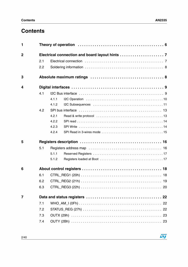
Contents
1 Theory of operation . . . . . . . . . . . . . . . . . . . . . . . . . . . . . . . . . . . . . . . . . 6
2 Electrical connection and board layout hints . . . . . . . . . . . . . . . . . . . . . 7
2.1 Electrical connection . . . . . . . . . . . . . . . . . . . . . . . . . . . . . . . . . . . . . . . . . 7
2.2 Soldering information . . . . . . . . . . . . . . . . . . . . . . . . . . . . . . . . . . . . . . . . . 8
3 Absolute maximum ratings . . . . . . . . . . . . . . . . . . . . . . . . . . . . . . . . . . . 8
4 Digital interfaces . . . . . . . . . . . . . . . . . . . . . . . . . . . . . . . . . . . . . . . . . . . . 9
4.1 I2C Bus interface . . . . . . . . . . . . . . . . . . . . . . . . . . . . . . . . . . . . . . . . . . . . 9
4.1.1 I2C Operation . . . . . . . . . . . . . . . . . . . . . . . . . . . . . . . . . . . . . . . . . . . . 10
4.1.2 I2C Subsequences . . . . . . . . . . . . . . . . . . . . . . . . . . . . . . . . . . . . . . . . 11
4.2 SPI bus interface . . . . . . . . . . . . . . . . . . . . . . . . . . . . . . . . . . . . . . . . . . . 13
4.2.1 Read & write protocol . . . . . . . . . . . . . . . . . . . . . . . . . . . . . . . . . . . . . . 13
4.2.2 SPI read . . . . . . . . . . . . . . . . . . . . . . . . . . . . . . . . . . . . . . . . . . . . . . . . . 14
4.2.3 SPI Write . . . . . . . . . . . . . . . . . . . . . . . . . . . . . . . . . . . . . . . . . . . . . . . . 14
4.2.4 SPI Read in 3-wires mode . . . . . . . . . . . . . . . . . . . . . . . . . . . . . . . . . . . 15
5 Registers description . . . . . . . . . . . . . . . . . . . . . . . . . . . . . . . . . . . . . . . 16
5.1 Registers address map . . . . . . . . . . . . . . . . . . . . . . . . . . . . . . . . . . . . . . 16
5.1.1 Reserved Registers . . . . . . . . . . . . . . . . . . . . . . . . . . . . . . . . . . . . . . . . 17
5.1.2 Registers loaded at Boot . . . . . . . . . . . . . . . . . . . . . . . . . . . . . . . . . . . . 17
6 About control registers . . . . . . . . . . . . . . . . . . . . . . . . . . . . . . . . . . . . . . 18
6.1 CTRL_REG1 (20h) . . . . . . . . . . . . . . . . . . . . . . . . . . . . . . . . . . . . . . . . . . 18
6.2 CTRL_REG2 (21h) . . . . . . . . . . . . . . . . . . . . . . . . . . . . . . . . . . . . . . . . . . 19
6.3 CTRL_REG3 (22h) . . . . . . . . . . . . . . . . . . . . . . . . . . . . . . . . . . . . . . . . . . 20
7 Data and status registers . . . . . . . . . . . . . . . . . . . . . . . . . . . . . . . . . . . . 22
7.1 WHO_AM_I (0Fh) . . . . . . . . . . . . . . . . . . . . . . . . . . . . . . . . . . . . . . . . . . . 22
7.2 STATUS_REG (27h) . . . . . . . . . . . . . . . . . . . . . . . . . . . . . . . . . . . . . . . . . 22
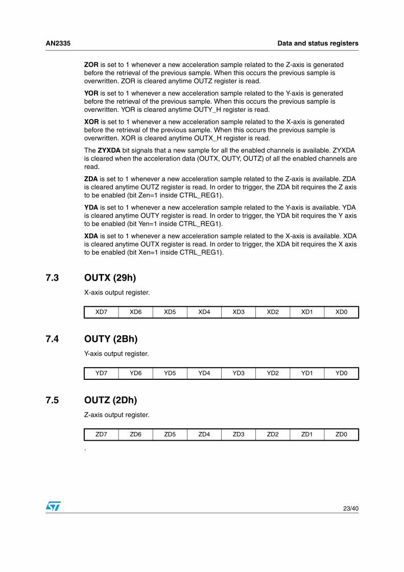
7.3 OUTX (29h) . . . . . . . . . . . . . . . . . . . . . . . . . . . . . . . . . . . . . . . . . . . . . . . 23
7.4 OUTY (2Bh) . . . . . . . . . . . . . . . . . . . . . . . . . . . . . . . . . . . . . . . . . . . . . . . 23

AN2335 Contents
3/40
7.5 OUTZ (2Dh) . . . . . . . . . . . . . . . . . . . . . . . . . . . . . . . . . . . . . . . . . . . . . . . 23
8 Free-Fall and Wake-Up Registers . . . . . . . . . . . . . . . . . . . . . . . . . . . . . 24
8.1 HP_FILTER_RESET (23h) . . . . . . . . . . . . . . . . . . . . . . . . . . . . . . . . . . . . 24
8.2 FF_WU_CFG_1 (30h) . . . . . . . . . . . . . . . . . . . . . . . . . . . . . . . . . . . . . . . 24
8.3 FF_WU_SRC_1 (31h) . . . . . . . . . . . . . . . . . . . . . . . . . . . . . . . . . . . . . . . 25
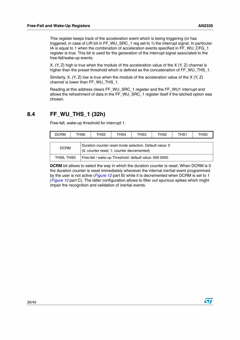
8.4 FF_WU_THS_1 (32h) . . . . . . . . . . . . . . . . . . . . . . . . . . . . . . . . . . . . . . . 26
8.5 FF_WU_DURATION_1 (33h) . . . . . . . . . . . . . . . . . . . . . . . . . . . . . . . . . . 27
8.6 FF_WU_CFG_2 (34h) . . . . . . . . . . . . . . . . . . . . . . . . . . . . . . . . . . . . . . . 28
8.7 FF_WU_SRC_2 (35h) . . . . . . . . . . . . . . . . . . . . . . . . . . . . . . . . . . . . . . . 29
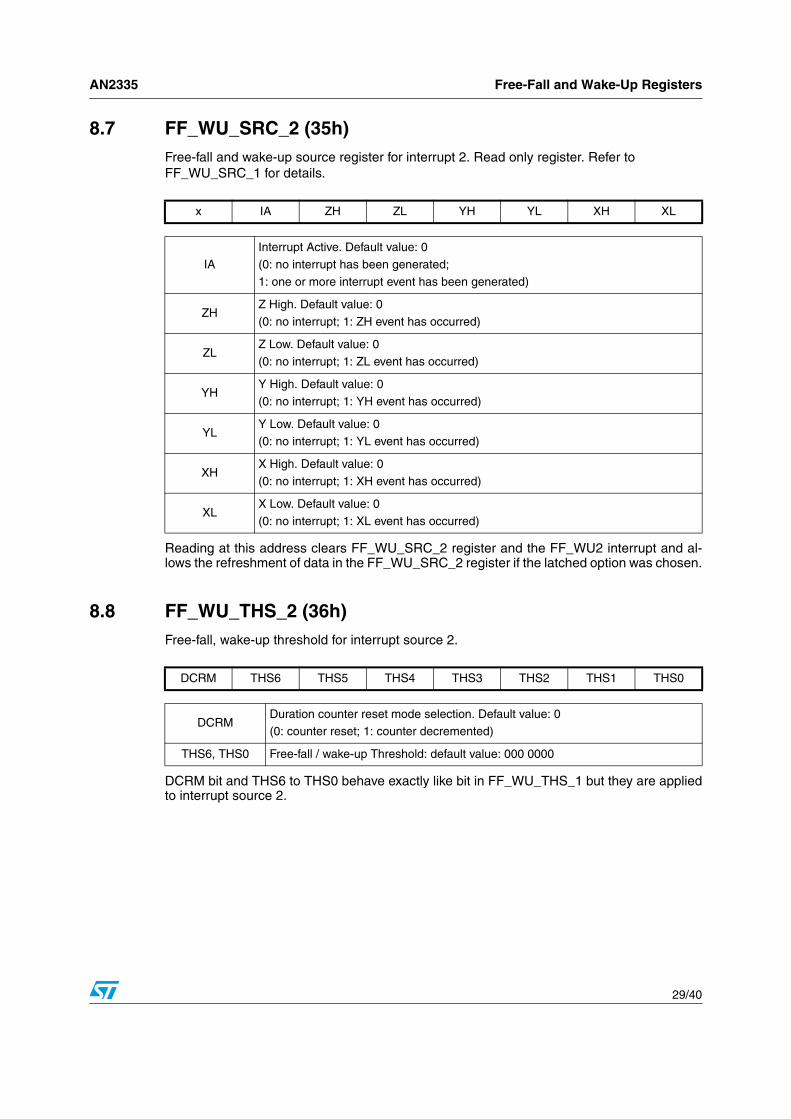
8.8 FF_WU_THS_2 (36h) . . . . . . . . . . . . . . . . . . . . . . . . . . . . . . . . . . . . . . . 29
8.9 FF_WU_DURATION_2 (37h) . . . . . . . . . . . . . . . . . . . . . . . . . . . . . . . . . . 30
9 Application Information . . . . . . . . . . . . . . . . . . . . . . . . . . . . . . . . . . . . . 31
9.1 START-UP SEQUENCE . . . . . . . . . . . . . . . . . . . . . . . . . . . . . . . . . . . . . . 31
9.2 READING ACCELERATION DATA . . . . . . . . . . . . . . . . . . . . . . . . . . . . . . 31
9.2.1 Using the Status Register . . . . . . . . . . . . . . . . . . . . . . . . . . . . . . . . . . . 31
9.2.2 Using the Data-Ready Signal . . . . . . . . . . . . . . . . . . . . . . . . . . . . . . . . 31
9.3 Understanding acceleration data . . . . . . . . . . . . . . . . . . . . . . . . . . . . . . . 32
9.4 Interrupt generation description . . . . . . . . . . . . . . . . . . . . . . . . . . . . . . . . 33
9.5 INERTIAL WAKE-UP . . . . . . . . . . . . . . . . . . . . . . . . . . . . . . . . . . . . . . . . 34
9.5.1 HP Filter Bypassed . . . . . . . . . . . . . . . . . . . . . . . . . . . . . . . . . . . . . . . . 34
9.5.2 Using the HP Filter . . . . . . . . . . . . . . . . . . . . . . . . . . . . . . . . . . . . . . . . . 35
9.6 Free-Fall Detection . . . . . . . . . . . . . . . . . . . . . . . . . . . . . . . . . . . . . . . . . . 36
9.6.1 Roll function not used . . . . . . . . . . . . . . . . . . . . . . . . . . . . . . . . . . . . . . 36
9.6.2 Roll function applied . . . . . . . . . . . . . . . . . . . . . . . . . . . . . . . . . . . . . . . 36
9.7 Output data rate selection and reading timing . . . . . . . . . . . . . . . . . . . . . 37
9.8 Data ready vs. interrupt signal . . . . . . . . . . . . . . . . . . . . . . . . . . . . . . . . . 38
10 Revision history . . . . . . . . . . . . . . . . . . . . . . . . . . . . . . . . . . . . . . . . . . . 39

List of tables AN2335
4/40
List of tables
Table 1. Absolute maximum ratings . . . . . . . . . . . . . . . . . . . . . . . . . . . . . . . . . . . . . . . . . . . . . . . . . . 8Table 2. Serial interface pin description . . . . . . . . . . . . . . . . . . . . . . . . . . . . . . . . . . . . . . . . . . . . . . . 9Table 3. Terminology . . . . . . . . . . . . . . . . . . . . . . . . . . . . . . . . . . . . . . . . . . . . . . . . . . . . . . . . . . . . . 9Table 4. Registers address map. . . . . . . . . . . . . . . . . . . . . . . . . . . . . . . . . . . . . . . . . . . . . . . . . . . . 16Table 5. Output Data Registers content vs. Acceleration . . . . . . . . . . . . . . . . . . . . . . . . . . . . . . . . . 32Table 6. Output Data Rate . . . . . . . . . . . . . . . . . . . . . . . . . . . . . . . . . . . . . . . . . . . . . . . . . . . . . . . . 37Table 7. Timing Value to Avoid Loosing the Data. . . . . . . . . . . . . . . . . . . . . . . . . . . . . . . . . . . . . . . 37Table 8. Document revision history . . . . . . . . . . . . . . . . . . . . . . . . . . . . . . . . . . . . . . . . . . . . . . . . . 39
AN2335 List of figures
5/40
List of figures
Figure 1. Device block diagram . . . . . . . . . . . . . . . . . . . . . . . . . . . . . . . . . . . . . . . . . . . . . . . . . . . . . . 6Figure 2. LIS302DL electrical connection . . . . . . . . . . . . . . . . . . . . . . . . . . . . . . . . . . . . . . . . . . . . . . 7Figure 3. I2C Subsequences . . . . . . . . . . . . . . . . . . . . . . . . . . . . . . . . . . . . . . . . . . . . . . . . . . . . . . . 12Figure 4. Read & write protocol . . . . . . . . . . . . . . . . . . . . . . . . . . . . . . . . . . . . . . . . . . . . . . . . . . . . . 13Figure 5. SPI read protocol . . . . . . . . . . . . . . . . . . . . . . . . . . . . . . . . . . . . . . . . . . . . . . . . . . . . . . . . 14Figure 6. Multiple bytes SPI read protocol (2 bytes example) . . . . . . . . . . . . . . . . . . . . . . . . . . . . . . 14Figure 7. SPI Write Protocol . . . . . . . . . . . . . . . . . . . . . . . . . . . . . . . . . . . . . . . . . . . . . . . . . . . . . . . 14Figure 8. Multiple Bytes SPI Write Protocol (2 bytes example) . . . . . . . . . . . . . . . . . . . . . . . . . . . . . 15Figure 9. SPI Read Protocol In 3-wires Mode . . . . . . . . . . . . . . . . . . . . . . . . . . . . . . . . . . . . . . . . . . 15Figure 10. Digital Processing Chain Block Diagram . . . . . . . . . . . . . . . . . . . . . . . . . . . . . . . . . . . . . . 20Figure 11. FF_WU_CFG_1,2 High and Low value . . . . . . . . . . . . . . . . . . . . . . . . . . . . . . . . . . . . . . . 25Figure 12. DCRM bit function. . . . . . . . . . . . . . . . . . . . . . . . . . . . . . . . . . . . . . . . . . . . . . . . . . . . . . . . 27Figure 13. Interrupt Generation Block Diagram . . . . . . . . . . . . . . . . . . . . . . . . . . . . . . . . . . . . . . . . . . 33Figure 14. Free-Fall, Wake-Up Interrupt Generator . . . . . . . . . . . . . . . . . . . . . . . . . . . . . . . . . . . . . . . 33Figure 15. Reading Timing. . . . . . . . . . . . . . . . . . . . . . . . . . . . . . . . . . . . . . . . . . . . . . . . . . . . . . . . . . 37Figure 16. Interrupt and dataready signal generation block diagram. . . . . . . . . . . . . . . . . . . . . . . . . . 38Figure 17. Data Ready Signal . . . . . . . . . . . . . . . . . . . . . . . . . . . . . . . . . . . . . . . . . . . . . . . . . . . . . . . 38
Theory of operation AN2335
6/40
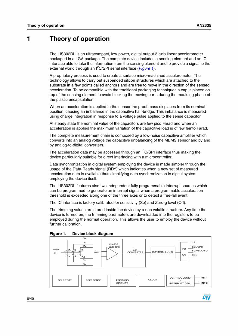
1 Theory of operation
The LIS302DL is an ultracompact, low-power, digital output 3-axis linear accelerometer packaged in a LGA package. The complete device includes a sensing element and an IC interface able to take the information from the sensing element and to provide a signal to the external world through an I2C/SPI serial interface (Figure 1).
A proprietary process is used to create a surface micro-machined accelerometer. The technology allows to carry out suspended silicon structures which are attached to the substrate in a few points called anchors and are free to move in the direction of the sensed acceleration. To be compatible with the traditional packaging techniques a cap is placed on top of the sensing element to avoid blocking the moving parts during the moulding phase of the plastic encapsulation.
When an acceleration is applied to the sensor the proof mass displaces from its nominal position, causing an imbalance in the capacitive half-bridge. This imbalance is measured using charge integration in response to a voltage pulse applied to the sense capacitor.
At steady state the nominal value of the capacitors are few pico Farad and when an acceleration is applied the maximum variation of the capacitive load is of few femto Farad.
The complete measurement chain is composed by a low-noise capacitive amplifier which converts into an analog voltage the capacitive unbalancing of the MEMS sensor and by and by analog-to-digital converters.
The acceleration data may be accessed through an I2C/SPI interface thus making the device particularly suitable for direct interfacing with a microcontroller.
Data synchronization in digital system employing the device is made simpler through the usage of the Data-Ready signal (RDY) which indicates when a new set of measured acceleration data is available thus simplifying data synchronization in digital system employing the device itself.
The LIS302DL features also two independent fully programmable interrupt sources which can be programmed to generate an interrupt signal when a programmable acceleration threshold is exceeded along one of the three axes or to detect a free-fall event.
The IC interface is factory calibrated for sensitivity (So) and Zero-g level (Off).
The trimming values are stored inside the device by a non volatile structure. Any time the device is turned on, the trimming parameters are downloaded into the registers to be employed during the normal operation. This allows the user to employ the device without further calibration.
Figure 1. Device block diagram
CHARGEAMPLIFIER
MUX
Y+
Z+
Y-
Z-
a
X+
X-
I2C
SPI
CS
SCL/SPC
SDA/SDO/SDI
SDO
CONTROL LOGIC&
INTERRUPT GEN.
INT 1 CLOCKTRIMMING
CIRCUITSREFERENCESELF TEST
CONTROL LOGICA/D
CONVERTER
INT 2
AN2335 Electrical connection and board layout hints
7/40
2 Electrical connection and board layout hints
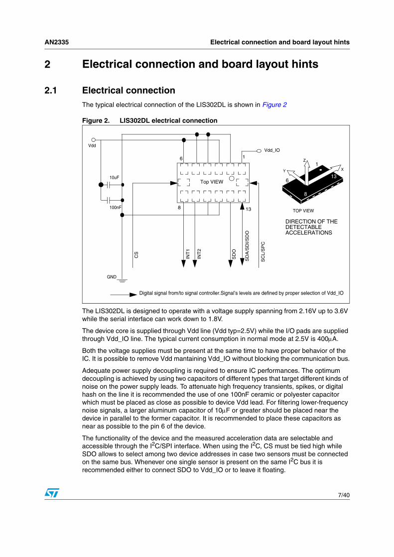
2.1 Electrical connectionThe typical electrical connection of the LIS302DL is shown in Figure 2
Figure 2. LIS302DL electrical connection
The LIS302DL is designed to operate with a voltage supply spanning from 2.16V up to 3.6V while the serial interface can work down to 1.8V.
The device core is supplied through Vdd line (Vdd typ=2.5V) while the I/O pads are supplied through Vdd_IO line. The typical current consumption in normal mode at 2.5V is 400μA.
Both the voltage supplies must be present at the same time to have proper behavior of the IC. It is possible to remove Vdd mantaining Vdd_IO without blocking the communication bus.
Adequate power supply decoupling is required to ensure IC performances. The optimum decoupling is achieved by using two capacitors of different types that target different kinds of noise on the power supply leads. To attenuate high frequency transients, spikes, or digital hash on the line it is recommended the use of one 100nF ceramic or polyester capacitor which must be placed as close as possible to device Vdd lead. For filtering lower-frequency noise signals, a larger aluminum capacitor of 10μF or greater should be placed near the device in parallel to the former capacitor. It is recommended to place these capacitors as near as possible to the pin 6 of the device.
The functionality of the device and the measured acceleration data are selectable and accessible through the I2C/SPI interface. When using the I2C, CS must be tied high while SDO allows to select among two device addresses in case two sensors must be connected on the same bus. Whenever one single sensor is present on the same I2C bus it is recommended either to connect SDO to Vdd_IO or to leave it floating.
6
8 13
1
Top VIEW
CS
10uF
Vdd
100nF
GND
Vdd_IO
SD
O
SD
A/S
DI/S
DO
INT
1
INT
2
SC
L/S
PC
Digital signal from/to signal controller.Signal’s levels are defined by proper selection of Vdd_IO
1
13
8
6
TOP VIEW
X
Z
Y
DIRECTION OF THEDETECTABLEACCELERATIONS
Absolute maximum ratings AN2335
8/40
2.2 Soldering information The LGA-14 package is lead free and green package qualified for soldering heat resistance according to JEDEC J-STD-020C. Land pattern and soldering recommendations are available upon request.
3 Absolute maximum ratings
Stresses above those listed as “absolute maximum ratings” may cause permanent damage to the device. This is a stress rating only and functional operation of the device under these conditions is not implied. Exposure to maximum rating conditions for extended periods may affect device reliability.
Warning: This is a ESD sensitive device, improper handling can cause permanent damages to the part.
Warning: This is a mechanical shock sensitive device, improper handling can cause permanent damages to the part.
Table 1. Absolute maximum ratings
Symbol Ratings Maximum Value Unit
Vdd Supply voltage(1)
1. Supply voltage on any pin should never exceed 6.0V
-0.3 to 6 V
Vdd_IO I/O pins Supply voltage(1) -0.3 to 6 V
VinInput voltage on any control pin
(CS, SCL/SPC, SDA/SDI/SDO, CK) -0.3 to Vdd_IO +0.3 V
APOW Acceleration (Any axis, Powered, Vdd=2.5V)3000g for 0.5 ms
10000g for 0.1 ms
AUNP Acceleration (Any axis, Unpowered)3000g for 0.5 ms
10000g for 0.1 ms
TOP Operating Temperature Range -40 to +85 °C
TSTG Storage Temperature Range -40 to +125 °C
ESD Electrostatic discharge protection Class 1: 0 - 2KV HBM
AN2335 Digital interfaces
9/40
4 Digital interfaces
The registers embedded inside the LIS302DL may be accessed through I2C and SPI serial interfaces. The latter may be SW configured to operate either in 3-wire or 4-wire interface mode.
The serial interfaces are mapped onto the same pads. To select/exploit the I2C interface, CS line must be tied high (i.e connected to Vdd_IO).
4.1 I2C Bus interfaceThe LIS302DL I2C is a bus slave. The I2C is employed to write/read the data into/from the registers.
The relevant I2C terminology is shown in Table 3:
There are two signals associated with the I2C bus: the Serial Clock Line (SCL) and the Serial DAta line (SDA). The latter is a bidirectional line used for sending and receiving the data to/from the interface. Both the lines are connected to Vdd_IO through a pull-up resistor embedded inside the LIS302DL. When the bus is free both the lines are high.
The I2C interface is compliant with Fast Mode (400 kHz) I2C standards as well as the Normal Mode.
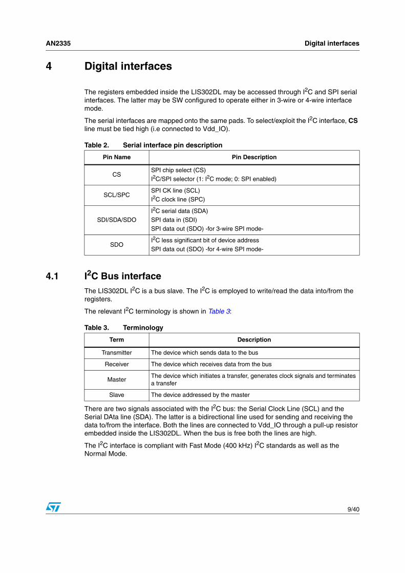
Table 2. Serial interface pin description
Pin Name Pin Description
CSSPI chip select (CS)
I2C/SPI selector (1: I2C mode; 0: SPI enabled)
SCL/SPCSPI CK line (SCL)
I2C clock line (SPC)
SDI/SDA/SDO
I2C serial data (SDA)
SPI data in (SDI)
SPI data out (SDO) -for 3-wire SPI mode-
SDOI2C less significant bit of device address
SPI data out (SDO) -for 4-wire SPI mode-
Table 3. Terminology
Term Description
Transmitter The device which sends data to the bus
Receiver The device which receives data from the bus
MasterThe device which initiates a transfer, generates clock signals and terminates a transfer
Slave The device addressed by the master

Digital interfaces AN2335
10/40
4.1.1 I2C Operation
The transaction on the bus is started through a START (ST) condition which is defined as a HIGH to LOW transition on the data line while the SCL line is held HIGH. After the START condition has been generated by the Master, the bus is considered busy. The next byte of data transmitted contains the address of the slave in the first 7 bits and the eighth bit tells whether the Master is receiving data from the slave or transmitting data to the slave (SAD subsequence). When an address is sent, each device in the system compares the first seven bits after a start condition with its own address. If they match, the device considers itself addressed by the Master.
The Slave ADdress (SAD) associated to the LIS302DL may be selected among the two predefined values 0011100b or 0011101b depending on the logic level present on SDO pin. In details, if SDO pin is either connected to Vdd_IO or left unconnected the slave address is 0011101b, otherwise when it is connected to GND the slave address is 0011100b. Whenever it is not needed to place two sensors on the same bus it is recommended to use the slave address 0011101b by either connecting the SDO pin to Vdd_IO or leaving it floating.
Data transfer with acknowledge is mandatory. The transmitter must release the SDA line during the acknowledge pulse. The receiver must then pull the data line LOW so that it remains stable low during the HIGH period of the acknowledge clock pulse. A receiver which has been addressed is obliged to generate an acknowledge after each byte of data has been received.
The I2C embedded inside the LIS302DL behaves like a slave device and the following protocol must be adhered to. After the start condition (ST) a salve address is sent, once a slave acknowledge (SAK) has been returned, a 8-bit sub-address will be transmitted: the 7 LSb represent the actual register address while the MSB enables address auto increment. If the MSb of the SUB field is 1, the SUB (register address) will be automatically incremented to allow multiple data read/write. Otherwise if the MSB of the SUB field is ‘0’, the SUB will remain unchanged and multiple read/write on the same address can be performed.
The slave address is completed with a Read/Write bit. If the bit was ‘1’ (Read), a repeated START (SR) condition will have to be issued after the two sub-address bytes; if the bit is ‘0’ (Write) the Master will transmit to the slave with direction unchanged.
Transfer when Master is writing one byte to slave
Transfer when Master is writing multiple bytes to slave:
Transfer when Master is receiving (reading) one byte of data from slave:
Master ST SAD + W SUB DATA SP
Slave SAK SAK SAK
Master ST SAD + W SUB DATA DATA SP
Slave SAK SAK SAK SAK
Master ST SAD + W SUB SR SAD + R NMAK SP
Slave SAK SAK SAK DATA
AN2335 Digital interfaces
11/40
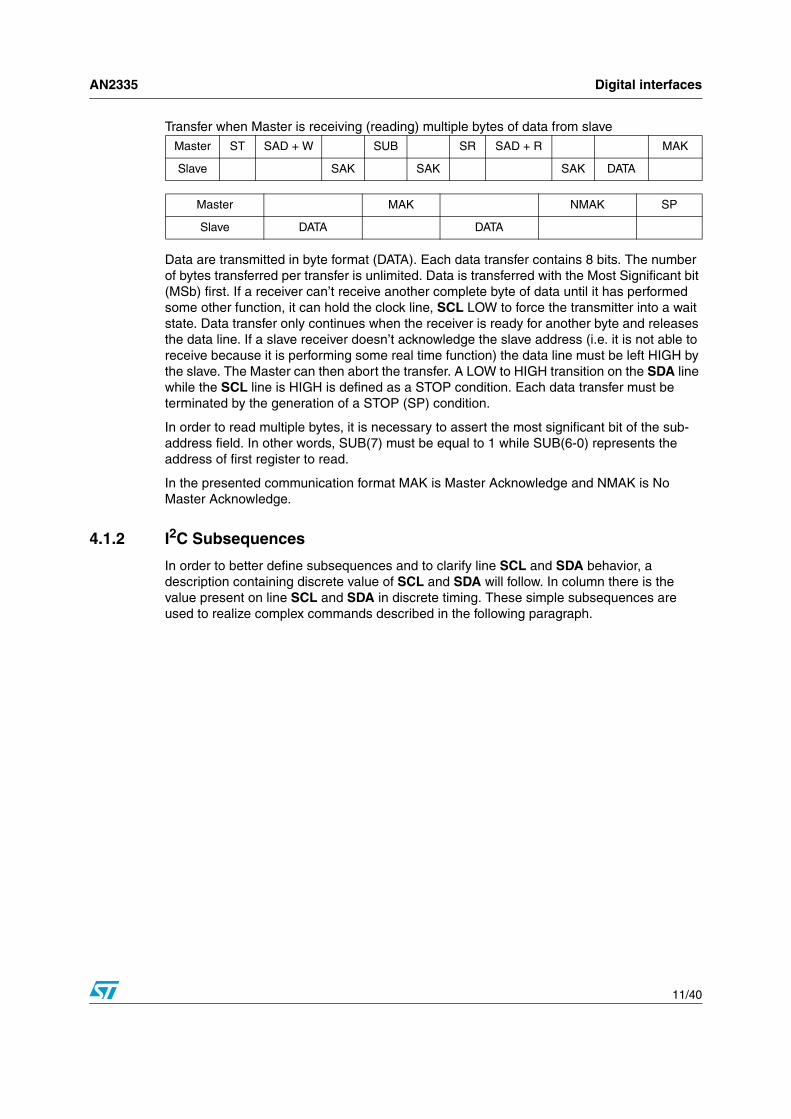
Transfer when Master is receiving (reading) multiple bytes of data from slave
Data are transmitted in byte format (DATA). Each data transfer contains 8 bits. The number of bytes transferred per transfer is unlimited. Data is transferred with the Most Significant bit (MSb) first. If a receiver can’t receive another complete byte of data until it has performed some other function, it can hold the clock line, SCL LOW to force the transmitter into a wait state. Data transfer only continues when the receiver is ready for another byte and releases the data line. If a slave receiver doesn’t acknowledge the slave address (i.e. it is not able to receive because it is performing some real time function) the data line must be left HIGH by the slave. The Master can then abort the transfer. A LOW to HIGH transition on the SDA line while the SCL line is HIGH is defined as a STOP condition. Each data transfer must be terminated by the generation of a STOP (SP) condition.
In order to read multiple bytes, it is necessary to assert the most significant bit of the sub-address field. In other words, SUB(7) must be equal to 1 while SUB(6-0) represents the address of first register to read.
In the presented communication format MAK is Master Acknowledge and NMAK is No Master Acknowledge.
4.1.2 I2C Subsequences
In order to better define subsequences and to clarify line SCL and SDA behavior, a description containing discrete value of SCL and SDA will follow. In column there is the value present on line SCL and SDA in discrete timing. These simple subsequences are used to realize complex commands described in the following paragraph.
Master ST SAD + W SUB SR SAD + R MAK
Slave SAK SAK SAK DATA
Master MAK NMAK SP
Slave DATA DATA
Digital interfaces AN2335
12/40
Figure 3. I2C Subsequences
ST: START condition
SCL 1111
SDA 1100
SR: Repeated START condition
SCL 1111
SDA 1100
SAD: Slave address (binary address: abcdefgh. In LIS302DL “abcdef” = “001110”)
SCL 00110 0110 0110 0110 0110 0110 0110 0110
SDA 0aaaa bbbb cccc dddd eeee f f f f gggg hhhh
Bit g=0 if SDO connected to GND, g=1 if SDO pad connected to VddBit h=0 => write, h=1 => read
SAK: Slave acknowledge (Z means high impedance)
SCL 0011
SDA (force) ZZZZ Check that SDA is 0 after SCL=1
SDA (read) XX00
SUB: Sub address (binary address: a0cdefgh)
SCL 00110 0110 0110 0110 0110 0110 0110 0110
SDA 0aaaa 0000 cccc dddd eeee f f f f gggg hhhh
Bit a=0 => do not increment address in multiple mode a=1 => increment address in multiple mode
DATA (Master): send DATA byte (binary number: abcdefgh)
SCL 00110 0110 0110 0110 0110 0110 0110 0110
SDA 0aaaa bbbb cccc dddd eeee f f f f gggg hhhh
DATA (Slave): read DATA byte (binary number: abcdefgh)
SCL 00110 0110 0110 0110 0110 0110 0110 0110
SDA (force) ZZZZ ZZZZ ZZZZ ZZZZ ZZZZ ZZZZ ZZZZ ZZZZ
SDA (read) a b c d e f g h
SP: STOP condition
SCL 1111
SDA 0011
MAK: Master Acknowledge
SCL 0011
SDA 0000
NMAK: No Master Acknowledge
SCL 0011
SDA ZZZZ or 1111
AN2335 Digital interfaces
13/40
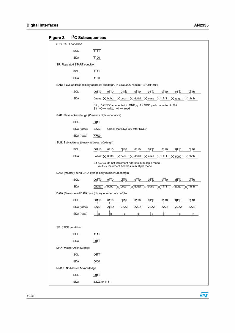
4.2 SPI bus interfaceThe LIS302DL SPI is a bus slave. The SPI allows to write and read the registers of the device.
The Serial Interface interacts with the outside world with 4 wires: CS, SPC, SPDI and SPDO.
4.2.1 Read & write protocol
Figure 4. Read & write protocol
CS is the Chip Select and it is controlled by the SPI master. It goes low at the start of the transmission and goes back high at the end. SPC is the Serial Port Clock and it is controlled by the SPI master. It is stopped high when CS is high (no transmission). SDI and SDO are respectively the Serial Port Data Input and Output. Those lines are driven at the falling edge of SPC and should be captured at the rising edge of SPC.
Both the Read Register and Write Register commands are completed in 16 clocks pulses or in multiple of 8 in case of multiple byte read/write. Bit duration is the time between two falling edges of SPC. The first bit (bit 0) starts at the first falling edge of SPC after the falling edge of CS while the last bit (bit 15, bit 23, ...) starts at the last falling edge of SPC just before the rising edge of CS.
bit 0: RW bit. When 0, the data DI(7:0) is written into the device. When 1, the data DO(7:0) from the device is read. In latter case, the chip will drive SDO at the start of bit 8.
bit 1: MS bit. When 0, the address will remain unchanged in multiple read/write commands. When 1, the address will be auto incremented in multiple read/write commands.
bit 2-7: address AD(5:0). This is the address field of the indexed register.
bit 8-15: data DI(7:0) (write mode). This is the data that will be written into the device (MSb first).
bit 8-15: data DO(7:0) (read mode). This is the data that will be read from the device (MSb first).
In multiple read/write commands further blocks of 8 clock periods will be added. When MS bit is 0 the address used to read/write data remains the same for every block. When MS bit is 1 the address used to read/write data is incremented at every block.
The function and the behavior of SDI and SDO remain unchanged.
CS
SPC
SDI
SDO
RWAD5 AD4 AD3 AD2 AD1 AD0
DI7 DI6 DI5 DI4 DI3 DI2 DI1 DI0
DO7 DO6 DO5 DO4 DO3 DO2 DO1 DO0
MS

Digital interfaces AN2335
14/40
4.2.2 SPI read
Figure 5. SPI read protocol
The SPI Read command is performed with 16 clocks pulses. Multiple byte read command is performed adding blocks of 8 clocks pulses at the previous one.
bit 0: READ bit. The value is 1.
bit 1: MS bit. When 0 do not increment address, when 1 increment address in multiple reading.
bit 2-7: address AD(5:0). This is the address field of the indexed register.
bit 8-15: data DO(7:0) (read mode). This is the data that will be read from the device (MSb first).
bit 16-... : data DO(...-8). Further data in multiple byte reading.
Figure 6. Multiple bytes SPI read protocol (2 bytes example)
4.2.3 SPI Write
Figure 7. SPI Write Protocol
CS
SPC
SDI
SDO
RW
DO7 DO6 DO5 DO4 DO3 DO2 DO1 DO0
AD5 AD4 AD3 AD2 AD1 AD0MS
CS
SPC
SDI
SDO
RW
DO7 DO6 DO5 DO4 DO3 DO2 DO1 DO0
AD5 AD4 AD3 AD2 AD1 AD0
DO15 DO14 DO13 DO12 DO11 DO10 DO9 DO8
MS
CS
SPC
SDI
RW DI7 DI6 DI5 DI4 DI3 DI2 DI1 DI0AD5 AD4 AD3 AD2 AD1 AD0MS

AN2335 Digital interfaces
15/40
The SPI Write command is performed with 16 clocks pulses. Multiple byte write command is performed adding blocks of 8 clocks pulses at the previous one.
bit 0: WRITE bit. The value is 0.
bit 1: MS bit. When 0 do not increment address, when 1 increment address in multiple writing.
bit 2 -7: address AD(5:0). This is the address field of the indexed register.
bit 8-15: data DI(7:0) (write mode). This is the data that will be written inside the device (MSb first).
bit 16-... : data DI(...-8). Further data in multiple byte writing.
Figure 8. Multiple Bytes SPI Write Protocol (2 bytes example)
4.2.4 SPI Read in 3-wires mode
3-wires mode is entered by setting to 1 bit SIM (SPI Serial Interface Mode selection) in CTRL_REG2.
Figure 9. SPI Read Protocol In 3-wires Mode
The SPI Read command is performed with 16 clocks pulses:
bit 0: READ bit. The value is 1.
bit 1: MS bit. When 0 do not increment address, when 1 increment address in multiple reading.
bit 2-7: address AD(5:0). This is the address field of the indexed register.
bit 8-15: data DO(7:0) (read mode). This is the data that will be read from the device (MSb first).
Multiple read command is also available in 3-wires mode.
CS
SPC
SDI
RWAD5 AD4 AD3 AD2 AD1 AD0
DI7 DI6 DI5 DI4 DI3 DI2 DI1 DI0 DI15 DI14 DI13 DI12 DI11 DI10 DI9 DI8
MS
CS
SPC
SDI
RW DO7 DO6 DO5 DO4 DO3 DO2 DO1 DO0AD5 AD4 AD3 AD2 AD1 AD0MS
Registers description AN2335
16/40
5 Registers description
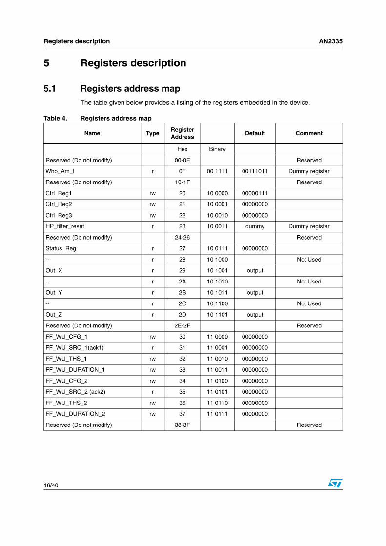
5.1 Registers address mapThe table given below provides a listing of the registers embedded in the device.
Table 4. Registers address map
Name TypeRegister Address
Default Comment
Hex Binary
Reserved (Do not modify) 00-0E Reserved
Who_Am_I r 0F 00 1111 00111011 Dummy register
Reserved (Do not modify) 10-1F Reserved
Ctrl_Reg1 rw 20 10 0000 00000111
Ctrl_Reg2 rw 21 10 0001 00000000
Ctrl_Reg3 rw 22 10 0010 00000000
HP_filter_reset r 23 10 0011 dummy Dummy register
Reserved (Do not modify) 24-26 Reserved
Status_Reg r 27 10 0111 00000000
-- r 28 10 1000 Not Used
Out_X r 29 10 1001 output
-- r 2A 10 1010 Not Used
Out_Y r 2B 10 1011 output
-- r 2C 10 1100 Not Used
Out_Z r 2D 10 1101 output
Reserved (Do not modify) 2E-2F Reserved
FF_WU_CFG_1 rw 30 11 0000 00000000
FF_WU_SRC_1(ack1) r 31 11 0001 00000000
FF_WU_THS_1 rw 32 11 0010 00000000
FF_WU_DURATION_1 rw 33 11 0011 00000000
FF_WU_CFG_2 rw 34 11 0100 00000000
FF_WU_SRC_2 (ack2) r 35 11 0101 00000000
FF_WU_THS_2 rw 36 11 0110 00000000
FF_WU_DURATION_2 rw 37 11 0111 00000000
Reserved (Do not modify) 38-3F Reserved

AN2335 Registers description
17/40
5.1.1 Reserved Registers
Registers marked as reserved must not be changed. Random changes of the content of those registers might cause permanent damages to the device.
5.1.2 Registers loaded at Boot
The LIS302DL is factory trimmed. The content of the registers that are loaded at boot must not be changed. Their content is automatically restored when the device is powered-up.
About control registers AN2335
18/40
6 About control registers
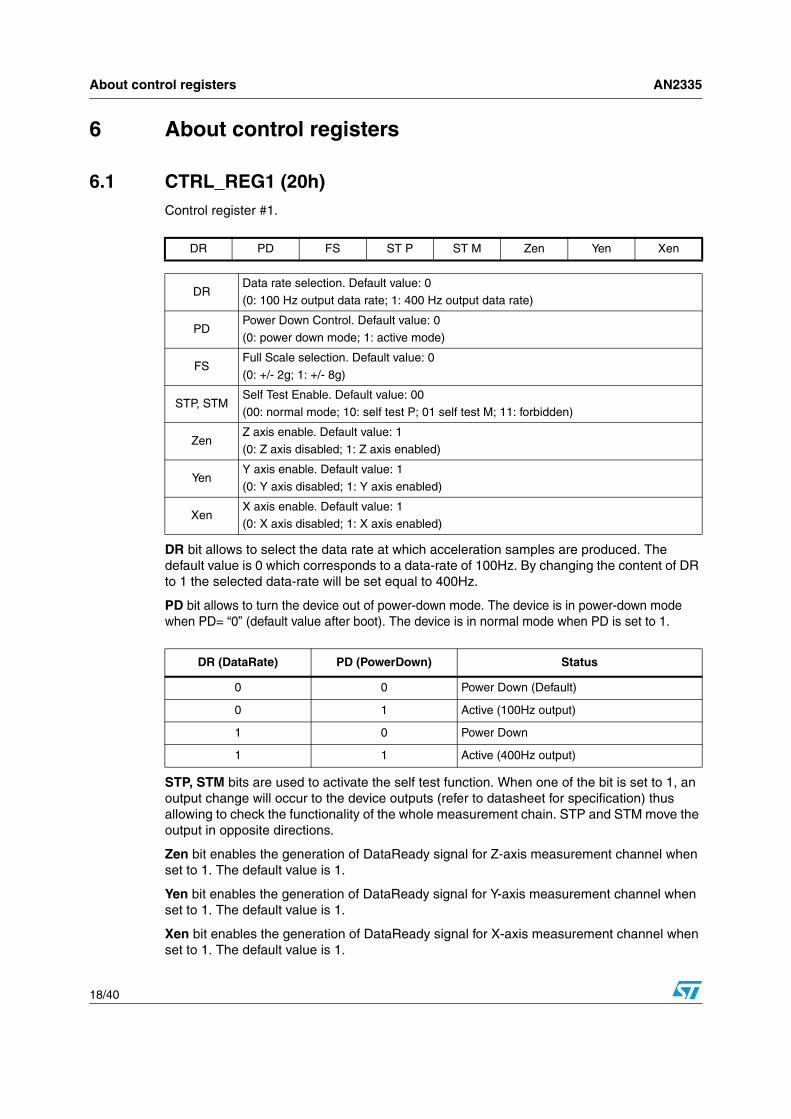
6.1 CTRL_REG1 (20h)Control register #1.
DR bit allows to select the data rate at which acceleration samples are produced. The default value is 0 which corresponds to a data-rate of 100Hz. By changing the content of DR to 1 the selected data-rate will be set equal to 400Hz.
PD bit allows to turn the device out of power-down mode. The device is in power-down mode when PD= “0” (default value after boot). The device is in normal mode when PD is set to 1.
STP, STM bits are used to activate the self test function. When one of the bit is set to 1, an output change will occur to the device outputs (refer to datasheet for specification) thus allowing to check the functionality of the whole measurement chain. STP and STM move the output in opposite directions.
Zen bit enables the generation of DataReady signal for Z-axis measurement channel when set to 1. The default value is 1.
Yen bit enables the generation of DataReady signal for Y-axis measurement channel when set to 1. The default value is 1.
Xen bit enables the generation of DataReady signal for X-axis measurement channel when set to 1. The default value is 1.
DR PD FS ST P ST M Zen Yen Xen
DRData rate selection. Default value: 0
(0: 100 Hz output data rate; 1: 400 Hz output data rate)
PDPower Down Control. Default value: 0
(0: power down mode; 1: active mode)
FSFull Scale selection. Default value: 0(0: +/- 2g; 1: +/- 8g)
STP, STMSelf Test Enable. Default value: 00
(00: normal mode; 10: self test P; 01 self test M; 11: forbidden)
ZenZ axis enable. Default value: 1
(0: Z axis disabled; 1: Z axis enabled)
YenY axis enable. Default value: 1
(0: Y axis disabled; 1: Y axis enabled)
XenX axis enable. Default value: 1(0: X axis disabled; 1: X axis enabled)
DR (DataRate) PD (PowerDown) Status
0 0 Power Down (Default)
0 1 Active (100Hz output)
1 0 Power Down
1 1 Active (400Hz output)

AN2335 About control registers
19/40
6.2 CTRL_REG2 (21h)Control register #2.
SIM bit selects the SPI Serial Interface Mode. When SIM is ‘0’ (default value) the 4-wire interface mode is selected. The data coming from the device are sent to SDO pad. In 3-wire interface mode output data are sent to SDA/SDI pad.
BOOT bit is used to refresh the content of internal registers stored in the flash memory block. At the device power up the content of the flash memory block is transferred to the internal registers related to trimming functions to permit a good behavior of the device itself. If for any reason the content of trimming registers was changed it is sufficient to use this bit to restore correct values. When BOOT bit is set to ‘1’ the content of internal flash is copied inside corresponding internal registers and it is used to calibrate the device. These values are factory trimmed, they are different for every accelerometer and normally they have not to be changed. At the end of the boot process the BOOT bit is set again to ‘0’.
FDS bit enables (FDS=1) or bypass (FDS=0) the high pass filter in the signal chain of the sensor.
HP FF_WU[2:1]. These bits enable (HP FF_WU=1) or bypass (HP FF_WU=0) the high pass filter in interrupt generation blocks.
HP coeff[2:1]. These bits are used to configure high-pass filter cut-off frequency ft accordingly to the table given below:
SIM BOOT -- FDSHP
FF_WU2HP
FF_WU1HP coeff2 HP coeff1
SIMSPI Serial Interface Mode selection. Default value: 0(0: 4-wire interface; 1: 3-wire interface)
BOOTReboot memory content. Default value: 0(0: normal mode; 1: reboot memory content)
FDSFiltered Data Selection. Default value: 0(0: internal filter bypassed; 1: data from internal filter sent to output register)
HP FF_WU2High Pass filter enabled for FreeFall/WakeUp # 2. Default value: 0(0: filter bypassed; 1: filter enabled)
HP FF_WU1High Pass filter enabled for Free-Fall/Wake-Up #1. Default value: 0
(0: filter bypassed; 1: filter enabled)
HP coeff2
HP coeff1
High pass filter cut-off frequency configuration. Default value: 00
HPcoeff2,1ft (Hz)
(DR=100 Hz)ft (Hz)
(DR=400 Hz)
00 2 8
01 1 4
10 0.5 2
11 0.25 1

About control registers AN2335
20/40
Figure 10 shows the block diagram of the digital processing chain and the related control signals.
Figure 10. Digital Processing Chain Block Diagram
6.3 CTRL_REG3 (22h)Control register #3.
IHL bit selects the polarity of the interrupt signal. When IHL is ‘0’ (default value) any interrupt event will signalled with a logical 1.
PP_OD bit defines whether the interrupt pad has to work in Push-pull or in Open Drain mode. The latter is specifically intended for wired-or connection of multiple interrupt signals on the same interrupt line. The default value is ‘0’ which corresponds to push-pull mode.
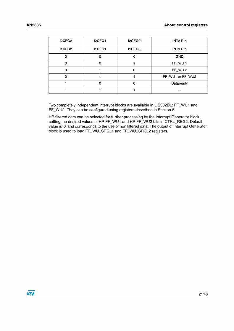
I2CFG[2:0] and I1CFG[2:0] bit select which signal has to be sent out from the INT2 and INT1 interrupt pads as described in the following table:
HP Filter
Interrupt Generator(FF_WU 1)
CTRL_REG2(HP FF_WU1)
0
CTRL_REG3(FDS)
0
Regs Array
Digital Processing Chain
HP_FILTER_RESET
1
1
Interrupt Generator(FF_WU 2)
CTRL_REG2(HP FF_WU2)
0
1
Offset
Output regs
SRC reg 1
SRC reg 2
AdjustmentBlock
IHL PP_OD I2CFG2 I2CFG1 I2CFG0 I1CFG2 I1CFG1 I1CFG0
IHLInterrupt active high, low. Default value 0.(0: active high; 1: active low)
PP_ODPush-pull/Open Drain selection on interrupt pad. Default value 0.(0: push-pull; 1: open drain)
I2CFG2,
I2CFG0
Interrupt 2 configuration bits. Default value 000.
(see table below)
I1CFG2, I1CFG0
Interrupt 1 configuration bits. Default value 000.
(see table below)
AN2335 About control registers
21/40
Two completely independent interrupt blocks are available in LIS302DL: FF_WU1 and FF_WU2. They can be configured using registers described in Section 8.
HP filtered data can be selected for further processing by the Interrupt Generator block setting the desired values of HP FF_WU1 and HP FF_WU2 bits in CTRL_REG2. Default value is '0' and corresponds to the use of non filtered data. The output of Interrupt Generator block is used to load FF_WU_SRC_1 and FF_WU_SRC_2 registers.
I2CFG2 I2CFG1 I2CFG0 INT2 Pin
I1CFG2 I1CFG1 I1CFG0 INT1 Pin
0 0 0 GND
0 0 1 FF_WU 1
0 1 0 FF_WU 2
0 1 1 FF_WU1 or FF_WU2
1 0 0 Dataready
1 1 1 --
Data and status registers AN2335
22/40
7 Data and status registers
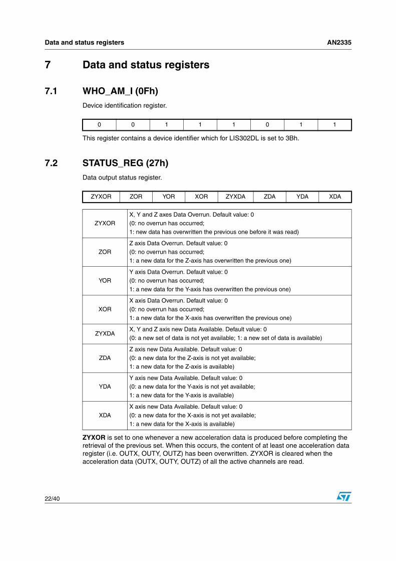
7.1 WHO_AM_I (0Fh)Device identification register.
This register contains a device identifier which for LIS302DL is set to 3Bh.
7.2 STATUS_REG (27h)Data output status register.
ZYXOR is set to one whenever a new acceleration data is produced before completing the retrieval of the previous set. When this occurs, the content of at least one acceleration data register (i.e. OUTX, OUTY, OUTZ) has been overwritten. ZYXOR is cleared when the acceleration data (OUTX, OUTY, OUTZ) of all the active channels are read.
0 0 1 1 1 0 1 1
ZYXOR ZOR YOR XOR ZYXDA ZDA YDA XDA
ZYXOR
X, Y and Z axes Data Overrun. Default value: 0
(0: no overrun has occurred;
1: new data has overwritten the previous one before it was read)
ZOR
Z axis Data Overrun. Default value: 0
(0: no overrun has occurred; 1: a new data for the Z-axis has overwritten the previous one)
YORY axis Data Overrun. Default value: 0(0: no overrun has occurred;
1: a new data for the Y-axis has overwritten the previous one)
XOR
X axis Data Overrun. Default value: 0
(0: no overrun has occurred;
1: a new data for the X-axis has overwritten the previous one)
ZYXDAX, Y and Z axis new Data Available. Default value: 0
(0: a new set of data is not yet available; 1: a new set of data is available)
ZDA
Z axis new Data Available. Default value: 0
(0: a new data for the Z-axis is not yet available; 1: a new data for the Z-axis is available)
YDAY axis new Data Available. Default value: 0(0: a new data for the Y-axis is not yet available;
1: a new data for the Y-axis is available)
XDA
X axis new Data Available. Default value: 0
(0: a new data for the X-axis is not yet available;
1: a new data for the X-axis is available)
AN2335 Data and status registers
23/40
ZOR is set to 1 whenever a new acceleration sample related to the Z-axis is generated before the retrieval of the previous sample. When this occurs the previous sample is overwritten. ZOR is cleared anytime OUTZ register is read.
YOR is set to 1 whenever a new acceleration sample related to the Y-axis is generated before the retrieval of the previous sample. When this occurs the previous sample is overwritten. YOR is cleared anytime OUTY_H register is read.
XOR is set to 1 whenever a new acceleration sample related to the X-axis is generated before the retrieval of the previous sample. When this occurs the previous sample is overwritten. XOR is cleared anytime OUTX_H register is read.
The ZYXDA bit signals that a new sample for all the enabled channels is available. ZYXDA is cleared when the acceleration data (OUTX, OUTY, OUTZ) of all the enabled channels are read.
ZDA is set to 1 whenever a new acceleration sample related to the Z-axis is available. ZDA is cleared anytime OUTZ register is read. In order to trigger, the ZDA bit requires the Z axis to be enabled (bit Zen=1 inside CTRL_REG1).
YDA is set to 1 whenever a new acceleration sample related to the Y-axis is available. YDA is cleared anytime OUTY register is read. In order to trigger, the YDA bit requires the Y axis to be enabled (bit Yen=1 inside CTRL_REG1).
XDA is set to 1 whenever a new acceleration sample related to the X-axis is available. XDA is cleared anytime OUTX register is read. In order to trigger, the XDA bit requires the X axis to be enabled (bit Xen=1 inside CTRL_REG1).
7.3 OUTX (29h)X-axis output register.
7.4 OUTY (2Bh)Y-axis output register.
.
7.5 OUTZ (2Dh)Z-axis output register.
.
XD7 XD6 XD5 XD4 XD3 XD2 XD1 XD0
YD7 YD6 YD5 YD4 YD3 YD2 YD1 YD0
ZD7 ZD6 ZD5 ZD4 ZD3 ZD2 ZD1 ZD0

Free-Fall and Wake-Up Registers AN2335
24/40
8 Free-Fall and Wake-Up Registers
The following sections describes the registers that are involved in the generation of the interrupt signal associated to the inertial wake-up and free-fall events.
8.1 HP_FILTER_RESET (23h)Dummy register. A reading at this address forces the high-pass filter to recover instantaneously the dc level of the acceleration signal provided to its inputs. After the above reading the output of the high-pass filter will be zero.
8.2 FF_WU_CFG_1 (30h)Free-fall and wake-up configuration register for interrupt source 1.
.
X X X X X X X X
AOI LIR ZHIE ZLIE YHIE YLIE XHIE XLIE
AOIAnd/Or combination of Interrupt events. Default value: 0
(0: OR combination of interrupt events; 1: AND combination of interrupt events)
LIRLatch Interrupt request into FF_WU_SRC reg with the FF_WU_SRC reg cleared by reading FF_WU_SRC_1 reg. Default value: 0(0: interrupt request not latched; 1: interrupt request latched)
ZHIEEnable interrupt generation on Z high event. Default value: 0(0: disable interrupt request;
1: enable interrupt request on measured accel. value higher than preset threshold)
ZLIE
Enable interrupt generation on Z low event. Default value: 0
(0: disable interrupt request;
1: enable interrupt request on measured accel. value lower than preset threshold)
YHIE
Enable interrupt generation on Y high event. Default value: 0
(0: disable interrupt request;1: enable interrupt request on measured accel. value higher than preset threshold)
YLIEEnable interrupt generation on Y low event. Default value: 0(0: disable interrupt request;
1: enable interrupt request on measured accel. value lower than preset threshold)
XHIE
Enable interrupt generation on X high event. Default value: 0
(0: disable interrupt request;
1: enable interrupt request on measured accel. value higher than preset threshold)
XLIE
Enable interrupt generation on X low event. Default value: 0
(0: disable interrupt request;1: enable interrupt request on measured accel. value lower than preset threshold)

AN2335 Free-Fall and Wake-Up Registers
25/40
AOI bit allows to select between Wake-Up (OR combination of interrupt events) and Free-Fall (AND combination of interrupt events) detection
LIR defines whether the configured interrupt event has to be latched by the device once it has happened. The interrupt request is cleared by reading the related source reg (FF_WU_SRC_1).
XHIE (YHIE, ZHIE) set an interrupt event to occur when the measured acceleration data on X (Y, Z) channel is higher than the threshold set in FF_WU_THS_1 register.
XLIE (YLIE, ZLIE) set an interrupt event to occur when the measured acceleration data on X (Y, Z) channel is lower than the threshold set in FF_WU_THS_1 register.
The threshold module which is used by the system to detect any free-fall or inertial wake-up event is defined by FF_WU_THS_1. The threshold value is expressed over 7 bit as an unsigned number and X, (Y, Z) high is true when the unsigned acceleration value of the X (Y, Z) channel is higher than or egual to FF_WU_THS_1. Similarly, X, (Y, Z) low is true when the unsigned acceleration value of the X (Y, Z) channel is lower than FF_WU_THS_1. Refer to Figure 11 for more details.
Figure 11. FF_WU_CFG_1,2 High and Low value
8.3 FF_WU_SRC_1 (31h)Free-fall and wake-up source register for interrupt 1. Read only register.
.
+ Full Scale
- Full Scale
0 g level
Threshold module
Threshold module
X (Y, Z) high
X (Y, Z) high
X (Y, Z) low
Positive
Negative
acceleration
acceleration
x IA ZH ZL YH YL XH XL
IA
Interrupt Active. Default value: 0
(0: no interrupt has been generated; 1: one or more interrupt event has been generated)
ZHZ High. Default value: 0
(0: no interrupt; 1: ZH event has occurred)
ZLZ Low. Default value: 0
(0: no interrupt; 1: ZL event has occurred)
YHY High. Default value: 0(0: no interrupt; 1: YH event has occurred)
YLY Low. Default value: 0
(0: no interrupt; 1: YL event has occurred)
XHX High. Default value: 0
(0: no interrupt; 1: XH event has occurred)
XLX Low. Default value: 0(0: no interrupt; 1: XL event has occurred)
Free-Fall and Wake-Up Registers AN2335
26/40
This register keeps track of the acceleration event which is being triggering (or has triggered, in case of LIR bit in FF_WU_SRC_1 reg set to 1) the interrupt signal. In particular IA is equal to 1 when the combination of acceleration events specified in FF_WU_CFG_1 register is true. This bit is used for the generation of the interrupt signal associated to the free-fall/wake-up events.
X, (Y, Z) high is true when the module of the acceleration value of the X (Y, Z) channel is higher than the preset threshold which is defined as the concatenation of FF_WU_THS_1.
Similarly, X, (Y, Z) low is true when the module of the acceleration value of the X (Y, Z) channel is lower than FF_WU_THS_1.
Reading at this address clears FF_WU_SRC_1 register and the FF_WU1 interrupt and allows the refreshment of data in the FF_WU_SRC_1 register itself if the latched option was chosen.
8.4 FF_WU_THS_1 (32h)Free-fall, wake-up threshold for interrupt 1.
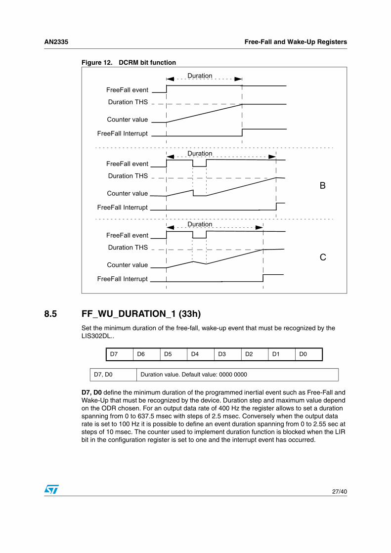
DCRM bit allows to select the way in which the duration counter is reset. When DCRM is 0 the duration counter is reset immediately whenever the internal inertial event programmed by the user is not active (Figure 12 part B) while it is decremented when DCRM is set to 1 (Figure 12 part C). The latter configuration allows to filter out spurious spikes which might impair the recognition and validation of inertial events.
DCRM THS6 THS5 THS4 THS3 THS2 THS1 THS0
DCRMDuration counter reset mode selection. Default value: 0(0: counter reset; 1: counter decremented)
THS6, THS0 Free-fall / wake-up Threshold: default value: 000 0000
AN2335 Free-Fall and Wake-Up Registers
27/40
Figure 12. DCRM bit function
8.5 FF_WU_DURATION_1 (33h)Set the minimum duration of the free-fall, wake-up event that must be recognized by the LIS302DL..
D7, D0 define the minimum duration of the programmed inertial event such as Free-Fall and Wake-Up that must be recognized by the device. Duration step and maximum value depend on the ODR chosen. For an output data rate of 400 Hz the register allows to set a duration spanning from 0 to 637.5 msec with steps of 2.5 msec. Conversely when the output data rate is set to 100 Hz it is possible to define an event duration spanning from 0 to 2.55 sec at steps of 10 msec. The counter used to implement duration function is blocked when the LIR bit in the configuration register is set to one and the interrupt event has occurred.
FreeFall event
Counter value
Duration THS
FreeFall Interrupt
FreeFall event
Counter value
Duration THS
FreeFall Interrupt
FreeFall event
Counter value
Duration THS
FreeFall Interrupt
Duration
Duration
Duration
C
B
D7 D6 D5 D4 D3 D2 D1 D0
D7, D0 Duration value. Default value: 0000 0000

Free-Fall and Wake-Up Registers AN2335
28/40
8.6 FF_WU_CFG_2 (34h)Free-fall and wake-up configuration register for interrupt source 2.
Two structures can be used to generate interrupts. They have exactly the same configuration capability and they are completely independent.The interrupt result of each structure can be sent indifferently to INT1 or INT2 pin usingCTRL_Reg3 register.
AOI LIR ZHIE ZLIE YHIE YLIE XHIE XLIE
AOIAnd/Or combination of Interrupt events. Default value: 0
(0: OR combination of interrupt events; 1: AND combination of interrupt events)
LIRLatch Interrupt request into FF_WU_SRC reg with the FF_WU_SRC reg cleared by reading FF_WU_SRC_1 reg. Default value: 0(0: interrupt request not latched; 1: interrupt request latched)
ZHIEEnable interrupt generation on Z high event. Default value: 0(0: disable interrupt request;
1: enable interrupt request on measured accel. value higher than preset threshold)
ZLIE
Enable interrupt generation on Z low event. Default value: 0
(0: disable interrupt request;
1: enable interrupt request on measured accel. value lower than preset threshold)
YHIE
Enable interrupt generation on Y high event. Default value: 0
(0: disable interrupt request;
1: enable interrupt request on measured accel. value higher than preset threshold)
YLIE
Enable interrupt generation on Y low event. Default value: 0
(0: disable interrupt request;1: enable interrupt request on measured accel. value lower than preset threshold)
XHIEEnable interrupt generation on X high event. Default value: 0 (0: disable interrupt request;
1: enable interrupt request on measured accel. value higher than preset threshold)
XLIE
Enable interrupt generation on X low event. Default value: 0
(0: disable interrupt request;
1: enable interrupt request on measured accel. value lower than preset threshold)
AN2335 Free-Fall and Wake-Up Registers
29/40
8.7 FF_WU_SRC_2 (35h)Free-fall and wake-up source register for interrupt 2. Read only register. Refer to FF_WU_SRC_1 for details.
Reading at this address clears FF_WU_SRC_2 register and the FF_WU2 interrupt and al-lows the refreshment of data in the FF_WU_SRC_2 register if the latched option was chosen.
8.8 FF_WU_THS_2 (36h)Free-fall, wake-up threshold for interrupt source 2.
DCRM bit and THS6 to THS0 behave exactly like bit in FF_WU_THS_1 but they are appliedto interrupt source 2.
x IA ZH ZL YH YL XH XL
IA
Interrupt Active. Default value: 0
(0: no interrupt has been generated;
1: one or more interrupt event has been generated)
ZHZ High. Default value: 0
(0: no interrupt; 1: ZH event has occurred)
ZLZ Low. Default value: 0
(0: no interrupt; 1: ZL event has occurred)
YHY High. Default value: 0
(0: no interrupt; 1: YH event has occurred)
YLY Low. Default value: 0
(0: no interrupt; 1: YL event has occurred)
XHX High. Default value: 0
(0: no interrupt; 1: XH event has occurred)
XLX Low. Default value: 0
(0: no interrupt; 1: XL event has occurred)
DCRM THS6 THS5 THS4 THS3 THS2 THS1 THS0
DCRMDuration counter reset mode selection. Default value: 0(0: counter reset; 1: counter decremented)
THS6, THS0 Free-fall / wake-up Threshold: default value: 000 0000

Free-Fall and Wake-Up Registers AN2335
30/40
8.9 FF_WU_DURATION_2 (37h)Set the minimum duration of the free-fall, wake-up event that must be recognized by the LIS302DL.
Refer to FF_WU_DURATION_1 for details.
D7 D6 D5 D4 D3 D2 D1 D0
D7, D0 Duration value. Default value: 0000 0000
AN2335 Application Information
31/40
9 Application Information
9.1 START-UP SEQUENCEOnce the device is powered-up it automatically downloads the calibration coefficients from the embedded flash to the internal registers. When the boot procedure is completed, i.e. approximately after 3 milli-seconds, the device automatically enters power-down mode.
To turn-on the device and gather acceleration data it is necessary to write 47h inside the CTRL_REG1. With this command the three acceleration channels (i.e. X, Y and Z axis) are enabled and the Output Data Rate is set to 100 Hz.
9.2 READING ACCELERATION DATA
9.2.1 Using the Status Register
The device is provided with a STATUS_REG which should be polled to check when a new set of data is available. The reading procedure should be the following:
The check performed at step 3 allows to understand whether the reading rate is adequate compared to the data production rate. In case one or more acceleration samples have been overwritten by new data because of a reading rate too slow, the bit STATUS_REG(7) will be set to 1.
The overrun bit are automatically cleared when all the data present inside the device have been read and new data have not been produced in the meanwhile.
9.2.2 Using the Data-Ready Signal
The device may be configured to generate one HW signal (Data Ready) on either pin 8 or 9 to flag that a new set of measurement data is available for reading. This signal corresponds to the ZYXDA bit present inside the STATUS_REG. The polarity of the signal is defined through the IHL bit present inside the CTRL_REG3 and it is deasserted when the acceleration data of all the enabled channels have been read. To enable Data Ready signal on pin #8 (corresponding to INT1) it is necessary to set I1CFG[2:0] bit present inside the CTRL_REG3 to 100. Conversely, to enable Data Ready signal on pin #9 (corresponding to INT2) it is necessary to set I2CFG[2:0] bit present inside the CTRL_REG3 to 100.
1 read STATUS_REG
2 if STATUS_REG(3)=0 then goto 1
3 if STATUS_REG(7)=1 then some data have been overwritten
4 read OUTX
5 read OUTY
6 read OUTZ
7 data processing
8 goto 1
Application Information AN2335
32/40
9.3 Understanding acceleration dataThe measured acceleration data are sent into OUTX, OUTY and OUTZ registers. The acceleration values are expressed as a 2’s complement number. When the full-scale is set to 2g, each LSB corresponds to 18mg.
The table below provides few basic examples of the data that will be read in the data registers when the device is subject to a given acceleration. The values listed in the table are given under the hypothesis of perfect device calibration (i.e no offset, no gain error, ....) and rounded to the closest integer.
Table 5. Output Data Registers content vs. Acceleration
Acceleration ValuesFS bit = 0 FS bit = 1
Output Register Content
0g 00h 00h
350mg 14h 05h
1g 38h 0Eh
2g 6Fh 1Ch
-350mg ECh FBh
-1g C8h F2h
-2g 91h E4h
AN2335 Application Information
33/40
9.4 Interrupt generation descriptionThe LIS302DL provide two fully-programmable interrupt sources which may be configured to trigger different inertial events. Among them it is worth mentioning the recognition of Free-Fall and Wake-Up events. Whenever an interrupt condition is verified the interrupt signal is asserted and reading either the FF_WU_SRC_1 or FF_WU_SRC_2 registers it is possible to understand which condition has occurred.
The block diagram of the interrupt block is given in the pictures below.
Figure 13. Interrupt Generation Block Diagram
Figure 14. Free-Fall, Wake-Up Interrupt Generator
FF or WU interrupt generation is selected for each interrupt generation channel through AOI bit in the corresponding FF_WU_CFG register. If AOI bit is ‘0’ signals coming from comparators are put in logical or. Depending on values written in FF_WU_CFG_1 and FF_WU_CFG_2 registers every time the value of at least one of the enabled axes exceeds the threshold written in module in the corresponding FF_WU_THS_1 and FF_WU_THS_2 registers a FF, WU interrupt is generated. Otherwise if AOI bit is ‘1’ signals coming from comparators are going into a “NAND” port. In this case an interrupt signal is generated whenever the acceleration signal of all the enabled axes is below the threshold written in FF_WU_THS_1 or FF_WU_THS_2 registers.
Ph_Gen
Ctrl_reg1(DR,PD)
100/400Hz
ADC 0
1
0
1
0
1
HP filterOutput Reg
FF_WU2
FF_WU1 SRC1
SRC2
SerialInterface(SPI& I2C)
CFG 1
CFG 2
Ctrl_reg2(FDS)
Ctrl_reg2(HP FF_WU1)
Ctrl_reg2(HP FF_WU2)
THS reg|b|>a?
|b|>a?
|b|>a?
Accel_X
Accel_Y
Accel_Z
X_en
Y_en
Z_en
WU
FF
0
1
FF_WU_CFG(AOI)

Application Information AN2335
34/40
FF_WU_CFG(LIR) bit permits to decide if the interrupt request has to be latched or not. If LIR bit is ‘0’ (default value) interrupt signal goes high when the interrupt condition is satisfied and comes back low immediately if the interrupt condition is no more verified. Otherwise if LIR bit is ‘1’ whenever a interrupt condition is applied the interrupt signal remains high even if the condition comes back to non-interrupt status until a reading to FF_WU_SRC register is performed.
The remaining bits of FF_WU_CFG register permits to decide on which axis the interrupt decision has to be performed and on which direction the threshold has to be passed to generate the interrupt request.
9.5 INERTIAL WAKE-UP
9.5.1 HP Filter Bypassed
This paragraph provides a basic algorithm which shows the practical use of the inertial wake-up feature. In particular, with the code below, the device is configured to recognize when the absolute acceleration along either X or Y axis exceeds a preset threshold (180mg used in the example). The event which triggers the interrupt is latched inside the device using FF_WU interrupt source 1 and its occurrence is signalled through the usage of the INT2 pin.
1 write C7h into CTRL_REG1 // Turn on the sensor and set ODR=400Hz
2 write 00h into CTRL_REG2 // Default value: High Pass filter bypassed
3 write 08h into CTRL_REG3 // FF_WU1 interrupt sent to INT2 pin
4 write 0Ah into FF_WU_THS_1 reg // Set wake-up threshold = 180 mg
5 write 00h into FF_WU_DURATION_1 reg // No filtering/confirmation on the event
6 write 4Ah into FF_WU_CFG_1 // Configure desired wake-up event
7 poll INT2 pin; if INT2=0 then goto 7 // Poll INT2 pin waiting for the wake-up event
8 read FF_WU_SRC_1 reg// Return the event that has triggered the interrupt
// Clear interrupt request
9(Wake-up event has occurred; insert your code here)
// Event handling
10 goto 7

AN2335 Application Information
35/40
9.5.2 Using the HP Filter
The code provided below gives a basic routine which shows the practical use of the inertial wake-up feature performed onto high-pass filtered data. In particular the device is configured to recognize when the high-frequency component of the acceleration applied along either X, Y or Z axis exceeds a preset threshold (180mg used in the example). The event which triggers the interrupt is latched inside the device using FF_WU interrupt source 1 and its occurrence is signalled through the usage of the INT1 pin.
At step 6, a dummy read at HP_FILTER_RESET register is performed to set the current/reference acceleration/tilt state against which the device performed the threshold comparison.
This read may be performed any time it is required to set the orientation/tilt of the device as a reference state without waiting for the filter to settle.
1 write C7h into CTRL_REG1 // Turn on the sensor and set ODR=400 Hz
2 write 04h into CTRL_REG2// High Pass filter enabled on FF_WU1, fcut-off= 8Hz
3 write 01h into CTRL_REG3 // FF_WU1 interrupt sent to INT1 pin
4 write 0Ah into FF_WU_THS_1 reg // Set wake-up threshold = 180 mg
5 write 00h into FF_WU_DURATION_1 reg // No filtering/confirmation on the event
6 read HP_FILTER_RESET register
// Dummy read to force the HP filter to
// actual acceleration value
// (i.e. set reference acceleration/tilt value)
7 write 6Ah into FF_WU_CFG_1 // Configure desired wake-up event
8 poll INT1 pin; if INT1=0 then goto 7 // Poll INT1 pin waiting for the wake-up event
9(Wake-up event has occurred; insert your code here)
// Event handling
10 read FF_WU_SRC_1 reg// Return the event that has triggered the interrupt// Clear interrupt request
11 (Insert your code here) // Event handling
12 goto 8
Application Information AN2335
36/40
9.6 Free-Fall Detection
9.6.1 Roll function not used
This paragraph provides the basics for the use of the free-fall detection feature. In particular the SW routine that configures the device to detect free-fall events and to signal them is the following:
The code sample exploits a threshold set at 350mg for free-fall recognition and the event is notified by the hardware signal INT2 pin. At step 5, the FF_WU_DURATION_1 register is configured so to ignore events that are shorter than 9/ODR=9/100~90msec (ODR=output data rate) in order to avoid false detections.
Once the free-fall event has occurred, a dummy read at FF_WU_SRC_1 reg clears the request and the device is ready to recognize other events.
9.6.2 Roll function applied
Roll function can be added to free-fall condition recognition using both interrupt sources. Interrupt signals can be sent to two different pins (INT1, INT2) or can be sent to the same so that the first condition that is verified take control of the pin (logic “OR” of interrupt signals).
1 write 47h into CTRL_REG1 // Turn on the sensor and set ODR=100 Hz
2 write 00h into CTRL_REG2 // Default value: High Pass filter bypassed
3 write 08h into CTRL_REG3 // FF_WU1 interrupt sent to INT2 pin
4 write 14h into FF_WU_THS_1 reg // Set the free-fall threshold
5 write 09h into FF_WU_DURATION_1 reg // Set minimum event duration to 90 msec
6 write D5h into FF_WU_CFG_1// Configure free-fall recognition and latch// interrupt request
7 poll INT2 pad; if INT2=0 then goto 7 // Poll INT2 pin waiting for the free-fall event
8(Free-fall event has occurred; insert your code here)
// Event handling
9 read FF_WU_SRC_1 register // Clear interrupt request
10 goto 7

AN2335 Application Information
37/40
9.7 Output data rate selection and reading timingThe output data rate is user selectable through DR bit stored in CTRL_REG1 (20h) register. At power-on-reset DR is reset to 0 thus providing a default output data rate set to 100 Hz.
The selectable output data rate are given in table below:
The output data rate precision is related to internal oscillator or to external clock precision and an error of +/- 10% should be taken in account.
The output data rate precision is related to internal oscillator or to external clock precision and an error of +/- 10% should be taken in account.
A minimum reading period 150 μs shorter than the output data rate period is defined not to loose any data produced. During this time period the reading of the data must be performed and DataReady signal can be used as a trigger to begin the reading sequence. At the end of the complete sequence DataReady signal goes down and the following rise edge advise that new data are available. If this minimum reading frequency is not observed it is possible to loose some data and the DataReady signal have no more the meaning of a trigger signal. The status register can be used to infer whether an overrun condition has happened.
Figure 15. Reading Timing
Table 6. Output Data Rate
DR Output data rate
0 100 Hz
1 400 Hz
Table 7. Timing Value to Avoid Loosing the Data
Time Description Min Typ Max
T0 Data rate 2.5 ms 10 ms
T1 Reading period T0-T2
T2 New data generation 150μs
DataReady
T0T2T1 New data available

Application Information AN2335
38/40
9.8 Data ready vs. interrupt signalThe device is provided with two pins which can be activated to generate either the DataReady or the interrupt signal. The functionality of the pins are selected acting on interrupt configuration bit located in Ctrl_Reg3(2-0) for interrupt pin 1 (INT1) and in Ctrl_Reg3(5-3) for interrupt pin 2 (INT2) accordingly to the block diagram given in Figure 16.
In particular the DataReady signal, stored in Status_Reg(3), which indicates when a new set of acceleration data is ready, is made available by setting cfg bit to 100, while the interrupt source 1 signal is carried out when cfg bit are set to 001 and interrupt source 2 when cfg bit are set to 010. A Logic “OR” combination of interrupt source 1 and 2 can be sent to an interrupt pin writing 011 in cfg bit.
Figure 16. Interrupt and dataready signal generation block diagram
The Data-ready signal is risen to 1 when a new set of acceleration data has been generated and it is available for reading. The signal is reset after all the enabled channels are read through the serial interface.
Figure 17. Data Ready Signal
CTRL_REG3(2,1,0)
0
INT1 signal
0 0 0
0 0 1
0 1 0
0 1 1
1 0 0
1 1 1
Free-Fall,Wake-UpInterrupt
Interrupt
Counter
Clock (100/400Hz)
ff_wu_durationLatch
FF_WU_CFG1(LIR)
Generator
Generator
0
1
DataReady signalDataReadySignalGenerator
Interrupt Generator(FF_WU_1, 2)
IA
IA (FF_WU_SRC_1)
(FF_WU_SRC_2)
Latch
FF_WU_CFG2(LIR)
0
1
Free-Fall,Wake-Up Counter
Clock (100/400Hz)
ff_wu_duration
1
2
CTRL_REG3(5,4,3)
0
INT2 signal
0 0 0
0 0 1
0 1 0
0 1 1
1 0 0
1 1 1
RDY
DATA READ
ACCEL DATA Accel. Sample #(N) Accel. Sample #(N+1)
X Y ZX Y Z

AN2335 Revision history
39/40
10 Revision history
Table 8. Document revision history
Date Revision Changes
03-Aug-2006 1 Initial release.
20-Oct-2006 2 Changes in the pages 8, 18 & 21.
AN2335
40/40
Please Read Carefully:
Information in this document is provided solely in connection with ST products. STMicroelectronics NV and its subsidiaries (“ST”) reserve theright to make changes, corrections, modifications or improvements, to this document, and the products and services described herein at anytime, without notice.
All ST products are sold pursuant to ST’s terms and conditions of sale.
Purchasers are solely responsible for the choice, selection and use of the ST products and services described herein, and ST assumes noliability whatsoever relating to the choice, selection or use of the ST products and services described herein.
No license, express or implied, by estoppel or otherwise, to any intellectual property rights is granted under this document. If any part of thisdocument refers to any third party products or services it shall not be deemed a license grant by ST for the use of such third party productsor services, or any intellectual property contained therein or considered as a warranty covering the use in any manner whatsoever of suchthird party products or services or any intellectual property contained therein.
UNLESS OTHERWISE SET FORTH IN ST’S TERMS AND CONDITIONS OF SALE ST DISCLAIMS ANY EXPRESS OR IMPLIEDWARRANTY WITH RESPECT TO THE USE AND/OR SALE OF ST PRODUCTS INCLUDING WITHOUT LIMITATION IMPLIEDWARRANTIES OF MERCHANTABILITY, FITNESS FOR A PARTICULAR PURPOSE (AND THEIR EQUIVALENTS UNDER THE LAWSOF ANY JURISDICTION), OR INFRINGEMENT OF ANY PATENT, COPYRIGHT OR OTHER INTELLECTUAL PROPERTY RIGHT.
UNLESS EXPRESSLY APPROVED IN WRITING BY AN AUTHORIZED ST REPRESENTATIVE, ST PRODUCTS ARE NOTRECOMMENDED, AUTHORIZED OR WARRANTED FOR USE IN MILITARY, AIR CRAFT, SPACE, LIFE SAVING, OR LIFE SUSTAININGAPPLICATIONS, NOR IN PRODUCTS OR SYSTEMS WHERE FAILURE OR MALFUNCTION MAY RESULT IN PERSONAL INJURY,DEATH, OR SEVERE PROPERTY OR ENVIRONMENTAL DAMAGE. ST PRODUCTS WHICH ARE NOT SPECIFIED AS "AUTOMOTIVEGRADE" MAY ONLY BE USED IN AUTOMOTIVE APPLICATIONS AT USER’S OWN RISK.
Resale of ST products with provisions different from the statements and/or technical features set forth in this document shall immediately voidany warranty granted by ST for the ST product or service described herein and shall not create or extend in any manner whatsoever, anyliability of ST.
ST and the ST logo are trademarks or registered trademarks of ST in various countries.
Information in this document supersedes and replaces all information previously supplied.
The ST logo is a registered trademark of STMicroelectronics. All other names are the property of their respective owners.
© 2006 STMicroelectronics - All rights reserved
STMicroelectronics group of companies
Australia - Belgium - Brazil - Canada - China - Czech Republic - Finland - France - Germany - Hong Kong - India - Israel - Italy - Japan - Malaysia - Malta - Morocco - Singapore - Spain - Sweden - Switzerland - United Kingdom - United States of America
www.st.com