Embed Size (px)
Citation preview
January 2017 DocID024134 Rev 3 1/17
1
AN4232Application note
Getting started with analog comparators for STM32F3 Series devices
Introduction
This application note describes the main features of the analog comparator embedded in the STM32F3 Series devices. The application cases are:
• Cycle-by-cycle current control
• Frequency and pulse width measurement
• Analog voltage monitoring
• Preventing false over-current detections in motor control applications
• Humidity measurement
The five application cases demonstrate the usefulness of analog comparators and show how they are integrated with other peripherals, for example, the digital-to-analog-converter (DAC) and timers.
To ensure a quick start, some application cases presented in this document are implemented in C language and are available in the STM32F30x and STM32F37x DSP and standard peripheral library packages.
Please note that this document is not intended to replace the analog comparator (COMP) section in the product reference manual.
All the values given in this document are for guidance only. Refer to the related datasheet for guaranteed and up-to-date values.
Throughout this document:
• STM32F30x refers to the STM32F301, STM32F302, STM32F303, STM32F3x8, STM32F328, STM32F358, STM32F398 and STM32F334.
• STM32F37x refers to the STM32F373 and STM32F378 product lines.
www.st.com
Contents AN4232
2/17 DocID024134 Rev 3
Contents
1 Overview of analog comparators . . . . . . . . . . . . . . . . . . . . . . . . . . . . . . . 5
1.1 Hysteresis . . . . . . . . . . . . . . . . . . . . . . . . . . . . . . . . . . . . . . . . . . . . . . . . . . 5
1.2 Propagation delay (response time) . . . . . . . . . . . . . . . . . . . . . . . . . . . . . . 7
2 Application examples . . . . . . . . . . . . . . . . . . . . . . . . . . . . . . . . . . . . . . . . 8
2.1 Cycle-by-cycle current control (peak current control) . . . . . . . . . . . . . . . . . 8
2.2 Frequency and pulse width measurement . . . . . . . . . . . . . . . . . . . . . . . . 10
2.3 Analog voltage monitoring . . . . . . . . . . . . . . . . . . . . . . . . . . . . . . . . . . . . 10
2.4 Preventing false over-current detections in motor control applications . . 12
2.5 Humidity measurement . . . . . . . . . . . . . . . . . . . . . . . . . . . . . . . . . . . . . . 13
3 Revision history . . . . . . . . . . . . . . . . . . . . . . . . . . . . . . . . . . . . . . . . . . . 16

DocID024134 Rev 3 3/17
AN4232 List of tables
3
List of tables
Table 1. Typical values of an hysteresis . . . . . . . . . . . . . . . . . . . . . . . . . . . . . . . . . . . . . . . . . . . . . . . 6Table 2. Document revision history . . . . . . . . . . . . . . . . . . . . . . . . . . . . . . . . . . . . . . . . . . . . . . . . . 16
List of figures AN4232
4/17 DocID024134 Rev 3
List of figures
Figure 1. Effect of a noisy input on a comparator output . . . . . . . . . . . . . . . . . . . . . . . . . . . . . . . . . . . 5Figure 2. Waveform of a comparator output with and without an hysteresis . . . . . . . . . . . . . . . . . . . . 6Figure 3. Propagation delay in analog comparators . . . . . . . . . . . . . . . . . . . . . . . . . . . . . . . . . . . . . . 7Figure 4. Block diagram of cycle-by-cycle current control . . . . . . . . . . . . . . . . . . . . . . . . . . . . . . . . . . 9Figure 5. Comparator output capability in low-power mode. . . . . . . . . . . . . . . . . . . . . . . . . . . . . . . . 10Figure 6. Current consumption in an analog voltage monitoring application . . . . . . . . . . . . . . . . . . . 11Figure 7. Comparator output blanking . . . . . . . . . . . . . . . . . . . . . . . . . . . . . . . . . . . . . . . . . . . . . . . . 12Figure 8. Block diagram of the humidity measurement application . . . . . . . . . . . . . . . . . . . . . . . . . . 14

DocID024134 Rev 3 5/17
AN4232 Overview of analog comparators
16
1 Overview of analog comparators
1.1 Hysteresis
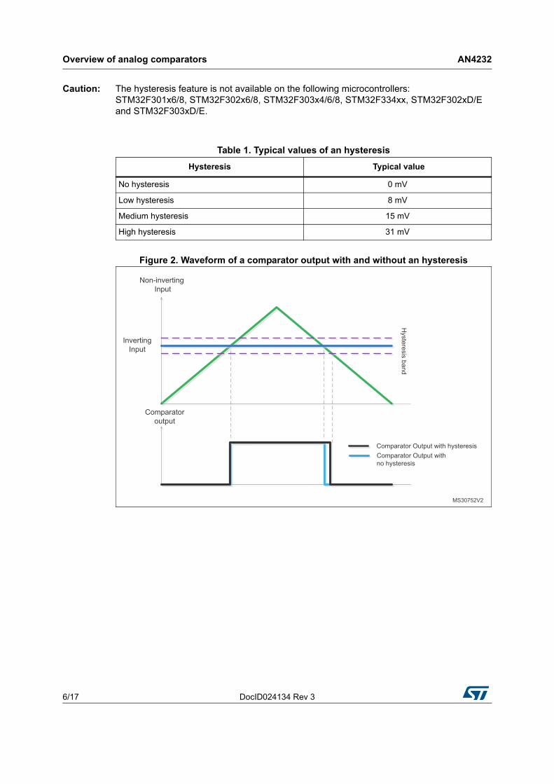
A comparator compares the inverting input with the non-inverting input and even small voltage fluctuations cause bounce on comparator the output. This bounce is not acceptable in many applications. Figure 1 shows the output bouncing when the input is noisy.
Figure 1. Effect of a noisy input on a comparator output
This bounce on the comparator output can be prevented by adding hysteresis into comparators. The analog comparators in the STM32F37x and STM32F30x devices have a configurable hysteresis value: no, low, medium and high hysteresis value. Table 1 shows the typical values of an hysteresis in each configuration.
Overview of analog comparators AN4232
6/17 DocID024134 Rev 3
Caution: The hysteresis feature is not available on the following microcontrollers: STM32F301x6/8, STM32F302x6/8, STM32F303x4/6/8, STM32F334xx, STM32F302xD/E and STM32F303xD/E.
Figure 2. Waveform of a comparator output with and without an hysteresis
Table 1. Typical values of an hysteresis
Hysteresis Typical value
No hysteresis 0 mV
Low hysteresis 8 mV
Medium hysteresis 15 mV
High hysteresis 31 mV
DocID024134 Rev 3 7/17
AN4232 Overview of analog comparators
16
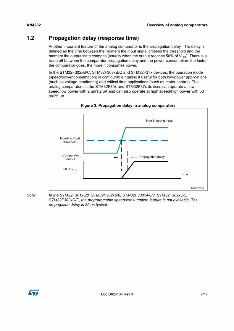
1.2 Propagation delay (response time)
Another important feature of the analog comparator is the propagation delay. This delay is defined as the time between the moment the input signal crosses the threshold and the moment the output state changes (usually when the output reaches 50% of VDD). There is a trade off between the comparator propagation delay and the power consumption: the faster the comparator goes, the more it consumes power.
In the STM32F302xB/C, STM32F303xB/C and STM32F37x devices, the operation mode (speed/power consumption) is configurable making it useful for both low-power applications (such as voltage monitoring) and critical time applications (such as motor control). The analog comparators in the STM32F30x and STM32F37x devices can operate at low speed/low power with 2 µs/1.2 µA and can also operate at high speed/high power with 50 ns/75 µA.
Figure 3. Propagation delay in analog comparators
Note: In the STM32F301x6/8, STM32F302x6/8, STM32F303x4/6/8, STM32F302xD/E STM32F303xD/E, the programmable speed/consumption feature is not available. The propagation delay is 25 ns typical.
Application examples AN4232
8/17 DocID024134 Rev 3
2 Application examples
This section describes how the analog comparators embedded in the STM32F30x and STM32F37x devices can be used in applicative examples such as humidity measurement, cycle-by-cycle motor control, voltage monitoring, and PWM control.
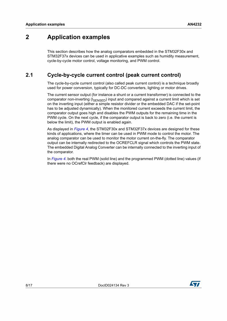
2.1 Cycle-by-cycle current control (peak current control)
The cycle-by-cycle current control (also called peak current control) is a technique broadly used for power conversion, typically for DC-DC converters, lighting or motor drives.
The current sensor output (for instance a shunt or a current transformer) is connected to the comparator non-inverting (ISENSED) input and compared against a current limit which is set on the inverting input (either a simple resistor divider or the embedded DAC if the set-point has to be adjusted dynamically). When the monitored current exceeds the current limit, the comparator output goes high and disables the PWM outputs for the remaining time in the PWM cycle. On the next cycle, if the comparator output is back to zero (i.e. the current is below the limit), the PWM output is enabled again.
As displayed in Figure 4, the STM32F30x and STM32F37x devices are designed for these kinds of applications, where the timer can be used in PWM mode to control the motor. The analog comparator can be used to monitor the motor current on-the-fly. The comparator output can be internally redirected to the OCREFCLR signal which controls the PWM state. The embedded Digital Analog Converter can be internally connected to the inverting input of the comparator.
In Figure 4. both the real PWM (solid line) and the programmed PWM (dotted line) values (if there were no OCrefClr feedback) are displayed.
DocID024134 Rev 3 9/17
AN4232 Application examples
16
Figure 4. Block diagram of cycle-by-cycle current control
Application examples AN4232
10/17 DocID024134 Rev 3
2.2 Frequency and pulse width measurement
In the STM32F30x and STM32F37x devices, the comparator output can be redirected to the input capture of the embedded timers. This feature allows a pulse width and/or frequency measurement. The input signal, whose signal width/frequency has to be measured, is connected to the non-inverting input of the analog comparator. The threshold (reference) can be powered by:
• The internal reference voltage VREFINT (1.22V) and sub-multiples (1/4 VREFINT, 1/2 VREFINT, 3/4 VREFINT)
• The embedded digital-to-analog converters
• An external pin
The comparator output is redirected internally to the input capture. In this mode, the timer counter is captured at each effective edge. When the input signal goes higher than the reference voltage, the comparator output is set to a high level generating a rising edge on the timer input capture, and the timer counter is captured in the internal register. When the input signal goes lower than the reference voltage, the comparator output is set to a low level generating a falling edge and the timer counter is captured a second time in the internal register. The time elapsed between the two consecutive captures represents the pulse width. Hence, the pulse width measurement is performed by a simple subtraction of the second and the first capture.
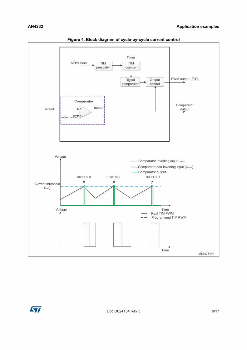
2.3 Analog voltage monitoring
The STM32F30x and STM32F37x devices embed a 12-bit analog-to-digital converter (ADC) which is very fast with a sampling rate in the order of several mega samples per second. However, with a typical consumption of 1 mA, it may not be suitable for battery-powered applications if it is left powered-on continuously. It is therefore useful to use an analog comparator in application cases where an analog voltage (sensor output) needs to be measured only when a predefined threshold is exceeded.
In the STM32F30x and STM32F37x devices, the analog comparators are designed to work even in low-power modes (Sleep mode and Stop mode). They are still powered-on and so they are able to wake-up the MCU from low-power modes. In fact, the comparator output is connected to the EXTI controller which also remains powered-on in lower-power modes.
Figure 5. Comparator output capability in low-power mode
Moreover, the comparator input is an ADC channel so PCB designer doesn't need to make an external connection between the comparator input and the ADC channel.
In an analog voltage monitoring application where the sensor output voltage is lower than the threshold, the MCU remains in Stop mode thereby saving power. As soon as the sensor output exceeds the threshold, the analog comparator wakes up the MCU, the ADC is

DocID024134 Rev 3 11/17
AN4232 Application examples
16
powered on, and the analog input voltage is measured. When the sensor output is lower than the threshold, the MCU re-enters the low-power mode to save battery life.
Enabling the ADC only when required (analog voltage higher than a threshold) dramatically reduces the average power consumption, as compared to an application where the ADC is always enabled whatever the analog voltage.
Note: When an external signal needs to be monitored within a certain voltage range or window, Window mode can be used. In this mode, the non-inverting inputs of comparators COMP1 and COMP2 are connected together and the input signal must be connected to the non-inverting input of COMP1.
In the STM32F30x devices, the Window mode is available for COMP3/COMP4 and COMP5/COMP6.
Figure 6. Current consumption in an analog voltage monitoring application
Application examples AN4232
12/17 DocID024134 Rev 3
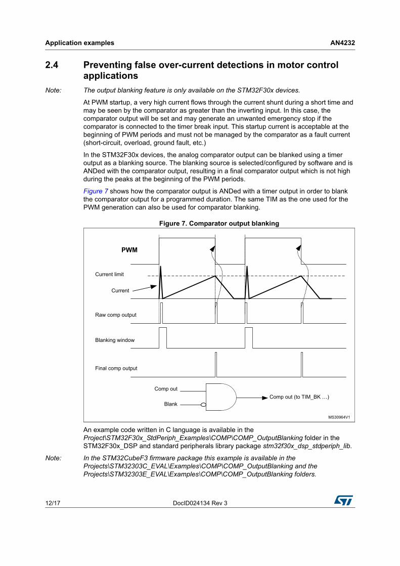
2.4 Preventing false over-current detections in motor control applications
Note: The output blanking feature is only available on the STM32F30x devices.
At PWM startup, a very high current flows through the current shunt during a short time and may be seen by the comparator as greater than the inverting input. In this case, the comparator output will be set and may generate an unwanted emergency stop if the comparator is connected to the timer break input. This startup current is acceptable at the beginning of PWM periods and must not be managed by the comparator as a fault current (short-circuit, overload, ground fault, etc.)
In the STM32F30x devices, the analog comparator output can be blanked using a timer output as a blanking source. The blanking source is selected/configured by software and is ANDed with the comparator output, resulting in a final comparator output which is not high during the peaks at the beginning of the PWM periods.
Figure 7 shows how the comparator output is ANDed with a timer output in order to blank the comparator output for a programmed duration. The same TIM as the one used for the PWM generation can also be used for comparator blanking.
Figure 7. Comparator output blanking
An example code written in C language is available in the Project\STM32F30x_StdPeriph_Examples\COMP\COMP_OutputBlanking folder in the STM32F30x_DSP and standard peripherals library package stm32f30x_dsp_stdperiph_lib.
Note: In the STM32CubeF3 firmware package this example is available in the Projects\STM32303C_EVAL\Examples\COMP\COMP_OutputBlanking and the Projects\STM32303E_EVAL\Examples\COMP\COMP_OutputBlanking folders.
DocID024134 Rev 3 13/17
AN4232 Application examples
16
The COMP_OutputBlanking example aims at showing how the blanking feature can be used.
In this example, COMP1 is configured as follows:
• The non-inverting input is connected to PA1
• The inverting input is connected to VREFINT (1.22V)
• The output is available on PA0
• The output is redirected to TIM1 BKIN to generate a break event when the non-inverting input is at a higher voltage than the inverting input (VREFINT)
• TIM1 OC5 is used as a blanking source
TIM1 is configured as follows:
• TIM1 period is APB2 clock / period = 72000000/50000 = 1440 Hz
• TIM1 CH2 (PA9) configured in PWM mode with a frequency equal to 1440 Hz and a duty cycle pulse/period = 100 * (37500/50000) = 75%
• TIM1 OC5 (internal channel: not available on GPIO) configured in PWM mode with a frequency equal to 1440 Hz and a high level equal to pulse/period = 2000/72000000 = 27.7 microseconds
• A break event is generated at a high polarity (when the non-inverting input is at a higher voltage than the inverting input)
Note: In the STM32CubeF3 firmware package this example is available in the Projects\STM32303C_EVAL\Examples\COMP\COMP_OutputBlanking and the Projects\STM32303E_EVAL\Examples\COMP\COMP_OutputBlanking folders.
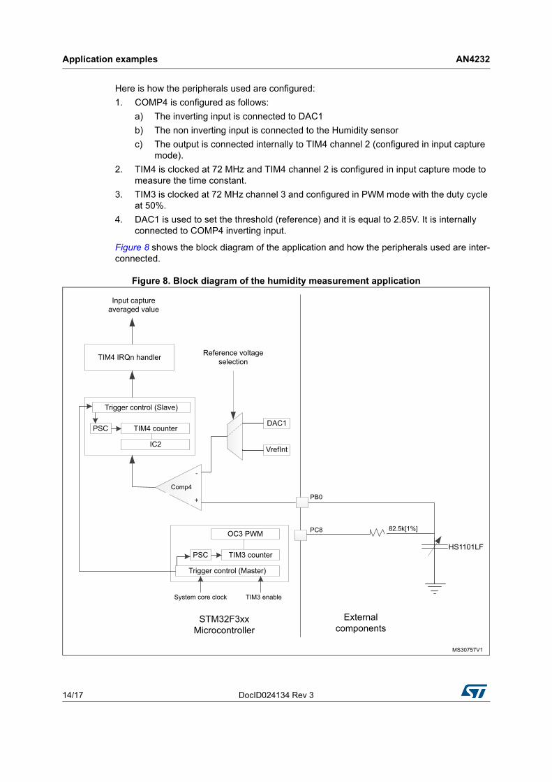
2.5 Humidity measurement
The analog comparators can be connected internally to input capture of embedded timers. This feature makes it easy to measure the capacitance values using the charge/discharge method. This “Humidity measurement” application is based on the HS1100/HS1101 capacitive relative humidity sensor available in the STM32303C-EVAL and STM32303E-EVAL evaluation boards.
Note: The application source code is available in the Project\STM32F30x_StdPeriph_Examples\ COMP\COMP_Hygrometer folder in the STM32F30x_DSP and standard peripherals library package, stm32f30x_dsp_stdperiph_lib.
In the STM32CubeF3 firmware package this example is available in the Projects\STM32303C_EVAL\Examples\COMP\COMP_Hygrometer and the Projects\STM32303E_EVAL\Examples\COMP\COMP_Hygrometer folders.
The capacitance measurement is performed using the variation of RxC time constant. A square signal generated by TIM4 is passed through a charge resistance to charge/discharge the capacitive sensor. The voltage on the sensor (Uc) is derived from the equation below:
Uc = VDD x (1–(–t/(RxC))
Where:
– VDD is the MCU power supply
– R is the charge resistance
– C is the capacitance of the sensor.
Application examples AN4232
14/17 DocID024134 Rev 3
Here is how the peripherals used are configured:
1. COMP4 is configured as follows:
a) The inverting input is connected to DAC1
b) The non inverting input is connected to the Humidity sensor
c) The output is connected internally to TIM4 channel 2 (configured in input capture mode).
2. TIM4 is clocked at 72 MHz and TIM4 channel 2 is configured in input capture mode to measure the time constant.
3. TIM3 is clocked at 72 MHz channel 3 and configured in PWM mode with the duty cycle at 50%.
4. DAC1 is used to set the threshold (reference) and it is equal to 2.85V. It is internally connected to COMP4 inverting input.
Figure 8 shows the block diagram of the application and how the peripherals used are inter-connected.
Figure 8. Block diagram of the humidity measurement application

DocID024134 Rev 3 15/17
AN4232 Application examples
16
When non-inverting COMP4 crosses the DAC1 level, the formula to compute the capacitance value is:
TriggerTime = RES * Capacitance * ln(VDD/(VDD – VREF))
where:
– TriggerTime is the time when the capture event occurred
– RES is the charge resistance. Its value is 82.5 K 1%
– Capacitance is the capacitance value of the humidity sensor
– VDD is the device power supply. It is equal to 3.3V
– VREF is the threshold generated by the DAC1
At VREF = 2.086V (generated by DAC), ln(VDD/(VDD – VREF)) is ~ 1.
Thus, the TriggerTime = RES * Capacitance, the Capacitance = TriggerTime/RES by the consequent Capacitance = (ICReadValue/SystemCoreClock)/RES
where:
– ICReadValue is the captured TIM4 counter
– SystemCoreClock is the frequency at which the device (specifically TIM3 and TIM4) is running.
Once the capacitance has been computed, the humidity value is given by:
RH (%) = -3.4656*103 * X3 + 1.0732*104 * X2 - 1.0457*104*X + 3.2459*103
where:
– X = Capacitance/Capacitance55RH
– Capacitance55RH is the capacitance at 55%.
Revision history AN4232
16/17 DocID024134 Rev 3
3 Revision history
Table 2. Document revision history
Date Revision Changes
31-Jan-2013 1 Initial release.
29-Jan-2015 2
Extended the applicability to STM32F302xD/E and STM32F303xD/E. Updated:
– Introduction
– Section 1.1: Hysteresis,
– Section 1.2: Propagation delay (response time),
– Section 2.4: Preventing false over-current detections in motor control applications
– Section 2.5: Humidity measurement
05-Jan-2017 3Updated Figure 2: Waveform of a comparator output with and without an hysteresis with the positive edge of comparator output starting at the same level with or without hysteresis.
DocID024134 Rev 3 17/17
AN4232
17
IMPORTANT NOTICE – PLEASE READ CAREFULLY
STMicroelectronics NV and its subsidiaries (“ST”) reserve the right to make changes, corrections, enhancements, modifications, and improvements to ST products and/or to this document at any time without notice. Purchasers should obtain the latest relevant information on ST products before placing orders. ST products are sold pursuant to ST’s terms and conditions of sale in place at the time of order acknowledgement.
Purchasers are solely responsible for the choice, selection, and use of ST products and ST assumes no liability for application assistance or the design of Purchasers’ products.
No license, express or implied, to any intellectual property right is granted by ST herein.
Resale of ST products with provisions different from the information set forth herein shall void any warranty granted by ST for such product.
ST and the ST logo are trademarks of ST. All other product or service names are the property of their respective owners.
Information in this document supersedes and replaces information previously supplied in any prior versions of this document.
© 2017 STMicroelectronics – All rights reserved