Embed Size (px)
Citation preview

Analog Design Methodology
Perry L Heedley, Ph.D.Kenneth C Dyer, Ph.D.
Patrick Isakanian

Outline
• Overview of Analog Design Methodology
• Phases in an Analog Design– Architecture Phase– Preliminary Design Phase– Layout Phase– Final Design Phase
• Final Thoughts
• Appendix A: Checklists for each review

Overview of Analog Design Methodology
• Characteristics of a good analog design methodology :– Starts with a through literature review to understand previous work– Is broken into several phases, with peer reviews for each to allow
“mid-course corrections” before going too far down the wrong path
• Design Phases :– Architecture Phase – determine what needs to be built– Preliminary Design Phase – do initial design & get ready for layout– Layout Phase – create the preliminary layout– Final Design Phase – simulate with parasitics & finish the design

Overview of Analog Design Methodology
• Key points to remember :– Analog design & layout is an iterative process!
(e.g., layout “tweaks” are typically required after simswith extracted parasitics)
– Think before just jumping in! Designing the wrong thing wastes both your time and the time of others, and may delay the chip
“We pay you to think, not just push transistors!”– Eric Swanson, former Crystal Semiconductor CTO

Purpose & Goals of the Architecture Phase
• The Purpose of the Architecture Phase is to :– Understand what you need to build to solve the problem– Find out how similar problems have been solved in the past– Examine tradeoffs between competing solutions– Identify any possible “show stopper” issues before design begins
• The Goals of the Architecture Phase are to :– Resolve any open issues that could affect your design– Decide exactly what it is that you plan to build in the
Preliminary Design Phase
Completing the design is not the goal of this phase!

Architecture Phase Tasks
• Perform a good literature review to understand :– What is the state-of-the-art for this type of circuit ?– What level of performance is possible in my process ?– What specs/tradeoffs are important to consider ?– What proven circuit topologies have been used in the past
to successfully solve this problem? (or similar problems)
• Decide where innovation is required– What are the new “value added” portions of your design?
• Understand what makes your chip better than the competition,and focus on that !
– What parts of your design can be borrowed from previous work?• Avoid “NIH” (Not Invented Here) thinking and re-inventing the wheel
– Innovation brings risk, so innovate only where required!
“You tried too many new things on that chip for it to work.”– Nav Sooch, Silicon Labs founder & CEO

Architecture Phase Tasks
• Identify opportunities for reuse– e.g., can you build 1 op amp and use it in several places instead
of having to design & layout multiple op amps?
• Decide exactly what it is that you plan to build in the Preliminary Design Phase– All block architectures & circuit topologies are determined
• e.g., an interpolating flash or a sub-ranging ADC ?Interpolate by 2 or by 4 ?
– All required specs are determined• e.g., required speed and effective number of bits for an ADC ?
– All or most test modes have been identified and considered• It is usually easier and quicker to “build in” a test mode during
design than to add it later as an after thought

What an Architecture Review should cover
• Summary of all required specifications• Comparison of all architectures considered
– Compare the pros & cons of each– Explain which architecture was chosen and why– Show any simulations run to confirm the choice of architecture
• Overview of what you plan to build– Block diagrams or preliminary schematics, as appropriate– Details for all specs needed to begin the design (e.g., sub-blocks)– Summary of any test modes or other special modes planned– Interface information needed by other blocks and/or top level
• I/O signals, clocks and power supplies required, etc.
The goal is to show that the architectureselected should meet all requirements!

Purpose & Goals of the Preliminary Design Phase
• The Purpose of the Preliminary Design Phase is to :– Design any new circuits required– Verify the performance of any “borrowed” circuits in your application– Solve any known issues and flush out new ones– Show that your design meets all specs, including additional margin
to account for expected layout parasitics– Get ready for layout to start
• The Goals of the Preliminary Design Phase are to :– Complete your design to the point where it is ready to enter layout,
not to completely polish and finish the design!– Develop a layout floorplan for your block
• Aspect ratio, signal & power supply routing, device placement, etc.

Preliminary Design Phase Tasks
• Design any new circuits, down to the transistor level– Develop all needed test benches for simulations, including detailed
models for sources and loads– Run simulations to show all specs are met, with extra margin
for expected layout parasitics– Simulate over all standard corner cases defined for the chip, (e.g.,
process, temperature, supply voltage) plus any additional corners which could cause problems for this specific circuit
• Verify the performance of any “borrowed” circuits– Be sure that you understand the circuit, including any known issues– Run any sims needed to verify performance in your application
• A complete set of corner sims may not be needed, depending on the status of the block (e.g., has it already been proven in silicon?)
• Check the interfaces to your other blocks, plus any control signals• Be sure to exercise any unusual modes of operation being used
Preliminary Design Phase Tasks
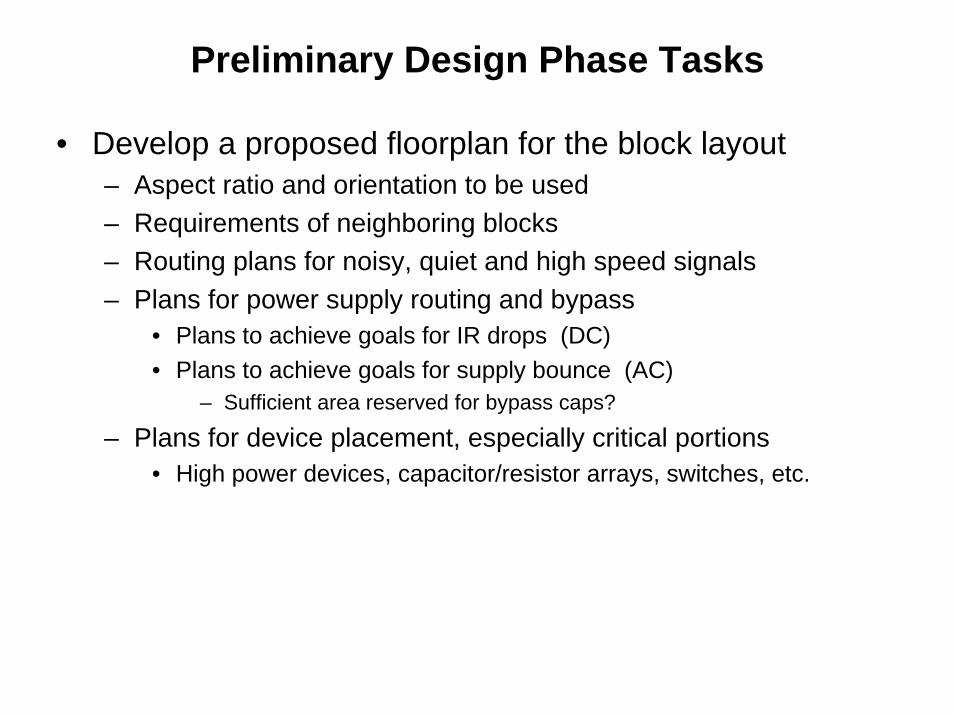
• Develop a proposed floorplan for the block layout– Aspect ratio and orientation to be used– Requirements of neighboring blocks– Routing plans for noisy, quiet and high speed signals– Plans for power supply routing and bypass
• Plans to achieve goals for IR drops (DC)• Plans to achieve goals for supply bounce (AC)
– Sufficient area reserved for bypass caps?
– Plans for device placement, especially critical portions• High power devices, capacitor/resistor arrays, switches, etc.
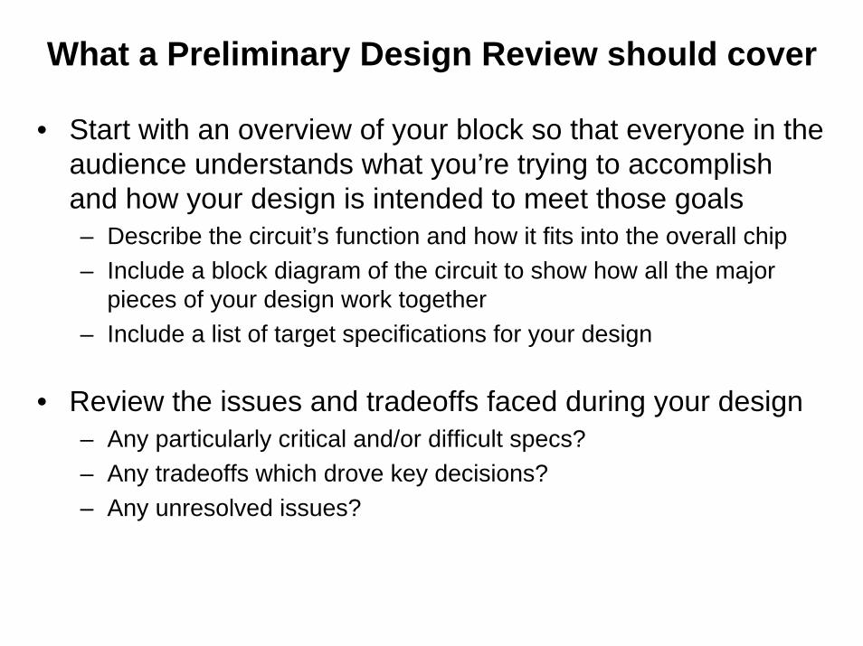
What a Preliminary Design Review should cover
• Start with an overview of your block so that everyone in the audience understands what you’re trying to accomplish and how your design is intended to meet those goals– Describe the circuit’s function and how it fits into the overall chip– Include a block diagram of the circuit to show how all the major
pieces of your design work together– Include a list of target specifications for your design
• Review the issues and tradeoffs faced during your design– Any particularly critical and/or difficult specs?– Any tradeoffs which drove key decisions?– Any unresolved issues?

What a Preliminary Design Review should cover
• Review all the schematics used in your design– Include a complete set of schematics for your design, taking care
that all important details (e.g., W/L ratios) are clearly visible– Discuss how the circuits work together, from a top down perspective– Describe in detail how each circuit works, including the purpose of
all transistors used, devices requiring good matching, etc.– Discuss any interactions between devices, critical issues, etc. which
drove decisions in your design
• Show simulation results to prove the design meets all specs– Include sims for all block specifications– Include sims over all standard corners defined by the project lead– Include sims for any special corners or tests required for this block– Be sure that all plots communicate the desired information clearly
• Titles on all plots? Are all axes labeled? All curves clearly visible?

What a Preliminary Design Review should cover
• Show your proposed layout floorplan for the block– How will this block fit into the overall chip?
• aspect ratio, connections to neighboring blocks, etc.– Location of all major sub-blocks in your design
• op amps, capacitor/resistor arrays, switch arrays, etc.– Routing of power & ground to/from/through the block– Location of any quiet, noisy and high speed wiring channels
• Routing of inputs and outputs, clocks, bias & control signals, etc.• Any dedicated and/or shielded wiring channels?
– Any special considerations?• e.g., placement of sensitive devices, signals, etc.,
relative to any nearby noisy circuits?• Deep Nwell, and/or guard rings used to reduce noise?• Location and size of bypass capacitors?
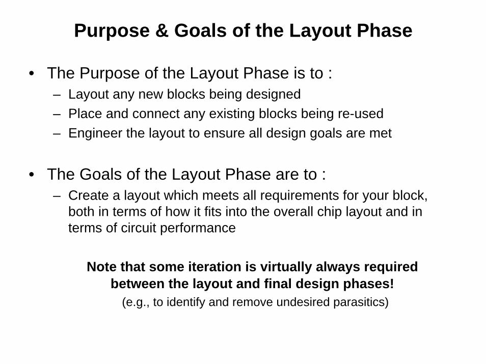
Purpose & Goals of the Layout Phase
• The Purpose of the Layout Phase is to :– Layout any new blocks being designed– Place and connect any existing blocks being re-used– Engineer the layout to ensure all design goals are met
• The Goals of the Layout Phase are to :– Create a layout which meets all requirements for your block,
both in terms of how it fits into the overall chip layout and interms of circuit performance
Note that some iteration is virtually always requiredbetween the layout and final design phases!
(e.g., to identify and remove undesired parasitics)
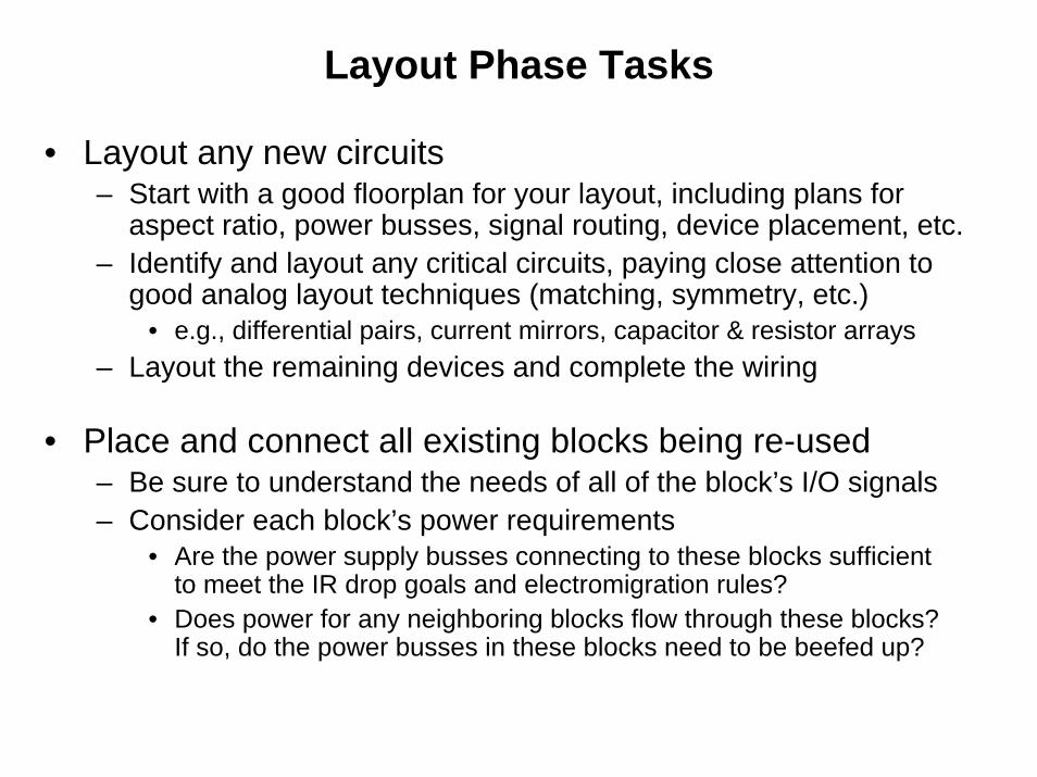
Layout Phase Tasks
• Layout any new circuits– Start with a good floorplan for your layout, including plans for
aspect ratio, power busses, signal routing, device placement, etc.– Identify and layout any critical circuits, paying close attention to
good analog layout techniques (matching, symmetry, etc.)• e.g., differential pairs, current mirrors, capacitor & resistor arrays
– Layout the remaining devices and complete the wiring
• Place and connect all existing blocks being re-used– Be sure to understand the needs of all of the block’s I/O signals– Consider each block’s power requirements
• Are the power supply busses connecting to these blocks sufficientto meet the IR drop goals and electromigration rules?
• Does power for any neighboring blocks flow through these blocks?If so, do the power busses in these blocks need to be beefed up?

Layout Phase Tasks
• Consider any special requirements – For blocks connected to I/O pads: ESD, Latchup– Test-mode requirements: bypass modes, routing of test busses,
getting high speed signals off-chip cleanly, etc.
• Once the block passes all rule checks (DRC, LVS, etc.) plus visual inspection for matching, symmetry, etc., then run parasitic extraction on the block and begin simulations with parasitics (Final Design Phase)– This step typically requires iteration between simulations and layout
changes, as coupling & loading problems are found and corrected

What a Layout Review should cover
• The goal of the Layout Review is to carefully inspect the block’s layout for any problems or issues that can be detected visually. Examples include non-symmetrical routing of differential signals, unintended coupling between wires, poor power bus routing, lack of symmetry in device arrays, etc.
Note that this review is critical, since these types of issuesare NOT detected by automated checks such as DRC & LVS!

What a Layout Review should cover
• Start with one or more large plots of the block’s layout,preferably plotted to scale (e.g., 1000x) for ease in making measurements on the plot(s)– For large blocks, it is often best to use a zoomed-out plot of the
entire layout combined with several plots which are zoomed-in tightly on critical portions of the layout
– Use a CAD layout editor to zoom/highlight critical layers
• Have a complete set of schematics on hand for use by those reviewing the plot(s), so that they can understand the circuits involved
• Be sure to check :– Routing of critical signals for symmetry, coupling, shielding, etc.– Placement and hook-up of matched devices, resistor & cap arrays– Power bus routing and current carrying capacity

Purpose & Goals of the Final Design Phase
• The Purpose of the Final Design Phase is to :– Identify and correct any problems in the block’s layout which
could cause performance problems• e.g., unintended coupling between signals, too much capacitive
loading on a node, lack of symmetry on differential signals, etc.
• The Goals of the Final Design Phase are to :– Complete the circuit design & layout and ensure that the final
design meets all specifications, including layout parasitics
Note that some iteration is virtually always requiredbetween the layout and final design phases!
(e.g., to identify and remove undesired parasitics)

Final Design Phase Tasks
• Repeat all simulations run during the Preliminary Design Phase, using the netlist extracted from the layout
• Check to make sure that all specifications are still met, including layout parasitics
• Finalize the design for Tapeout

What a Final Design Review should cover
• A brief review of the block’s function, architecture and circuitdesign, to refresh the audience– Typically a sub-set of material from the Preliminary Design Review
• A description of all changes made since the PDR
• Show simulation results to prove the design meets all specs– Include sims for all block specifications– Include sims over all standard corners defined by the project lead– Include sims for any special corners or tests required for this block– Be sure that all plots communicate the desired information clearly
• Titles on all plots? Are all axes labeled? All curves clearly visible?

Final Thoughts
• You are a CHIP designer, not a block designer
• Getting working silicon into customer’s hands in the shortest possible time is the ultimate goal
• Sometimes you need to slow down in order to speed up– A few extra weeks in design time can save you many months
in debug time!– You always pay for risks and “cutting corners” somehow
• poor circuit performance, excess debug time,additional silicon revisions…
Proceeding with “all deliberate speed” usually wins!

Appendix A
Checklists for each review
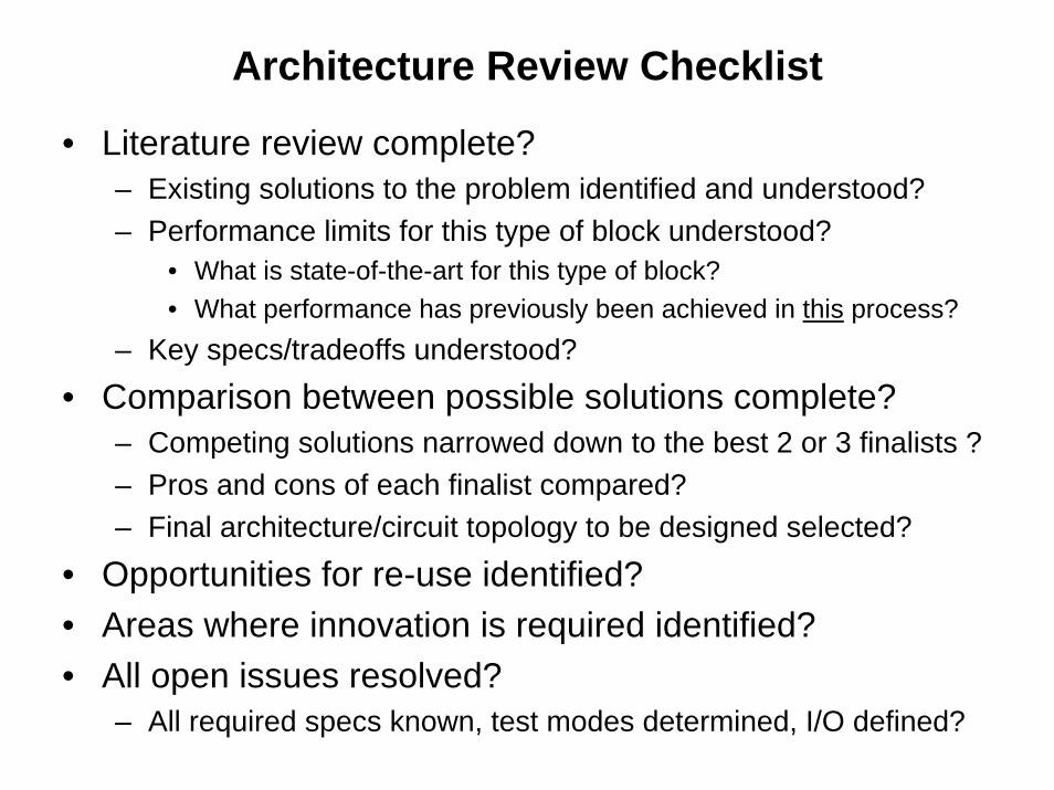
Architecture Review Checklist
• Literature review complete?– Existing solutions to the problem identified and understood?– Performance limits for this type of block understood?
• What is state-of-the-art for this type of block?• What performance has previously been achieved in this process?
– Key specs/tradeoffs understood?
• Comparison between possible solutions complete?– Competing solutions narrowed down to the best 2 or 3 finalists ?– Pros and cons of each finalist compared?– Final architecture/circuit topology to be designed selected?
• Opportunities for re-use identified?• Areas where innovation is required identified?• All open issues resolved?
– All required specs known, test modes determined, I/O defined?

Preliminary Design Review Checklist
• Overview of the block’s function & specs included?• Description of any key specs/tradeoffs included?• Schematics for all circuits included?• All simulations complete and plots clearly showing the
results achieved included?– Sims run to show that all specifications are met?– Sims run over all standard corners (process/supply/temp)?– Sims run over any special corners needed for this block?– Sims run to verify the performance of any borrowed blocks?– All sims include accurate models for loads & sources?
• Floorplan for layout complete?– Aspect ratio, orientation, needs of neighboring blocks defined?– Plans for routing of noisy, quiet & high speed signals complete?– Plans for routing of power supplies and bypass caps complete?– Plans for device placement complete?

Layout Review Checklist
• Are all new block layouts complete?– Are all layout flows passing? (DRC, LVS, ANT, density, etc.?)– Are all critical devices laid out to meet their matching goals?
• All diff pairs, current sources and cap/resistor arrays checked?• All guidelines for symmetry, centroding, dummies met?
– Are all signals routed properly?• Quiet and noisy signals separated and/or shielded?• Good symmetry used on all differential signals?• Low capacitance routes achieved on all high speed signals?
– Supply busses meet IR drop goals and electromigration rules?– Adequate bypass caps included to meet supply bounce goals?
• Have all blocks being reused been connected properly?– All I/O signals, supplies, etc. checked?

Final Design Review Checklist
• Brief review of the block’s function and specs included to refresh your audience?
• Description of any key specs/tradeoffs included?• Description of all changes made since the PDR included?• Are all final simulations including parasitics complete?
– Sims run to show that all specifications are met?– Sims run over all standard corners (process/supply/temp)?– Sims run over any special corners needed for this block?– Sims run to verify the performance of any “borrowed” blocks?– All sims include accurate models for loads & sources?

Appendix B
Examples of Good and BadSimulation Plots & Schematics

Example of too many curves on one plot
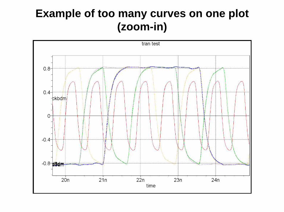
Example of too many curves on one plot(zoom-in)

Example of using strips to make plots readable

Example of using strips to make plots readable(zoom-in)

Example of plot too zoomed out to show details

Example of problem with plots showingall single-ended signals

Example of clarity gained by plottingdifferential signals

Example of clarity gained by plottingcommon-mode signals
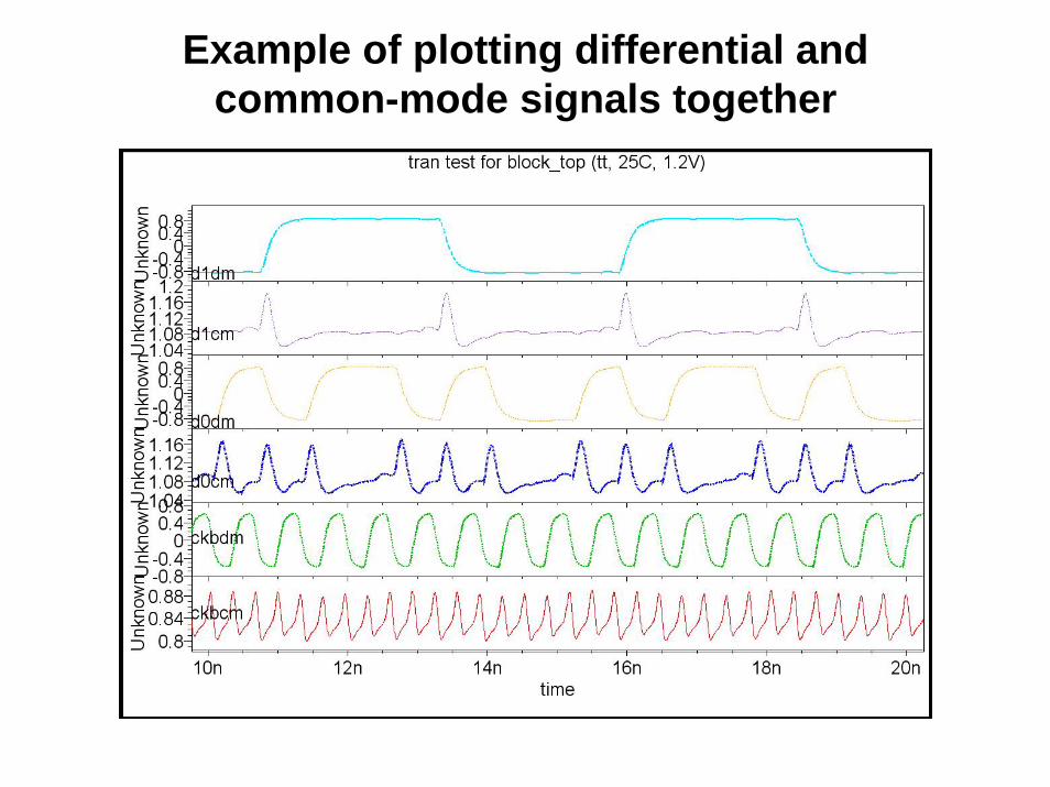
Example of plotting differential andcommon-mode signals together