Embed Size (px)
Citation preview
Analyzing 26-53 GBaud PAM4 Optical and Electrical Signals––APPLICATION NOTE
2 | WWW.TEK.COM
APPLICATION NOTEAnalyzing 26-53 GBaud PAM4 Optical and Electrical Signals
Contents
1. Introduction ................................................................................. 3
2. Current PAM4 Technologies .................................................. 4
3. Debugging PAM4 Systems and Transceivers ............... 7
3.1 Test setup and concepts ..........................................7
3.2 The role of reference receivers in debug
testing and compliance measurements ...................8
3.3 Error navigation ......................................................10
3.4 Test patterns ...........................................................11
4. Analyzing PAM4 Signals ......................................................12
4.1 PAM4 versions of OMA and ER .............................12
4.2 TDECQ—Transmitter and Dispersion Eye
Closure Quaternary ................................................13
4.3 Transition Time .......................................................15
4.4 EH and EW—Eye Height and Eye Width ................16
4.5 SNDR—Signal to Noise and Distortion Ratio .........17
4.6 Level Separation Mismatch Ratio—RLM ...............18
4.7 ESMW—Eye Symmetry Mask Width .....................19
5. Critical Test Equipment Requirements ...........................20
WWW.TEK.COM | 3
APPLICATION NOTEAnalyzing 26-53 GBaud PAM4 Optical and Electrical Signals
1. IntroductionPAM4 (4-level pulse amplitude modulation) is being adopted
in many applications at data rates of 50 Gb/s and higher. By
encoding two bits in each symbol, PAM4 signals use half the
bandwidth of the logic-emulating NRZ (non-return to zero)
modulation scheme to transmit at the same data rate.
Operating at half the bandwidth sidesteps the crippling effects
of loss and inter-symbol interference caused by nonuniform
channel frequency response, but the advantages of PAM4
come at a cost: the complexities of a four level system, 12
different symbol transitions, each with its own slew rate, and a
drop in SNR (signal to noise ratio) of at least a factor of three,
9.5 dB for electrical voltage and 4.7 dB for optical power.
The dramatic SNR drop is addressed in most cases by
the introduction of forward error correction. FEC provides
the performance margin necessary to raise the maximum
permitted raw BER (bit error ratio) from 1E-12 to 2.4E-4.
At such high BERs, real time oscilloscopes are capable of
measuring BER without approximation or extrapolation—
terrain that used to be reserved for expensive and inflexible
BERTs (BER testers).
This paper presents techniques for analyzing 50+ Gb/s optical
and electrical PAM4 signals. Drawing primarily from the
latest emerging technologies, 50/100/200/400 GbE (gigabit
Ethernet, IEEE 802.3bs and 802.3cd) and OIF-CEI 4.0 (Optical
Internetworking Forum-Common Electrical Interface), we’ll look
at signal analysis from the perspectives of compliance and
debug testing for both components and systems.
In the next section we give a brief summary of PAM4 standards
and their topologies. Section 3 discusses test configurations
for debugging optical and electrical signals. In Section 4, we
work through the key PAM4 optical and electrical compliance
tests and conclude in Section 5 with a summary of the test
equipment features and requirements that you need to debug
PAM4 transceivers and perform standards compliance tests.
4 | WWW.TEK.COM
APPLICATION NOTEAnalyzing 26-53 GBaud PAM4 Optical and Electrical Signals
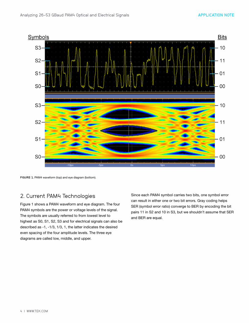
2. Current PAM4 TechnologiesFigure 1 shows a PAM4 waveform and eye diagram. The four
PAM4 symbols are the power or voltage levels of the signal.
The symbols are usually referred to from lowest level to
highest as S0, S1, S2, S3 and for electrical signals can also be
described as -1, -1/3, 1/3, 1, the latter indicates the desired
even spacing of the four amplitude levels. The three eye
diagrams are called low, middle, and upper.
Since each PAM4 symbol carries two bits, one symbol error
can result in either one or two bit errors. Gray coding helps
SER (symbol error ratio) converge to BER by encoding the bit
pairs 11 in S2 and 10 in S3, but we shouldn’t assume that SER
and BER are equal.
FIGURE 1. PAM4 waveform (top) and eye diagram (bottom).
WWW.TEK.COM | 5
APPLICATION NOTEAnalyzing 26-53 GBaud PAM4 Optical and Electrical Signals
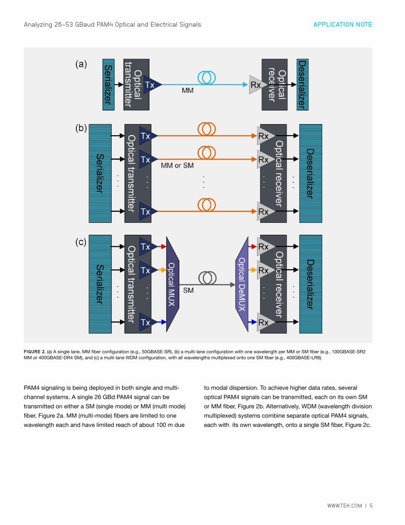
PAM4 signaling is being deployed in both single and multi-
channel systems. A single 26 GBd PAM4 signal can be
transmitted on either a SM (single mode) or MM (multi mode)
fiber, Figure 2a. MM (multi-mode) fibers are limited to one
wavelength each and have limited reach of about 100 m due
to modal dispersion. To achieve higher data rates, several
optical PAM4 signals can be transmitted, each on its own SM
or MM fiber, Figure 2b. Alternatively, WDM (wavelength division
multiplexed) systems combine separate optical PAM4 signals,
each with its own wavelength, onto a single SM fiber, Figure 2c.
FIGURE 2. (a) A single lane, MM fiber configuration (e.g., 50GBASE-SR), (b) a multi-lane configuration with one wavelength per MM or SM fiber (e.g., 100GBASE-SR2 MM or 400GBASE-DR4 SM), and (c) a multi-lane WDM configuration, with all wavelengths multiplexed onto one SM fiber (e.g., 400GBASE-LR8).
6 | WWW.TEK.COM
APPLICATION NOTEAnalyzing 26-53 GBaud PAM4 Optical and Electrical Signals
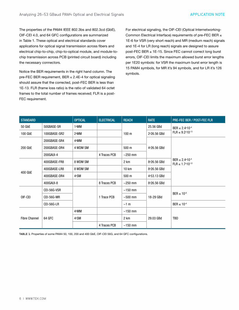
TABLE 1. Properties of some PAM4 50, 100, 200 and 400 GbE, OIF-CEI 56G, and 64 GFC configurations.
STANDARD OPTICAL ELECTRICAL REACH RATE PRE-FEC BER / POST-FEC FLR
50 GbE 50GBASE-SR 1•MM
100 m
25.56 GBd BER ≤ 2.4•10-4
FLR ≤ 9.2•10-13100 GbE 100GBASE-SR2 2•MM 2•26.56 GBd
200 GbE
200GBASE-SR4 4•MM
4•26.56 GBd
BER ≤ 2.4•10-4
FLR ≤ 1.7•10-12
200GBASE-DR4 4 WDM SM 500 m
200GAUI-4 4 Traces PCB ~250 mm
400 GbE
400GBASE-FR8 8 WDM SM 2 km 8•26.56 GBd
400GBASE-LR8 8 WDM SM 10 km 8•26.56 GBd
400GBASE-DR4 4•SM 500 m 4•53.13 GBd
400GAUI-8 8 Traces PCB ~250 mm 8•26.56 GBd
OIF-CEI
CEI-56G-VSR
1 Trace PCB
~150 mm
18-29 GBdBER ≤ 10-6
CEI-56G-MR ~500 mm
CEI-56G-LR ~1 m BER ≤ 10-4
Fibre Channel 64 GFC
4•MM ~150 mm
29.03 GBd TBD4•SM 2 km
4 Traces PCB ~150 mm
The properties of the PAM4 IEEE 802.3bs and 802.3cd (GbE),
OIF-CEI 4.0, and 64 GFC configurations are summarized
in Table 1. These optical and electrical standards cover
applications for optical signal transmission across fibers and
electrical chip-to-chip, chip-to-optical module, and module-to-
chip transmission across PCB (printed circuit board) including
the necessary connectors.
Notice the BER requirements in the right hand column. The
pre-FEC BER requirement, BER ≤ 2.4E-4 for optical signaling
should assure that the corrected, post-FEC BER is less than
1E-13. FLR (frame loss ratio) is the ratio of validated 64 octet
frames to the total number of frames received; FLR is a post-
FEC requirement.
For electrical signaling, the OIF-CEI (Optical Internetworking-
Common Electrical Interface) requirements of pre-FEC BER ≤
1E-6 for VSR (very short reach) and MR (medium reach) signals
and 1E-4 for LR (long reach) signals are designed to assure
post-FEC BER ≤ 1E-15. Since FEC cannot correct long burst
errors, OIF-CEI limits the maximum allowed burst error lengths
per 1E20 symbols: for VSR the maximum burst error length is
15 PAM4 symbols, for MR it’s 94 symbols, and for LR it’s 126
symbols.
WWW.TEK.COM | 7
APPLICATION NOTEAnalyzing 26-53 GBaud PAM4 Optical and Electrical Signals
3. Debugging PAM4 Systems and Transceivers Testing a transceiver for compliance to the specified
requirements of a technology standard should assure that
any signal that it transmits will be interoperable with any
combination of other compliant channels and transceivers.
Diagnostic or debug testing, on the other hand, uncovers
the flaws that cause transceivers to malfunction or fail a
compliance test.
One key difference between compliance testing and diagnostic
testing is that compliance tests challenge the signal in a
representative environment with a stressful test pattern, all
channels turned on to generate maximum crosstalk, and the
signal transmitted through a compliance test fiber or channel.
In diagnostic testing it’s helpful to start with simple conditions
to get everything working before introducing increasingly
stressful patterns, channels, and crosstalk first separately and
then together until we find the problem.
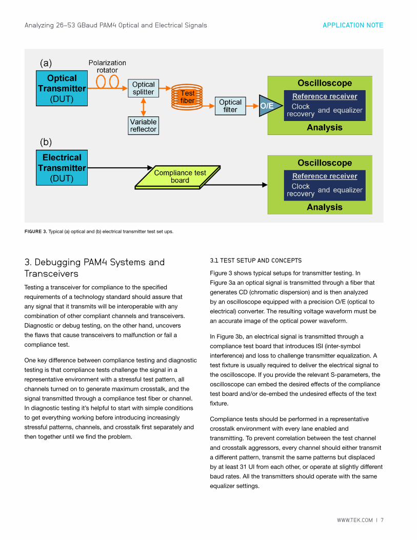
3.1 TEST SETUP AND CONCEPTS
Figure 3 shows typical setups for transmitter testing. In
Figure 3a an optical signal is transmitted through a fiber that
generates CD (chromatic dispersion) and is then analyzed
by an oscilloscope equipped with a precision O/E (optical to
electrical) converter. The resulting voltage waveform must be
an accurate image of the optical power waveform.
In Figure 3b, an electrical signal is transmitted through a
compliance test board that introduces ISI (inter-symbol
interference) and loss to challenge transmitter equalization. A
test fixture is usually required to deliver the electrical signal to
the oscilloscope. If you provide the relevant S-parameters, the
oscilloscope can embed the desired effects of the compliance
test board and/or de-embed the undesired effects of the text
fixture.
Compliance tests should be performed in a representative
crosstalk environment with every lane enabled and
transmitting. To prevent correlation between the test channel
and crosstalk aggressors, every channel should either transmit
a different pattern, transmit the same patterns but displaced
by at least 31 UI from each other, or operate at slightly different
baud rates. All the transmitters should operate with the same
equalizer settings.
FIGURE 3. Typical (a) optical and (b) electrical transmitter test set ups.
8 | WWW.TEK.COM
APPLICATION NOTEAnalyzing 26-53 GBaud PAM4 Optical and Electrical Signals
3.2 THE ROLE OF REFERENCE RECEIVERS IN DEBUG TESTING AND COMPLIANCE MEASUREMENTS
The oscilloscope serves as both test instrument and reference
receiver in the transmitter test configurations shown in Figure
3. The ability of high performance real time oscilloscopes
to replicate the performance of almost any receiver without
additional hardware makes them flexible enough to perform
a huge variety of debug tests as well as the most complex
compliance measurements—provided that the scope has a low
noise floor, appropriate bandwidth for the application, sufficient
memory depth, and for optical measurements, a linear, low
noise O/E convertor.
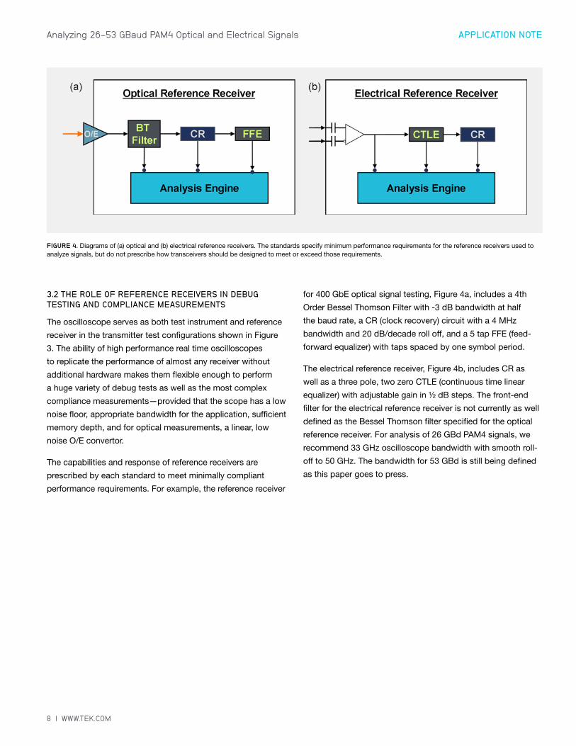
The capabilities and response of reference receivers are
prescribed by each standard to meet minimally compliant
performance requirements. For example, the reference receiver
for 400 GbE optical signal testing, Figure 4a, includes a 4th
Order Bessel Thomson Filter with -3 dB bandwidth at half
the baud rate, a CR (clock recovery) circuit with a 4 MHz
bandwidth and 20 dB/decade roll off, and a 5 tap FFE (feed-
forward equalizer) with taps spaced by one symbol period.
The electrical reference receiver, Figure 4b, includes CR as
well as a three pole, two zero CTLE (continuous time linear
equalizer) with adjustable gain in ½ dB steps. The front-end
filter for the electrical reference receiver is not currently as well
defined as the Bessel Thomson filter specified for the optical
reference receiver. For analysis of 26 GBd PAM4 signals, we
recommend 33 GHz oscilloscope bandwidth with smooth roll-
off to 50 GHz. The bandwidth for 53 GBd is still being defined
as this paper goes to press.
FIGURE 4. Diagrams of (a) optical and (b) electrical reference receivers. The standards specify minimum performance requirements for the reference receivers used to analyze signals, but do not prescribe how transceivers should be designed to meet or exceed those requirements.
WWW.TEK.COM | 9
APPLICATION NOTEAnalyzing 26-53 GBaud PAM4 Optical and Electrical Signals
While the standards prescribe the reference receiver’s minimal
performance, they do not prescribe how actual receivers
should achieve that performance. Actual PAM4 transceiver
and SerDes implementations often use proprietary analog
or DSP (digital signal processing) techniques that surpass
the minimally compliant filtering, CR, and equalization
requirements of reference receivers.
By using a real time oscilloscope, you can experiment with
different receiver designs.
For example, recovering a data-rate clock from an impaired
PAM4 signal is more difficult than CR from an NRZ signal. The
clock is recovered from the timing of signal transitions; the
cleaner the transition, the more seamless the CR. While every
NRZ transition swings between the minimum and maximum
power or voltage levels, just 1/6 of PAM4 transitions swing
between S0 and S3; half of PAM4 signal transitions span
just 1/3 of the peak-to-peak levels. Using built-in algorithms
through a straightforward user interface, you can easily
configure PLL (phase-locked loop) or DSP-based CR designs
and find ways to recover clocks from even highly impaired
signals. You can then view the signal with the extracted clock
or export the waveforms for offline analysis.
Similarly, you can experiment with different equalization
schemes, analyze signals before and after equalization,
determine the best eye-opening gain for your CTLE, the best
taps for your FFE, and determine whether DFE (decision
feedback equalization) is suitable for your design.
DFE is largely being replaced in electrical receivers by CTLE or
both CTLE and receiver FFE. DFE was one of the innovations
that enabled NRZ designs to achieve multi-gigabit data rates,
but it is subject to burst errors. The Reed Solomon FEC
schemes used in most PAM4 applications can accommodate
burst errors of 30 bits without a problem, but with a pre-FEC
BER of 1E-6, FEC failure can be problematic. On the other
hand, with four “decisions” to “feedback,” PAM4 DFE has
potential. Choosing whether or not to use DFE in a receiver
requires careful analysis.
10 | WWW.TEK.COM
APPLICATION NOTEAnalyzing 26-53 GBaud PAM4 Optical and Electrical Signals
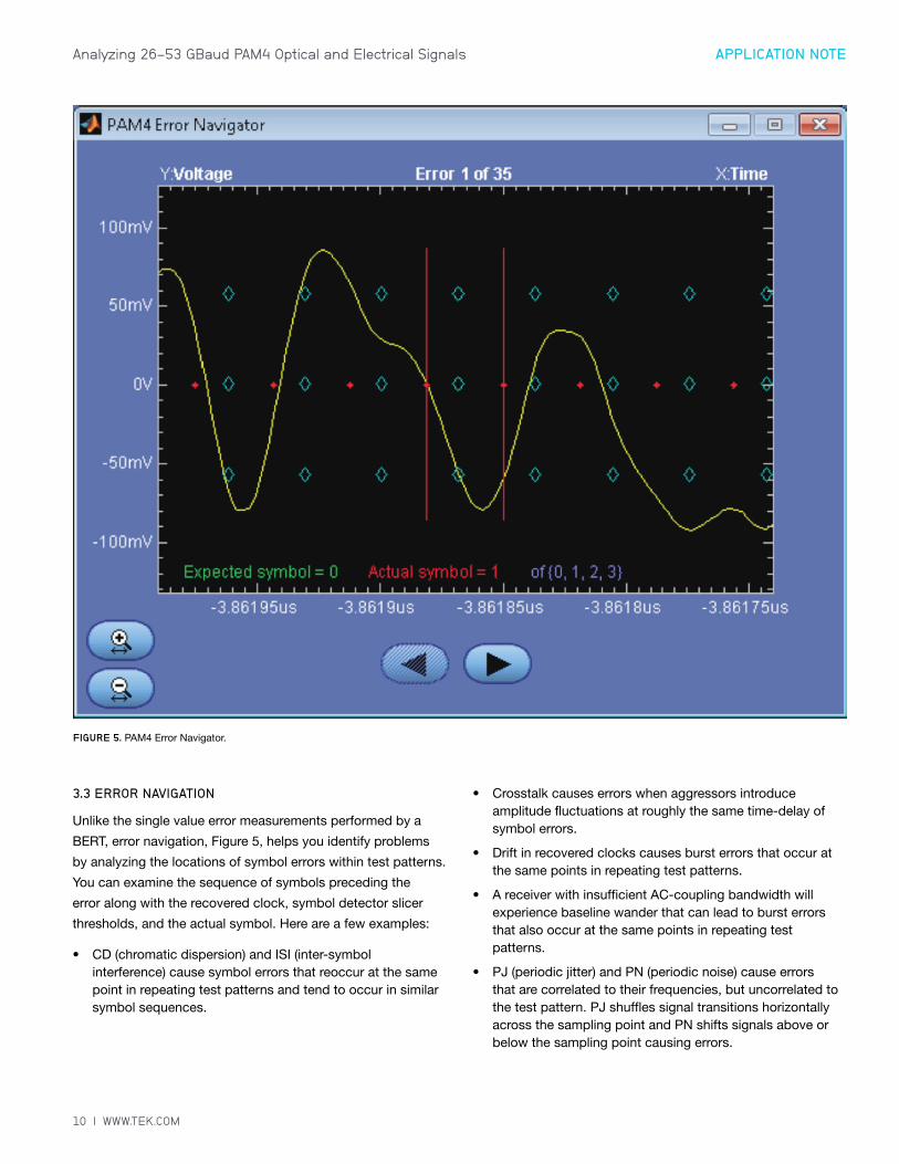
3.3 ERROR NAVIGATION
Unlike the single value error measurements performed by a
BERT, error navigation, Figure 5, helps you identify problems
by analyzing the locations of symbol errors within test patterns.
You can examine the sequence of symbols preceding the
error along with the recovered clock, symbol detector slicer
thresholds, and the actual symbol. Here are a few examples:
• CD (chromatic dispersion) and ISI (inter-symbol interference) cause symbol errors that reoccur at the same point in repeating test patterns and tend to occur in similar symbol sequences.
• Crosstalk causes errors when aggressors introduce amplitude fluctuations at roughly the same time-delay of symbol errors.
• Drift in recovered clocks causes burst errors that occur at the same points in repeating test patterns.
• A receiver with insufficient AC-coupling bandwidth will experience baseline wander that can lead to burst errors that also occur at the same points in repeating test patterns.
• PJ (periodic jitter) and PN (periodic noise) cause errors that are correlated to their frequencies, but uncorrelated to the test pattern. PJ shuffles signal transitions horizontally across the sampling point and PN shifts signals above or below the sampling point causing errors.
FIGURE 5. PAM4 Error Navigator.
WWW.TEK.COM | 11
APPLICATION NOTEAnalyzing 26-53 GBaud PAM4 Optical and Electrical Signals
3.4 TEST PATTERNS
The five test patterns in Table 2 are used for compliance
testing but also serve most diagnostic test needs. PRBSnQ
(pseudo-random binary sequence n quaternary) patterns are
derived from the corresponding binary PRBSn patterns. The
quaternary version, PRBSnQ, is derived by Gray coding bits
from repetitions of the binary PRBSn pattern into the MSB
(most significant bit) and LSB (least significant bit) of PAM4
symbols. Just as a PRBSn pattern consists of 2n-1 bits, the
PRBSnQ consists of 2n-1 PAM4 symbols.
The simplest of the standard test patterns, the square wave
composed of alternating runs of 8 consecutive S3 and S0
symbols is used in tests that concentrate on the power or
voltage levels of the signal rails. PRBS13Q is used in most
transmitter tests and PRBS31Q is used in most receiver
tests. Since PRBS13Q consists of just 8191 symbols, it’s
short enough for several repetitions of the waveform to be
captured by an oscilloscope. With many repetitions, exhaustive
signal analysis can be performed: signal impairments that are
correlated or uncorrelated to the pattern can be separated,
random jitter and noise can be measured, periodic jitter and
noise can be identified and distinguished from crosstalk,
and so on. PRBS31Q, on the other hand, has over two
billion symbols; while a single repetition can’t be captured
by an oscilloscope with even the deepest memory available.
PRBS31Q provides a huge variety of symbol sequences to
challenge the receiver’s ability to recover a clock, equalize the
signal, and identify symbols.
The fifth test pattern, SSPRQ (short stress pattern random
quaternary), is formulated to be short enough (65,535UI) for
oscilloscopes to make their most accurate measurements. It
is composed of four particularly stressful sub-sequences from
PRBS31. SSPRQ is used for both transmitter and receiver
testing.
TABLE 2. PAM4 test patterns.
PATTERN DESCRIPTION LENGTH
Square wave: eight S3 + eight S0 16 UI
PRBS31Q over 2.1 billion UI
PRBS13Q 8191 UI
Scrambled idle
SSPRQ 65,535 UI
12 | WWW.TEK.COM
APPLICATION NOTEAnalyzing 26-53 GBaud PAM4 Optical and Electrical Signals
4. Analyzing PAM4 SignalsTable 3 lists typical signal requirements for the key PAM4 tests
described below. The wide range of requirements covers all
of the applications listed in Table 1. Longer reach optical and
electrical tests have more stringent requirements than shorter
reaches.
Techniques for analyzing PAM4 signals use more complications
versions of the test developed for NRZ and introduces some
new tests. For example, TDECQ (transmitter and dispersion
eye closure quaternary) is a test specifically for optical
PAM4 signals. It encompasses many signal quality metrics—
transmitter noise, attenuation, dispersion, and equalization—all
centered around launch power and serves as an excellent
signal quality figure of merit.
The key compliance tests for electrical signals include the
eye height, eye width, and signal to noise and distortion ratio.
The linearity tests, level separation mismatch ratio and eye
symmetry mask width are required of electrical signals but can
also help gauge the quality of optical signals.
As mentioned above, all tests should be performed with
specified reference receivers and crosstalk channels turned on
and transmitting signals that are uncorrelated to the pattern of
the test signal.
4.1 PAM4 VERSIONS OF OMA AND ER
The OMA (optical modulation amplitude) requirement assures
a properly modulated signal and the ER (extinction ratio)
requirement ensures that the signal isn’t obscured by CW
(constant wave) light power.
The PAM4 versions of the OMA and ER measurements are
essentially the same as their NRZ counterparts. The PAM4
version of OMA is called OMAouter because it’s built from the
power levels of just the “outer” eye diagram. It’s the difference
between the average S3 and S0 levels of the PAM4 signal:
(1)
The extinction ratio is the ratio of the average S3 power to the
average S0 power:
(2)
The power levels are measured on either the PRBS13Q or
SSPRQ test pattern. P3 is the power averaged over the center
two unit intervals of a run of seven consecutive S3 symbols
and P0 is averaged over the center two unit intervals of a run
of six consecutive S0 symbols.
For WDM systems, either the signal under test must be
isolated from the other signals by a suitable optical filter or
the total optical power of all other signals must be less than
-30 dBm.
TABLE 3. Ranges of some typical PAM4 signal requirements.
TEST RANGES OF TYPICAL REQUIREMENTS
Optical tests
Minimum OMAouter -3 to -0.8 dBm ≤ OMAouter
Maximum OMAouter OMAouter ≤ 2.8 to 5.7 dBm
ER ≥ 3.5 dB
TDECQ ≤ 3.1 to 3.4 dB
Primarily Electrical Tests
Transition time ≥ 9.5 ps
EW6 ≥ 0.2 to 0.35 UI
EH6 ≥ 30 to 105 mV
SNDR ≥ 31 to 31.5 dB
RLM ≥ 0.75 to 0.95
ESMW EW6
WWW.TEK.COM | 13
APPLICATION NOTEAnalyzing 26-53 GBaud PAM4 Optical and Electrical Signals
4.2 TDECQ—TRANSMITTER AND DISPERSION EYE CLOSURE QUATERNARY
The most complicated optical compliance test is TDECQ, it
measure of the additional signal power necessary for the test
signal to achieve the SER of an ideal signal. While complicated,
it is also a fully automated oscilloscope measurement. While
we can let the scope do the work, it’s important to understand
what TDECQ conveys. In this section, we give a complete
conceptual description of TDECQ without getting mired in the
algorithmic details which are readily available in the standards.
TDECQ replaces the mask tests and TDP (transmitter
dispersion penalty) measurements required of NRZ signals at
lower data rates. Mask tests provide an intuitive view of signal
quality. TDP, on the other hand, is highly correlated to BER but
is a difficult measurement that requires expensive hardware.
Using the setup shown in Figure 3a, the SSPRQ pattern is
transmitted and measured in a single oscilloscope acquisition
without averaging. Each lane is tested separately but with all
other lanes operating. The optical splitter and variable reflector
should be tuned so that the test signal experiences the
specified level of return loss. The polarization rotator should
be set to generate maximum RIN (relative intensity noise). The
optical filter should isolate the test signal from any others on
the fiber by at least 20 dB.
The transmitter being tested has its own jitter, noise, crosstalk,
nonlinearities, etc, and is measured on a device with a noise
floor, sS. The long spool of optical fiber further degrades the
test signal with chromatic dispersion. Since the signal might
have one or more closed eyes, the reference receiver includes
a 5-tap FFE. Since an FFE is a type of FIR (finite impulse
response) filter, FFE aliasing is limited by subjecting the test
signal to a fourth order Bessel Thomson filter with -3 dB
bandwidth at half the baud rate.
Like TDP, TDECQ compares the test signal to an “ideal signal.”
TDECQ and TDP both measure the additional signal power that
would be necessary for the test signal to achieve the SER of an
ideal signal. An equivalent way to say this is that they measure
the amount of power depleted by the imperfections of the test
signal combined with the effects of the test fiber.
The key difference between TDECQ and TDP is that the ideal
signal used for TDP is a real, hardware, golden transmitter, but
for TDECQ the ideal signal is simulated. The simulated ideal
signal starts with a perfect PAM4 eye. The ideal eye is matched
to the test signal eye through the requirement that it have the
same value of OMAouter that the test signal has after it’s been
conditioned by the reference receiver.
Simulated Gaussian noise, sIdeal, is added to the ideal signal
waveform until its SER matches the specified target SER,
4.8E-4 (notice that the target SER is twice the maximum
allowed pre-FEC BER). Similarly, simulated Gaussian noise, sG,
is added to the measured waveform until its SER also matches
the target SER. TDECQ is the ratio of the noise that must be
added to the ideal signal to the noise that must be added to
the real signal, keeping in mind that the noise on the measured
signal also includes the oscilloscope noise floor, sS:
(3)
where
Since the ideal signal starts with no noise or jitter of any kind
and the added noise is purely Gaussian, sIdeal can be calculated
directly,
(4)
where Qt = 3.414, the Q-scale value for the target SER.
Determining TDECQ is an iterative numerical minimization
process that involves trying different levels of sG. The 5 FFE
taps must be optimized for every value of sG. The PAM4
symbols are decoded with three slicers as shown in Figure 6.
The time-delay position of the slicers is set to minimize SER.
The slice threshold power levels are also optimized for SER
but are not allowed to vary more than 1% from equal vertical
distribution.
When the 5 FFE taps and three slicer time-delays and
thresholds are all optimized, SER is calculated for that value
of sG. The process is iterated until a value for sG is found that
yields the target SER. The final values of sG, sS, and sIdeal are
then used to calculate TDECQ, Eq (3).

14 | WWW.TEK.COM
APPLICATION NOTEAnalyzing 26-53 GBaud PAM4 Optical and Electrical Signals
The interplay of the added noise and the FFE taps makes it
sound complicated, but we can restate the problem in terms of
four simultaneous requirements:
1. The 5 FFE taps must be tuned to minimize SER.
2. The sum of the five taps must be one.
3. The time-delay and thresholds of the symbol decoding slicers are set to minimize SER.
4. The noise added to the signal, sG, must degrade the signal to precisely the specified SER.
When all four conditions are met simultaneously, we get
optimized values for the 5 FFE taps, R, the slicer time-
delay and threshold level, and most importantly, TDECQ.
Minimization of Equation (3) in several variables subject to two
constraints is a fairly common problem in numerical analysis.
TDECQ indicates a transmitter’s power or OMAouter margin.
Typically, TDECQ must be less than 3.1 to 3.4 dB, depending
on the application.
FIGURE 6. TDECQ Measurement, (a) the ideal signal with applied Gaussian noise and (b) a test signal with the same OMAouter as the ideal but also with jitter, noise, crosstalk, chromatic dispersion, etc., (c) the TDECQ Analysis display.
WWW.TEK.COM | 15
APPLICATION NOTEAnalyzing 26-53 GBaud PAM4 Optical and Electrical Signals
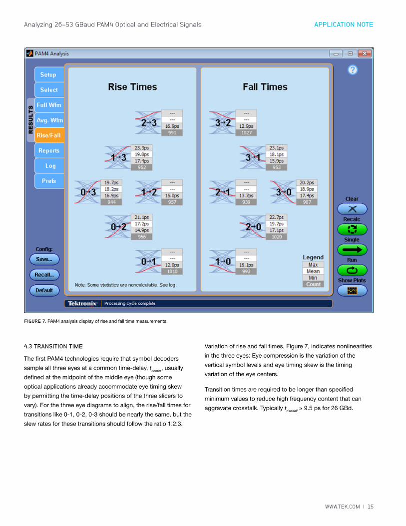
4.3 TRANSITION TIME
The first PAM4 technologies require that symbol decoders
sample all three eyes at a common time-delay, tcenter, usually
defined at the midpoint of the middle eye (though some
optical applications already accommodate eye timing skew
by permitting the time-delay positions of the three slicers to
vary). For the three eye diagrams to align, the rise/fall times for
transitions like 0-1, 0-2, 0-3 should be nearly the same, but the
slew rates for these transitions should follow the ratio 1:2:3.
Variation of rise and fall times, Figure 7, indicates nonlinearities
in the three eyes: Eye compression is the variation of the
vertical symbol levels and eye timing skew is the timing
variation of the eye centers.
Transition times are required to be longer than specified
minimum values to reduce high frequency content that can
aggravate crosstalk. Typically trise/fall ≥ 9.5 ps for 26 GBd.
FIGURE 7. PAM4 analysis display of rise and fall time measurements.
16 | WWW.TEK.COM
APPLICATION NOTEAnalyzing 26-53 GBaud PAM4 Optical and Electrical Signals
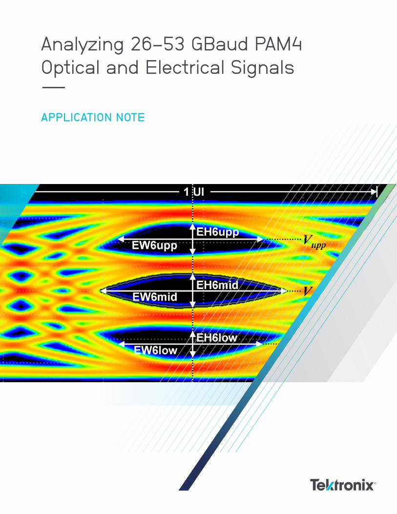
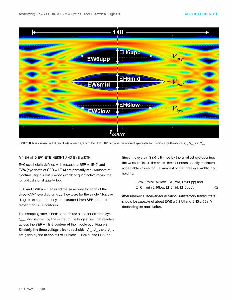
4.4 EH AND EW—EYE HEIGHT AND EYE WIDTH
EH6 (eye height defined with respect to SER = 1E-6) and
EW6 (eye width at SER = 1E-6) are primarily requirements of
electrical signals but provide excellent quantitative measures
for optical signal quality too.
EH6 and EW6 are measured the same way for each of the
three PAM4 eye diagrams as they were for the single NRZ eye
diagram except that they are extracted from SER-contours
rather than BER-contours.
The sampling time is defined to be the same for all three eyes,
tcenter, and is given by the center of the longest line that reaches
across the SER = 1E-6 contour of the middle eye, Figure 8.
Similarly, the three voltage slicer thresholds, Vlow, Vmid, and Vupp,
are given by the midpoints of EH6low, EH6mid, and EH6upp.
Since the system SER is limited by the smallest eye opening,
the weakest link in the chain, the standards specify minimum
acceptable values for the smallest of the three eye widths and
heights:
EW6 = min(EW6low, EW6mid, EW6upp) and
EH6 = min(EH6low, EH6mid, EH6upp). (5)
After reference receiver equalization, satisfactory transmitters
should be capable of about EW6 ≥ 0.2 UI and EH6 ≥ 30 mV
depending on application.
FIGURE 8. Measurement of EH6 and EW6 for each eye from the BER = 10-6 contours, definition of eye center and nominal slice thresholds, Vlow, Vmid, and Vupp.
WWW.TEK.COM | 17
APPLICATION NOTEAnalyzing 26-53 GBaud PAM4 Optical and Electrical Signals
4.5 SNDR—SIGNAL TO NOISE AND DISTORTION RATIO
Signal-to-noise-and-distortion ratio (SNDR) is a signal quality
figure of merit that compares electrical signal strength to the
combination of random noise and harmonic distortion.
Since SNDR is an automated oscilloscope measurement we
give a complete conceptual description in this section so that
you’ll understand what you’re measuring and how it should be
interpreted. The algorithmic details are in the standard.
SNDR is measured at the transmitter output and accounts for
transmitter noise and distortion but is independent of insertion
loss and ISI (inter-symbol interference). Unlike TDECQ, SNDR
does not account for the noise floor of the oscilloscope.
We derive SNDR from a linear fit to the measured waveform.
The fit is performed on a waveform acquisition of at least
one PRBS13Q repetition. Let the measured waveform be
y(k), where k runs from 1 to the product of the number of
samples per symbol and the length of the test pattern. The
pulse response, p(k), is extracted from the combination of
the measured waveform and the ideal symbol levels of the
PRBS13Q pattern. The pulse response is then used
to derive a linear fit to the waveform, f(k). The signal
strength is the maximum value of the pulse response,
pmax = max{p(k); for all k}.
The sample-by-sample fit error is e(k) = f(k) – y(k), the deviation
of the fit and the measurement. The distortion, se, is given by
the root mean square of the fit error, e(k):
The signal noise is measured at each of the four symbol levels
on low slope runs of at least six consecutive PAM4 signals. The
average of the four measurements gives sn.
SNDR is given by
(6)
In most cases SNDR must be larger than 31 dB.
18 | WWW.TEK.COM
APPLICATION NOTEAnalyzing 26-53 GBaud PAM4 Optical and Electrical Signals
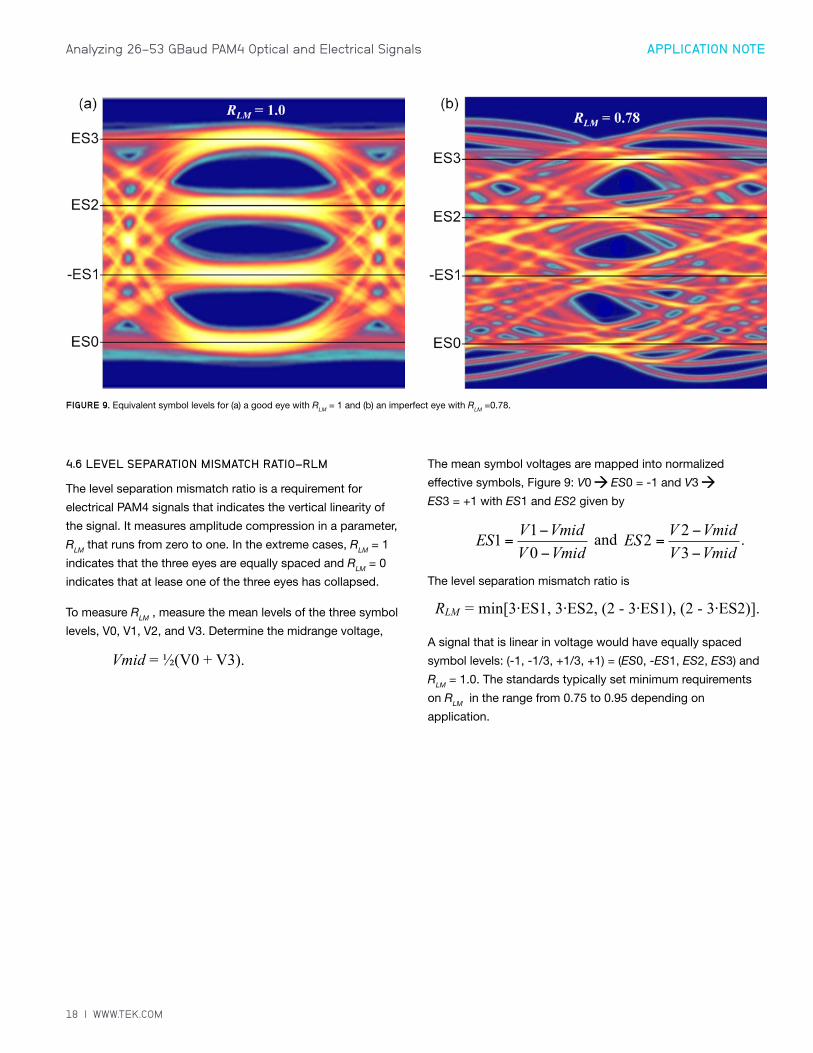
4.6 LEVEL SEPARATION MISMATCH RATIO—RLM
The level separation mismatch ratio is a requirement for
electrical PAM4 signals that indicates the vertical linearity of
the signal. It measures amplitude compression in a parameter,
RLM that runs from zero to one. In the extreme cases, RLM = 1
indicates that the three eyes are equally spaced and RLM = 0
indicates that at lease one of the three eyes has collapsed.
To measure RLM , measure the mean levels of the three symbol
levels, V0, V1, V2, and V3. Determine the midrange voltage,
The mean symbol voltages are mapped into normalized
effective symbols, Figure 9: V0 ES0 = -1 and V3
ES3 = +1 with ES1 and ES2 given by
The level separation mismatch ratio is
A signal that is linear in voltage would have equally spaced
symbol levels: (-1, -1/3, +1/3, +1) = (ES0, -ES1, ES2, ES3) and
RLM = 1.0. The standards typically set minimum requirements
on RLM in the range from 0.75 to 0.95 depending on
application.
FIGURE 9. Equivalent symbol levels for (a) a good eye with RLM = 1 and (b) an imperfect eye with RLM =0.78.
WWW.TEK.COM | 19
APPLICATION NOTEAnalyzing 26-53 GBaud PAM4 Optical and Electrical Signals
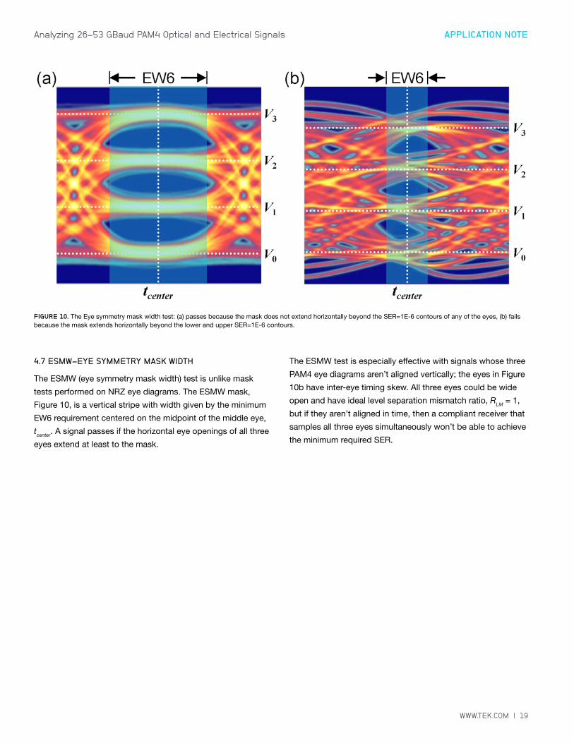
4.7 ESMW—EYE SYMMETRY MASK WIDTH
The ESMW (eye symmetry mask width) test is unlike mask
tests performed on NRZ eye diagrams. The ESMW mask,
Figure 10, is a vertical stripe with width given by the minimum
EW6 requirement centered on the midpoint of the middle eye,
tcenter. A signal passes if the horizontal eye openings of all three
eyes extend at least to the mask.
The ESMW test is especially effective with signals whose three
PAM4 eye diagrams aren’t aligned vertically; the eyes in Figure
10b have inter-eye timing skew. All three eyes could be wide
open and have ideal level separation mismatch ratio, RLM = 1,
but if they aren’t aligned in time, then a compliant receiver that
samples all three eyes simultaneously won’t be able to achieve
the minimum required SER.
FIGURE 10. The Eye symmetry mask width test: (a) passes because the mask does not extend horizontally beyond the SER=1E-6 contours of any of the eyes, (b) fails because the mask extends horizontally beyond the lower and upper SER=1E-6 contours.
20 | WWW.TEK.COM
APPLICATION NOTEAnalyzing 26-53 GBaud PAM4 Optical and Electrical Signals
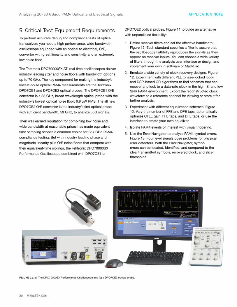
5. Critical Test Equipment Requirements To perform accurate debug and compliance tests of optical
transceivers you need a high performance, wide bandwidth
oscilloscope equipped with an optical to electrical, O/E,
convertor with great linearity and sensitivity and an extremely
low noise floor.
The Tektronix DPO70000SX ATI real time oscilloscopes deliver
industry leading jitter and noise floors with bandwidth options
up to 70 GHz. The key component for making the industry’s
lowest-noise optical PAM4 measurements are the Tektronix
DPO7OE1 and DPO7OE2 optical probes. The DPO7OE1 O/E
convertor is a 33 GHz, broad wavelength optical probe with the
industry’s lowest optical noise floor: 6.9 µW RMS. The all new
DPO7OE2 O/E convertor is the industry’s first optical probe
with sufficient bandwidth, 59 GHz, to analyze 53G signals.
Their well earned reputation for combining low noise and
wide bandwidth at reasonable prices has made equivalent
time sampling scopes a common choice for 28+ GBd PAM4
compliance testing. But with industry leading phase and
magnitude linearity plus O/E noise floors that compete with
their equivalent-time siblings, the Tektronix DPO70000SX
Performance Oscilloscope combined with DPO7OE1 or
DPO7OE2 optical probes, Figure 11, provide an alternative
with unparalleled flexibility:
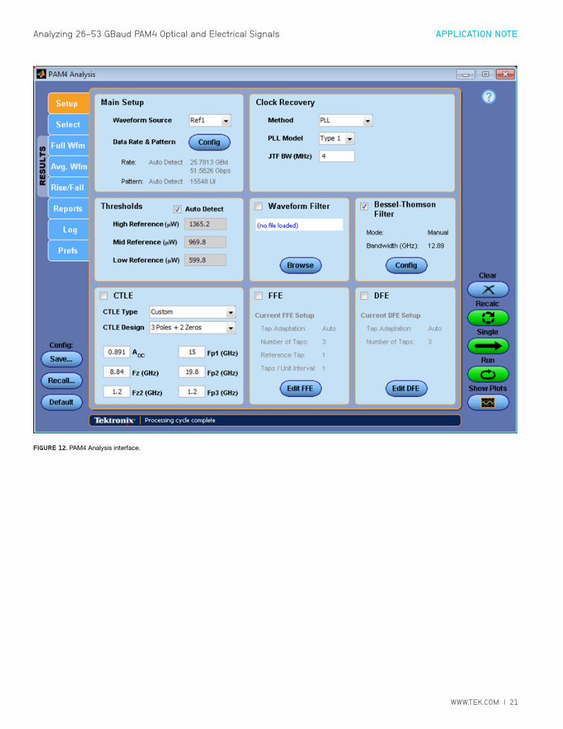
1. Define receiver filters and set the effective bandwidth, Figure 12. Each standard specifies a filter to assure that the oscilloscope faithfully reproduces the signals as they appear on receiver inputs. You can choose a wide variety of filters through the analysis user interface or design and implement your own in software or MathCad.
2. Emulate a wide variety of clock recovery designs, Figure 12. Experiment with different PLL (phase-locked loop) and DSP-based CR algorithms to find schemes that can recover and lock to a data-rate clock in the high ISI and low SNR PAM4 environment. Export the reconstructed clock waveform to a reference channel for viewing or store it for further analysis.
3. Experiment with different equalization schemes, Figure 12. Vary the number of FFE and DFE taps, automatically optimize CTLE gain, FFE taps, and DFE taps, or use the interface to create your own equalizer.
4. Isolate PAM4 events of interest with visual triggering.
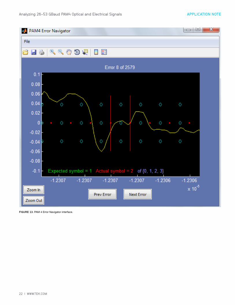
5. Use the Error Navigator to analyze PAM4 symbol errors, Figure 13. Four level signals pose problems for physical error detectors. With the Error Navigator, symbol errors can be located, identified, and compared to the ideal transmitted symbols, recovered clock, and slicer thresholds.
FIGURE 11. (a) The DPO70000SX Performance Oscilloscope and (b) a DPO7OE2 optical probe.
WWW.TEK.COM | 21
APPLICATION NOTEAnalyzing 26-53 GBaud PAM4 Optical and Electrical Signals
FIGURE 12. PAM4 Analysis interface.
22 | WWW.TEK.COM
APPLICATION NOTEAnalyzing 26-53 GBaud PAM4 Optical and Electrical Signals
FIGURE 13. PAM 4 Error Navigator interface.
WWW.TEK.COM | 23
APPLICATION NOTEAnalyzing 26-53 GBaud PAM4 Optical and Electrical Signals
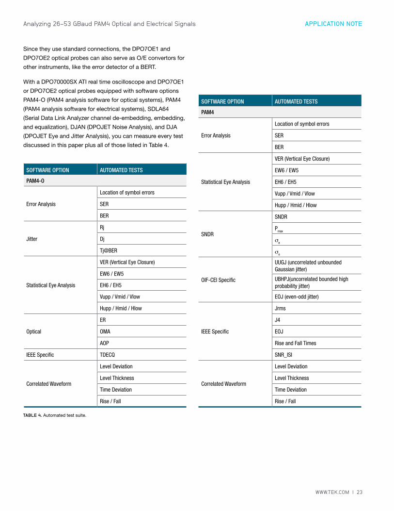
Since they use standard connections, the DPO7OE1 and
DPO7OE2 optical probes can also serve as O/E convertors for
other instruments, like the error detector of a BERT.
With a DPO70000SX ATI real time oscilloscope and DPO7OE1
or DPO7OE2 optical probes equipped with software options
PAM4-O (PAM4 analysis software for optical systems), PAM4
(PAM4 analysis software for electrical systems), SDLA64
(Serial Data Link Analyzer channel de-embedding, embedding,
and equalization), DJAN (DPOJET Noise Analysis), and DJA
(DPOJET Eye and Jitter Analysis), you can measure every test
discussed in this paper plus all of those listed in Table 4.
SOFTWARE OPTION AUTOMATED TESTS
PAM4-O
Error Analysis
Location of symbol errors
SER
BER
Jitter
Rj
Dj
Tj@BER
Statistical Eye Analysis
VER (Vertical Eye Closure)
EW6 / EW5
EH6 / EH5
V upp / V mid / V low
H upp / H mid / H low
Optical
ER
OMA
AOP
IEEE Specific TDECQ
Correlated Waveform
Level Deviation
Level Thickness
Time Deviation
Rise / Fall
SOFTWARE OPTION AUTOMATED TESTS
PAM4
Error Analysis
Location of symbol errors
SER
BER
Statistical Eye Analysis
VER (Vertical Eye Closure)
EW6 / EW5
EH6 / EH5
V upp / V mid / V low
H upp / H mid / H low
SNDR
SNDR
Pmax
se
sn
OIF-CEI Specific
UUGJ (uncorrelated unbounded Gaussian jitter)
UBHPJ(uncorrelated bounded high probability jitter)
EOJ (even-odd jitter)
IEEE Specific
Jrms
J4
EOJ
Rise and Fall Times
SNR_ISI
Correlated Waveform
Level Deviation
Level Thickness
Time Deviation
Rise / Fall
TABLE 4. Automated test suite.
Contact Information:
Australia* 1 800 709 465
Austria 00800 2255 4835
Balkans, Israel, South Africa and other ISE Countries +41 52 675 3777
Belgium* 00800 2255 4835
Brazil +55 (11) 3759 7627
Canada 1 800 833 9200
Central East Europe / Baltics +41 52 675 3777
Central Europe / Greece +41 52 675 3777
Denmark +45 80 88 1401
Finland +41 52 675 3777
France* 00800 2255 4835
Germany* 00800 2255 4835
Hong Kong 400 820 5835
India 000 800 650 1835
Indonesia 007 803 601 5249
Italy 00800 2255 4835
Japan 81 (3) 6714 3086
Luxembourg +41 52 675 3777
Malaysia 1 800 22 55835
Mexico, Central/South America and Caribbean 52 (55) 56 04 50 90
Middle East, Asia, and North Africa +41 52 675 3777
The Netherlands* 00800 2255 4835
New Zealand 0800 800 238
Norway 800 16098
People’s Republic of China 400 820 5835
Philippines 1 800 1601 0077
Poland +41 52 675 3777
Portugal 80 08 12370
Republic of Korea +82 2 6917 5000
Russia / CIS +7 (495) 6647564
Singapore 800 6011 473
South Africa +41 52 675 3777
Spain* 00800 2255 4835
Sweden* 00800 2255 4835
Switzerland* 00800 2255 4835
Taiwan 886 (2) 2656 6688
Thailand 1 800 011 931
United Kingdom / Ireland* 00800 2255 4835
USA 1 800 833 9200
Vietnam 12060128
* European toll-free number. If not accessible, call: +41 52 675 3777
Rev. 090617
Find more valuable resources at TEK.COM
Copyright © Tektronix. All rights reserved. Tektronix products are coverwed by U.S. and foreign patents, issued and pending. Information in this publication supersedes that in all previously published material. Specification and price change privileges reserved. TEKTRONIX and TEK are registered trademarks of Tektronix, Inc. All other trade names referenced are the service marks, trademarks or registered trademarks of their respective companies.
06/18 EA 51W-61416-0