Embed Size (px)
Citation preview
CSE 372 (Martin): FPGAs 1
CSE372Digital Systems Organization and Design
Lab
Prof. Milo Martin
Unit 2: Field Programmable Gate Arrays (FPGAs)
CSE 372 (Martin): FPGAs 2
Announcements
• Lab 1 due in one week
• Questions/comments?
• Testbench coming soon (according to the TAs)
• Today’s lecture:
• How FPGAs work
CSE 372 (Martin): FPGAs 3
Field Programmable Gate Array (FPGA)
• An alternative to a “custom” design• A high-end custom design “mask set” is expensive (millions of $!)
• Advantages• Simplicity of gate-level design (no transistor-level design)
• Fast time-to-market
• No manufacturing delay
• Can fix design errors over time (more like software)
• Disadvantages• Expensive: unit cost is higher
• Inefficient: slower and more power hungry
• Result: good for low-volume or initial designs
CSE 372 (Martin): FPGAs 4
Early Programmable Logic Device…
From UC-Berkeley CS152 slides
CSE 372 (Martin): FPGAs 5
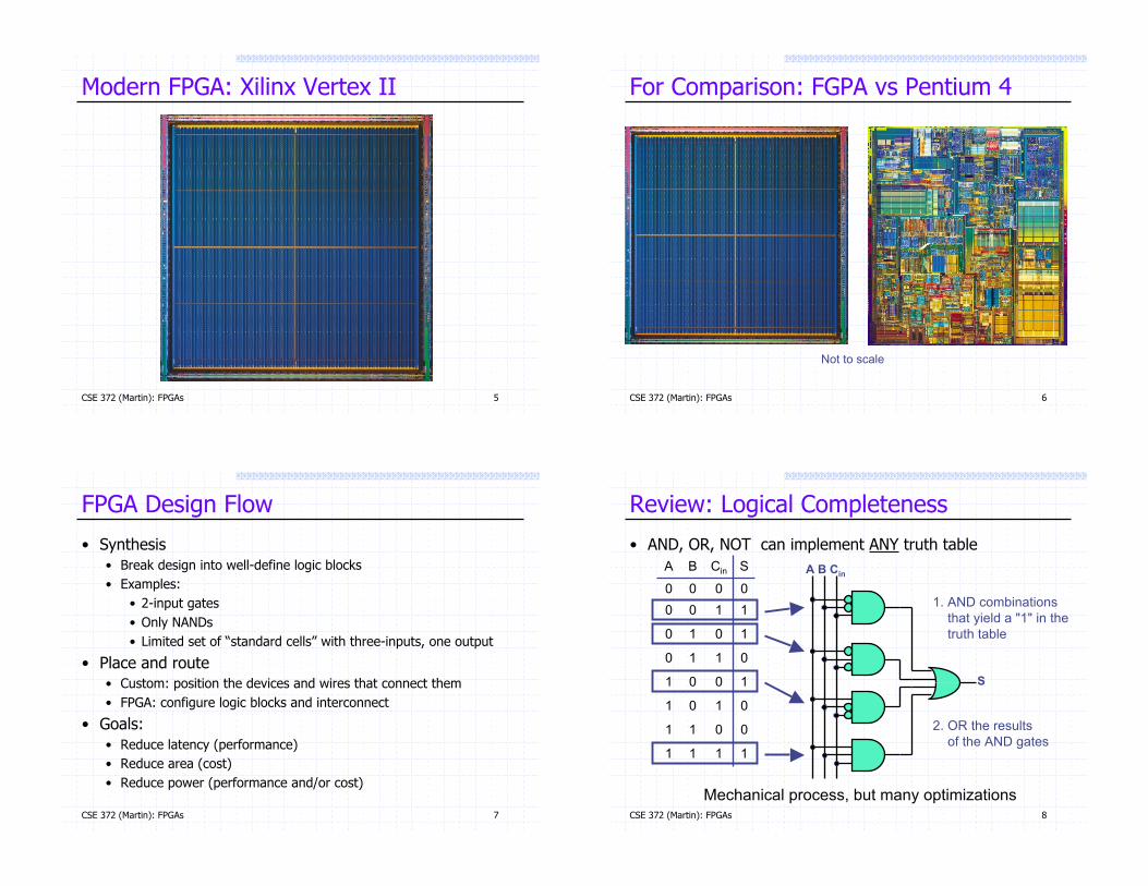
Modern FPGA: Xilinx Vertex II
CSE 372 (Martin): FPGAs 6
For Comparison: FGPA vs Pentium 4
Not to scale
CSE 372 (Martin): FPGAs 7
FPGA Design Flow
• Synthesis
• Break design into well-define logic blocks
• Examples:
• 2-input gates
• Only NANDs
• Limited set of “standard cells” with three-inputs, one output
• Place and route
• Custom: position the devices and wires that connect them
• FPGA: configure logic blocks and interconnect
• Goals:
• Reduce latency (performance)
• Reduce area (cost)
• Reduce power (performance and/or cost)
CSE 372 (Martin): FPGAs 8
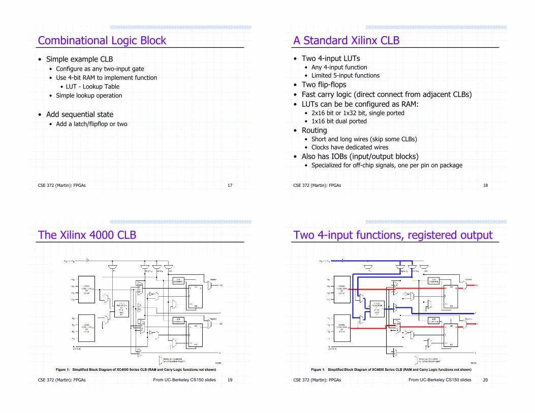
Review: Logical Completeness
• AND, OR, NOT can implement ANY truth table
1010
1001
0101
0011
1
0
0
0
A
110
011
1
0
B
11
00
SCin A B Cin
S
1. AND combinations
that yield a "1" in the
truth table
2. OR the results
of the AND gates
Mechanical process, but many optimizations

CSE 372 (Martin): FPGAs 9
Our Old Friend, The Full Adder
• Add two bits and carry-inproduce one-bit sum and carry-out
0
1
0
0
1
1
1
0
1
0
1
1
0
0
1
0
110
001
101
011
S
1
1
0
0
B
10
00
1
0
A
1
0
CoutCin
Add Sn
An
1 1
CarryInn
CarryOutn
Bn
1
CSE 372 (Martin): FPGAs 10
A Better Full Adder
!module full_adder(s, cout, a, b, cin); output s, cout; input a, b, cin;
xor (t1, a, b); xor (s, t1, cin); and (t2, t1, cin); and (t3, a, b); or (cout, t2, t3);endmodule
Add Sn
An
1 1
CarryInn
CarryOutn
Bn
1
sab
cin
t1
t3
cout
t2
CSE 372 (Martin): FPGAs 11
A Simple (Fake) FPGA Substrate
CSE 372 (Martin): FPGAs 12
How Do We “Route” Signals?
• Switch matrix
• Each junction has 6 “switches”
• Each switch is a pass gate
• Programming
• Each pass gate controlled by 1-bit flip-flop
• 0/1 value of flip-flop set at configuration
• Programmable “interconnect”
• Allows for arbitrary routing of signals
• Each segment adds delay
• Takes up lots of chip area
Pass Gate
Switch

CSE 372 (Martin): FPGAs 13
On-Chip Wires
©IB
M
CSE 372 (Martin): FPGAs 14
More Wires
IBM CMOS7, 6 layers of copper wiring
©IB
M
CSE 372 (Martin): FPGAs 15
Configure This As a Full Adder
s
a
b
cin
cout
CSE 372 (Martin): FPGAs 16
CLB
CLBCLB CLB
CLB CLB
A Better FPGA
• Replace gates with general “CLB”
• Combinational logic block
CSE 372 (Martin): FPGAs 17
Combinational Logic Block
• Simple example CLB
• Configure as any two-input gate
• Use 4-bit RAM to implement function
• LUT - Lookup Table
• Simple lookup operation
• Add sequential state
• Add a latch/flipflop or two
CSE 372 (Martin): FPGAs 18
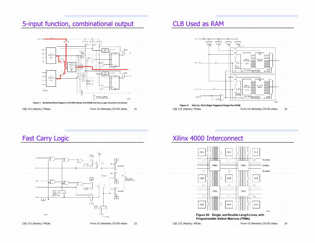
A Standard Xilinx CLB
• Two 4-input LUTs• Any 4-input function
• Limited 5-input functions
• Two flip-flops
• Fast carry logic (direct connect from adjacent CLBs)
• LUTs can be be configured as RAM:• 2x16 bit or 1x32 bit, single ported
• 1x16 bit dual ported
• Routing• Short and long wires (skip some CLBs)
• Clocks have dedicated wires
• Also has IOBs (input/output blocks)• Specialized for off-chip signals, one per pin on package
CSE 372 (Martin): FPGAs 19
The Xilinx 4000 CLB
From UC-Berkeley CS150 slides CSE 372 (Martin): FPGAs 20
Two 4-input functions, registered output
From UC-Berkeley CS150 slides
CSE 372 (Martin): FPGAs 21
5-input function, combinational output
From UC-Berkeley CS150 slides CSE 372 (Martin): FPGAs 22
CLB Used as RAM
From UC-Berkeley CS150 slides
CSE 372 (Martin): FPGAs 23
Fast Carry Logic
From UC-Berkeley CS150 slides CSE 372 (Martin): FPGAs 24
Xilinx 4000 Interconnect
From UC-Berkeley CS150 slides
CSE 372 (Martin): FPGAs 25
Switch Matrix
From UC-Berkeley CS150 slides CSE 372 (Martin): FPGAs 26
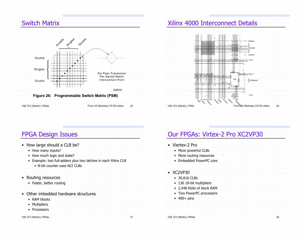
Xilinx 4000 Interconnect Details
From UC-Berkeley CS150 slides
CSE 372 (Martin): FPGAs 27
FPGA Design Issues
• How large should a CLB be?
• How many inputs?
• How much logic and state?
• Example: two full-adders plus two latches in each Xilinx CLB
• N-bit counter uses N/2 CLBs
• Routing resources
• Faster, better routing
• Other imbedded hardware structures
• RAM blocks
• Multipliers
• Processors
CSE 372 (Martin): FPGAs 28
Our FPGAs: Virtex-2 Pro XC2VP30
• Viertex-2 Pro
• More powerful CLBs
• More routing resources
• Embedded PowerPC core
• XC2VP30
• 30,816 CLBs
• 136 18-bit multipliers
• 2,448 Kbits of block RAM
• Two PowerPC processors
• 400+ pins
CSE 372 (Martin): FPGAs 29
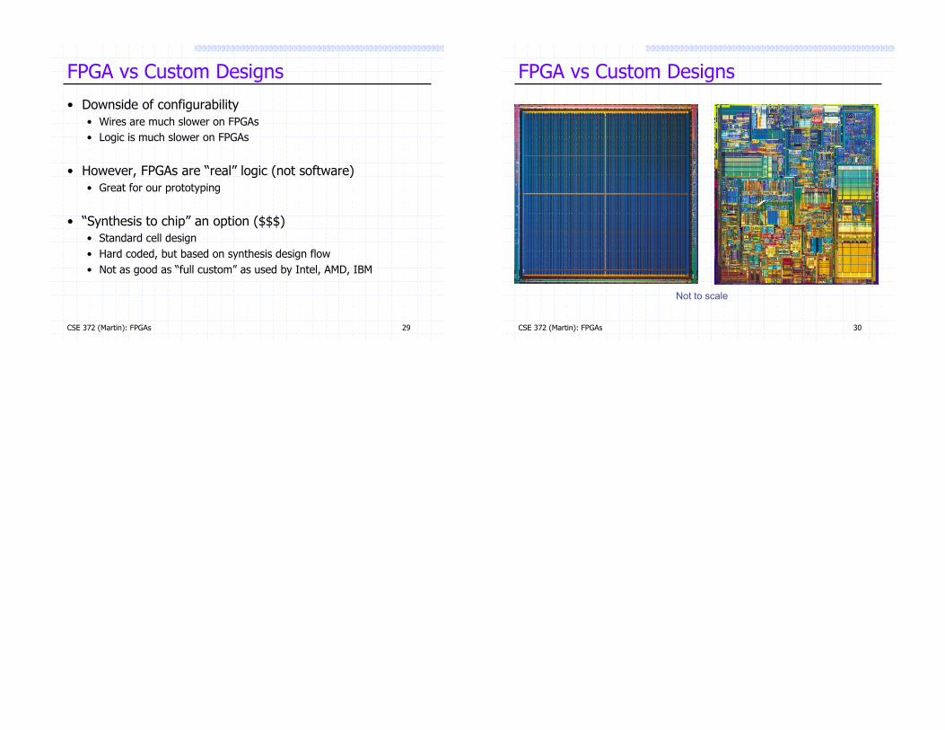
FPGA vs Custom Designs
• Downside of configurability
• Wires are much slower on FPGAs
• Logic is much slower on FPGAs
• However, FPGAs are “real” logic (not software)
• Great for our prototyping
• “Synthesis to chip” an option ($$$)
• Standard cell design
• Hard coded, but based on synthesis design flow
• Not as good as “full custom” as used by Intel, AMD, IBM
CSE 372 (Martin): FPGAs 30
FPGA vs Custom Designs
Not to scale
![Architecture of field-programmable gate arrays ...arantxa.ii.uam.es/~die/[Lectura FPGA Architecture] Architecture of... · Architecture of Field-Programmable Gate Arrays JONATHAN](https://img.pdfslide.net/doc/110x75/5f41b9382d13750b786f03bd/architecture-of-field-programmable-gate-arrays-dielectura-fpga-architecture.jpg)