Embed Size (px)
Citation preview
JOURNAL OF SEMICONDUCTOR TECHNOLOGY AND SCIENCE, VOL.13, NO.4, AUGUST, 2013 http://dx.doi.org/10.5573/JSTS.2013.13.4.291
Manuscript received Dec. 30, 2012; accepted Mar. 9, 2013
Hyuk-Jun Lee is a corresponding author and with Sogang University
E-mail : [email protected]
Application-aware Design Parameter Exploration
of NAND Flash Memory
Kwanhu Bang, Dong-Gun Kim, Sang-Hoon Park, Eui-Young Chung, and Hyuk-Jun Lee
Abstract—NAND flash memory (NFM) based storage
devices, e.g. Solid State Drive (SSD), are rapidly
replacing conventional storage devices, e.g. Hard Disk
Drive (HDD). As NAND flash memory technology
advances, its specification has evolved to support
denser cells and larger pages and blocks. However,
efforts to fully understand their impacts on design
objectives such as performance, power, and cost for
various applications are often neglected. Our research
shows this recent trend can adversely affect the design
objectives depending on the characteristics of
applications. Past works mostly focused on improving
the specific design objectives of NFM based systems
via various architectural solutions when the
specification of NFM is given. Several other works
attempted to model and characterize NFM but did
not access the system-level impacts of individual
parameters. To the best of our knowledge, this paper
is the first work that considers the specification of
NFM as the design parameters of NAND flash storage
devices (NFSDs) and analyzes the characteristics of
various synthesized and real traces and their
interaction with design parameters. Our research
shows that optimizing design parameters depends
heavily on the characteristics of applications. The
main contribution of this research is to understand
the effects of low-level specifications of NFM, e.g. cell
type, page size, and block size, on system-level metrics
such as performance, cost, and power consumption in
various applications with different characteristics, e.g.
request length, update ratios, read-and-modify ratios.
Experimental results show that the optimized page
and block size can achieve up to 15 times better
performance than the conventional NFM configuration
in various applications. The results can be used to
optimize the system-level objectives of a system with
specific applications, e.g. embedded systems with
NFM chips, or predict the future direction of NFM.
Index Terms—NAND Flash Memory (NFM), NAND
Flash Storage Devices (NFSD), specifications, design
parameters
I. INTRODUCTION
Storage devices based on NAND flash memory (NFM),
e.g. solid-state disks (SSDs), are rapidly widening their
market share thanks to superior characteristics of NFM
such as faster access speed, stronger shock-resistance,
and lighter weight than conventional magnetic disks.
Besides SSDs, NAND flash-based storage devices
(NFSDs) are used in USB memory sticks,
portable/mobile devices, etc. As many manufacturers
continuously reduce the cost-per-bit gap between NFSDs
and conventional non-volatile storage devices, e.g. HDD,
NFM becomes dramatically denser and cheaper.
From a system perspective, however, NFSDs based on
denser NFM chips only reduce the cost but does not
necessarily improve the performance of system. This is
shown in Fig. 1. It shows the trend of two different
design objectives, performance and cost, as the NFM
technology advances. Released year, page size, number
of pages per block for several generation of NFM chips
are provided under the x-axis and they reflect the current
292 KWANHU BANG et al : APPLICATION-AWARE DESIGN PARAMETER EXPLORATION OF NAND FLASH MEMORY
technology trend, which increases the size of a page and
the number of pages within a block. The cost in the
figure is continuously decreasing as technology advances.
However, the performance represented by throughput,
shows two different trends with respect to the
applications running on the NFSD. This indicates that the
increased size of pages and blocks may be harmful under
certain applications.
This measurement clearly questions a conventional
wisdom that the cheaper and denser NFM thanks to
advance in technology is helpful to satisfy various design
objectives of NFSDs. In other words, as shown in Fig. 1,
the increased page and block sizes successfully reduce
cost-per-bit of NFSDs but their effects on the
performance are different from applications to
applications. For this reason, to really understand the
system-level impact of technology advance in NFM, we
need to analyze the design parameters, i.e. specification
of NFM, and the characteristics of applications and
understand how they affect the system-level objectives of
NFSDs.
Several previous works optimized the design
objectives, e.g. performance, of NFSDs by improving the
architecture of NFSD [1] or exploiting parallelism of
multiple NFM chips [7]. In [3-5], several system-level
solutions and reconfigurable FTL design such as
concurrency are considered in optimizing the design
objectives of NFSD. All these works, however, did not
pay attention to the impact of design parameters of NFM
such as page or block size or characteristics of
applications.
Past works in the area of characterizing and modeling
NFM are presented in [2] and [6]. They characterized
various commercial NFM products [2] and modeled
NFM's power consumption at the transistor level [6].
However, they did not analyze how the characteristics of
NFM affect system-level performance of NFSDs.
Compared to earlier works, our research considers
specification of NFM as design parameters of NFSDs
and studies their impacts on the system-level metrics.
Our contribution in this research can be itemized into
three parts.
• First, we identify essential design parameters of NFM,
e.g. cell type, page size, block size, which affect
various design objectives. In addition, we define and
extract crucial attributes from the traces of applications,
e.g. request length, update ratios, and read-and-modify
ratios, which characterize the applications.
• Second, we analyze the relationship between the
design objectives such as performance, cost, and
power and our new design parameters and trace
attributes. For instance, to determine an optimal page
and block size, we have to consider their interaction
with application attributes that affect the number of
write operations and read-and-modify operations,
erase time, and garbage collection time.
• Finally, via intensive simulations and analysis, we
show that optimizing the design parameters of NFM
heavily depends on the characteristics of applications
and significantly improves the performance, cost, and
power.
The remainder of this paper is organized as follows: In
Section II, background knowledge on the NFM
architecture, software layer, and analysis metrics such as
performance, cost, and power are presented. In Section
III, we define key parameters in NFM specification, e.g.
cell type, page size, and block size, which can be
optimized as NFSD's design parameters. In addition, to
characterize different applications, we define trace
parameters. Along with these definitions, we provide our
analysis on how each design or trace parameter interacts
with various design objectives. Finally, we show
experimental results for various applications including
synthesized and real traces in Section IV, followed by
conclusion in Section V.
0 . 50 . 5 50 . 60 . 6 50 . 70 . 7 50 . 80 . 8 50 . 90 . 9 51
00 . 20 . 40 . 60 . 811 . 21 . 41 . 61 . 82
( 2 0 0 8 , 4 K B , 1 2 8 ) ( 2 0 1 0 , 8 K B , 2 5 6 ) ( p r e d i c t e d , 1 6 K B , 5 1 2 )N F M c o n f i g u r a t i o n ( y e a r , p a g e s i z e , # p a g e s / b l o c k ) N ormali zedE sti mat edC ost >per >bi t
N ormzli edTh rough put
C o s t R a n d o m S e q
Fig. 1. Throughput and cost of NFSDs using three generations
of NFM chips for two different applications.
JOURNAL OF SEMICONDUCTOR TECHNOLOGY AND SCIENCE, VOL.13, NO.4, AUGUST, 2013 293
II. PRELIMINARIE
1. NAND Flash Memory (NFM)
NAND flash memory is a nonvolatile memory and
stores data by pushing electrons into the floating gate of
each cell. Since the floating gate can isolate the electrons,
the NFM can maintain their data without power supply.
Furthermore, the NFM is one of the densest memories
and much more reliable than magnetic disks. It is used as
a main storage medium of many storage devices.
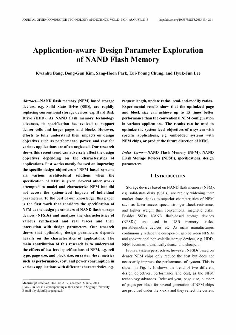
The internal architecture of NFM is shown in Fig. 2.
The NFM architecture consists of a cell array for storing
data, a page buffer that temporarily buffers data before
the data is written or after it is read, command logic
circuits to control the NFM, and other peripherals for
various purposes.
To achieve the high density, NFM does not allow
random access to cells in the array. All data accesses are
executed through the page buffer whose size is same as
the size of a page. For this reason, the minimum size of
accessed data by reads and writes is a page. A page
update happens when a write is requested to an already-
written page. Its request unit is a logical sector.
Operating system accesses storage devices using a
logical sector address (LSA) and the size of a sector is
512 bytes. To update or reuse a written page, the cells
belonging to the page are required to be erased in
advance. An erase operation is done in the unit of a block,
which is a group of pages. Other than these unique
characteristics, the architecture and behavior of other
peripherals, including command logic is very similar to
that of DRAM.
2. Flash Translation Layer (FTL)
A flash translation layer (FTL) is a software layer used
by many NFSDs to fill the gap between conventional file
systems and NFM based file systems. It serves multiple
roles such as address translation, garbage collection, and
wear-leveling, each of which is closely related with the
design objectives of NFSDs.
Most address translation schemes of FTL are based on
a mapping table between logical and physical addresses
and the granularity of the mapping table is one of the
most important factors for the overall performance of
NFSDs. Due to the limited size of volatile memories,
either caching the mapping table during execution of the
FTL or a hybrid-level FTL has been proposed, which
combines a cheap but limited-performance block mapping
method and a costly but good-performance page mapping
method [9]. In addition, there is a scheme that uses
volatile memories with NFM to build a hierarchy of map
table [10].
A garbage collection scheme is also a crucial factor for
the performance of NFSDs since it dictates the number of
valid page copy and erase operations of NFM. Most FTL
schemes have focused on implementing effective
garbage collection.
Wear-leveling is an algorithm developed to extend the
limited life-time. The life-time is determined by the
number of erase operations experienced by a block of the
NFM. A block guarantees its functionality until it
experiences a fixed number of erase operations. The total
number of erase operations decreases as the number of
bits stored within a cell increases.
3. Analysis Metrics
In this paper, three metrics are defined to evaluate the
effects of different design parameters. They are
performance, cost, and power. Performance is an
essential metric in evaluating NFSDs whereas
manufacturers have additionally focused on lowering the
cost of NFM. Recently due to the explosive growth of
mobile devices, power consumption is also seriously
considered. To define metrics mathematically, we list
parameters used in definition of metrics in Table 1.
C O M M A N DI N T E R F A C EL O G I CP R O G R A ME R A S EC O N T R O L L E RH V G E N E R A T I O N
C O M M A N DR E G I S T E RD A T AR E G I S T E R
1 6 3 8 4 M b i t + 5 1 2 M b i tN A N D F l a s hM E M O R Y A R R A YP A G E B U F F E RY D E C O D E RB U F F E R S
XD ECOD ER
I O
P R EA L EC L E/ W E/ C E/ W P/ R EA D D R E S SR E G I S T E R /C O U N T E RA 3 1 ~ A 0
Fig. 2. Internal architecture of NFM based on [12].
294 KWANHU BANG et al : APPLICATION-AWARE DESIGN PARAMETER EXPLORATION OF NAND FLASH MEMORY
(1) Performance: Generally, throughput is used as a
performance metric in NFSDs. Throughput is computed
from the amount of transferred data and its latency using
(1). Equations defined in [7] can be used if the multi-
channel/way architecture is used. A simulator we
develop receives traces as an input and produces a
sequence of NFM operations as an output. Received
traces contain read/write information, start addresses of
requests and request length in the unit of a sector. If the
page size is 2 KB or 4 KB, a page occupies 4 or 8 sectors
respectively. The latency of NFM operations are
described in NFM's datasheet [12]. Using this
information, we calculate the total latency of applications,
measure the amount of transferred data, and compute the
throughput as shown below
total amounts of transferred data
throughputtotal latency for executing data
= (1)
The performance of NFSD mostly depends on the
performance of write operations. Factors affecting the
performance of write operations are (1) the frequency of
write operations, (2) the frequency of read operations
due to read-and-modify operations and (3) the time for
erase and garbage collections. The performance of
garbage collection again depends on the frequency of
garbage collection and the number of valid page copies
before the erase. These factors will be further discussed
in the later sections.
(2) Cost: Cost can be expressed in terms of chip area.
In this paper, we use area to compare costs. A smaller
NFM area makes it possible to integrate more chips per
die and it makes NFM chips cheaper. Cost for
peripherals not directly related to the cell area such as
command logic or address counters can be considered
fixed. An important factor for the cost is the architecture
of the NFM array and peripherals connected the NFM
array directly. A larger page size requires a larger page
register. In addition, as its block size gets larger, logic for
the erase controller needs more area. We call these page
overhead and block overhead, respectively. Eq. (2)
expresses the cost in terms of bits per block.
{( / ) / }b p p b p bC S N O O Nτ= + + (2)
In this equation, page and block overhead represent
how much area is consumed by overheads in addition to
the page itself. In this equation, τ represents a cell type. If
a cell is a single-level cell (SLC), τ is 2. If a cell is a
multi-level cell (MLC), τ is 4. Thus, MLC has the lower
cost. Ob is a block overhead that ranges roughly from 2
to 5. Op is a page overhead that ranges roughly from 1 to
10. Ob and Op are proportional to the block and page size.
The number of blocks and the number of pages have
inverse relationship if the total capacity of two NFSDs
are same.
(3) Power: To calculate the total power consumption
by NFM, the power consumption for each operation is
separately calculated and the consumption for all
operations are summed at the end. A majority of
operations for NFM are read, program, and erase. By
using a simulator that we implement, how many times
each operation is executed can be logged. The power
consumption for each operation is shown below.
t CC TRANS TRANSP V I t= (3)
1 4( )r CC CC CC RP V I I t= − (4)
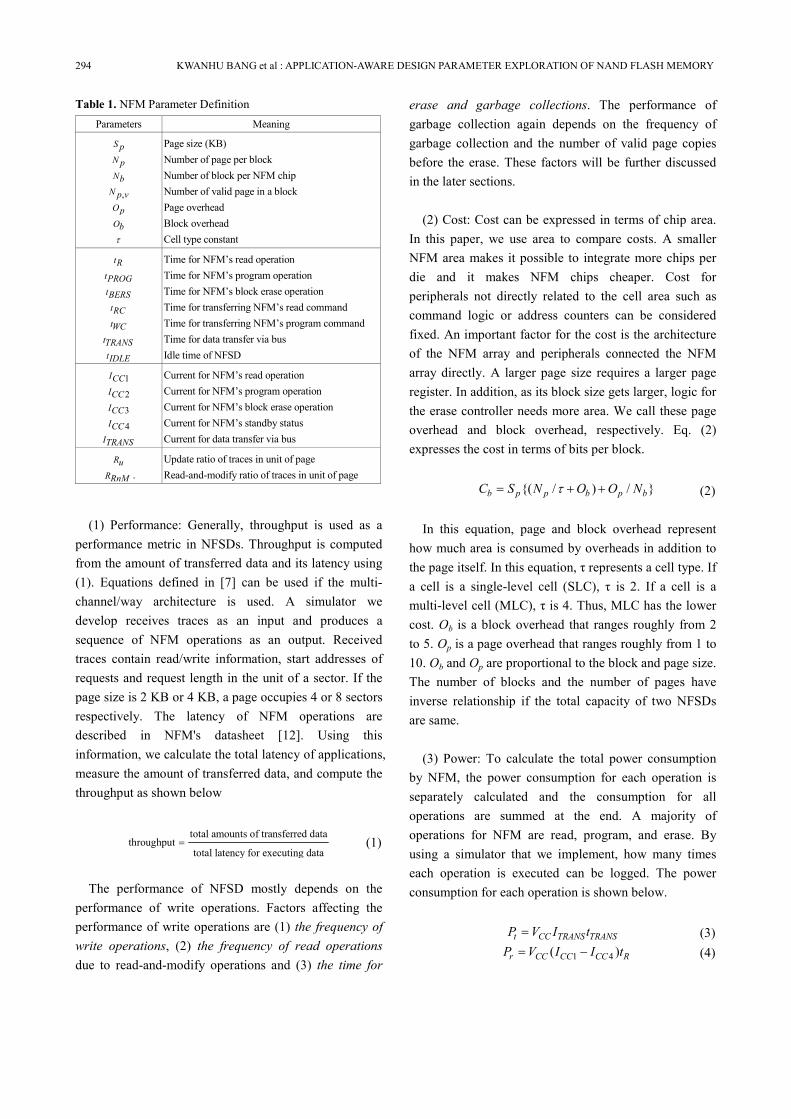
Table 1. NFM Parameter Definition
Parameters Meaning
S p
N p
Nb
,N p v
Op
Ob
τ
Page size (KB)
Number of page per block
Number of block per NFM chip
Number of valid page in a block
Page overhead
Block overhead
Cell type constant
tR
tPROG
tBERS
tRC
tWC
tTRANS
tIDLE
Time for NFM’s read operation
Time for NFM’s program operation
Time for NFM’s block erase operation
Time for transferring NFM’s read command
Time for transferring NFM’s program command
Time for data transfer via bus
Idle time of NFSD
1ICC
2ICC
3ICC
4ICC
ITRANS
Current for NFM’s read operation
Current for NFM’s program operation
Current for NFM’s block erase operation
Current for NFM’s standby status
Current for data transfer via bus
Ru
RRnM .
Update ratio of traces in unit of page
Read-and-modify ratio of traces in unit of page
JOURNAL OF SEMICONDUCTOR TECHNOLOGY AND SCIENCE, VOL.13, NO.4, AUGUST, 2013 295
2 4( )p CC CC CC PROGP V I I t= − (5)
R r tP P P= + (6)
P p tP P P= + (7)
3 4( )E CC CC CC BERSP V I I t= − (8)
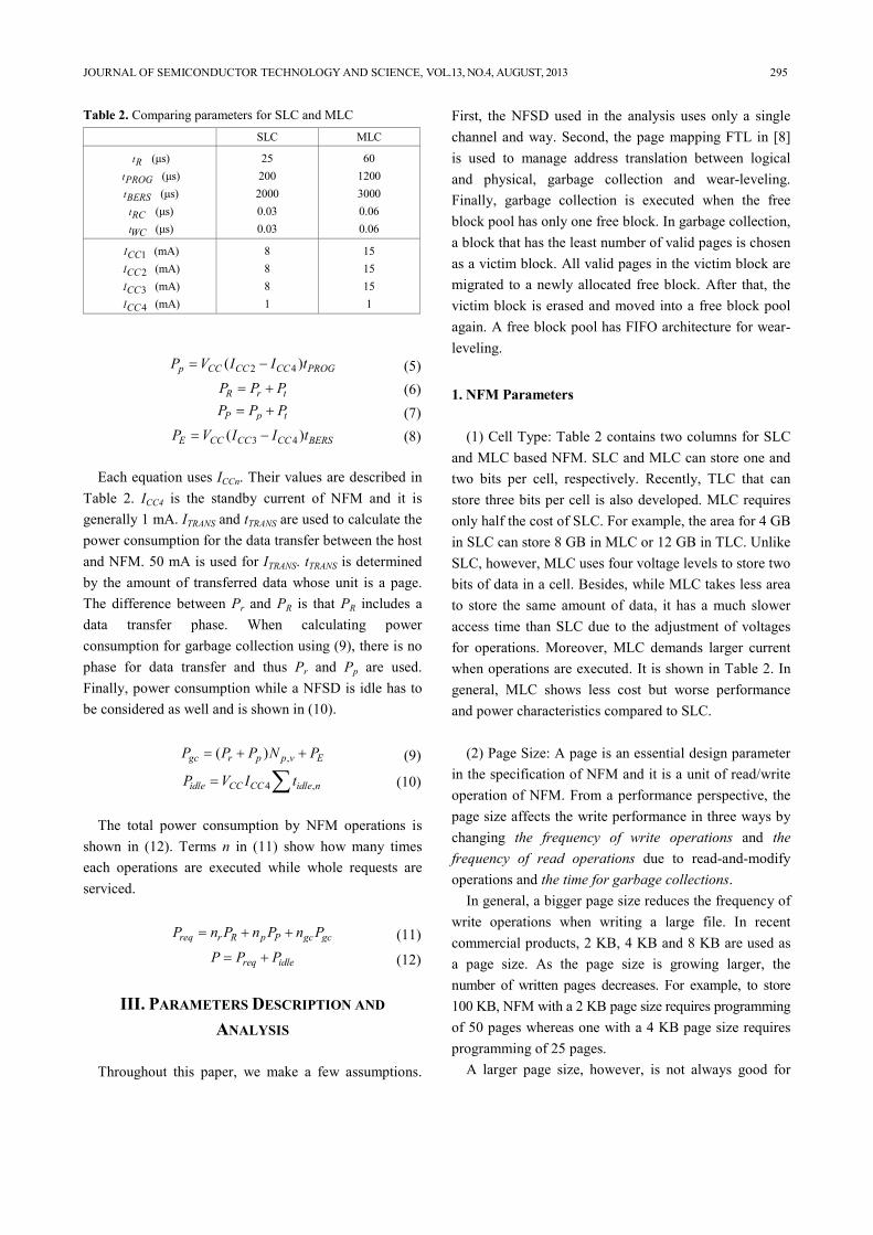
Each equation uses ICCn. Their values are described in
Table 2. ICC4 is the standby current of NFM and it is
generally 1 mA. ITRANS and tTRANS are used to calculate the
power consumption for the data transfer between the host
and NFM. 50 mA is used for ITRANS. tTRANS is determined
by the amount of transferred data whose unit is a page.
The difference between Pr and PR is that PR includes a
data transfer phase. When calculating power
consumption for garbage collection using (9), there is no
phase for data transfer and thus Pr and Pp are used.
Finally, power consumption while a NFSD is idle has to
be considered as well and is shown in (10).
,( )gc r p p v EP P P N P= + + (9)
4 ,idle CC CC idle nP V I t= ∑ (10)
The total power consumption by NFM operations is
shown in (12). Terms n in (11) show how many times
each operations are executed while whole requests are
serviced.
req r R p P gc gcP n P n P n P= + + (11)
req idleP P P= + (12)
III. PARAMETERS DESCRIPTION AND
ANALYSIS
Throughout this paper, we make a few assumptions.
First, the NFSD used in the analysis uses only a single
channel and way. Second, the page mapping FTL in [8]
is used to manage address translation between logical
and physical, garbage collection and wear-leveling.
Finally, garbage collection is executed when the free
block pool has only one free block. In garbage collection,
a block that has the least number of valid pages is chosen
as a victim block. All valid pages in the victim block are
migrated to a newly allocated free block. After that, the
victim block is erased and moved into a free block pool
again. A free block pool has FIFO architecture for wear-
leveling.
1. NFM Parameters
(1) Cell Type: Table 2 contains two columns for SLC
and MLC based NFM. SLC and MLC can store one and
two bits per cell, respectively. Recently, TLC that can
store three bits per cell is also developed. MLC requires
only half the cost of SLC. For example, the area for 4 GB
in SLC can store 8 GB in MLC or 12 GB in TLC. Unlike
SLC, however, MLC uses four voltage levels to store two
bits of data in a cell. Besides, while MLC takes less area
to store the same amount of data, it has a much slower
access time than SLC due to the adjustment of voltages
for operations. Moreover, MLC demands larger current
when operations are executed. It is shown in Table 2. In
general, MLC shows less cost but worse performance
and power characteristics compared to SLC.
(2) Page Size: A page is an essential design parameter
in the specification of NFM and it is a unit of read/write
operation of NFM. From a performance perspective, the
page size affects the write performance in three ways by
changing the frequency of write operations and the
frequency of read operations due to read-and-modify
operations and the time for garbage collections.
In general, a bigger page size reduces the frequency of
write operations when writing a large file. In recent
commercial products, 2 KB, 4 KB and 8 KB are used as
a page size. As the page size is growing larger, the
number of written pages decreases. For example, to store
100 KB, NFM with a 2 KB page size requires programming
of 50 pages whereas one with a 4 KB page size requires
programming of 25 pages.
A larger page size, however, is not always good for
Table 2. Comparing parameters for SLC and MLC
SLC MLC
tR (µs)
tPROG (µs)
tBERS (µs)
tRC (µs)
tWC (µs)
25
200
2000
0.03
0.03
60
1200
3000
0.06
0.06
1ICC (mA)
2ICC (mA)
3ICC (mA)
4ICC (mA)
8
8
8
1
15
15
15
1
296 KWANHU BANG et al : APPLICATION-AWARE DESIGN PARAMETER EXPLORATION OF NAND FLASH MEMORY
several reasons. First, a read-and-modify problem is
introduced when only a part of page is modified. It
happens frequently when the write request is not aligned
to a page boundary. This problem can be categorized into
two cases. The first case is when a request length is
stretched over two pages because the start address of the
request is not aligned to the page boundary. The second
case is when a request length is smaller than the page
size and cannot fill the whole page. In this case, older
contents in the page that are not changed by the new
request have to be preserved. In both cases, not all data in
the page are modified. Thus, a NFM controller transfers
data to a page register and modifies a part of data. Then
the modified data in the register is sent back to NFM
again. This procedure requires an extra read operation
and adds tR to tPROG. This increases the frequency of read
operations upon writes and degrades performance. In
case when a request is aligned to the page, on the other
hand, it needs only a write operation and the whole page
is written with data of the new request .
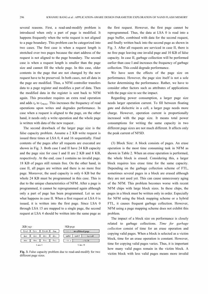
The second drawback of the larger page size is the
false capacity problem. Assume a 2 KB write request is
issued three times at LSA 0, 4 and 16 sequentially. Final
contents of the pages after all requests are executed are
shown in Fig. 3. Both case I and II have 24 KB capacity
and the page size for case I and II are 2 KB and 8 KB,
respectively. At the end, case I contains no invalid page.
18 KB of pages still remain free. On the other hand, in
case II, all pages are written and there is no more free
page. Moreover, the used capacity is only 6 KB but the
whole 24 KB must be programmed in this case. This is
due to the unique characteristics of NFM. After a page is
programmed, it cannot be reprogrammed again although
only a part of page has been programmed. Let us see
what happens in case II. When a first request at LSA 0 is
issued, it is written into the first page. Since LSA 0
through LSA 15 are mapped to a single page, the second
request at LSA 4 should be written into the same page as
the first request. However, the first page cannot be
reprogrammed. Thus, the data at LSA 0 is read into a
page buffer, combined with data for the second request,
and finally written back into the second page as shown in
Fig. 3. After all requests are serviced in case II, there is
no free page leaving one invalid page and 10 KB of false
capacity. In case II, garbage collection will be performed
earlier than case I and increases the frequency of garbage
collection. This could degrade performance.
We have seen the effects of the page size on
performance. However, the page size itself is not a sole
factor determining the performance. Rather, we have to
consider other factors such as attributes of applications
with the page size to see the impact.
Regarding power consumption, a larger page size
needs larger operation current. To fill between floating
gate and dielectric in a cell, a larger page needs more
charge. However, operation current is proportionally
increased with the page size. It means total power
consumptions for writing the same capacity in two
different page sizes are not much different. It affects only
the peak current of NFSD.
(3) Block Size: A block consists of pages. An erase
operation is the most time consuming task in NFM as
shown in Table 2. When an erase operation is performed,
the whole block is erased. Considering this, a larger
block requires less erase time for the same capacity.
Depending on the garbage collection scheme of FTL,
sometimes several pages in a block are erased although
they are not used yet. This can cause unnecessary aging
of the NFM. This problem becomes worse with recent
NFM chips with large block sizes. In these chips, the
pages in a block must be written only in order. Especially
for NFM using the block mapping scheme or a hybrid
FTL, it causes frequent garbage collection. However,
NFM using a page mapping scheme does not exhibit this
problem.
The impact of a block size on performance is closely
related to garbage collections. Time for garbage
collection consist of time for an erase operation and
copying valid pages. When a block is selected as a victim
block, time for an erase operation is constant. However,
time for copying valid pages varies. Thus, it is important
how many valid pages remain in the victim block. A
victim block with less valid pages means more invalid
L S A 0 L S A 4 L S A 1 6 f r e ef r e e f r e e f r e e f r e ef r e e f r e e f r e e f r e e L S A 0L S A 0 L S A 4 i n v a l i dL S A 1 6 i n v a l i d2 K B / p a g e 8 K B / p a g e i n v a l i d a t e d p a g e
C a s e I C a s e I I
Fig. 3. False capacity problem due to read-and-modify for two
different page sizes.
JOURNAL OF SEMICONDUCTOR TECHNOLOGY AND SCIENCE, VOL.13, NO.4, AUGUST, 2013 297
pages. An invalid page is generated when a page update
is occurred. If the frequency of update in a trace is high,
it makes more invalid pages. In other words, traces
containing frequent updates have the higher probability
of victim blocks with less valid pages.
In addition to the frequency of updates, the request
characteristic for updates is also an important factor.
Generally, request characteristics are categorized into
random and sequential. If a majority of request lengths is
smaller than or equal to 4KB, we say the requests have a
random characteristic. On the contrary, if it is greater
than 4 KB, the requests have a sequential characteristic.
A sequential request is likely to introduce sequential
updates if updates are frequent. The frequent sequential
updates create sequential invalid pages and this increases
the number of blocks with less valid pages. On the other
hand, a random request makes randomly distributed
invalid pages. It makes a perforated block. Thus, both
update frequency and random/sequential patterns have to
be carefully considered to access the impact of the block
size on performance.
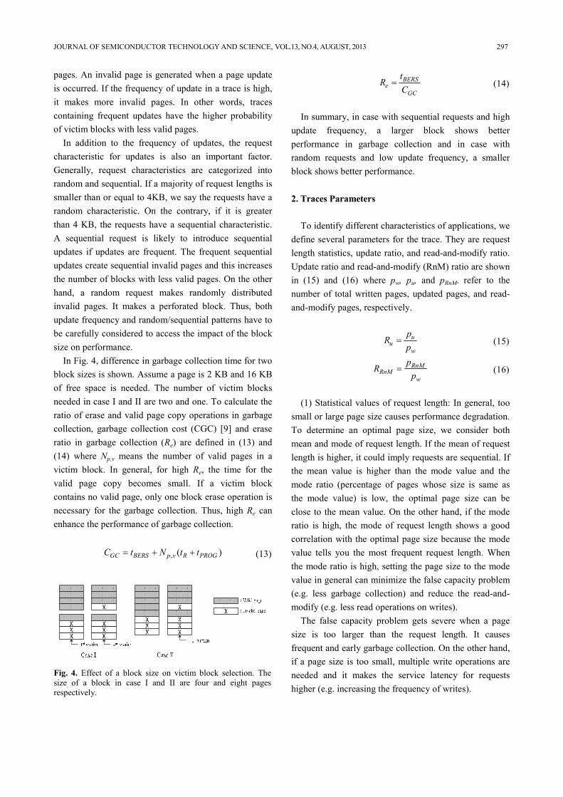
In Fig. 4, difference in garbage collection time for two
block sizes is shown. Assume a page is 2 KB and 16 KB
of free space is needed. The number of victim blocks
needed in case I and II are two and one. To calculate the
ratio of erase and valid page copy operations in garbage
collection, garbage collection cost (CGC) [9] and erase
ratio in garbage collection (Re) are defined in (13) and
(14) where Np,v means the number of valid pages in a
victim block. In general, for high Re, the time for the
valid page copy becomes small. If a victim block
contains no valid page, only one block erase operation is
necessary for the garbage collection. Thus, high Re can
enhance the performance of garbage collection.
, ( )GC BERS p v R PROGC t N t t= + + (13)
BERS
eGC
tR
C= (14)
In summary, in case with sequential requests and high
update frequency, a larger block shows better
performance in garbage collection and in case with
random requests and low update frequency, a smaller
block shows better performance.
2. Traces Parameters
To identify different characteristics of applications, we
define several parameters for the trace. They are request
length statistics, update ratio, and read-and-modify ratio.
Update ratio and read-and-modify (RnM) ratio are shown
in (15) and (16) where pw, pu, and pRnM. refer to the
number of total written pages, updated pages, and read-
and-modify pages, respectively.
u
uw
pR
p= (15)
RnM
RnMw
pR
p= (16)
(1) Statistical values of request length: In general, too
small or large page size causes performance degradation.
To determine an optimal page size, we consider both
mean and mode of request length. If the mean of request
length is higher, it could imply requests are sequential. If
the mean value is higher than the mode value and the
mode ratio (percentage of pages whose size is same as
the mode value) is low, the optimal page size can be
close to the mean value. On the other hand, if the mode
ratio is high, the mode of request length shows a good
correlation with the optimal page size because the mode
value tells you the most frequent request length. When
the mode ratio is high, setting the page size to the mode
value in general can minimize the false capacity problem
(e.g. less garbage collection) and reduce the read-and-
modify (e.g. less read operations on writes).
The false capacity problem gets severe when a page
size is too larger than the request length. It causes
frequent and early garbage collection. On the other hand,
if a page size is too small, multiple write operations are
needed and it makes the service latency for requests
higher (e.g. increasing the frequency of writes).
X XXXXX XXXX1 s t v i c t i m 2 n d v i c t i mX : V a l i d p a g e: I n v a l i d p a g e1 s t v i c t i mXXXX C a s e I C a s e I I
Fig. 4. Effect of a block size on victim block selection. The
size of a block in case I and II are four and eight pages
respectively.
298 KWANHU BANG et al : APPLICATION-AWARE DESIGN PARAMETER EXPLORATION OF NAND FLASH MEMORY
(2) Update Ratio Ru: Frequent updates to a page
generate many invalid pages. A victim block with many
invalid pages has a better garbage collection performance
because Re gets big. Let us assume two victim blocks
with different sizes have only invalid pages. They can be
erased without copying valid pages during garbage
collection. In this case, a larger block takes less time than
a smaller block to erase the same capacity because the
number of blocks to be erased is smaller. Thus, a larger
block shows better performance if the update ratio is high
and the number of valid pages in the victim block is
reasonably small.
(3) Read-and-Modify Ratio RRnM: As mentioned in
previous sections, read-and-modify(RnM) is triggered
when a update request is not aligned to a page boundary.
If the request length is smaller than the page size, RnM
always happens. Sequential requests are performed over
many pages and RnM happens only in the first and last
page. If traces have strong sequential characteristics,
RRnM decreases. In general, large RRnM increases time for
finishing service of a request because it increases the
frequency of read operations upon executing write
operations.
IV. EXPERIMENTAL RESULTS
1. Experimental Environments
To evaluate three metrics, performance (throughput),
cost, and power, we implement a trace-driven simulator
which takes traces and NFM design parameters as inputs
and generates a sequence of NFM operations and total
power consumption. Throughput and cost are computed
from the generated sequence of NFM operations and the
given NFM design parameters.
For the input traces of the simulator, we use both
synthetic traces and real traces. The purpose of the
synthetic traces is to isolate the effect of each design and
trace parameter. In synthetic traces, each trace represents
a different request length from 0.5 KB to 256 KB. To
provide the same garbage collection condition, the total
amount of written data is the same throughout all
synthetic traces. Thus a trace whose requests are shorter
has more requests.
Real traces are the ones collected by DiskMon [13]
from digital camera, file storage server, exchange server,
CrystalDiskMark random and sequential benchmark [14]
and general-purpose PC. The detailed characteristics of
the traces are shown in Table 3.
To compare throughput, cost, and power for NFMs
with different design parameters and traces, we
normalize the results to the one for the baseline NFM
configuration. From the prediction shown in Fig. 1, the
baseline is chosen as an NFM with a page size of 16 KB
and a block size of 512 pages.
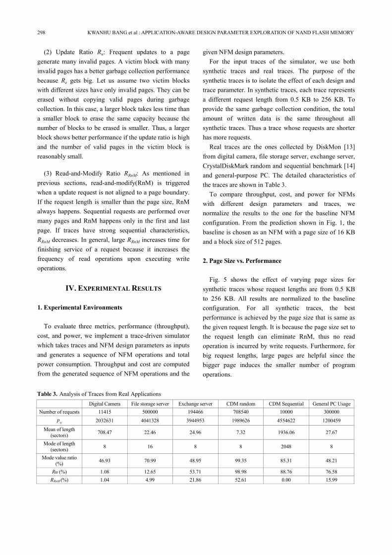
2. Page Size vs. Performance
Fig. 5 shows the effect of varying page sizes for
synthetic traces whose request lengths are from 0.5 KB
to 256 KB. All results are normalized to the baseline
configuration. For all synthetic traces, the best
performance is achieved by the page size that is same as
the given request length. It is because the page size set to
the request length can eliminate RnM, thus no read
operation is incurred by write requests. Furthermore, for
big request lengths, large pages are helpful since the
bigger page induces the smaller number of program
operations.
Table 3. Analysis of Traces from Real Applications
Digital Camera File storage server Exchange server CDM random CDM Sequential General PC Usage
Number of requests 11415 500000 194466 708540 10000 300000
pw 2032631 4041328 3944953 1989626 4554622 1200459
Mean of length
(sectors) 708.47 22.46 24.96 7.32 1936.06 27.67
Mode of length
(sectors) 8 16 8 8 2048 8
Mode value ratio
(%) 46.93 70.99 48.95 99.35 85.31 48.21
Ru (%) 1.08 12.65 53.71 98.98 88.76 76.58
RRnM (%) 1.04 4.99 21.86 52.61 0.00 15.99
JOURNAL OF SEMICONDUCTOR TECHNOLOGY AND SCIENCE, VOL.13, NO.4, AUGUST, 2013 299
Fig. 6 and 7 show the performance results for real
traces with various page sizes. In general, the best
performance is achieved when the page size is same as
the mode value of the request length distribution except
for the Digital Camera trace. This is because the number
of RnM is reduced when the page size is set to the mode
value. However, in case of Digital Camera trace, the 32
KB page leads to the best performance although its mode
value is 8 sectors (4 KB). It is due to its relatively low
mode value ratio. More specifically, since the number of
requests whose length is same as the mode value is small,
the optimal page size is determined not by the mode
value, but by the mean value as shown in Fig. 6. For
Exchange Server trace, a similar phenomenon is also
observed due to its low mode value ratio. But the trend is
not too visible due to the smaller difference between
mode and mean values. Although its optimal page size
should be 4 KB according to its mode value, the
performance of 4 KB page and 8 KB page are almost
same. It is because the mean value is bigger than 8 KB.
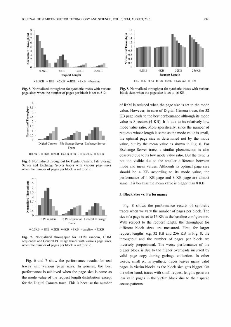
3. Block Size vs. Performance
Fig. 8 shows the performance results of synthetic
traces when we vary the number of pages per block. The
size of a page is set to 16 KB as the baseline configuration.
With respect to the request length, the throughput for
different block sizes are measured. First, for larger
request lengths, e.g. 32 KB and 256 KB in Fig. 8, the
throughput and the number of pages per block are
inversely proportional. The worse performance of the
bigger block is due to the higher overheads incurred by
valid page copy during garbage collection. In other
words, small Ru in synthetic traces leaves many valid
pages in victim blocks as the block size gets bigger. On
the other hand, traces with small request lengths generate
less valid pages in the victim block due to their sparse
access patterns.
0
1
2
3
4
5
6
7
8
9
0.5KB 4KB 32KB 256KB
Normalized Throughput
Request Length
0.5KB 1KB 2KB 4KB 8KB baseline
Fig. 5. Normalized throughput for synthetic traces with various
page sizes when the number of pages per block is set to 512.
0
0.5
1
1.5
2
2.5
3
3.5
4
Digital Camera File Storage Server Exchange Server
Normalized Throughput
Trace
0.5KB 1KB 2KB 4KB 8KB baseline 32KB
Fig. 6. Normalized throughput for Digital Camera, File Storage
Server and Exchange Server traces with various page sizes
when the number of pages per block is set to 512.
0
0.5
1
1.5
2
2.5
3
3.5
4
CDM random CDM sequential General PC usage
Normalized Throughput
Trace
0.5KB 1KB 2KB 4KB 8KB baseline 32KB
Fig. 7. Normalized throughput for CDM random, CDM
sequential and General PC usage traces with various page sizes
when the number of pages per block is set to 512.
0
0.2
0.4
0.6
0.8
1
1.2
1.4
1.6
1.8
0.5KB 4KB 32KB 256KB
Normalized Throughput
Request Length
16 32 64 128 256 baseline 1024
Fig. 8. Normalized throughput for synthetic traces with various
block sizes when the page size is set to 16 KB.
300 KWANHU BANG et al : APPLICATION-AWARE DESIGN PARAMETER EXPLORATION OF NAND FLASH MEMORY
Performance results for real traces are shown in Fig. 9
and 10. For traces whose performance is shown in Fig. 9,
performance decreases as the number of pages per block
increases. This is because Ru values of the traces are
relatively smaller than other traces as shown in Table 3.
In other words, the victim blocks upon garbage collection
contain many valid pages.
The trend of performance results shown in Fig. 10 is
different from that of Fig. 9. For CDM random and
sequential traces, the best performance is achieved with
the largest blocks whereas General PC usage trace shows
an optimal result when the block size is 128 pages. CDM
random and sequential traces have high Ru values, which
make victim blocks upon garbage collection contain a
small number of valid pages unlike three traces in Fig. 9.
Finally, General PC usage trace does not show any
dominant characteristic. Its Ru and request length are
moderate and thus its optimal block size is found at the
medium position.
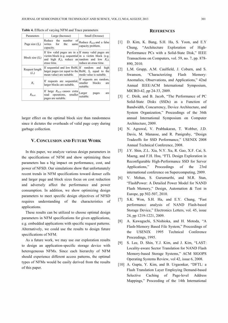
4. Cell Type Exploration
Fig. 11 compares SLC and MLC in terms of
performance, power and cost when General PC usage
trace is given as an input trace. Various metrics of MLC
are normalized to those of SLC. MLC shows worse
performance than SLC because it has a longer access
time. According to Table 2, MLC requires larger current
for a longer period of time, which leads to larger power
consumption. Both performance and power consumption
are highly correlated to the efficiency of garbage
collection. As a result, parameter optimization for less
garbage collection time guarantees better performance
and lower power consumption. On the other hand, the
cost of MLC is half the cost of SLC. Thus, optimizing
the cell type should consider what metric needs to be
optimized.
5. Summary of Experimental Results
Table 4 summarizes the findings based on our
experiments and analysis from a performance perspective.
First of all, results show Lr and Sp are closely related and
its relationship is strongly affected by RRnM. If RRnM is
high, which is usually caused by random access patterns,
the optimal page size is same as the mode value of
request length whereas for low RRnM, large page sizes
show the better performance.
From a performance perspective, the optimal block
size for a given trace is determined by two factors:
randomness (1/Lr) and Ru. Among two factors, Ru has the
0
2
4
6
8
10
12
14
16
Digital Camera File Storage Server Exchange Server
Normlized Throughput
Trace
16 32 64 128 256 baseline 1024
Fig. 9. Normalized throughput for Digital Camera, File Storage
Server and Exchange Server traces with various block sizes
when a page size is set to 16 KB.
0
0.2
0.4
0.6
0.8
1
1.2
CDM random CDM sequential General PC usage
Normalized Throughput
Trace
16 32 64 128 256 baseline 1024
Fig. 10. Normalized throughput for CDM random, CDM
sequential and General PC usage traces with various block
sizes when the page size is set to 16 KB.
00 . 5 11 . 522 . 533 . 544 . 55
16 64 256 1024 32 128 512 16 64 256 1024 32 128 512 16 64 256 1024 32 128 512 16 64 256 10240 . 5 K B 1 K B 2 K B 4 K B 8 K B 1 6 K B 3 2 K BN ormali zed met ri csofMLC
N F M c o n f i g u r a t i o nP e r f o r m a n c e P o w e r C o s t# o f p a g e sp e r b l o c kP a g e s i z e
Fig. 11. Performance, cost, and power of MLC normalized
SLC.
JOURNAL OF SEMICONDUCTOR TECHNOLOGY AND SCIENCE, VOL.13, NO.4, AUGUST, 2013 301
larger effect on the optimal block size than randomness
since it dictates the overheads of valid page copy during
garbage collection.
V. CONCLUSION AND FUTURE WORK
In this paper, we analyze various design parameters in
the specifications of NFM and show optimizing these
parameters has a big impact on performance, cost, and
power of NFSD. Our simulations show that unfortunately
recent trends in NFM specifications toward denser cells
and larger page and block sizes focus on cost reduction
and adversely affect the performance and power
consumption. In addition, we show optimizing design
parameters to meet specific design objectives of NFSD
requires understanding of the characteristics of
applications.
These results can be utilized to choose optimal design
parameters in NFM specifications for given applications,
e.g. embedded applications with specific request patterns.
Alternatively, we could use the results to design future
specifications of NFM.
As a future work, we may use our exploration results
to design an application-specific storage device with
heterogeneous NFMs. Since each hierarchy of NFM
should experience different access patterns, the optimal
types of NFMs would be easily derived from the results
of this paper.
REFERENCES
[1] D. Kim, K. Bang, S.H. Ha, S. Yoon, and E.Y
Chung, “Architecture Exploration of High-
Performance PCs with a Solid-State Disk,” IEEE
Transactions on Computers, vol. 59, no. 7, pp. 878-
890, 2010.
[2] L.M. Grupp, A.M. Caulfield, J. Coburn, and S.
Swanson, “Characterizing Flash Memory:
Anomalies, Observations, and Applications,” 42nd
Annual IEEE/ACM International Symposium,
MICRO-42, pp 24-33, 2009.
[3] C. Dirik, and B. Jacob, “The Performance of PC
Solid-State Disks (SSDs) as a Function of
Bandwidth, Concurrency, Device Architecture, and
System Organization,” Proceedings of the 36th
annual International Symposium on Computer
Architecture, 2009.
[4] N. Agrawal, V. Prabhakaran, T. Wobber, J.D.
Davis, M. Manasse, and R. Panigrahy, “Design
Tradeoffs for SSD Performance,” USENIX 2008
Annual Technical Conference, 2008.
[5] J.Y. Shin, Z.L. Xia, N.Y. Xu, R. Gao, X.F. Cai, S.
Maeng, and F.H. Hsu, “FTL Design Exploration in
Reconfigurable High-Performance SSD for Server
Applications,” Proceedings of the 23rd
international conference on Supercomputing, 2009.
[6] V. Mohan, S. Gurumurthi, and M.R. Stan,
“FlashPower: A Detailed Power Model for NAND
Flash Memory,” Design, Automation & Test in
Europe, pp 502-507, 2010.
[7] S.K. Won, S.H. Ha, and E.Y. Chung, “Fast
performance analysis of NAND Flash-based
Storage Device,” Electronics Letters, vol. 45, issue
24, pp 1219-1221, 2009.
[8] A. Kawaguchi, S.Nishioka, and H. Motoda, “A
Flash-Memory Based File System,” Proceedings of
the USENIX 1995 Technical Conference
Proceedings, 1995.
[9] S. Lee, D. Shin, Y.J. Kim, and J. Kim, “LAST:
Locality-aware Sector Translation for NAND Flash
Memory-based Storage Systems,” ACM SIGOPS
Operating Systems Review, vol 42, issue 6, 2008.
[10] A. Gupta, Y. Kim, and B. Urgaonkar, “DFTL: a
Flash Translation Layer Employing Demand-based
Selective Caching of Page-level Address
Mappings,” Proceeding of the 14th International
Table 4. Effects of varying NFM and Trace parameters
Parameters Large (Increase) Small (Dcrease)
Page size (Sp)
Reduce the number of
writes for the same
capacity.
Reduce RRnM and a false
capacity problem.
Block size (Sb)
If few valid pages are in a
victim block (e.g. sequential
and high Ru), reduce an
erase time.
If many valid pages are
in a victim block (e.g.
random and low Ru),
reduce an erase time.
Request length
(Lr)
If sequential and low RnM,
larger pages (or equal to the
mean value) are suitable.
If random and high
RnM, Sp equal to the
mode value is suitable.
Ru If requests are sequential,
larger blocks are suitable.
If requests are random,
smaller blocks are
suitable.
RRnM If large RRnM causes extra
read operations, smaller
pages are suitable.
Larger pages are
suitable.
302 KWANHU BANG et al : APPLICATION-AWARE DESIGN PARAMETER EXPLORATION OF NAND FLASH MEMORY
Conference on Architectural Support for Program-
ming Languages and Operating Systems, 2009.
[11] P. Rosenfeld, E. Cooper-Balis, B. Jacob, “DRAM-
Sim2: A Cycle Accurate Memory System Simulator,”
Computer Architecture Letters, vol 10, issue 1, pp
16-19, 2011.
[12] Hynix Semiconductor Inc., NAND Flash Datasheets,
http://www.hynix.com/gl/products/support/technical.jsp
[13] Windows Sysinternals, DiskMon, http://technet.
microsoft.com/en-us/sysinternals/
[14] Crystal Dew World, CrystalDiskMark. http://crystal-
mark.info/?lang=en
ACKNOWLEDGEMENTS
This work is supported by SK Hynix and by the National
Research Foundation of Korea(NRF) grant funded by the
Korea government(MEST) (No.2011-0023798, No.
2012-0007181, No. 2012-047670).
Kwanhu Bang received the B.S.
degrees in computer science and in
electronic engineering and the M.S.
degree in electrical and electronic
engineering from Yonsei University,
Seoul, Korea, in 2006 and 2008,
respectively. He is currently a Ph.D.
candidate in the School of Electrical and Electronic
Engineering at Yonsei University. His research interests
include biocomputation, flash memory applications, and
system-level low-power design.
Dong-gun Kim received the B.S.
and M.S. degrees in electrical and
electronic engineering from Yonsei
University in Seoul, Korea, in 2010
and 2012, respectively. He is an
Engineer with R&D division, SK
hynix Inc., Icheon, Korea. His
research interests include simulator development, next-
generation memory and system architecture.
Sang-Hoon Park received the B.S.
degree in electrical and electronic
engineering from Yonsei University
in Seoul, Korea, in 2009. He is a
Ph.D. candidate in Yonsei University.
His research interests include System
on Chip, NAND flash based mass
storage architecture and system architecture.
Eui-Young Chung received the B.S.
and M.S. degrees in electronics and
computer engineering from Korea
University, Seoul, Korea, in 1988
and 1990, respectively, and the Ph.D.
degree in electrical engineering from
Stanford University, Stanford, CA, in
2002. Until 2005, he was a Principal Engineer with SoC
R&D Center, Samsung Electronics, Yongin, Korea. He is
a Professor with the School of Electrical and Electronic
Engineering, Yonsei University, Seoul, Korea. His
research interests include system architecture, bio-
computing, and VLSI design.
Hyuk-Jun Lee received the B.S.
degree in computer science and
engineering from the University of
Southern California, Los Angeles, in
1993 and the M.S. and Ph.D. degrees
in electrical engineering from
Stanford University, Stanford, CA, in
1995 and 2001, respectively. From 2001 to 2011, he was
a senior engineer at Cisco Systems, San Jose, CA, USA.
He is currently an Assistant Professor with School of
Computer Science and Engineering, Sogang University,
Seoul, Korea. His research interests include computer
architecture, embedded systems, high-performance
memory systems, and network algorithms.


![SSD - ESOS LAB€¦ · SSD . 1 SSD Block Diagram 3.2 SSD NAND HDD . . SSD FTL . FTL NAND out-of-place update address mapping . Gabage Collection, Wear-leveling . 4. 4.1 SSD . Disksim[8]](https://img.pdfslide.net/doc/110x75/5ea6b67696cb1838a26c1ab1/ssd-esos-ssd-1-ssd-block-diagram-32-ssd-nand-hdd-ssd-ftl-ftl-nand-out-of-place.jpg)


![[Www.fisierulmeu.ro] rns 510 replacing hdd with ssd diy](https://img.pdfslide.net/doc/110x75/559a61bc1a28ab24698b45ce/wwwfisierulmeuro-rns-510-replacing-hdd-with-ssd-diy.jpg)