Embed Size (px)
Citation preview

Figure 1. PeakSwitch PKS606Y, 32 W Average, 81 W Peak, Universal Input Power Supply.
IntroductionThe PeakSwitch family is a highly integrated, monolithic, off-line switcher IC designed for use in power supplies that have to deliver peak loads for short durations. Example applications include inkjet printers, audio amplifiers and DVRs. When peak power is required, the effective switching frequency can approach 277 kHz, allowing a transformer with a small core size to be used. Innovative proprietary features, such as adaptive switching cycle on-time control, adaptive current limit, AC line sense and fast AC reset greatly simplify the design. This reduces engineering design time and system cost while providing complete system-level protection and robust functionality.
Each member of the family has a high-voltage power MOSFET and its controller integrated onto the same die. Internal start-up bias current is drawn from a high-voltage current source connected to the DRAIN pin, eliminating the need for external start-up components. The internal oscillator is frequency
modulated (jitter) to reduce EMI. In addition, the ICs have integrated functions that provide system-level protection. The auto-restart function limits the dissipation in the MOSFET, the transformer and the output diode during overload, output short- circuit and open-loop conditions, while the auto-recovering hysteretic thermal shutdown function disables MOSFET switching during a thermal fault. On-time extension enables more power to be delivered at low line and extends hold-up time. The smart AC line sense and undervoltage lockout (UVLO) functions enable the IC to latch off whenever a fault activates the auto-restart function, and to be reset quickly after AC power is removed.
Power Integrations’ EcoSmart® technology enables supplies designed around the PeakSwitch family members to consume <300 mW of no-load power and to meet harmonized energy efficiency standards such as the California Energy Commission (CEC), EU and ENERGY STAR.
February2007
T1EE25
J1L
PE
N
30 V @1.07 A Cont.2.7 A Peak
RTN
D51N4007
D6FR106
D10UF4003
D8STPS3150
D91N4148
D71N4148
U2PC817X4
Q2FS202DA
J3PCB Term 18 AWGRTN Connected to PE via Flying Lead
Q12N3906
D1-D41N4007
L15.3 mH
L25.3 µH
R21.3 MΩ
R11.3 MΩ
R152.2 Ω
R422 Ω1/2 W
R310 kΩ1/2 W
R52.2 MΩ
R62.4 MΩ
R162.7 MΩ
R74.7 kΩ
R121 kΩ
R131 kΩ
R14100 Ω
R113 kΩ
R101.5 kΩ
R90.33 Ω
2 W
R868 Ω1/2 W
C3680 nF
X1
C1-C2100 pF
250 VAC
C174.7 nF1 kV
C647 µF35 V
C15100 nF50 V
C16100 nF
C12330 µF50 V
C101 nF
250 VACC11
330 pF
U1PKS606Y
C1347 µF16 V
C14220 nF50 V
C7100 nF400 V
C8220 nF50 V
C52.2 nF1 kV
VR11N4764A
100 V
VR21N5255B
28 V
VR31N5258B
36 V
1
9,10
7,8
4
5
3
2
C4150 µF400 V
F13.15 A
RT110 Ω
PI-4170-060706
tO
PeakSwitch
C191 nF, 250 VAC
D
S
EN/UV
BP
GND
ApplicationNoteAN-41
PeakSwitch®
DesignGuide

AN-41
Rev. E 02/07
2
OUTPUTPOWERTABLE
PRODUCT3
230VAC±15% 85-265VACAdapter
Cont.1Adapter
Peak2Adapter
Cont.1Adapter
Peak2
PKS603 P 13 W 32 W 9 W 25 WPKS604 P 23 W 56 W 16 W 44 WPKS604 Y/F 35 W 56 W 23 W 44 WPKS605 P 31 W 60 W 21 W 44 WPKS605 Y/F 46 W 79 W 30 W 58 WPKS606 P 35 W 66 W 25 W 46 WPKS606 Y/F 68 W 117 W 45 W 86 WPKS607 Y/F 75 W 126 W 50 W 93 W
ScopeThis application note is intended for engineers designing an isolated AC-DC flyback power supply using the PeakSwitch family of devices. It provides guidelines to enable the engineer to quickly select key components and also complete a suitable transformer design. To simplify the task, this application note refers directly to the PI Xls design spreadsheet that is part of the PI Expert™ power supply design software suite.
In addition to this application note, the reader may also find the PeakSwitch Reference Design Kit (RDK) (the RDK contains an engineering prototype board, engineering report and device sample) useful as an example of a working power supply. Further details on downloading PI Expert, obtaining an RDK and updates to this document can be found at www.powerint.com.
Quick StartReaders can use the following information to quickly design a transformer and select the components for a first prototype. Only the information described below needs to be entered into the PI Xls spreadsheet; other parameters will be automatically selected by the spreadsheet, based on a typical design. References to spreadsheet cell locations are provided in square brackets [cell reference].
• Enter AC input voltage range VACMIN, VACMAX and minimum line frequency fL [B3, B4, B5]
• Enter nominal output voltage VO [B6]• Enter minimum output voltage at peak load assuming an
output drop is acceptable (if applicable) [B7]• Enter maximum output current at peak load or maximum
continuous load as applicable [B5]• Enter continuous (average) output power [B9]• Enter efficiency estimate:
0.7 for universal input voltage (85-265 VAC) or single 100/115 VAC (85-132 VAC) line voltage, and 0.75 for single 230 VAC (185-265 VAC) line voltage designs. Adjust the efficiency estimate accordingly, after measuring the efficiency of the first prototype-board at peak load and VACMIN. [B11]
• Enter loss allocation factor Z [B12]:
0.65 for typical application (adjust the number accordingly after first proto-board evaluation)
• Enter CIN input capacitance [B14]:
Use 2 µF/WPK for universal (85-265 VAC) or single (100/115 VAC) line voltage, if output voltage droop is acceptable, or 3 µF/WPK if output voltage droop is unacceptable.
Use 1 µF/WPK single 230 VAC for a single (185- 265 VAC) high-line voltage.
• Select PeakSwitch from drop down list or enter directly [B17]:
Select the device in the table below according to output power and line input voltage.
• Enter VD – forward voltage drop of the output diode [B25]:
0.5 V for Schottky diode 0.7 V for PN diode
• Enter core type (if desired) from drop down menu [B43]: A suggested core size will be selected automatically by the spreadsheet if none is entered.
• Build transformer• Select key components (see Steps 5 through 10)• Build prototype, test and iterate the design as necessary,
entering measured values into the spreadsheet where estimates were initially used (e.g. efficiency, VMIN)
Table 1. Output Power Table (See Data Sheet for Notes 1, 2 and 3).

AN-41
Rev. E 02/07
3
Step-by-StepTransformerDesignProcedureIntroduction
PeakSwitch devices have current limit values that allow the supply to deliver the specified peak power given in the power table. With sufficient heatsinking, these power levels could be provided continuously. However, PeakSwitch is optimized for use in applications that demand short duration, high peak power, while delivering a significantly lower continuous power. Typical peak-to-continuous ratios would be PPEAK ≥ 2 × PAVE. The high switching frequency of PeakSwitch allows a small core size to deliver the peak power but the short duration prevents the transformer windings from overheating and reduces heatsinking requirement for the device.
As the average power increases, based on the measured transformer temperature, it may be necessary to select a larger transformer so that the current density of its windings can be decreased.
The power table provides some guidance for peak and continuous (average) power levels in sealed adapters, although specific applications may vary. For example, if the peak power condition is of very low duty cycle, such as a two-second peak occurring at power up to accelerate a hard disk drive, then the temperature rise of the transformer is a function of the continuous power. However, if the peak power occurs every 200 ms for 50 ms, then peak power heating effects would need to be considered.
Figure 2 shows how to calculate the average power requirements for a design with two different peak load conditions.
Where Px represents the different output power conditions, Dtx represent the durations of each peak power condition and T is the period of one cycle of the pulsed load condition.
The design procedure requires both peak and continuous powers to be specified. The peak power is used to select the PeakSwitch device and design the transformer for power delivery at minimum input line voltage while continuous power (or average power if the peak load is periodic) is used for thermal design and may affect the size of the transformer and the heat sink.
Step1.EnterApplicationVariablesVACMIN,VACMAX,fL,VO,IO,VOatPeakLoad,h,Z,tC,CIN
Determine the input voltage range from Table 2.
PI-
4329
-030
906
P3
Power (W)
Time (t)
T
∆t1 ∆t2
P2
P1
Figure 2. Continuous (Average) Output Power Calculation Example.
Figure 3. Application Variable Section of PeakSwitch Design Spreadsheet.
NominalInputVoltage(VAC) VACMIN VACMAX
100/115 85 132230 195 265
Universal 85 265
Table 2. Standard Worldwide Input Line Voltage Ranges.
( ) ( )
,
P P P P P P
Tt
Tt
AVE 1 3 1 1 2 1 2
11
22
$ $= + - + -
= =
d d
d dD D
ENTER APPLICATION VARIABLES AN41 Example
VACMIN 85 Volts Minimum AC Input Voltage
VACMAX 265 Volts Maximum AC Input VoltagefL 50 Hertz AC Mains FrequencyNominal Output Voltage (VO) 24.00 Volts Nominal Output Voltage (at continuous power)Maximum Output Current (IO) 0.75 Amps Power Supply Output Current (corresponding to peak power)
Minimum Output Voltage at Peak Load 24.00 VoltsMinimum Output Voltage at Peak Power (Assuming output droop during peak load)
Continuous Power 6.00 6.00 Watts Continuous Output PowerPeak Power 18.00 Watts Peak Output Power
n 0.70Efficiency Estimate at output terminals and at peak load. Enter 0.7 if no better data available
Z 0.60 Loss Allocation Factor (Z = Secondary side losses / Total losses)tC Estimate 3.00 mSeconds Bridge Rectifier Conduction Time EstimateCIN 47.00 47 uFarads Input Capacitance

AN-41
Rev. E 02/07
4
Line Frequency, fL47 Hz for universal or 100/115 VAC input. 47 Hz for single 230 VAC input. For half-wave rectification use fL/2. For DC input enter the voltage directly into Cells B55 and B56.
Nominal Output Voltage, VO (V)Enter the nominal output voltage of the main output during the continuous load condition. Generally, the main output is the output from which feedback is derived.
Output Current, IO (A)Enter the maximum output current under peak load conditions. If the design does not have a peak load condition, then enter the maximum continuous output current. In multiple output designs, the output current of the main output (typically, the output from which feedback is taken) should be increased such that the peak power (or maximum continuous power as applicable) matches the sum of the output powers from all of the supply’s outputs. The individual output voltages and currents should then be entered at the bottom of the spreadsheet [cells B98 to B131].
Minimum Output Voltage at Peak Load (V)The output voltage may be specified in PeakSwitch designs based on whether or not the output voltage is allowed to droop during peak loads. If the application requires the output to remain the same under continuous and peak load conditions, leave this cell empty. The spreadsheet then assumes that the output voltage under peak load conditions is equal to the nominal output voltage, i.e. the output is not allowed to droop under peak load.
If the application allows the output voltage to droop under peak load conditions, enter the minimum acceptable voltage at peak load. The peak power is then calculated based on the output current and the minimum acceptable output voltage. In multiple output designs, if the main output is allowed to droop then all the other output voltages will also droop proportionally under peak load conditions.
Continuous Output Power (W)Enter the continuous output power. If this entry is left blank the design spreadsheet assumes that the continuous power is equal to the peak output power. This value is used by the spreadsheet to suggest a core size.
Peak Power (W)This is a calculated value based on the minimum output voltage at peak load, and maximum output current. It is used to calculate the required value of the primary inductance.
Power Supply Efficiency, hEnter the estimated efficiency of the complete power supply, measured at the output terminals under peak load conditions and worst-case line (generally lowest input voltage). Start
with a value of 0.7 (typical) for a design where the majority of the output power is drawn from an output voltage of 12 V or greater, and no current sensing is present on the secondary. Once a prototype has been constructed, the measured efficiency should be entered and the design of the transformer should be iterated.
Power Supply Loss Allocation Factor, ZThis factor represents the proportion of losses between the primary and the secondary of the power supply. Z factor is used together with the efficiency number, to determine the actual power that must be delivered by the power stage. For example, losses in the input stage (EMI filter, rectification, etc) are not processed by the power stage (transferred through the transformer), and therefore, although they reduce efficiency, the transformer design is not impacted.
For designs that do not have a secondary current sense circuit, enter 0.65. For those designs that do have a secondary current sense circuit, use a value of 0.7 until measurements can be made on a prototype. The higher number indicates larger secondary side losses associated with the secondary side current sense resistor.
Bridge Diode Conduction Time, tC (ms)Enter a bridge diode conduction time of 3.75 ms, if there is no better data available.
Total Input Capacitance, CIN (µF)Enter the total input capacitance, using Table 3 for guidance.
The capacitance is used to calculate the minimum DC voltage and should be selected to keep the minimum DC input voltage (VMIN) >70 V.
For designs that have a DC rather than an AC input, the value of the minimum and maximum DC input voltages, VMIN and VMAX, may be entered directly into the override cells on the design spreadsheet shown below.
TotalInputCapacitanceperWattOutputPower(µF/W)
AC Input Voltage (VAC)
Full Wave Rectification
100/115 3230 1
85-265 3
Table 3. Suggested Total Input Capacitance for Different Input Voltage Ranges.
AN-41
Rev. E 02/07
5
Step2–EnterPeakSwitchVariables:PeakSwitchDevice,VOR,VDS,VD,VDB,VCLO,KP(STEADYSTATE),KP(TRANSIENT)
Select the correct PeakSwitch deviceRefer to Table 1 and first select a device based on the peak output power of the design. Then compare the continuous power rating to the continuous numbers in the power table. If the continuous power exceeds the value given in the power table, then the next largest device should be selected. Similarly, if the continuous power is close to the power table’s power levels, then it may be necessary to switch to a larger device based on the measured thermal performance of the prototype.
Peak Load Switching Frequency, fs(min) (Hz)This parameter is the worst-case minimum switching frequency based on the minimum data sheet value of I2f (not adjustable).
Reflected Output Voltage, VOR (V)This parameter is the secondary winding voltage during the diode conduction time, which is reflected back to the primary through the turns ratio of the transformer. The default value is 110 V, however the acceptable range for VOR is between 80 V and 135 V, providing that no warnings are produced by the spreadsheet. For design optimization purposes, the following should be kept in mind:
1. Higher VOR allows increased power delivery at VMIN, which minimizes the value of the input capacitor and the droop of the output voltage when the on-time extension feature is used, and maximizes the power delivery from a given PeakSwitch device.
2. Higher VOR reduces the voltage stress on the output diodes, which in some cases may allow a Schottky diode to be used, and will thus give higher efficiency.
3. Higher VOR increases the leakage inductance of the transformer, which reduces efficiency of the power supply.
4. Higher VOR increases the peak and RMS currents on the secondary side, which may increase secondary side copper and diode losses.
Optimal selection of the VOR value should be based on a reasonable engineering compromise of the factors mentioned above.
PeakSwitch On-State Drain to Source Voltage, VDS (V)This parameter is the average on-state voltage developed across
the DRAIN and SOURCE pins of the PeakSwitch device. By default, if the grey override cell is left empty, a value of 10 V is assumed for Y/F package devices, and 5 V for P package devices. Use the default value if no better data is available.
Output Diode Forward Voltage Drop, VD (V)Enter the average forward voltage drop of the (main) output diode. Use 0.5 V for a Schottky diode or 0.7 V for a PN diode, if no better data is available. The spreadsheet uses a default value of 0.7 V.
Nominal Clamp Voltage, VCLO (V)Enter the nominal clamp voltage. The clamp is used to ensure that maximum voltage developed across the DRAIN and SOURCE pins of the internal MOSFET remains below the BVDSS specification (700 V) limit, with sufficient margin. It is recommended that a Zener diode with a value of 200 V be used in the clamp circuit. Even if an RCD clamp is used, a Zener should be placed in parallel with the RCD circuit to provide hard clamping during fault conditions. By default, if the grey override cell is left empty, a value of 200 V is assumed, which is also the maximum value recommended. Lower values can
Figure 4. DC Input Voltage Parameters Showing Grey Override Cells for DC Input Designs.
Figure 5. PeakSwitch Section of Design Spreadsheet.
DC INPUT VOLTAGE PARAMETERSVMIN 80 Volts Minimum DC Input VoltageVMAX 375 Volts Maximum DC Input Voltage
ENTER PeakSwitch VARIABLESPeakSwitch PKS603P PKS603P PeakSwitch deviceChosen Device PKS603PILIMITMIN 0.750 Amps Minimum Current LimitILIMITMAX 0.870 Amps Maximum Current LimitfSmin 250000 Hertz Minimum Device Switching Frequency
I^2fmin 164 A^2kHzI^2f (product of current limit squared and frequency is trimmed for tighter tolerance)
VOR 110 Volts Reflected Output Voltage (VOR <= 135 V Recommended)VDS 10 Volts PeakSwitch on-state Drain to Source Voltage VD 0.7 Volts Output Winding Diode Forward Voltage DropVDB 0.7 Volts Bias Winding Diode Forward Voltage DropVCLO 200 Volts Nominal Clamp Voltage KP (STEADY STATE) 0.60 Ripple to Peak Current Ratio (KP < 6)
KP (TRANSIENT) 0.38Ripple to Peak Current Ratio under worst case at peak load (0.25 < KP < 6)

AN-41
Rev. E 02/07
6
be used, as the VOR is reduced from 135 V, and/or in designs with low effective (primary and reflected secondary) leakage inductance values.
Ripple to Peak Current Ratio, KP (STEADYSTATE) and KP (TRANSIENT)Below a value of 1, indicating continuous conduction mode, KP is the ratio of ripple to peak primary current (Figure 6).
Above a value of 1, indicating discontinuous conduction mode, KP is the ratio of primary MOSFET off time to the secondary diode conduction time.
The value of KP should be in the range of 0.25 < KP < 6 and guidance is given in the comments cell if the value is outside this range.
KP (STEADY STATE) is the calculated KP value under the condition where several switching cycles have occurred consecutively.
KP (TRANSIENT) is the calculated minimum KP value that occurs after a switching cycle has been skipped. When the drain current starts from zero and ramps to the current limit, the on time for this first cycle is much longer than during steady state operation. This reduces the off time, reducing the time for the magnetizing inductance to reset, and causing the next cycle to start with a much higher initial current, a lower ripple current and a lower value of KP.
IR
KP ≡ KRP =IR
IP
(a) Continuous, KP < 1
(b) Borderline Continuous/Discontinuous, KP = 1
Primary
Primary
IR
IP
IP
PI-2587-011400
Figure 6. Continuous Mode Current Waveform, KP ≤1.
Figure 7. Discontinuous Mode Current Waveform, KP ≥1.
KDP =KP ≡(1-D) x T
t
(b) Borderline Discontinuous/Continuous, KP = 1
(a) Discontinuous, KP > 1
Secondary
Primary
Primary
Secondary
PI-2578-100606
D x T
D x T
t
(1-D) x T
(1-D) x T = t
T = 1/fS
T = 1/fS

AN-41
Rev. E 02/07
7
Figure 8 provides an illustration of the difference between transient and steady state KP. It shows a series of drain current waveforms for a design that does not meet KP (TRANSIENT) limits.
In region (a) the KP is stable with a value of 0.38. In region (b) the control loop has caused a switching cycle to be skipped, allowing the flux in the transformer core to be completely reset as the output diode is allowed to conduct for a much longer duration than in region (a). On the next switching cycle (c), the feedback loop has enabled a switching pulse and the current ramps from zero rather than some initial value. This means that the on-time for switching cycle (c) is much longer than for (a), allowing less off-time (the time during which the output diode conducts), yielding less resetting of the core flux. Therefore, cycle (d) starts with a much larger initial current pedestal than during the steady state conditions of (a). In the following cycles, (e) and (f), the value of KP settles again to the KP (STEADY STATE) of 0.38.
The sequence of skipped cycle (b) followed by a cycle that gives the minimum possible off time (c) is where the spreadsheet calculates the value of KP (TRANSIENT). In this example, KP (TRANSIENT) is 0.19, below the 0.25 limit and is thus unacceptable. To address this problem a larger device could be selected, the VOR increased, or the output power reduced.
KP (TRANSIENT) should be above a value of 0.25 to prevent the large initial current pedestal from falsely triggering current limit at the end of the leading edge blanking time and limiting power delivery. Similar guidance is given in the comment cell on how to maintain KP (TRANSIENT) within acceptable limits.
Step 3 – Enter Under-Voltage Lock Out (UVLO)Variables,V_UV_TARGET(V)
The line under-voltage lockout feature of PeakSwitch sets the minimum startup voltage of the supply, prevents the power supply output from glitching when the input voltage is below the normal operating range, and is used to determine if the supply should latch off during a fault. Connecting a resistor from an input capacitor to the EN/UV pin enables this feature. Enter the desired DC voltage across the input capacitor, at which the power supply should start operating. The spreadsheet calculates both the ideal resistor value and closest standard value, together with the typical start-up voltage based on the closest standard value (Figure 9). Either a resistor with a voltage rating >375 V or two series resistors whose voltage rating sum is >375 V should be used.
Step4–ChooseBiasWindingOutputVoltage,VB(V)
By default, if the grey override cell is left empty, a value of 15 V is assumed. The user can override this value as needed. However, the value should be in the range of 8 V <VB <20 V. The lower value ensures adequate headroom for supplying current into the BYPASS pin. The upper value limits the no-load input power consumption caused by high power consumption in the bias winding. The number of bias winding turns, NB, is to be used for transformer construction. An ultra-fast diode with a voltage rating above the calculated PIVB value should be selected. Select the value of resistor from the bias supply to the BYPASS pin to provide the maximum data sheet supply current for the selected PeakSwitch device.
IR = 0.3 AIP = 0.8 AKP = 0.38
IR = 0.3 AIP = 0.8 AKP = 0.38
Drain CurrentSecondary (Diode) CurrentSkipped Cycle
(a) (b) (c) (d) (e) (f)
IR = 0.8 AIP = 0.8 AKP = 1
IR = 0.15 AIP = 0.8 AKP = 0.19
IR = 0.38 A IP = 0.8 AKP = 0.48
IR = 0.28 A IP = 0.8 AKP = 0.35
IR = 0.3 A IP = 0.8 AKP = 0.38
PI-4337-031706
Figure 8. Drain Current Waveform Illustrating KP(STEADY STATE) and KP(TRANSIENT).
Figure 9. Under-Voltage Variables Section of Design Spreadsheet.
Figure 10. Bias Winding Variables Section of Design Spreadsheet.
ENTER UVLO VARIABLES
V_UV_TARGET 88 VoltsTarget DC under-voltage threshold, above which the power supply with start
V_UV_ACTUAL 85 VoltsTypical DC start-up voltage based on standard value of RUV_ACTUAL
RUV_IDEAL 3.45 Mohms Calculated value for UV Lockout resistorRUV_ACTUAL 3.30 Mohms Closest standard value of resistor to RUV_IDEAL
BIAS WINDING VARIABLESVB 15.00 Volts Bias winding VoltageNB 10 Number of Bias Winding TurnsPIVB 68 Volts Bias rectifier Maximum Peak Inverse Voltage

AN-41
Rev. E 02/07
8
Step5–ChooseCoreandBobbinBasedonOutputPower,andEnterAE,LE,AL,BW,M,L,NS
Core effective cross-sectional area, AE: (cm2)Core effective path length, LE: (cm).Core ungapped effective inductance, AL: (nH/turn2).Bobbin width, BW: (mm)Tape margin width equal to half the total margin, M (mm)Primary Layers, LSecondary Turns, NS
Core TypeBy default if the core type cell is left empty, the spreadsheet will select the smallest commonly available core suitable for the continuous output power. Available cores can be selected from the drop down list in the tool bar of the PI Xls design software. The grey override cells can be used to enter the core and bobbin parameter directly by a user. This is useful if the user wants to use a core that is not on the list, or the specific core or bobbin information differs from that recalled by the spreadsheet.
Safety Margin, M (mm)For designs that require isolation but are not using triple insulated wire, the width of the safety margin to be used on each side of the bobbin should be entered here. For universal input designs, a total margin of 6.2 mm would be required, and a value of 3.1 mm would be entered into the spreadsheet. For vertical bobbins, the margin may not be symmetrical. However if a total margin of 6.2 mm were required, then 3.1 mm would still be entered even if the physical margin is only on one side of the bobbin.
For designs using triple insulated wire, it may still be necessary to enter a small margin in order to meet the required safety creepage distances. Many bobbins exist for each core size, and each will have different mechanical spacing. Refer to the specific bobbin data sheet or seek guidance from your safety expert or transformer vendor to determine what specific margin is required.
Since margin construction reduces the available area for the windings, it may not be suitable for small core sizes. If after entering the margin, more than three primary layers (L) are
required, either a larger core should be selected, or consider a zero margin design using triple insulated wire.
Primary Layers, LBy default, if the override cell is empty, a value of 3 is assumed. Primary layers should be in the range of 1 < L < 3 and in general it should be the lowest number that meets the primary current density limit of 100 Cmils/Amp (CMA). More than three layers are possible, but the increased leakage inductance and physical fit of the windings should be considered. Due to the
high switching frequency of PeakSwitch designs, it is important to minimize transformer leakage inductance. Therefore split primary construction is recommended for all designs regardless of power level. In split primary construction, half of the primary winding is placed on either side of the secondary and bias windings, in a sandwich arrangement.
Secondary Turns, NSBy default, if the grey override cell is left blank, the minimum number of secondary turns is calculated such that the maximum operating flux density BM is kept below the recommended maximum of 3000 Gauss (300 mT). In general it is not necessary to enter a number in the override cell except in designs where a lower operating flux density is desired (see the explanation of BM limits).
Step 6 – Iterate Transformer Design and GenerateInitialDesign
Iterate the design making sure that no warnings are displayed. Any parameters outside the recommended range of values can be corrected by following the guidance given in the right hand column.
Once all warnings have been cleared, the output transformer design parameters can be used to either wind a prototype transformer or sent to a vendor for samples.
The key transformer electrical parameters are:
Primary Inductance, LP (µH)This is the target nominal primary inductance of the transformer.
Figure 11. Transformer Variables Section of Design Spreadsheet.
ENTER TRANSFORMER CORE/CONSTRUCTION VARIABLES
Core Type Auto EE13Transformer Core (Verify acceptable thermal rise under continuous load conditions)
Core EE13 P/N: PC40EE13-ZBobbin EE13_BOBBIN P/N: EE13_BOBBINAE 0.171 cm^2 Core Effective Cross Sectional AreaLE 3.02 cm Core Effective Path LengthAL 1130 nH/T^2 Ungapped Core Effective InductanceBW 7.90 mm Bobbin Physical Winding Width
M 0.00 mmSafety Margin Width (Half the Primary to Secondary Creepage Distance)
L 3 Number of Primary LayersNS 16 Number of Secondary Turns

AN-41
Rev. E 02/07
Primary Inductance Tolerance, LP_TOLERANCE(%)This is the assumed primary inductance tolerance. A value of 12% is used by default. However, if specific information is known from the transformer vendor, then this may be entered in the grey override cell.
Number of Primary Turns, NPTotal number of primary turns. For low leakage inductance it is recommended that split primary construction be used.
Gapped core effective inductance, ALG (nH/T2) used by the transformer vendor to specify the core gap.
Target BM (Gauss)The value entered here is used to calculate the number of secondary turns. By default, a value of 2800 Guass is used, slightly below the recommended maximum BM value of 3000 Gauss. This accounts for the rounding down of the number of calculated secondary turns in some designs.
Maximum Operating Flux Density, BM (Gauss)A maximum value of 3000 Gauss during normal operation is recommended to limit the maximum flux density under start up and output short circuit. Under these conditions, the output voltage is low and little reset of the transformer occurs during the MOSFET off time. This may allow the transformer flux density to staircase above the normal operating level. A value of 3000 Gauss at the peak current limit of the selected device, together with the built-in protection features of PeakSwitch provides sufficient margin to prevent core saturation under startup or output short circuit conditions.
The cycle skipping mode of operation used in PeakSwitch can produce audio frequency displacements in the transformer. To limit this noise, the transformer should be designed such that the peak core flux density is below 3000 Gauss (300 mT). Following this guideline and using the standard transformer production technique of dip varnishing practically eliminates audible noise. A careful evaluation of the audible noise performance should be made, using production transformer samples before approving the design. When ceramic capacitors that have Z5U dielectrics are used in clamp circuits, they too may produce audible sound. They should be replaced with capacitors that have a different dielectric, such as polyester film.
Maximum Primary Wire Diameter, OD (mm)By default, if the override cell is empty, double coated wire is assumed and a standard wire diameter is chosen. The grey override cells can be used to enter a wire diameter directly.
Primary wire size, DIA: (mm)Primary wire gauge, AWGNumber of primary layers, LEstimated core center leg gap length: Lg: (mm)Number of secondary turns, NSSecondary wire size, DIAS: (mm)Secondary wire gauge, AWGS
In multiple output designs NSx, CMSx, AWGSx (where x is the output number) should also be used.
Figure 12. Transformer Primary Design Section of Design Spreadsheet.
Figure 13. Transformer Secondary Primary Parameters Section of Design Spreadsheet – Lumped into Single Output.
TRANSFORMER PRIMARY DESIGN PARAMETERS
LP 367 uHenriesTypical Primary Inductance. +/- 12% to ensure a minimum primary inductance of 328 uH
LP_TOLERANCE 12 % Primary inductance tolerance
NP 71 Primary Winding Number of TurnsALG 72 nH/T^2 Gapped Core Effective InductanceTarget BM 2800 Gauss Target Peak Flux Density at Maximum Current Limit
BM 2624 GaussCalculated Maximum Operating Flux Density, BM < 3000 is recommended
BAC 789 Gauss AC Flux Density for Core Loss Curves (0.5 X Peak to Peak)ur 1588 Relative Permeability of Ungapped CoreLG 0.28 mm Gap Length (Lg > 0.1 mm)BWE 23.7 mm Effective Bobbin WidthOD 0.33 mm Maximum Primary Wire Diameter including insulationINS 0.06 mm Estimated Total Insulation Thickness (= 2 * film thickness)DIA 0.28 mm Bare conductor diameter
AWG 30 AWGPrimary Wire Gauge (Rounded to next smaller standard AWG value)
CM 102 Cmils Bare conductor effective area in circular milsCMA 208 Cmils/Amp Primary Winding Current Capacity (100 < CMA < 500)
TRANSFORMER SECONDARY DESIGN PARAMETERS Lumped parametersISP 3.34 Amps Peak Secondary CurrentISRMS 1.74 Amps Secondary RMS CurrentIRIPPLE 1.57 Amps Output Capacitor RMS Ripple CurrentCMS 349 Cmils Secondary Bare Conductor minimum circular mils
AWGS 24 AWGSecondary Wire Gauge (Rounded up to next larger standard AWG value)
AN-41
Rev. E 02/07
10
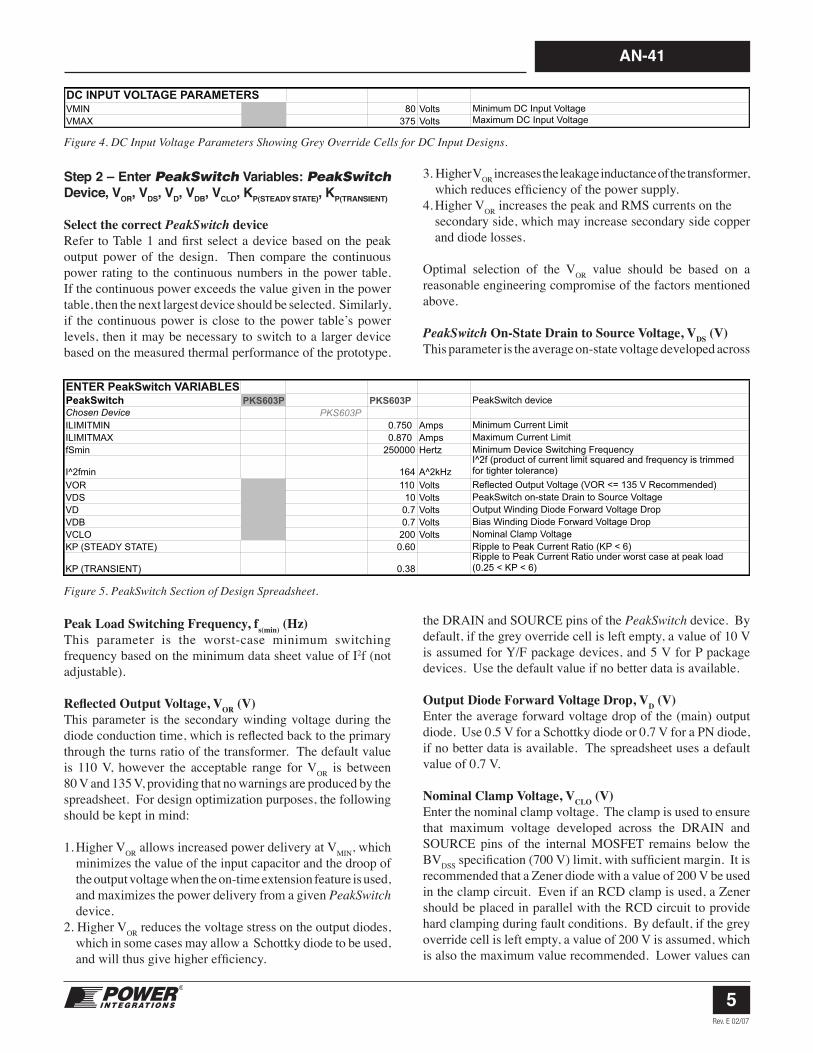
Figure 14. Transformer Secondary Design Parameters Section of Spreadsheet – Multiple Outputs.
Step 7 – Selection of PeakSwitch ExternalComponents
Bypass Pin CapacitorFor the BYPASS pin, use a 0.33 µF, 50 V ceramic capacitor or a 1 µF, 50 V electrolytic, whichever is lower cost.
Step8–SelectionofUnder-VoltageorACLineSenseComponents
UVLO prevents the supply from starting up prematurely, while latching shutdown protects the IC, the supply and the load from fault conditions. The rectified AC input voltage that forces the current into the EN/UV pin to exceed 25 µA sets the UVLO threshold.
For example, if regulation is lost due to a short circuit, an open loop or an output overload condition, and the input voltage is sufficient to support normal operation (>25 µA into the EN/UV pin), then PeakSwitch will latch off. To reset the latch, the AC input has to be removed long enough so that the current into the EN/UV pin falls below the 25 µA UV threshold. Once AC is reapplied, the next time the EN/UV pin current exceeds 25 µA, the supply will attempt to restart.
For some applications, the time for the EN/UV pin current to fall below 25 µA may be excessive due to the time for the bulk input capacitor to discharge. In such cases, a fast AC reset circuit can be used allowing latching shutdown to be independent of the load and voltage on the bulk input capacitor. This prevents
TRANSFORMER SECONDARY DESIGN PARAMETERS (MULTIPLE OUTPUTS)1st output
VO1 24 Volts Main Output Voltage (if unused, defaults to single output design)IO1 0.750 Amps Output DC CurrentPO1 18.00 Watts Output PowerVD1 0.7 Volts Output Diode Forward Voltage DropNS1 16.00 Output Winding Number of TurnsISRMS1 1.744 Amps Output Winding RMS CurrentIRIPPLE1 1.57 Amps Output Capacitor RMS Ripple CurrentPIVS1 108 Volts Output Rectifier Maximum Peak Inverse Voltage
Recommended DiodesBYV27-200 Recommended Diodes for this output
CMS1 349 Cmils Output Winding Bare Conductor minimum circular milsAWGS1 24 AWG Wire Gauge (Rounded up to next larger standard AWG value)DIAS1 0.51 mm Minimum Bare Conductor DiameterODS1 0.49 mm Maximum Outside Diameter for Triple Insulated Wire
2nd outputVO2 Volts Output VoltageIO2 Amps Output DC CurrentPO2 0.00 Watts Output PowerVD2 0.7 Volts Output Diode Forward Voltage DropNS2 0.45 Output Winding Number of TurnsISRMS2 0.000 Amps Output Winding RMS CurrentIRIPPLE2 0.00 Amps Output Capacitor RMS Ripple CurrentPIVS2 2 Volts Output Rectifier Maximum Peak Inverse VoltageRecommended Diode Recommended Diodes for this outputCMS2 0 Cmils Output Winding Bare Conductor minimum circular milsAWGS2 N/A AWG Wire Gauge (Rounded up to next larger standard AWG value)DIAS2 N/A mm Minimum Bare Conductor DiameterODS2 N/A mm Maximum Outside Diameter for Triple Insulated Wire
3rd outputVO3 Volts Output VoltageIO3 Amps Output DC CurrentPO3 0.00 Watts Output PowerVD3 0.7 Volts Output Diode Forward Voltage DropNS3 0.45 Output Winding Number of TurnsISRMS3 0.000 Amps Output Winding RMS CurrentIRIPPLE3 0.00 Amps Output Capacitor RMS Ripple CurrentPIVS3 2 Volts Output Rectifier Maximum Peak Inverse VoltageRecommended Diode Recommended Diodes for this outputCMS3 0 Cmils Output Winding Bare Conductor minimum circular milsAWGS3 N/A AWG Wire Gauge (Rounded up to next larger standard AWG value)DIAS3 N/A mm Minimum Bare Conductor DiameterODS3 N/A mm Maximum Outside Diameter for Triple Insulated Wire
Total power 18 Watts Total Output Power
Negative Output N/AIf negative output exists enter Output number; eg: If VO2 is negative output, enter 2
AN-41
Rev. E 02/07
11
race conditions that could cause unwanted triggering during brownout or on removal of the AC input.
Referring to Figure 1, the fast AC reset circuit is comprised of D5, C7, R5 and R6. The incoming AC is rectified by D5 and filtered by C7 with R5 and R6 providing the line sensing current into the EN/UV pin. When AC power is removed (after a fault has occurred and the unit has latched off), C7 discharges quickly via R5 and R6. The value of C7 is selected so that the current through R5 and R6 has fallen below the UV threshold (25 µA) after the desired reset time (~3 seconds as shown) has elapsed. The capacitor should have a voltage rating greater than VACMAX × √2, with 400 V metal film capacitors being a suitable choice.
If the line UVLO function and latching shutdown are desired and fast AC reset is not required, then the resistor value from step 3 can be connected from the UV/EN pin to the positive side of the input bulk capacitor.
If no resistors are fitted then the PeakSwitch device senses this condition and the UVLO function is disabled.
The sense resistor should be rated above 400 V, generally requiring either a single 0.5 W resistor or two 0.25 W resistors connected in series.
Step–SelectionofPrimaryClampComponents
It is recommended that either a Zener clamp or an RCD combined with a Zener clamp be used in PeakSwitch designs. This is to ensure that the peak drain voltage is limited to below the BVDSS of the internal MOSFET while still maximizing efficiency and minimizing no-load consumption.
A standard RCD clamp designed to limit the peak drain voltage under peak load conditions represents a significant load as the output power is reduced, resulting in low light load efficiency and high no-load consumption.
Figure 1 shows an example of an optimized clamp arrangement. The addition of VR1 in series with R3 prevents C5 from discharging below 100 V as the effective switching frequency lowers as the load is reduced. The value of R3 is selected so that the peak drain voltage is limited to an acceptable level under worst-case conditions of maximum input voltage, maximum ambient temperature and maximum overload power or a short circuit on the output of the supply.
The peak drain voltage should be limited to a maximum voltage of 650 V under these conditions to provide margin for component variation. In the sample design shown in these steps, the peak drain voltage was limited to 600 V. The clamp diode (D6) must
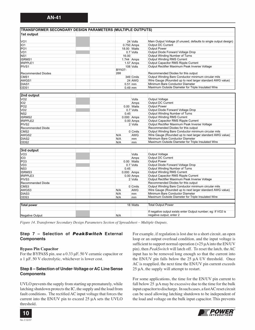
SeriesNumber TypeVRRange ID Package Manufacturer
V AIN5817 to 1N5819 Schottky 20-40 1 Leaded VishaySB120 to SB1100 Schottky 20-100 1 Leaded Vishay/Fairchild11DQ50 to 11DQ60 Schottky 50-60 1 Leaded IR1N5820 to 1N5822 Schottky 20-40 3 Leaded VishayMBR320 to MBR360 Schottky 20-60 3 Leaded IR/On SemiSS12 to SS16 Schottky 20-60 1 SMD VishaySS32 to SS36 Schottky 20-60 3 SMD VishaySB540 to SB560 Schottky 40-60 5 Leaded VishayUF4002 to UF4006 Ultrafast 100-600 1 Leaded VishayMUR110 to MUR160 Ultrafast 100-600 1 Leaded On SemiUF5401 to UF5408 Ultrafast 100-800 3 Leaded VishayES1A to ES1D Ultrafast 50-200 1 SMD VishayES2A to ES2D Ultrafast 50-200 2 SMD VishayBYV28-200 Ultrafast 200 3.5 Leaded VishayMBR745 to MBR760 Schottky 40-60 7.5 TO220 VishayMBR1045 to MBR10100 Schottky 45-100 10 TO220 VishayBYW29-100 to BYW29-200 Ultrafast 100-200 8 TO220 Vishay
Table 4. List of Diodes Suitable For Use as the Output Rectifier.

AN-41
Rev. E 02/07
12
be a fast or an ultra-fast recovery type with a reverse recovery time <500 ns. Under no circumstances should a slow recovery rectifier diode be used. The high dissipation that may result during startup or an output short circuit can cause failure of the diode. Resistor R4 dampens ringing for reduced EMI.
Supplies using different devices in the PeakSwitch family will have different peak primary current, leakage inductances and leakage energy. Therefore, C5 and R3 should be optimized for each design. As a general rule, minimize the value of capacitor C5 and maximize the value of resistor R3.
Step 10 – Select Output Rectifier Diode
For each output, use the values of peak inverse voltage (VR) and output current (IO) provided in the design spreadsheet to select the output diodes. Table 4 shows some commonly available types.
VR ≥ 1.25 × PIVS: where PIVS is taken from the Voltage Stress Parameters section of the spreadsheet and Transformer Secondary Design Parameters (Multiple Outputs).
ID ≥ 2 × IO: where ID is the rated DC current of the diode and IO is the average output current. Depending on the thermal rise and duration of the peak load condition, it may be necessary to increase the diode current rating once a prototype has been built. This also applies to the amount of heatsinking required.
Step11–SelectOutputCapacitor
Ripple Current RatingThe spreadsheet calculates the output capacitor ripple current at peak load. Therefore the actual rating of the capacitor will depend on the peak to average power ratio of the design. For a conservative design, select the output capacitor(s) such that the ripple rating is greater than the calculated value, IRIPPLE from the spreadsheet, calculated at the peak load condition. However in designs with high peak to continuous (average) power ratios, the capacitor rating can be reduced based on the measured temperature rise under worst-case load and ambient temperature. If a suitable individual capacitor cannot be found, then two or more capacitors may be used in parallel to achieve a combined ripple current rating equal to the sum of the individual capacitor ratings.
OutputVoltage(V)
ZenerValue,VRFB(V)
FeedbackBiasResistor,RBIAS
(kW)
OptoSeriesResistor,RFB1
(W)
FeedbackCapacitor,CFB1
(nF)SeriesDiode
DFBRequired?
5 4.3
1 220 100
No8 7.512 1118 16
Yes24 2230 28
PI-4338-031606
LPF
DFB
VRFB
RBIAS
CFB1
CPF
+VOUT
RTN
UFB1
COUT
RFB1
Table 5. Zener Feedback Arrangement and Typical Component Values.
AN-41
Rev. E 02/07
13
Many capacitor manufacturers provide factors that increase the ripple current rating as the capacitor operating temperature is reduced from its data sheet maximum value. This should be considered in order to ensure that the capacitor is not oversized.
ESR SpecificationThe switching ripple voltage is equal to the peak secondary current multiplied by the ESR of the output capacitor. It is therefore important to select low ESR capacitors to reduce the ripple voltage. In general, selecting a high ripple current rated capacitor results in an acceptable value of ESR.
Voltage RatingSelect a voltage rating such that VRATED ≥1.25 VO.
Step12–SelectFeedbackCircuitComponents
The feedback loop is arranged to draw the disable current (240 µA) from the EN/UV pin when the output voltage reaches regulation. Ideally, the feedback loop should be able to respond to the ripple on the output capacitor cycle-by-cycle.
Due to the high switching frequency, a high gain optocoupler of 300-600% is recommended to minimize feedback delay. Adding a capacitor across the DC gain setting resistor (R12 in Figure 1) further increases high frequency gain.
Table 5 shows a typical implementation of Zener feedback. The series drops across DFB, VRFB, RFB1 and the forward drop of the LED UFB1 determine the output voltage. Diode DFB is optional, depending on the availability of a suitable zener voltage. Resistor RBIAS provides a 1 mA bias current so that VRFB is operating close to its knee voltage. Resistor RFB1 sets the DC gain of the feedback. Both resistors can be 0.125 W or 0.25 W, 5%. To increase high frequency gain, a ceramic capacitor CFB1 is placed across RFB. Selecting a Zener with a low test current (5 mA) will minimize the current needed to bias the feedback network, reducing no-load input power consumption.
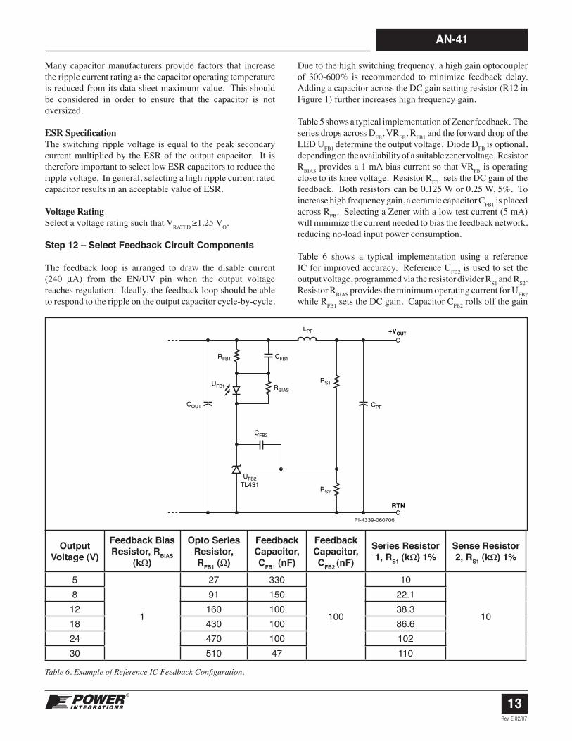
Table 6 shows a typical implementation using a reference IC for improved accuracy. Reference UFB2 is used to set the output voltage, programmed via the resistor divider RS1 and RS2. Resistor RBIAS provides the minimum operating current for UFB2 while RFB1 sets the DC gain. Capacitor CFB2 rolls off the gain
OutputVoltage(V)
FeedbackBiasResistor,RBIAS
(kW)
OptoSeriesResistor,RFB1(W)
FeedbackCapacitor,CFB1(nF)
FeedbackCapacitor,CFB2(nF)
SeriesResistor1,RS1(kW)1%
SenseResistor2,RS1(kW)1%
5
1
27 330
100
10
10
8 91 150 22.112 160 100 38.318 430 100 86.624 470 100 10230 510 47 110
Table 6. Example of Reference IC Feedback Configuration.
PI-4339-060706
LPF
RBIAS
RS1
RS2
CFB1RFB1
UFB1
CFB2
CPF
+VOUT
RTN
UFB2TL431
COUT

AN-41
Rev. E 02/07
14
of UFB2 so that it does not respond to the cycle-by-cycle output ripple voltage. AC feedback is provided directly through the optocoupler with CFB1 increasing the gain.
If necessary, a post filter (LPF and CPF) can be added to reduce high frequency switching noise and ripple. Inductor LPF should be in the range of 1 µH – 3.3 µH with a current rating above the peak output current. Capacitor CPF should be in the range of 100 µF to 330 µF with a voltage rating ≥1.25 × VOUT. If a post filter is used, the optcoupler should be connected (as shown in Table 6) before the post filter inductor, and the sense resistors after the post filter inductor (when applicable).
DesignTipsOvercurrent and Overvoltage Protection CircuitsIn some applications, it may be necessary to protect the load in fault conditions such as output overcurrent (OCP) or overvoltage (OVP). For example, if the load is a motor, then OCP can prevent the motor from overheating if it is stalled. Similarly, if the feedback loop is opened then the load can be protected from excessive voltage by overvoltage shutdown.
The smart AC sense feature of PeakSwitch simplifies implementation of such protection by providing the latching function on the primary side. Figure 15 shows a combined overcurrent and overvoltage shutdown circuit. The circuit is arranged so that if either overcurrent or overvoltage occurs, then SCR Q2 is turned on, shorting the output. Normally, this component would have to be sized to dissipate significant power. However, when the arrangement is used with PeakSwitch, the smart AC sense and latch-off feature will shut down the supply.
For OCP, resistor R1 senses the output current, turning on transistor Q1 when the voltage drop across R1 exceeds the VBE of Q1. Resistor R2 and C1 set a time constant allowing short term peak current but triggering the OCP in a true fault. Resistor R3 limits the current into the gate of Q2.
For OVP, Zener diode VR1 is selected such that it conducts when the output voltage exceeds the acceptable range, turning on Q2. Resistor R4 limits the Zener current and determines the turn-on point for Q2. Capacitor C2 provides decoupling, preventing false triggering of Q2 due to noise.
Transistor Q1 can be any small signal PNP bipolar transistor. The value of R1 is given by VBE(Q1) / IOCP, and power rating VBE(Q1) × IOCP where IOCP is the desired overcurrent trip point and VBE(Q1) is the base-emitter drop of Q1. The initial values of R2 and C1 are selected such that 3τ ≥ tTRIP where τ = R2 × C1 and tTRIP is the minimum trip time in seconds. Use a starting value of 1 kW for R2, then optimize based on measured trip time, as peak to continuous current levels affect actual timing. Select R3 to exceed the worst case gate trigger current of Q2, when Q1 conducts. Values of 1 kW to 4.7 kW are typical. Select the Zener voltage of VR1
PI-4340-031706
VR1
R4
R3
R2
C1
Q2
C2
+VOUT
RTN
Q1
R1
to be above the normal output voltage tolerance range, including the tolerance of VR1 itself. Resistor R4 is a 0.25 W, 100 W part and C2 is a small, 100 nF ceramic. SCR Q2 should be selected with a current rating above the continuous output current of the supply. For example for a 1 A output, a 2 A SCR would be a good choice. The anode of Q2 can be directly connected to the anode of the output diode, so that when fired, the secondary winding is shorted. This removes the need for the SCR to discharge the output capacitor and may allow a smaller current rating device to be selected. However, an additional ultra-fast diode must be placed in series with the SCR to block reverse current (see D10 in Figure 1).
In designs where the latching feature is not used, a larger current rating SCR may be required.
Transformer Core SizingThe high switching frequency of PeakSwitch allows the selection of small core sizes that will adequately process the peak power. However, the small core size reduces the amount of winding window area available. This reduces the amount of copper for the windings, increasing winding losses.
In designs where the ratio of peak to continuous power is low (<~2), the transformer size may need to be increased to reduce losses and transformer heating. Acceptable temperature rise of the transformer should be verified at worst-case ambient temperature and maximum load.
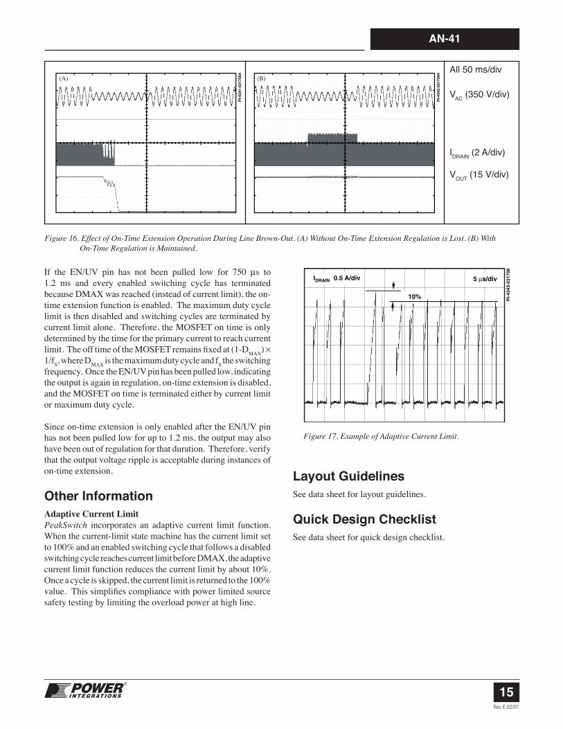
On-Time ExtensionThe on-time extension function of PeakSwitch maximizes the power delivered to the load when the DC input (bulk capacitor) voltage is low. This may allow the use of a smaller input capacitor in designs where the output can droop under peak load, especially in applications where the supply must pass line brown-out or missing AC cycle tests. On-time extension also increases the typical hold-up time.
Figure 16 is an example showing the effect of on-time extension during a line brownout event.
Figure 15. Example of Combined Secondary Over Current and Overvoltage Protection Circuit.
AN-41
Rev. E 02/07
15
Figure 16. Effect of On-Time Extension Operation During Line Brown-Out. (A) Without On-Time Extension Regulation is Lost. (B) With On-Time Regulation is Maintained.
If the EN/UV pin has not been pulled low for 750 µs to 1.2 ms and every enabled switching cycle has terminated because DMAX was reached (instead of current limit), the on-time extension function is enabled. The maximum duty cycle limit is then disabled and switching cycles are terminated by current limit alone. Therefore, the MOSFET on time is only determined by the time for the primary current to reach current limit. The off time of the MOSFET remains fixed at (1-DMAX) × 1/fS, where DMAX is the maximum duty cycle and fS the switching frequency. Once the EN/UV pin has been pulled low, indicating the output is again in regulation, on-time extension is disabled, and the MOSFET on time is terminated either by current limit or maximum duty cycle.
Since on-time extension is only enabled after the EN/UV pin has not been pulled low for up to 1.2 ms, the output may also have been out of regulation for that duration. Therefore, verify that the output voltage ripple is acceptable during instances of on-time extension.
OtherInformationAdaptive Current LimitPeakSwitch incorporates an adaptive current limit function. When the current-limit state machine has the current limit set to 100% and an enabled switching cycle that follows a disabled switching cycle reaches current limit before DMAX, the adaptive current limit function reduces the current limit by about 10%. Once a cycle is skipped, the current limit is returned to the 100% value. This simplifies compliance with power limited source safety testing by limiting the overload power at high line.
All 50 ms/div
VAC (350 V/div)
IDRAIN (2 A/div)
VOUT (15 V/div)
PI-
4341
-031
7064
PI-
4342
-031
7064
Figure 17. Example of Adaptive Current Limit.
(A) (B)
PI-
4343
-031
706
IDRAIN 0.5 A/div 5 µs/div
10%
LayoutGuidelinesSee data sheet for layout guidelines.
QuickDesignChecklistSee data sheet for quick design checklist.

AN-41
Rev. E 02/07
16
Revision Notes DateA - 3/06 B Corrected formatting and text errors. 4/06C Revised device symbol in Figure 1 to be consistent with other PI documentation (added second ground
connection).5/06
D Revised grounding in Figure 1 to match actual implementation. 6/06E Added PKS607. 2/07
For the latest updates, visit our website: www.powerint.comPower Integrations reserves the right to make changes to its products at any time to improve reliability or manufacturability. Power Integrations does not assume any liability arising from the use of any device or circuit described herein. POWER INTEGRATIONS MAKES NO WARRANTY HEREIN AND SPECIFICALLY DISCLAIMS ALL WARRANTIES INCLUDING, WITHOUT LIMITATION, THE IMPLIED WARRANTIES OF MERCHANTABILITY, FITNESS FOR A PARTICULAR PURPOSE, AND NON-INFRINGEMENT OF THIRD PARTY RIGHTS.
PATENTINFORMATION
The products and applications illustrated herein (including transformer construction and circuits external to the products) may be covered by one or more U.S. and foreign patents, or potentially by pending U.S. and foreign patent applications assigned to Power Integrations. A complete list of Power Integrations’ patents may be found at www.powerint.com. Power Integrations grants its customers a license under certain patent rights as set forth at http://www.powerint.com/ip.htm.
LIFESUPPORTPOLICY
POWER INTEGRATIONS’ PRODUCTS ARE NOT AUTHORIZED FOR USE AS CRITICAL COMPONENTS IN LIFE SUPPORT DEVICES OR SYSTEMS WITHOUT THE EXPRESS WRITTEN APPROVAL OF THE PRESIDENT OF POWER INTEGRATIONS. As used herein:
1. A Life support device or system is one which, (i) is intended for surgical implant into the body, or (ii) supports or sustains life, and (iii) whose failure to perform, when properly used in accordance with instructions for use, can be reasonably expected to result in significant injury or death to the user.
2. A critical component is any component of a life support device or system whose failure to perform can be reasonably expected to cause the failure of the life support device or system, or to affect its safety or effectiveness.
The PI logo, TOPSwitch, TinySwitch, LinkSwitch, DPA-Switch, PeakSwitch, Clampless, EcoSmart, E-Shield, Filterfuse, StackFET, PI Expert and PI FACTS are trademarks of Power Integrations, Inc. Other trademarks are property of their respective companies. ©Copyright 2007, Power Integrations, Inc.
PowerIntegrationsWorldwideSalesSupportLocationsWORLD HEADQUARTERS5245 Hellyer AvenueSan Jose, CA 95138, USA.Main: +1-408-414-9200Customer Service: Phone: +1-408-414-9665Fax: +1-408-414-9765e-mail: [email protected]
CHINA (SHANGHAI)Rm 807-808A Pacheer Commercial Centre,555 Nanjing Rd. West Shanghai, P.R.C. 200041Phone: +86-21-6215-5548Fax: +86-21-6215-2468e-mail: [email protected]
CHINA (SHENZHEN)Rm 2206-2207, Block A,Electronics Science & Technology Bldg.2070 Shennan Zhong Rd. Shenzhen, Guangdong,China, 518031Phone: +86-755-8379-3243Fax: +86-755-8379-5828e-mail: [email protected]
GERMANY Rueckertstrasse 3D-80336, Munich GermanyPhone: +49-89-5527-3910Fax: +49-89-5527-3920e-mail: [email protected]
INDIA#1, 14th Main RoadVasanthanagarBangalore-560 052, India Phone: +91-80-4113-8020Fax: +91-80-4113-8023e-mail: [email protected]
ITALYVia De Amicis 2 20091 Bresso MIItalyPhone: +39-028-928-6000Fax: +39-028-928-6009e-mail: [email protected]
JAPAN1st Bldg Shin-Yokohama 2-12-20 Kohoku-ku, Yokohama-shi, Kanagawa ken, Japan 222-0033Phone: +81-45-471-1021Fax: +81-45-471-3717e-mail: [email protected]
KOREARM 602, 6FLKorea City Air Terminal B/D, 159-6Samsung-Dong, Kangnam-Gu,Seoul, 135-728, KoreaPhone: +82-2-2016-6610Fax: +82-2-2016-6630e-mail: [email protected]
SINGAPORE 51 Newton Road#15-08/10 Goldhill PlazaSingapore, 308900Phone: +65-6358-2160Fax: +65-6358-2015e-mail: [email protected]
TAIWAN5F, No. 318, Nei Hu Rd., Sec. 1 Nei Hu Dist.Taipei 114, Taiwan R.O.C.Phone: +886-2-2659-4570Fax: +886-2-2659-4550e-mail: [email protected]
UNITED KINGDOM1st Floor, St. James’s HouseEast Street, FarnhamSurrey GU9 7TJUnited KingdomPhone: +44 (0) 1252-730-140Fax: +44 (0) 1252-727-689 e-mail: [email protected]
APPLICATIONS HOTLINE World Wide +1-408-414-9660
APPLICATIONS FAX World Wide +1-408-414-9760