Embed Size (px)
Citation preview
ARITHMETIC LOGIC UNIT DESIGN FOR SILICON NANOWIRE FIELD-
EFFECT TRANSISTORS LOGIC
NOR HAFIZAH BT MOHD MUNIR ZAHARI
A project report submitted as partial fulfilment of the
requirements for the award of the Master of Engineering
(Electrical-Computer and Microelectronic System)
Faculty of Electrical Engineering
Universiti Teknologi Malaysia
JANUARY 2015

iii
Specially dedicated to my beloved family,
siblings and friends for their
love and sacrifice.

iv
ACKNOWLEDGEMENT
First of all, I would like to take this opportunity to express my gratefulness
for my project supervisor, Dr. Michael Tan Loong Peng for his guidance and
supervision throughout the project period.
Besides, I would like to thank my parents for their support and
encouragement throughout the whole year.
Finally, I would like to show my gratitude for those who has directly and
indirectly in helping me to complete the project.
v
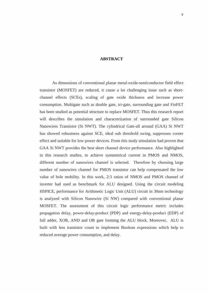
ABSTRACT
As dimensions of conventional planar metal-oxide-semiconductor field effect
transistor (MOSFET) are reduced, it cause a lot challenging issue such as short-
channel effects (SCEs), scaling of gate oxide thickness and increase power
consumption. Multigate such as double gate, tri-gate, surrounding gate and FinFET
has been studied as potential structure to replace MOSFET. Thus this research report
will describes the simulation and characterization of surrounded gate Silicon
Nanowires Transistor (Si NWT). The cylindrical Gate-all around (GAA) Si NWT
has showed robustness against SCE, ideal sub threshold swing, suppresses corner
effect and suitable for low power devices. From this study simulation had proven that
GAA Si NWT provides the best short channel device performance. Also highlighted
in this research studies, to achieve symmetrical current in PMOS and NMOS,
different number of nanowires channel is selected. Therefore by choosing large
number of nanowires channel for PMOS transistor can help compensated the low
value of hole mobility. In this work, 2:3 ratios of NMOS and PMOS channel of
inverter had used as benchmark for ALU designed. Using the circuit modeling
HSPICE, performance for Arithmetic Logic Unit (ALU) circuit in 30nm technology
is analyzed with Silicon Nanowire (Si NW) compared with conventional planar
MOSFET. The assessment of this circuit logic performance metric includes
propagation delay, power-delay-product (PDP) and energy-delay-product (EDP) of
full adder, XOR, AND and OR gate forming the ALU block. Moreover, ALU is
built with less transistor count to implement Boolean expressions which help to
reduced average power consumption, and delay.
vi
ABSTRAK
Pengecillan saiz dimensi Metal-oxide-semiconductor field effect transistor
(MOSFET) menyebabkan banyak isu yang mencabar seperti Short Channel effect
(SCE), scalling of gate oxide thickness dan peningkatan penggunaan kuasa. Antara
alternatif lain bagi mengantikan struktur MOSFET adalah Multigate transistor seperti
double gate, tri-gate, surrounding gate dan FinFET. Melalui laporan penyelidikan ini,
akan menerangkan simulasi dan pencirian Silicon Nanowire Transistor (Si NWT).
Silinder Gate-all around bagi Si NWT menunjukkan pretasi penambah baik terhadap
SCE, sub-threshold swing, corner effect dan sesuai untuk peranti kuasa rendah.
Ditonjolkan juga dalam kajian penyelidikan ini, bagi mencapai semetri arus PMOS
dan NMOS, bilangan saluran nanowires berbeza dipilih bagi menambahan
pengaliran arus. Dalam project ini, 2:3 nisbah NMOS dan PMOS dalam inverter gate
digunakan sebagai rujukaan dalam mengahasilkan ALU litar. Dengan mengunakan
model simulasi HSPICE, prestasi bagi ALU litar dalam teknologi 30nm telah
dianalisi dengan mengunakan Si NW model dan dibandingkan pretasi MOSFET
model sedia ada. Penambah Penuh yang berasaskan Si NW telah menunjukkan
pengurangan yang besar dari segi kelewatan, kuasa yang dilepaskan dan PDP jika
dibandingkan dengan MOSFET dan memberikan kelebihan kepada Si NW dari segi
kecekapan tenaga. Selain itu didalam project ini, pengurangan transistor didalam
ALU litar telah dihasilkan bagi pengahasilan ungkapan Boolean yang tepat bagi
membantu mengurangkan penggunaan kuasa purata, dan kelewatan didalam sebuah
litar ALU.
vii
TABLE OF CONTENTS
CHAPTER TITLE PAGE
DECLARATION ii
DEDICATION iii
ACKNOWLEDGEMENT iv
ABSTRACT v
ABSTRAK vi
TABLE OF CONTENTS vii
LIST OF TABLES x
LIST OF FIGURES xi
LIST OF ABBREVIATIONS xiii
1 INTRODUCTION 1
1.1 Research Background 1
1.2 Problem Statement 4
1.3 Objectives 5
1.4 Research Scope 6
1.5 Contribution 6
1.6 Thesis Outline 7
2 LITERATURE REVIEW 8
2.1 Introduction to MOSFET 8
2.2 Shrinking Technology of MOSFET 9
2.3 Short Channel Effect 11
2.4 Threshold Voltage Roll-Off 12
2.5 Drain Induced Barrier Lowering (DIBL) 13
2.6 Silicon Nanowire FET (SNWFET) 15
viii
2.6.1 Nanowire FET Structure and
Performance Benefit
15
2.6.2 Limitation of GAA Nanowire FET 18
2.6.3 Silicon Nanowire FET for Logic
Transistor Application
18
2.7 Arithmetic Operation 19
2.7.1 Full Adder Design 20
2.7.2 Ripple Carry Adder Design 21
2.7.3 Carry-Look Ahead Adder Design 21
2.8 Digital Circuit Style 23
2.8.1 CMOS AND GATE and OR Gate 23
2.8.2 CMOS XOR GATE 24
2.8.3 Full Adder Cell 27
3 RESERCH METHODOLOGY 30
3.1 Introduction 30
3.2 BSIM-CMG Model for GAA Si NW 33
3.3 HSPICE Simulator 34
3.4 CosmosScope 35
3.5 MATLAB Simulator 36
4 RESULTS AND DISCUSSION 37
4.1 Introduction 37
4.2 Structure GAA Si NW 38
4.3 Current-Voltage Relationship of P-type and N-
type Si NW
39
4.4 4 Bit ALU Design and Operation 42
4.4.1 Multiplexer Design 44
4.4.2 Combinational Logic and Adder Design 46
4.5 Propagation Delay 48
4.6 Average Power Dissipation 49
4.7 Power-Delay-Product (PDP) and Energy-
Delay-Product (EDP)
51
ix
5 PROJECT MANAGEMENT 54
5.1 Introduction 54
5.2 Project Schedule 54
6 CONCLUSION AND FUTURE WORK 57
6.1 Conclusion 57
6.2 Problem and Limitation 58
6.3 Future Work 59
REFERENCES 60
x
LIST OF TABLES
TABLE NO. TITLE PAGE
2.1 The year of introduction and the number of transistor
on the processors of Intel Corporation [5]
10
2.2 Result of Comparison between TSNWFET vs FinFET
[35]
19
4.1 Parameter value that have been used in Si NW model 38
4.2 Result Vth, Current Ratio, DIBL and SS for Si NW
channel Ratio 2:3 (NMOS:PMOS) of inverter
42
4.3 Truth Table of a 2 to 1 multiplexer 46
4.4 Propagation Delay of GAA Si NWT and MOSFET
base ALU
49
4.5 Average power dissipation of Si NW and MOSFET-
based ALU
50
4.6 Power-Delay-Product (PDP) of Si NWT and
MOSFET ALU
51
4.7 Energy-Delay-Product (EDP) of Si NWT and
MOSFET ALU
52
5.1 Project Gantt chart of Semester 1/2013 55
5.2 Project Gantt chart of Semester 2/2014 56
6.1 The Advantage of Si NWT with reduction on transistor
count and comparison with conventional MOSFET
based.
58
xi
LIST OF FIGURES
FIGURE NO. TITLE PAGE
1.1 Scaling of transistor size (physical gate length) with
technology node to sustain Moore’s Law. Nodes
with feature size less than 100 nm can be referred to
as nanotechnology. [1]
2
1.2 Next generation of extended Moore Law's [1] 3
1.3 Intel’s future development plan showing a trend in
size reduction [8]
4
2.1 Schematic of MOSFET [11] 9
2.2 MOSFET Gate Length reduces with the Technology
Generation [22]
10
2.3 The ID-VG characteristics for the studied device
with on-state current and threshold voltage [22]
12
2.4 Surface potential of Device β for 0.1 V and 1.5 V
drain voltages (linear and saturated case) [24].
13
2.5 Example of a drain-induced barrier-lowering (DIBL)
from ID-VGS curves [22]
14
xii
2.6 (a) 60nm-wide channel of Silicon Nanowire
Transistor designed. Silicon is used as the material
of channel that connects the source and drain region
of a transistor [31]. (b) The structure of Gate-All-
Around (GAA) Twin Silicon Nanowire FET
fabricated [29].
16
2.7 (a) geometry of a planar bulk MOSFET and (b)
geometry of a NWFET device [32]
17
2.8 4bit ripple carry adder (RCA) [37] 21
2.9 4bit Carry Lookahead Adder (CLA) [37] 22
2.10 (a) AND Gate of CMOS NAND gate cascade in
series with a CMOS inverter (b) OR gate of CMOS
NOR gate cascade in series with CMOS inverter
24
2.11 XOR Gate using pass transistor [41] 25
2.12 Topology of an and-or-invert-21 (AOI-21) gate [42] 26
2.13 XOR gate using 2-1 AOI gate and NOR gate 27
2.14 Conventional CMOS full adder [43] 28
2.15 9T Transistor using XNOR gate architecture [44] 29
3.1 Simulation Tool used throughout the Research
Project
31
3.2 Research Work flow
32
xiii
3.3 The different multi-gate FINFETs that can be
simulated by BSIM-CMG. BULKMOD is selected
for substrate (SOI or bulk) and ASYMMOD enable
is for an asymmetric I-V [49]
33
3.4 HSPICE user interface simulator 34
3.5 (a) Netlist .sp file for HSPICE input. (b) Listing
file .lis for measurement result
35
4.1 Schematic diagrams of Cylindrical GAA Si NWT 38
4.2 Multi-fin of multigate FET layout (a) show the
NFIN=2 NF=1 for TSNWFET (b) show the NFIN=1
and NF=1 for Si NW.
39
4.3 I-V characteristic Id vs Vg for different number of
channel.
40
4.4 (a) ID-VG characteristic of N- and PMOS transistor
connected in inverter LG=30nm (b) ID-VD
characteristic N- and PMOS transistor connected in
Inverter circuit LG=30nm
40
4.5 (a) Example of IDS versus VGS Curve in log 10
scale (a) N-Si NW type IV curves (b) P-Si NW type
IV curves
41
4.6 Schematic ALU circuit proposed for project 43
4.7 1 Bit ALU Design circuit level 44
4.8 Block diagram of multiplexer logic at output stage 45
xiv
4.9 Circuit diagram of 2 to 1 multiplexer design.
45
4.10 Circuit diagram for Arithmetic logic and
combinational logic design (a) AND gate (Y10=AB)
(b) OR gate (Y00 =A+B) (c) XOR gate (Y11=AxorB)
(d) Adder (Ysum=A xor Cin , Cout= A and B + Cin (A
xor B).
47
4.11 Waveform output from CosmosScope of the 1 bit
ALU
48
4.12 Average power dissipation of Si NW and MOSFET-
based ALU
50
4.13 The power delay product (PDP) of (a) MOSFET and
(b) Si NWT based ALU
52
4.14 The energy-delay-product (EDP) of Si NWT as
compared with MOSFET based ALU.
53
xv
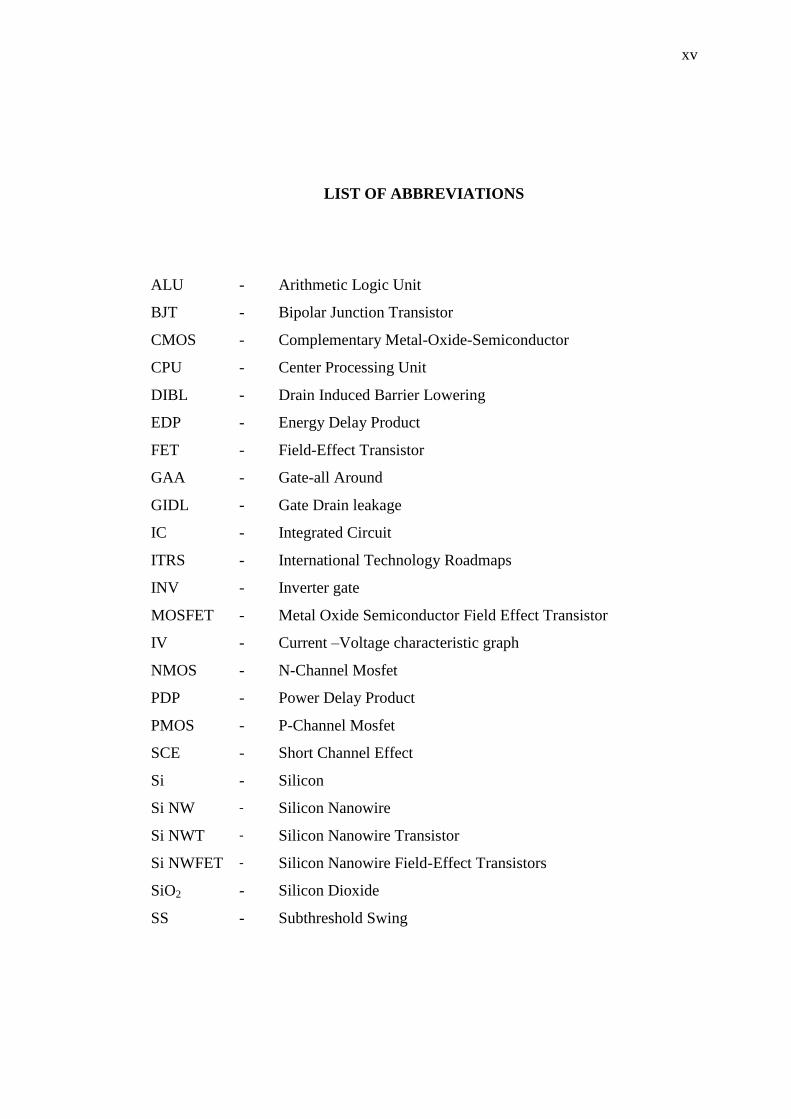
LIST OF ABBREVIATIONS
ALU - Arithmetic Logic Unit
BJT - Bipolar Junction Transistor
CMOS - Complementary Metal-Oxide-Semiconductor
CPU - Center Processing Unit
DIBL - Drain Induced Barrier Lowering
EDP - Energy Delay Product
FET - Field-Effect Transistor
GAA - Gate-all Around
GIDL - Gate Drain leakage
IC - Integrated Circuit
ITRS - International Technology Roadmaps
INV - Inverter gate
MOSFET - Metal Oxide Semiconductor Field Effect Transistor
IV - Current –Voltage characteristic graph
NMOS - N-Channel Mosfet
PDP - Power Delay Product
PMOS - P-Channel Mosfet
SCE - Short Channel Effect
Si - Silicon
Si NW - Silicon Nanowire
Si NWT - Silicon Nanowire Transistor
Si NWFET - Silicon Nanowire Field-Effect Transistors
SiO2 - Silicon Dioxide
SS - Subthreshold Swing
CHAPTER 1
INTRODUCTION
1.1 Research Background
Integrated Circuit (IC) technology has been observed as one of the most
important inventions in engineering history. With an incredible progress in IC
technology since 1971, there were about 2,300 transistors with a size of 10
micrometres (10,000 nanometres) on a 12 square millimetres chip. Till today, the 3rd
generation Intel Corei7 has 1.4 billion transistors with the size of 22 nanometres, on
a 160 square millimetres chip.
With reduction of transistors sizes, more things could be built on a chip and it
can increases the processing power of the center processing unit (CPU) by having
more processor cores with higher clock frequency and more data cache space. As a
result the processor could run faster on more than one thing at the same time, and
could store more information.
Thus with a new trend in IC technology, Moore’s Law today is not showing
any sign of slowing down, but they are showing signs of changing by looking
consideration on scaling down the dimension of each transistor in the basic element
of integrated circuits and the increasing the total numbers of transistors in one chip.
2
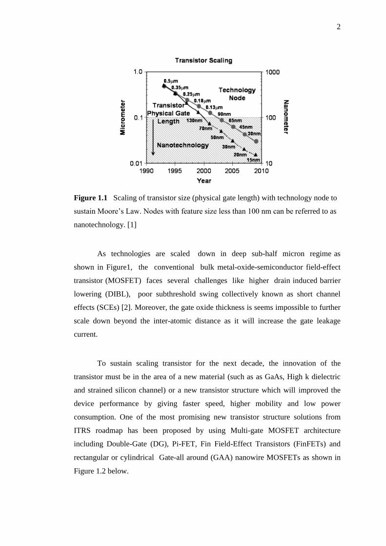
Figure 1.1 Scaling of transistor size (physical gate length) with technology node to
sustain Moore’s Law. Nodes with feature size less than 100 nm can be referred to as
nanotechnology. [1]
As technologies are scaled down in deep sub-half micron regime as
shown in Figure1, the conventional bulk metal-oxide-semiconductor field-effect
transistor (MOSFET) faces several challenges like higher drain induced barrier
lowering (DIBL), poor subthreshold swing collectively known as short channel
effects (SCEs) [2]. Moreover, the gate oxide thickness is seems impossible to further
scale down beyond the inter-atomic distance as it will increase the gate leakage
current.
To sustain scaling transistor for the next decade, the innovation of the
transistor must be in the area of a new material (such as as GaAs, High k dielectric
and strained silicon channel) or a new transistor structure which will improved the
device performance by giving faster speed, higher mobility and low power
consumption. One of the most promising new transistor structure solutions from
ITRS roadmap has been proposed by using Multi-gate MOSFET architecture
including Double-Gate (DG), Pi-FET, Fin Field-Effect Transistors (FinFETs) and
rectangular or cylindrical Gate-all around (GAA) nanowire MOSFETs as shown in
Figure 1.2 below.
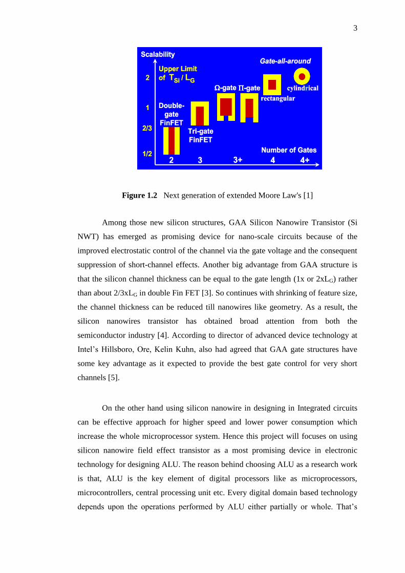
3
Figure 1.2 Next generation of extended Moore Law's [1]
Among those new silicon structures, GAA Silicon Nanowire Transistor (Si
NWT) has emerged as promising device for nano-scale circuits because of the
improved electrostatic control of the channel via the gate voltage and the consequent
suppression of short-channel effects. Another big advantage from GAA structure is
that the silicon channel thickness can be equal to the gate length (1x or 2xLG) rather
than about 2/3xLG in double Fin FET [3]. So continues with shrinking of feature size,
the channel thickness can be reduced till nanowires like geometry. As a result, the
silicon nanowires transistor has obtained broad attention from both the
semiconductor industry [4]. According to director of advanced device technology at
Intel’s Hillsboro, Ore, Kelin Kuhn, also had agreed that GAA gate structures have
some key advantage as it expected to provide the best gate control for very short
channels [5].
On the other hand using silicon nanowire in designing in Integrated circuits
can be effective approach for higher speed and lower power consumption which
increase the whole microprocessor system. Hence this project will focuses on using
silicon nanowire field effect transistor as a most promising device in electronic
technology for designing ALU. The reason behind choosing ALU as a research work
is that, ALU is the key element of digital processors like as microprocessors,
microcontrollers, central processing unit etc. Every digital domain based technology
depends upon the operations performed by ALU either partially or whole. That’s
4
why it highly required designing high speed ALU, which can enhance the efficiency
of those modules which lies upon the operations performed by ALU [6].
1.2 Problem Statements
The breaking down of Moore’s law has been predicted the dead end since
2010 as computer power simply cannot maintain its rapid exponential rise using
standard silicon technology. The downscaling of the feature size in CMOS
technology had made conventional CMOS transistor model is facing severe
challenges for scaling beyond 22nm nodes [7].
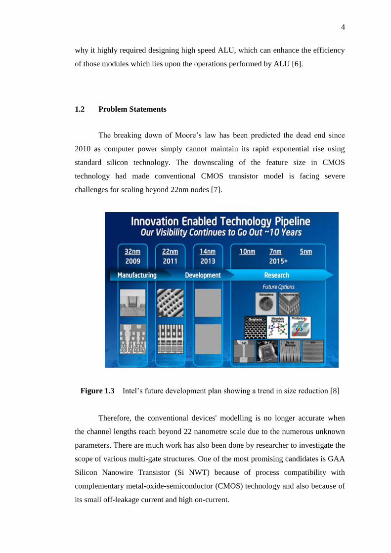
Figure 1.3 Intel’s future development plan showing a trend in size reduction [8]
Therefore, the conventional devices' modelling is no longer accurate when
the channel lengths reach beyond 22 nanometre scale due to the numerous unknown
parameters. There are much work has also been done by researcher to investigate the
scope of various multi-gate structures. One of the most promising candidates is GAA
Silicon Nanowire Transistor (Si NWT) because of process compatibility with
complementary metal-oxide-semiconductor (CMOS) technology and also because of
its small off-leakage current and high on-current.
5
On the other hand, nowadays ALU design in digital IC that has low power
consumption, high speed and energy efficient is in highly demand. As a result the use
of convention transistor i.e. MOSFET in ALU circuit design has also spotted
reaching it performance limit such as average power dissipation and speed as the
sizes reaches nanometres scale. One of new structure alternative to solve the problem
proposed by Technology Roadmap of Semiconductor (ITRS) is Si nanowires FET to
replace conventional transistor MOSFET.
Therefore in this project, the performance if GAA Si NWT in digital system
namely ALU circuit is explorer. This can be achieved by investigating the physical
of Silicon nanowires as compared with MOSFET. Hence the problems in this project
are:
1. How does the performance of silicon Nanowires Field effect on Bulk wafer?
2. How Gate-All-Around Si NW characteristic design for CMOS Inverter?
3. What is the maximum number of Si NW channel can be replaced to obtain
the optimum performance of the device?
4. What are the performance differences in logic circuit such as ALU using
GAA Si NWT as compared with MOSFET
1.3 Objectives
The project focuses on to develop and analysed the GAA Silicon Nanowire
(NW) vs traditional convention MOSFET which is based on 30nm process
technology. Thus the objectives of this project are:
1. To build circuit and simulate using HSPICE based on GAA Si NWT.
2. To obtain symmetrical output IV characteristic GAA Si NWT with
number of channel variation between N and P type.
3. To optimize the ALU circuit with the smaller number of transistor
count.
6
Research Scope 1.4
There are few research scopes that are highlighted in this project. This
research scope cover analysed and developed the Cylindrical Si NWT (GAA) and
MOSFET which is based on 30nm process technology. First, the Si NWT
characteristic is obtained from IV curve with different number of channel N and P
type by choosing CMOS inverter as the test vehicle. The transistor model that been
use through this project is from BSIM-CMG model. Once the drive current for N and
PMOS transistor are matched using different number of channel for each and
excellent performance of the inverter is achieved from GAA Si NWT model, then the
ALU circuit is applied in SPICE code where the code will be simulated in HSPICE
and the graph will be plotted in CosmoScope and Matlab. This project will analyse
on performance of Si NWT ALU using 30nm Berkeley Short-channel IGFET Model-
Common Multi-Gate (BSIM CMG) model against 30nm conventional MOSFET
model. The important metric performances such as power delay product (PDP) and
energy delay product (EDP) will be obtained.
Contribution 1.5
GAA Si NWT structure is a new alternative solution for conventional
MOSFET as identified by The International Technology Roadmap for
Semiconductor (ITRS), would give great advantages over the conventional CMOS.
This project successfully reveals few items as show below:
1. Achieved different number of channel for each N and P type of Si NW in
logic gate. A symmetry in NMOS and PMOS current is achieved by using 2
channel wire N-type and 3 channel wires for Ptype of GAA nanowires
CMOS inverters as benchmark.
2. Design the ALU using ripple carrier adder (RCA) structure with 2-1
multiplexer connected in parallel in order to maintain the speed of the circuit.
Optimize the transistor count in the logic gate to improve the performance by
using 2-1 AND-OR-Invert Logic (AOI) Gate and one NOR without any INV.
3. Achieved better performance ALU with Si NW as compare to Benchmark
MOSFET in propagation delay, power and efficiency of the circuit.
7
Thesis Outline 1.6
This Project consists of five chapters. The first chapter provides an
introduction to this research including the objective and fields of study. The theories
and fundamental about relevant research are discussed in the second chapter.
Additional information related to this project are taking from journal or other
research as references to understand the physical silicon nanowire transistor and
manufacturing process. Apart from that, the results from other research thesis, User's
Manual and datasheet are obtained. In the third chapter, research and method are
recorded and explained in details can be explained in detail. Chapter 4 will provide
the conclusion and the future work can be expand in the project.
REFERENCES
1. Chau, R., Datta, S., Doczy, M., Doyle, B., Jin, B., Kavalieros, J., &
Radosavljevic, M. (2005). Benchmarking nanotechnology for high-
performance and low-power logic transistor applications. Nanotechnology,
IEEE Transactions on, 4(2), 153-158.
2. E. J. Nowak, I. Aller, T. Ludwig, K. Kim, R. V. Joshi, C.-T. Chuang, K.
Bernstein, and R. Puri,“Turning silicon on its edge [double gate
CMOS/FinFET technology],” IEEE Circuits Devices Mag., vol. 20, no.1,
pp. 20–31, Jan. /Feb. 2004.
3. Huang, R., Wang, R., Zhuge, J., Liu, C., Yu, T., Zhang, L., & Wang, Y.
(2011, September). Characterization and analysis of gate-all-around Si
nanowire transistors for extreme scaling. In Custom Integrated Circuits
Conference (CICC), 2011 IEEE (pp. 1-8). IEEE.
4. Vaddi, R., Agarwal, R. P., Dasgupta, S., & Kim, T. T. (2011). Design and
Analysis of Double-Gate MOSFETs for Ultra-Low Power Radio Frequency
Identification (RFID): Device and Circuit Co-Design. Journal of Low Power
Electronics and Applications, 1(2), 277-302.
5. WEBSITE: http://spectrum.ieee.org/semiconductors/devices/nanowire-
transistors-could-keep-moores-law-alive Retrieved Apr 29, 2013
6. Gupta, M. A., Malviya, M. U., & Kapse, V. A Novel Approach to Design
High Speed Arithmetic Logic Unit Based On Ancient Vedic Multiplication
Technique.
7. WEBSITE: http://technologicallyinsane.wordpress.com/tag/moores-law/
Retrieved April 5, 2013
8. Dunga, M. V. (2008). Nanoscale CMOS modeling. ProQuest.
9. D. Kahng and M. M. Atalla, “Silicon-silicon dioxide field induced surface
device,”Proc. IRE-AIEE Solid-State Device Res. Conf. Pittsburgh, PA,1960.
10. Rabaey J. M., Chandrakasan A. P., Nikolic B. Digital integrated circuits, vol.
[3]
11. Tunneling field effect transistors: beyond moore’s law, Prentice hall
Englewood Cliffs. 2002. [http://berc.berkeley.edu/tunneling-field-effect-
transistors-beyond-moores-law/]
12. International Technology Roadmap for Semiconductor (ITRS) - updated
[www.itrs.net/Links/2006update/2006updatefinal.htm]
13. G. Moore, “Progress in digital integrated electronics,” IEEE International
Electron.Dev. Meeting (IEDM) Tech. Digest, pp. 11-13, 1975.
14. Website:http://www.intel.com/pressroom/kits/events/moores_law_40th/?iid=t
ech_mooreslaw+body_presskit Retrieved
15. “International Technology Roadmap for Semiconductors.” 2008 Edition
available online at http://public.itrs.net/
61
16. H.Wakabayashi,T. Ezaki, M Hane, S. Yamagami, N.
IkarasK.Takeuchi,T.Yamamoto, T. Mogami, T. Ikezawa, T. Sakamoto, H.
Kawaura,“Transport properties of sub-10-nm planar-bulk-CMOS devices,”
IEEE Int. Electron Dev. Meeting Tech. Dig., p. 429, Dec 2004.
17. Chaudhry, A., & Kumar, M. J. (2004). Controlling short-channel effects in
deep-submicron SOI MOSFETs for improved reliability: a review. Device
and Materials Reliability, IEEE Transactions on, 4(1), 99-109.
18. D‟Agostino, F. and D. Quercia (2000)."Short-channel effects in MOSFETs."
University College London: 1-15.
19. Davari, B., et al. (1995). "CMOS scaling for high performance and low
powerthe next ten years." Proceedings of the IEEE 83(4): 595-606.
20. D‟Agostino,F. and D. Quercia (2000)."Short-channel effects in MOSFETs."
University College London: 1-15.
21. Davari, B., et al. (1995). "CMOS scaling for high performance and low
powerthe next ten years." Proceedings of the IEEE 83(4): 595-606.
22. Li, Y., & Hwang, C. H. (2009). DC baseband and high-frequency
characteristics of a silicon nanowire field effect transistor
circuit. Semiconductor Science and Technology, 24(4), 045004.
23. R. R. Troutman, “VLSI limitation from drain-induced barrier lowering,”
IEEETrans. Electron Devices, vol. ED-26, pp. 461–469, April 1979.
24. Chaudhry, A., & Kumar, M. J. (2004). Controlling short-channel effects in
deep-submicron SOI MOSFETs for improved reliability: a review. Device
and Materials Reliability, IEEE Transactions on, 4(1), 99-109.
25. WEBSITE:http://www.ece.unm.edu/~jimp/vlsi_test/slides/html/iddq1.html.
Retrieved Disember 14, 2013.
26. Suk, S. D., Lee, S. Y., Kim, S. M., Yoon, E. J., Kim, M. S., Li, M., ... & Ryu,
B. I. (2005, December). High performance 5nm radius Twin Silicon
Nanowire MOSFET (TSNWFET): fabrication on bulk si wafer,
characteristics, and reliability. In Electron Devices Meeting, 2005. IEDM
Technical Digest. IEEE International (pp. 717-720). IEEE.
27. Suk, S. D., Yeo, K. H., Cho, K. H., Li, M., Yeoh, Y. Y., Lee, S. Y., ... & Park,
D. (2008). High-performance twin silicon nanowire MOSFET (TSNWFET)
on bulk Si wafer. Nanotechnology, IEEE Transactions on, 7(2), 181-184.
28. [28] Koo, S. M., Edelstein, M. D., Li, Q., Richter, C. A., & Vogel, E. M.
(2005). Silicon nanowires as enhancement-mode Schottky barrier field-effect
transistors. Nanotechnology, 16(9), 1482.
29. Suk, S. D., Li, M., Yeoh, Y. Y., Yeo, K. H., Cho, K. H., Ku, I. K., ... & Lee,
W. S. (2007, December). Investigation of nanowire size dependency on
TSNWFET. In Electron Devices Meeting, 2007. IEDM 2007. IEEE
International(pp. 891-894). IEEE.
30. Pott, V., Moselund, K. E., Bouvet, D., De Michielis, L., & Ionescu, A. M.
(2008). Fabrication and characterization of gate-all-around silicon nanowires
on bulk silicon. Nanotechnology, IEEE Transactions on, 7(6), 733-744.
31. [Appenzeller, J., Knoch, J., Bjork, M. T., Riel, H., Schmid, H., & Riess, W.
(2008). Toward nanowire electronics. Electron Devices, IEEE Transactions
on,55(11), 2827-2845.
32. Rahman, M. M. (2011). Fabrication and Characterization of High
Performance Silicon Nanowire Field Effect Transistors.
33. Barraud, S., Coquand, R., Casse, M., Koyama, M., Hartmann, J., Maffini-
Alvaro, V., & Poiroux, T. (2012). Performance of omega-shaped-gate silicon
62
nanowire MOSFET with diameter down to 8 nm. Electron Device Letters,
IEEE,33(11), 1526-1528.
34. Chau, R., Datta, S., Doczy, M., Doyle, B., Jin, B., Kavalieros, J., ... &
Radosavljevic, M. (2005). Benchmarking nanotechnology for high-
performance and low-power logic transistor applications. Nanotechnology,
IEEE Transactions on, 4(2), 153-158.
35. Amarú, L., Gaillardon, P. E., & De Micheli, G. (2013). Efficient Arithmetic
Logic Gates Using Double-Gate Silicon Nanowire FETs. In 2013 Ieee 11Th
International New Circuits And Systems Conference (Newcas) (No. EPFL-
CONF-195306). Ieee.
36. Kumar, R., & Dahiya, S [2013]. Performance Analysis of Different Bit Carry
Look Ahead Adder Using VHDL Environment. International Journal of
Engineering Science and Innovative Technology (IJESIT) Volume, 2.
37. Rabaey, J. M., Chandrakasan, A. P., & Nikolic?, B. (2003). Digital integrated
circuits: A design perspective. Upper Saddle River, N.J: Pearson Education.
38. Kumar, J., & Kaur, P. (2013). Comparative Performance Analysis of
Different CMOS Adders Using 90nm and 180nm
Technology. technology, 2(8).
39. Uma, R., Vijayan, V., Mohanapriya, M., & Paul, S. (2012). Area, Delay and
Power Comparison of Adder Topologies. International Journal of VLSI and
Communication Systems, 254.
40. Naraghi, S. (2004). Reduced swing Domino techniques for low power and
high performance arithmetic circuits (Doctoral dissertation, University of
Waterloo).
41. Zimmermann, R., & Fichtner, W. (1997). Low-power logic styles: CMOS
versus pass-transistor logic. IEEE Journal of Solid-state Circuits.
doi:10.1109/4.597298
42. Wolf, Wayne. Modern VLSI Design: System-onchip Design. Upper Saddle
River, NJ: Prentice Hall PTR, 2002. Print
43. Hiremath, Y., Kulkarni, A. L., & Baligar, J. S. Design and Implementation of
Ripple Carry Adder using area efficient full adder cell in 180nm CMOS
Technology.
44. Tripti Sharma (2012). Low Power 1-Bit 9T Full Adder Cell using XNOR
Logic. doi:10.3850/978-981-07-1403-1_225
45. Valinajad, H., Hosseini, R., & Akbari (2012), M. E. Electrical Characteristics
Of Strained Double Gate Mosfet.
46. Chaudhry, A., & Kumar, M. J. (2004). Controlling short-channel effects in
deep-submicron SOI MOSFETs for improved reliability: a review. Device
and Materials Reability, IEEE Transction on, 4(1), 99-109.
47. Lu, D. D. (2011). Compact models for future generation CMOS.
48. Chauhan, Y. S., Lu, D. D., Venugopalan, S., Karim, M. A., Niknejad, A., &
Hu, C. (2011). Compact models for sub-22 nm MOSFETs. In Proc.
Workshop Compact Model.
49. Paydavosi, N. A. V. I. D., Venugopalan, S. R. I. R. A. M. K. U. M. A. R.,
Chauhan, Y. S., Duarte, J. P., Jandhyala, S., Niknejad, A. M., & Hu, C. C.
(2013). BSIM—SPICE models enable FinFET and UTB IC designs. Access,
IEEE, 1, 201-215.
50. Compton, K. (n.d.). Carry Lookahead Adders. Retrieved December 24, 2013,
from http://pages.cs.wisc.edu/~jsong/CS352/Readings/CLAs.pdf
63
51. Yeo, K. H., Suk, S. D., Li, M., Yeoh, Y. Y., Cho, K. H., Hong, K. H., ... &
Ryu, B. I. (2006). Gate-all-around (GAA) twin silicon nanowire MOSFET
(TSNWFET) with 15 nm length gate and 4 nm radius nanowires. In 2006
International Electron Devices Meeting (pp. 1-4).
52. Suk, S. D., Lee, S. Y., Kim, S. M., Yoon, E. J., Kim, M. S., Li, M., ... & Ryu,
B. I. (2005, December). High performance 5nm radius Twin Silicon
Nanowire MOSFET (TSNWFET): fabrication on bulk si wafer,
characteristics, and reliability. In Electron Devices Meeting, 2005. IEDM
Technical Digest. IEEE International (pp. 717-720). IEEE.
53. Kim, D.W., et al. (2008). Twin Silicon Nanowire FET (TSNWFET) On SOI
With 8 nm Silicon Nanowires and 25 nm Surrounding TiN Gate. Suk, S.D.
High Performance 5nm radius Twin Silicon Nanowire
MOSFET(TSNWFET) : Fabrication on Bulk Si Wafer, Characteristics, and
Reliability
54. Yang, F. L., Lee, D. H., Chen, H. Y., Chang, C. Y., Liu, S. D., Huang, C.
C., ... & Hu, C. (2004, June). 5nm-gate nanowire FinFET. In VLSI
Technology, 2004. Digest of Technical Papers. 2004 Symposium on (pp. 196-
197). IEEE.
55. Buddharaju, K. D., Singh, N., Rustagi, S. C., Teo, S. H., Wong, L. Y., Tang,
L. J., & Kwong, D. L. (2007, September). Gate-all-around Si-nanowire
CMOS inverter logic fabricated using top-down approach. In Solid State
Device Research Conference, 2007. ESSDERC 2007. 37th European (pp.
303-306). IEEE.
56. Bangsaruntip, S., Cohen, G. M., Majumdar, A., Zhang, Y., Engelmann, S. U.,
Fuller, N. C. M., & Sleight, J. W. (2009, December). High performance and
highly uniform gate-all-around silicon nanowire MOSFETs with wire size
dependent scaling. In Electron Devices Meeting (IEDM), 2009 IEEE
International (pp. 1-4). IEEE.
57. Singh, N., Buddharaju, K. D., Manhas, S. K., Agarwal, A., Rustagi, S. C., Lo,
G. Q., ... & Kwong, D. L. (2008). Si, SiGe nanowire devices by top–down
technology and their applications. Electron Devices, IEEE Transactions
on,55(11), 3107-3118.
58. Ranganathan, N., Kougianos, E., & Patra, P. (2008). Low-power high-level
synthesis for nanoscale CMOS circuits (Vol. 387764739). New York, NY:
Springer.
59. Compton, K. (n.d.). Carry Lookahead Adders. Retrieved December 24, 2013,
from http://pages.cs.wisc.edu/~jsong/CS352/Readings/CLAs.pdf