Embed Size (px)
Citation preview
1
AT45DB081D and AT45DB081E
Comparison
Adesto Field Application
http://www.adestotech.com/
2
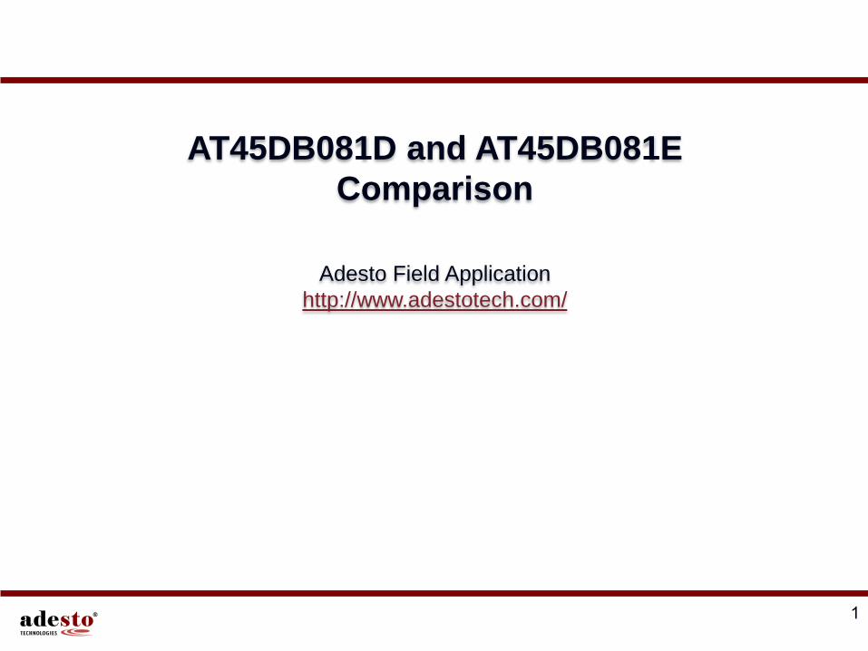
Content:
Differences Highlight – require software change
Features Highlight for AT45DB081E
Features not recommended for new design
AT45DB081E Command Set Summary
Program / Erase Time comparison
Feature description
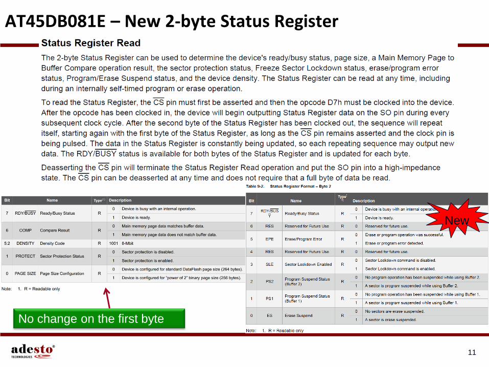
2-byte Status Register
Enter and exit Ultra-Deep Power Down
Freeze Sector Lockdown
Buffer and Page size reconfiguration
Software Reset
Low Power Read Mode
Program / Erase Suspend and Resume
AT45DB081D and AT45DB081E Comparison
3
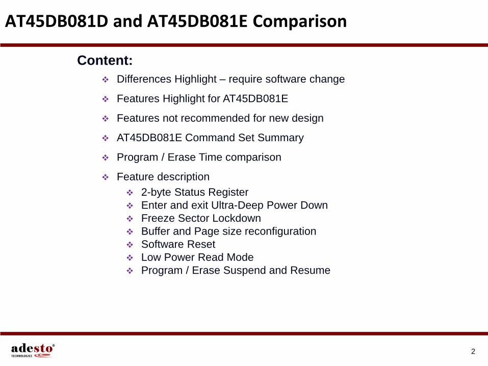
Command: No change
Product ID: No change
Page Program Time: Change from 35msec to 40msec
Status Register: No change
AT45DB081E Differences Highlight – Items require Software Change
Conversion from AT45DB081D to AT45DB081E
4
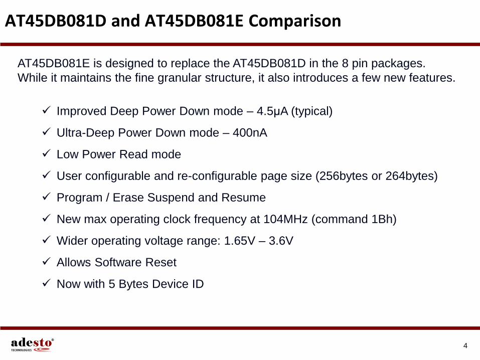
AT45DB081E is designed to replace the AT45DB081D in the 8 pin packages.
While it maintains the fine granular structure, it also introduces a few new features.
Improved Deep Power Down mode – 4.5μA (typical)
Ultra-Deep Power Down mode – 400nA
Low Power Read mode
User configurable and re-configurable page size (256bytes or 264bytes)
Program / Erase Suspend and Resume
New max operating clock frequency at 104MHz (command 1Bh)
Wider operating voltage range: 1.65V – 3.6V
Allows Software Reset
Now with 5 Bytes Device ID
AT45DB081D and AT45DB081E Comparison
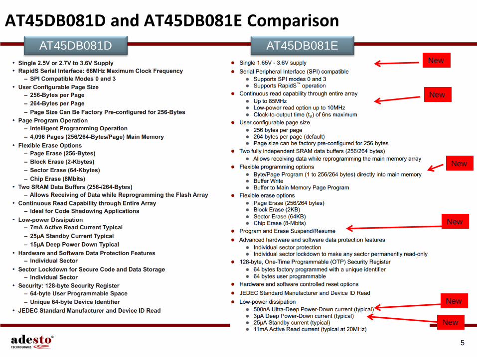
5
New
New
New
New
New
AT45DB081D AT45DB081E
New
AT45DB081D and AT45DB081E Comparison
6
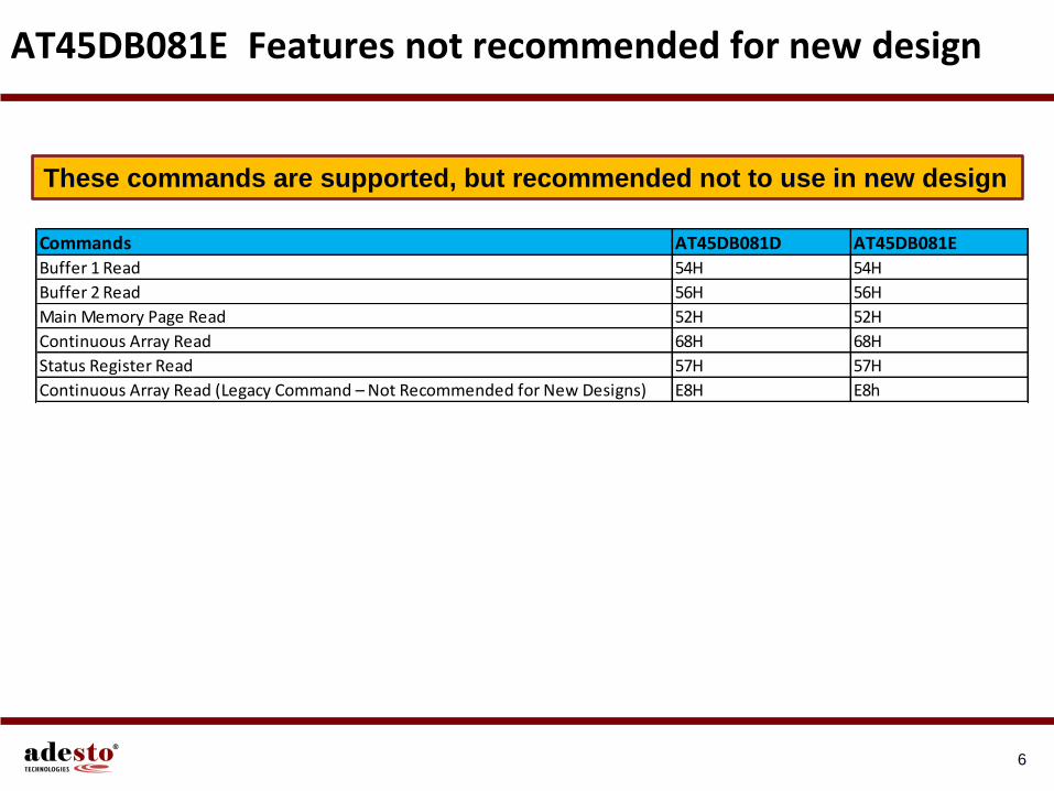
These commands are supported, but recommended not to use in new design
Commands AT45DB081D AT45DB081E
Buffer 1 Read 54H 54H
Buffer 2 Read 56H 56H
Main Memory Page Read 52H 52H
Continuous Array Read 68H 68H
Status Register Read 57H 57H
Continuous Array Read (Legacy Command – Not Recommended for New Designs) E8H E8h
AT45DB081E Features not recommended for new design
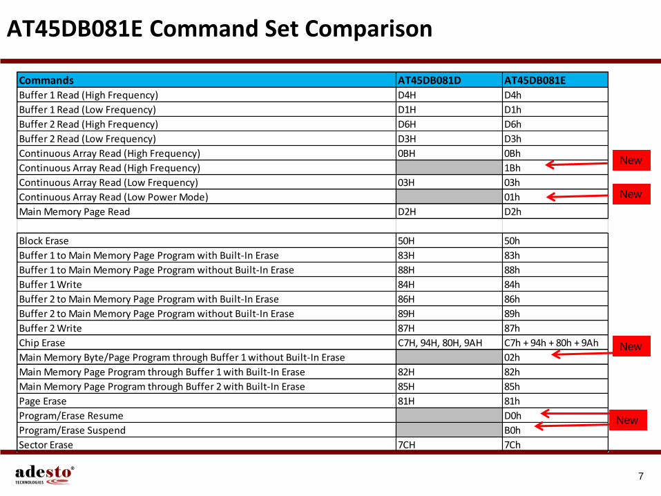
Commands AT45DB081D AT45DB081EBuffer 1 Read (High Frequency) D4H D4h
Buffer 1 Read (Low Frequency) D1H D1h
Buffer 2 Read (High Frequency) D6H D6h
Buffer 2 Read (Low Frequency) D3H D3h
Continuous Array Read (High Frequency) 0BH 0Bh
Continuous Array Read (High Frequency) 1Bh
Continuous Array Read (Low Frequency) 03H 03h
Continuous Array Read (Low Power Mode) 01h
Main Memory Page Read D2H D2h
Block Erase 50H 50h
Buffer 1 to Main Memory Page Program with Built-In Erase 83H 83h
Buffer 1 to Main Memory Page Program without Built-In Erase 88H 88h
Buffer 1 Write 84H 84h
Buffer 2 to Main Memory Page Program with Built-In Erase 86H 86h
Buffer 2 to Main Memory Page Program without Built-In Erase 89H 89h
Buffer 2 Write 87H 87h
Chip Erase C7H, 94H, 80H, 9AH C7h + 94h + 80h + 9Ah
Main Memory Byte/Page Program through Buffer 1 without Built-In Erase 02h
Main Memory Page Program through Buffer 1 with Built-In Erase 82H 82h
Main Memory Page Program through Buffer 2 with Built-In Erase 85H 85h
Page Erase 81H 81h
Program/Erase Resume D0h
Program/Erase Suspend B0h
Sector Erase 7CH 7Ch
7
New
New
New
New
AT45DB081E Command Set Comparison
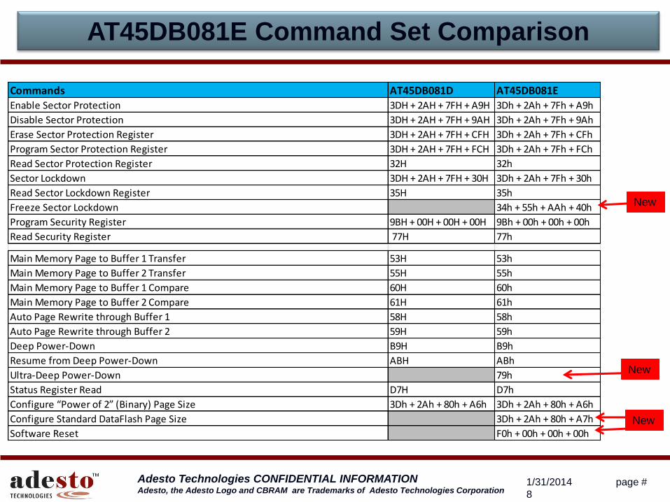
Commands AT45DB081D AT45DB081EEnable Sector Protection 3DH + 2AH + 7FH + A9H 3Dh + 2Ah + 7Fh + A9h
Disable Sector Protection 3DH + 2AH + 7FH + 9AH 3Dh + 2Ah + 7Fh + 9Ah
Erase Sector Protection Register 3DH + 2AH + 7FH + CFH 3Dh + 2Ah + 7Fh + CFh
Program Sector Protection Register 3DH + 2AH + 7FH + FCH 3Dh + 2Ah + 7Fh + FCh
Read Sector Protection Register 32H 32h
Sector Lockdown 3DH + 2AH + 7FH + 30H 3Dh + 2Ah + 7Fh + 30h
Read Sector Lockdown Register 35H 35h
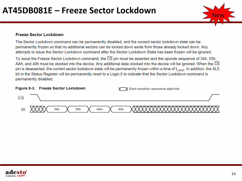
Freeze Sector Lockdown 34h + 55h + AAh + 40h
Program Security Register 9BH + 00H + 00H + 00H 9Bh + 00h + 00h + 00h
Read Security Register 77H 77h
Main Memory Page to Buffer 1 Transfer 53H 53h
Main Memory Page to Buffer 2 Transfer 55H 55h
Main Memory Page to Buffer 1 Compare 60H 60h
Main Memory Page to Buffer 2 Compare 61H 61h
Auto Page Rewrite through Buffer 1 58H 58h
Auto Page Rewrite through Buffer 2 59H 59h
Deep Power-Down B9H B9h
Resume from Deep Power-Down ABH ABh
Ultra-Deep Power-Down 79h
Status Register Read D7H D7h
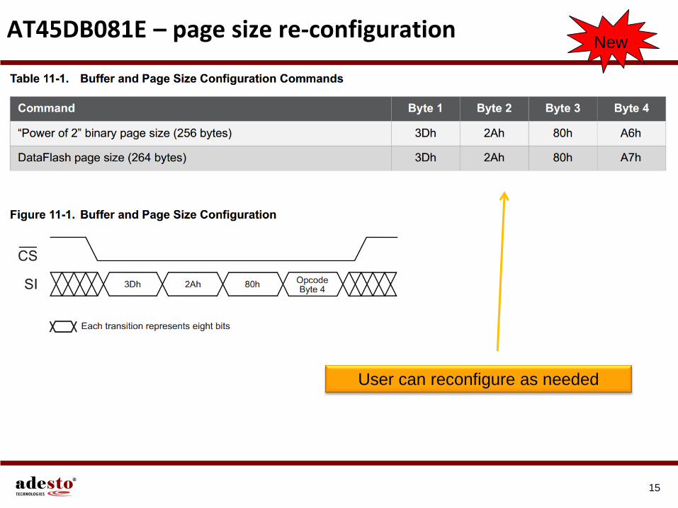
Configure “Power of 2” (Binary) Page Size 3Dh + 2Ah + 80h + A6h 3Dh + 2Ah + 80h + A6h
Configure Standard DataFlash Page Size 3Dh + 2Ah + 80h + A7h
Software Reset F0h + 00h + 00h + 00h
Adesto Technologies CONFIDENTIAL INFORMATION Adesto, the Adesto Logo and CBRAM are Trademarks of Adesto Technologies Corporation
1/31/2014 page #
8
New
New
New
AT45DB081E Command Set Comparison
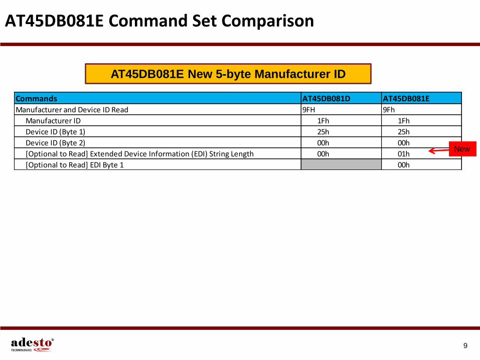
Commands AT45DB081D AT45DB081E
Manufacturer and Device ID Read 9FH 9Fh
Manufacturer ID 1Fh 1Fh
Device ID (Byte 1) 25h 25h
Device ID (Byte 2) 00h 00h
[Optional to Read] Extended Device Information (EDI) String Length 00h 01h
[Optional to Read] EDI Byte 1 00h
9
New
AT45DB081E New 5-byte Manufacturer ID
AT45DB081E Command Set Comparison
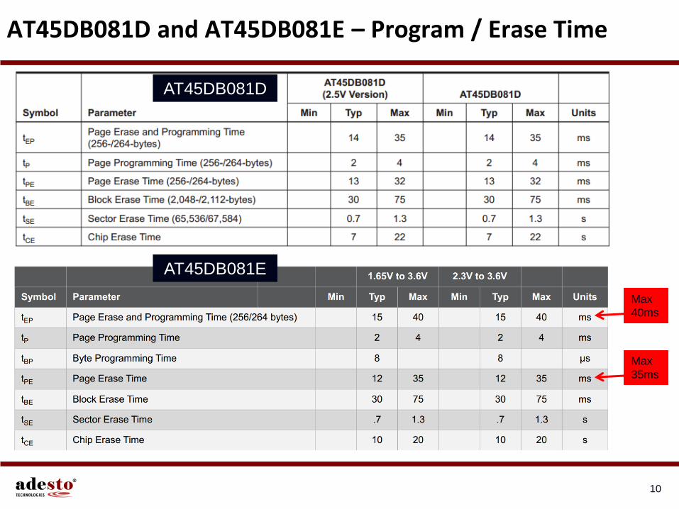
10
AT45DB081D
AT45DB081E
Max
40ms
Max
35ms
AT45DB081D and AT45DB081E – Program / Erase Time
11
No change on the first byte
New
AT45DB081E – New 2-byte Status Register
12
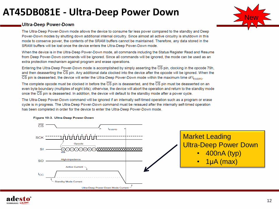
Market Leading
Ultra-Deep Power Down
• 400nA (typ)
• 1μA (max)
New AT45DB081E - Ultra-Deep Power Down
13
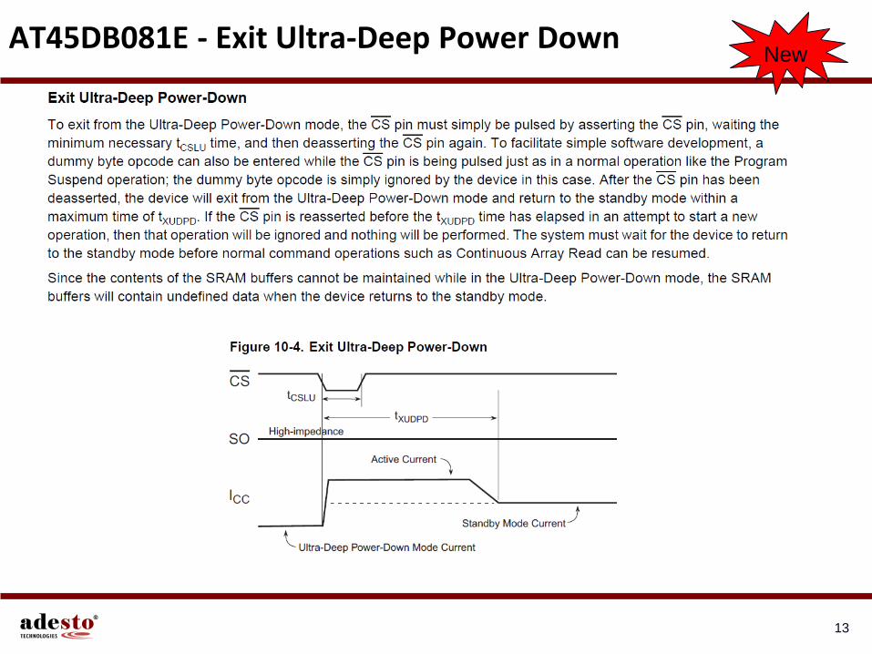
New AT45DB081E - Exit Ultra-Deep Power Down
14
New AT45DB081E – Freeze Sector Lockdown
15
User can reconfigure as needed
New AT45DB081E – page size re-configuration
16
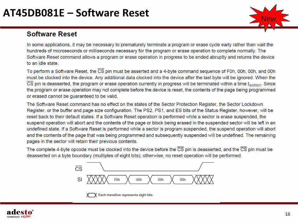
New AT45DB081E – Software Reset
17
New
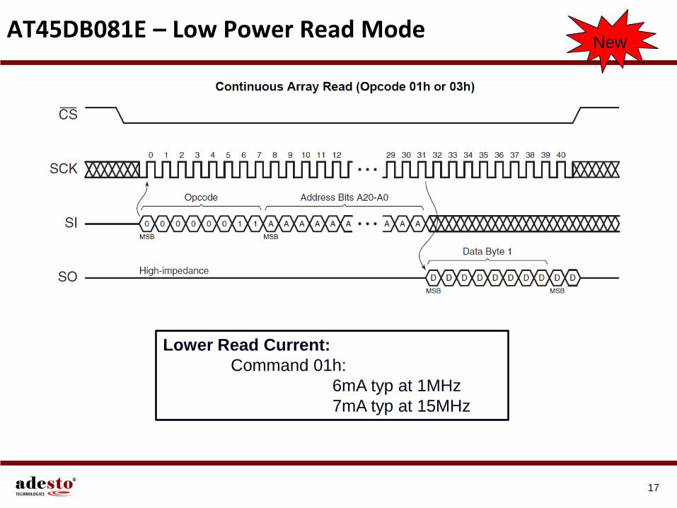
Lower Read Current:
Command 01h:
6mA typ at 1MHz
7mA typ at 15MHz
AT45DB081E – Low Power Read Mode
18
New
Note: Please refer to datasheet for the detail
AT45DB081E – Program / Erase Suspend - Resume
DataFlash® Datasheet:
http://www.adestotech.com/sample-ordering-information
DataFlash® Sample Request:
http://www.adestotech.com/products/serial-flash/dataflash
19
DataFlash DataSheets and Samples