Embed Size (px)
Citation preview
Rev. 32094B-AVR32-05/09
32-bit Microcontroller
Application Note
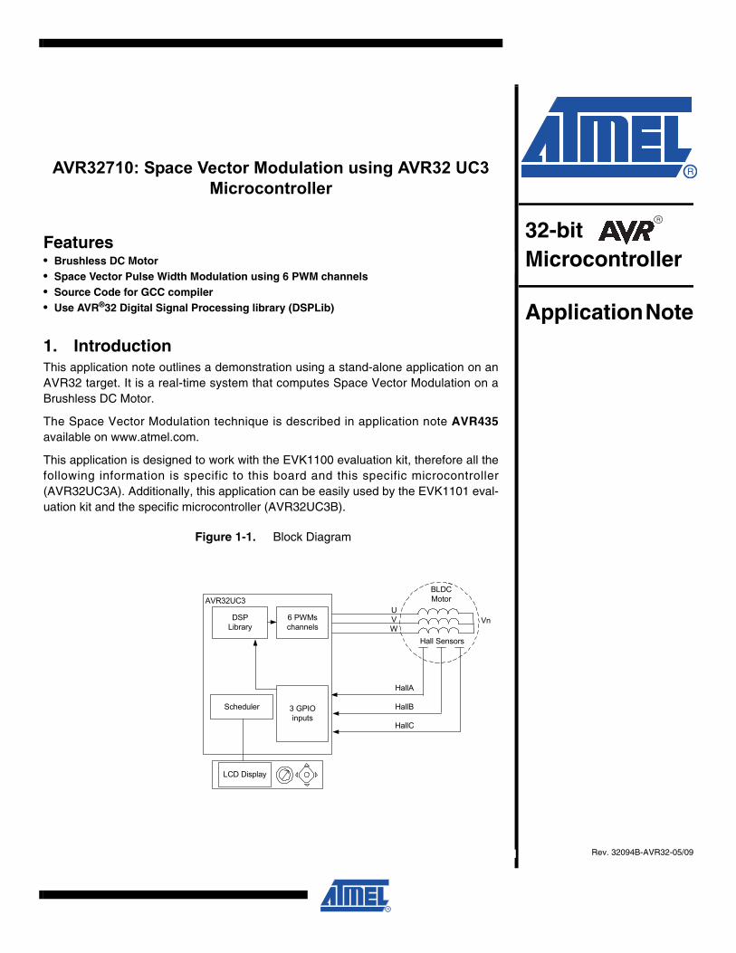
AVR32710: Space Vector Modulation using AVR32 UC3 Microcontroller
Features• Brushless DC Motor • Space Vector Pulse Width Modulation using 6 PWM channels• Source Code for GCC compiler• Use AVR®32 Digital Signal Processing library (DSPLib)
1. IntroductionThis application note outlines a demonstration using a stand-alone application on anAVR32 target. It is a real-time system that computes Space Vector Modulation on aBrushless DC Motor.
The Space Vector Modulation technique is described in application note AVR435available on www.atmel.com.
This application is designed to work with the EVK1100 evaluation kit, therefore all thefollowing information is specific to this board and this specific microcontroller(AVR32UC3A). Additionally, this application can be easily used by the EVK1101 eval-uation kit and the specific microcontroller (AVR32UC3B).
Figure 1-1. Block Diagram
HallA
HallB
HallC
BLDCMotor
Hall Sensors
UVW
Vn6 PWMschannels
3 GPIOinputs
DSPLibrary
Scheduler
LCD Display
AVR32UC3
2. Related PartsThis document applies to the following AT32UC3 parts:
• AT32UC3A0512• AT32UC3A0256• AT32UC3A0128• AT32UC3A1512• AT32UC3A1256• AT32UC3A1128• AT32UC3B0256• AT32UC3B0128• AT32UC3B064• AT32UC3B1256• AT32UC3B1128• AT32UC3B164
3. Related ItemsThe software provided with this application note requires several components:
– AVR32 GNU Toolchain: AVR32 GNU Toolchain is a set of standalone command line programs used to create applications for AVR32 microcontrollers (compiler, assembler, linker, debugger). http://www.atmel.com/dyn/products/tools_card.asp?tool_id=4118
• or– IAR Embedded Workbench® for Atmel AVR32: IAR Embedded Workbench
provides a suite of AVR32 development tools for embedded systems (compiler, assembler, linker, debugger). http://www.iar.com/
• EVK1100: The EVK1100 is an evaluation kit and development system for the AVR32 AT32UC3A microcontroller. http://www.atmel.com/dyn/products/tools_card.asp?tool_id=4114
• EVK1101: The EVK1101 is an evaluation kit and development system for the AVR32 AT32UC3B microcontroller. http://www.atmel.com/dyn/products/tools_card.asp?tool_id=4175
• AVR32 UC3 Software Framework: This framework provides software drivers and libraries to build any application for AVR32 UC3. This is where the DSPLib is located. http://www.atmel.com/dyn/products/tools_card.asp?tool_id=4192
• AT32UC3A0512 Datasheet: http://www.atmel.com/dyn/products/product_card.asp?part_id=4117
• AT32UC3B0256 Datasheet: http://www.atmel.com/dyn/products/product_card.asp?part_id=4174
• Space Vector PWM Software Package: avr32710.zip
232094B–AVR32–05/09
AVR32710

AVR32710
4. Abbreviations• BLDC: Brushless Direct Current• SVPWM : Space Vector Pulse Width Modulation• CW : Clockwise direction / CCW : Counter Clockwise direction• FCPU : CPU frequency• FPBA : Peripheral Bus A frequency
332094B–AVR32–05/09
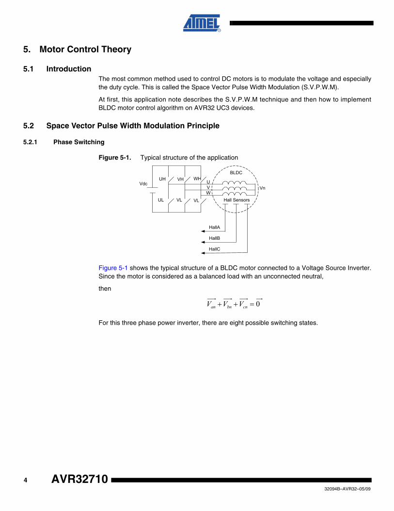
5. Motor Control Theory
5.1 IntroductionThe most common method used to control DC motors is to modulate the voltage and especiallythe duty cycle. This is called the Space Vector Pulse Width Modulation (S.V.P.W.M).
At first, this application note describes the S.V.P.W.M technique and then how to implementBLDC motor control algorithm on AVR32 UC3 devices.
5.2 Space Vector Pulse Width Modulation Principle
5.2.1 Phase Switching
Figure 5-1. Typical structure of the application
Figure 5-1 shows the typical structure of a BLDC motor connected to a Voltage Source Inverter.Since the motor is considered as a balanced load with an unconnected neutral,
then
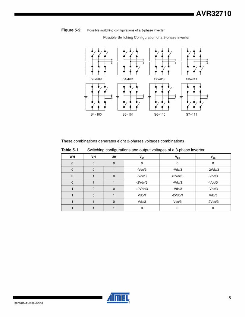
For this three phase power inverter, there are eight possible switching states.
UH
UL
VH
VL VL
WH
HallA
HallB
HallC
BLDC
Hall Sensors
UVW
VnVdc
0=++ cnbnan VVV
432094B–AVR32–05/09
AVR32710
AVR32710
Figure 5-2. Possible switching configurations of a 3-phase inverter
These combinations generates eight 3-phases voltages combinations
Table 5-1. Switching configurations and output voltages of a 3-phase inverter
WH VH UH Van Vbn Vcn
0 0 0 0 0 0
0 0 1 -Vdc/3 -Vdc/3 +2Vdc/3
0 1 0 -Vdc/3 +2Vdc/3 -Vdc/3
0 1 1 -2Vdc/3 -Vdc/3 -Vdc/3
1 0 0 +2Vdc/3 -Vdc/3 -Vdc/3
1 0 1 Vdc/3 -2Vdc/3 Vdc/3
1 1 0 Vdc/3 Vdc/3 -2Vdc/3
1 1 1 0 0 0
Possible Switching Configuration of a 3-phase inverter
532094B–AVR32–05/09
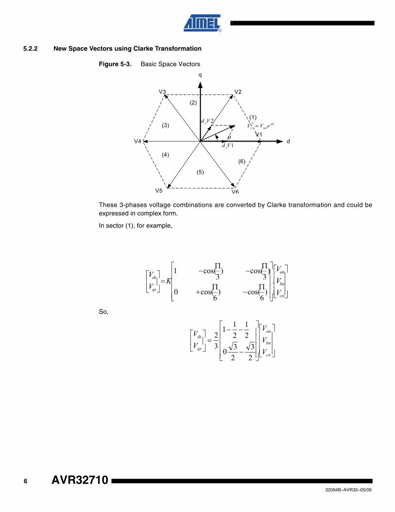
5.2.2 New Space Vectors using Clarke Transformation
Figure 5-3. Basic Space Vectors
These 3-phases voltage combinations are converted by Clarke transformation and could beexpressed in complex form.
In sector (1), for example,
So,
(1)
(2)
(3)
(4)
(5)
(6)
d
q
V1
V2V3
V4
V5 V6
θjsms eVV =*
θ1Vd x
2Vd y
⎥⎥⎥
⎦
⎤
⎢⎢⎢
⎣
⎡
⎥⎥⎥⎥
⎦
⎤
⎢⎢⎢⎢
⎣
⎡
Π−
Π+
Π−
Π−
=⎥⎦
⎤⎢⎣
⎡
cn
bn
an
qs
ds
VVV
KVV
.)6
cos()6
cos(0
)3
cos()3
cos(1
⎥⎥⎥
⎦
⎤
⎢⎢⎢
⎣
⎡
⎥⎥⎥⎥
⎦
⎤
⎢⎢⎢⎢
⎣
⎡
−
−−=⎥
⎦
⎤⎢⎣
⎡
cn
bn
an
qs
ds
VVV
VV
23
230
21
211
32
632094B–AVR32–05/09
AVR32710
AVR32710
It implies as well that switching configuration tables could be expressed in (d-q) format
Each space vector corresponding to WH,VH and UH could be expressed as a combination ofVds and Vqs (vector list in Figure 5-2). This mean for example (WH,VH,UH)=(1,0,0)=V5
5.2.3 Stepping increment and sampling frequencyIn this case, it is possible to define any stator voltage as:
With
As shown in Figure 5-3, the angle decomposes every step of Space Vector computation algo-rithm. As the expression of stator voltage is identical in all the 6 sectors, it is possible to onlycompute equation (1) and (2).
But, every step in computation is given for a angular frequency (in cycles/sec) :
The Ftick is defined as the sampling frequency or the basic frequency of the application. n is theangle stepping increment from the range
For example, with a frequence of tick equal to 20KHz and a resolution up to 8 bits,it is possibleto define a step range from [0;78] thus an angle precision of 0.77 degree.
As the UC3 family has DSP instructions support, the sinus and cosinus computation will be donein software for SVPWM and not with a lookup table. Thus, it is possible to define a specific reso-lution for an application.
Table 5-2. Switching configurations and output voltages of a 3-phase in (d-q) format
WH VH UH Vds Vqs Vector Sector
0 0 1 2Vdc/3 0 V1 (1)
1 1 0 +Vdc/3 +Vdc/3 V2 (2)
0 1 0 -Vdc/3 +Vdc/3 V3 (3)
1 1 0 -2Vdc/3 0 V4 (4)
1 0 0 -Vdc/3 -Vdc/3 V5 (5)
1 0 1 Vdc/3 -Vdc/3 V6 (6)
yyxs UddxUeVV +== θmax
)2()sin(
)1()3
sin(
θ
θ
=
−Π
=
dy
dx
nFticknresolution
××Π
=23
)(θ
⎥⎥⎦
⎤
⎢⎢⎣
⎡resolution
Ftick2;0
732094B–AVR32–05/09
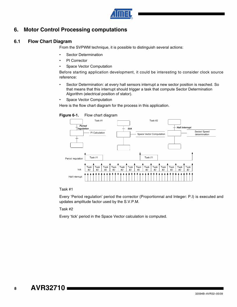
6. Motor Control Processing computations
6.1 Flow Chart DiagramFrom the SVPWM technique, it is possible to distinguish several actions:
• Sector Determination• PI Corrector• Space Vector ComputationBefore starting application development, it could be interesting to consider clock sourcereference:
• Sector Determination: at every hall sensors interrupt a new sector position is reached. So that means that this interrupt should trigger a task that compute Sector Determination Algorithm (electrical position of stator).
• Space Vector ComputationHere is the flow chart diagram for the process in this application.
Figure 6-1. Flow chart diagram
Task #1
Every ‘Period regulation’ period the corrector (Proportionnal and Integer: P.I) is executed andupdates amplitude factor used by the S.V.P.M.
Task #2
Every ‘tick’ period in the Space Vector calculation is computed.
832094B–AVR32–05/09
AVR32710
AVR32710
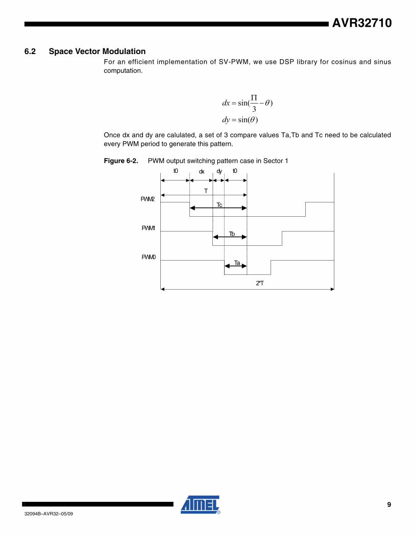
6.2 Space Vector ModulationFor an efficient implementation of SV-PWM, we use DSP library for cosinus and sinuscomputation.
Once dx and dy are calulated, a set of 3 compare values Ta,Tb and Tc need to be calculatedevery PWM period to generate this pattern.
Figure 6-2. PWM output switching pattern case in Sector 1
)sin(
)3
sin(
θ
θ
=
−Π
=
dy
dx
2*T
T
dx dy t0t0
PWM2
PWM1
PWM0
Tc
Tb
Ta
932094B–AVR32–05/09
We can say that for this sector 0:
The Table 6-1 shows all duty cycle values for each sector number. For a sector number the dutycycle for the six half bridge is expressed by:
UH = PWM0 and UL = T-(PWM0)
VH = PWM1 and VL = T-(PWM1)
WH = PWM2 and WL = T-(PWM2)The two rotating directions are described. In case of CCW direction, that means the rotor followsthe sequence Sector number = {6,5,4,3,2,1} and in case of CW direction, the sequence{1,2,3,4,5,6}.
Table 6-1. PWM duty cycle results with SVPWM computation
Sector Number q direction = CCW direction = CW
1
PWM0 = (T - dx -dy)/2
PWM1 = (T + dx -dy)/2
PWM2 = (T + dx + dy)/2
PWM0 = (T + dx + dy)
PWM1 =( T - dx - dy)
PWM2 = (T - dx + dy)
2
PWM0 = (T - dx + dy)/2
PWM1 =( T - dx - dy)/2PWM2 = (T + dx + dy)/2
PWM0 = (T + dx + dy)/2
PWM1 = (T + dx - dy)/2
PWM2 =( T - dx - dy)/2
3
PWM0 = (T + dx + dy)/2
PWM1 = (T - dx - dy)/2
PWM2 = (T + dx - dy)/2
PWM0 = (T - dx + dy)/2PWM1 = (T + dx + dy)/2
PWM2 = (T - dx - dy)/2
4
PWM0 = (T + dx + dy)/2PWM1 = (T -dx + dy)/2
PWM2 = (T - dx + dy)/2
PWM0 = (T - dx -dy)/2
PWM1 = (T + dx + dy)/2PWM2 = (T + dx - dy)/2
5
PWM0 = (T + dx - dy)/2
PWM1 = (T + dx + dy)/2PWM2 = (T - dx - dy)/2
PWM0 = (T - dx - dy)/2
PWM1 = (T - dx + dy)/2
PWM2 = (T + dx + dy)/2
6
PWM0 = (T - dx - dy)/2
PWM1 = (T + dx + dy)/2
PWM2 = (T - dx + dy)/2
PWM0 =( T + dx -dy)/2PWM1 = (T - dx -dy)/2
PWM2 = (T + dx + dy)/2
( )
ac
axb
yxa
TTT
TdT
ddTT
−=
+=
−−=
2
0 π3---[ , ]
π3--- 2π
3------[ , ]
2π3
------ π[ , ]
π 4π3
------[ , ]
4π3
------ 5π3
------[ , ]
5π3
------ 2π[ , ]
1032094B–AVR32–05/09
AVR32710
AVR32710
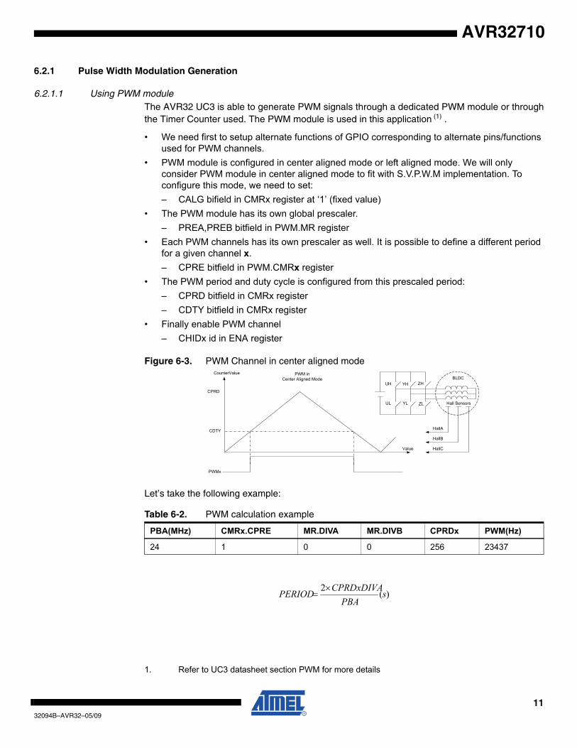
6.2.1 Pulse Width Modulation Generation
6.2.1.1 Using PWM moduleThe AVR32 UC3 is able to generate PWM signals through a dedicated PWM module or throughthe Timer Counter used. The PWM module is used in this application (1) .
• We need first to setup alternate functions of GPIO corresponding to alternate pins/functions used for PWM channels.
• PWM module is configured in center aligned mode or left aligned mode. We will only consider PWM module in center aligned mode to fit with S.V.P.W.M implementation. To configure this mode, we need to set: – CALG bifield in CMRx register at ‘1’ (fixed value)
• The PWM module has its own global prescaler.– PREA,PREB bitfield in PWM.MR register
• Each PWM channels has its own prescaler as well. It is possible to define a different period for a given channel x.– CPRE bitfield in PWM.CMRx register
• The PWM period and duty cycle is configured from this prescaled period:– CPRD bitfield in CMRx register– CDTY bitfield in CMRx register
• Finally enable PWM channel– CHIDx id in ENA register
Figure 6-3. PWM Channel in center aligned mode
Let’s take the following example:
1. Refer to UC3 datasheet section PWM for more details
Table 6-2. PWM calculation example
PBA(MHz) CMRx.CPRE MR.DIVA MR.DIVB CPRDx PWM(Hz)
24 1 0 0 256 23437
CounterValue
Value
CDTY
PWMx
PWM inCenter Aligned Mode
UH
UL
YH
YL ZL
ZH
HallA
HallB
HallC
BLDC
Hall Sensors
CPRD
)(2
sPBA
CPRDxDIVAPERIOD
×=
1132094B–AVR32–05/09
6.3 Tick Reference GenerationThe tick reference is generated with a timer counter usage.
The AVR32 UC3 family is able to generate timer event signals through a dedicated Timer Coun-ter module or through CPU cycle counter mode. Only the Timer Counter is used in thisapplication (1) .
Timer Counter module could be used in Capture Mode or Waveforme Mode. We will only con-sider Timer Counter module in Waveforme mode.
In this mode, the counter will count up until a compare value (RC compare register), reset andrestart from 0x0000. It is possible to generate an interrupt upon RC compare match. This inter-rupt occurs every tick period.
Figure 6-4. Tick generation
• The Timer Counter module has its clock selection source that the user can select:– TCCLKS bitfield in TC.CMR register
• RC compare register will define the periodicity of interrupt:– RC bitfield in TC.RC register
• To enable Timer Counter channel, set:– CLKEN in TC.CCR registe)
Let’s take the following example:
The Tick period value is equal to
1. Refer to UC3 datasheet section Timer Counter for more details
Table 6-3. Timer Counter calculation example
PBA(MHz) CMR.CCLKS CMR.WAVE CMR.WAVESEL RC Tick(Hz)
24 1/(FPBA/8) 1 2 4000 1000
0xFFFF
rc
ra,rb tick0
RCFPBA
tick ×=8/
1
1232094B–AVR32–05/09
AVR32710
AVR32710
6.4 Hall Estimator Each Hall sensor is connected to GPIO. All GPIOs are able to generate interrupts.
By default, interrupts are configured to be used with pin level changes.
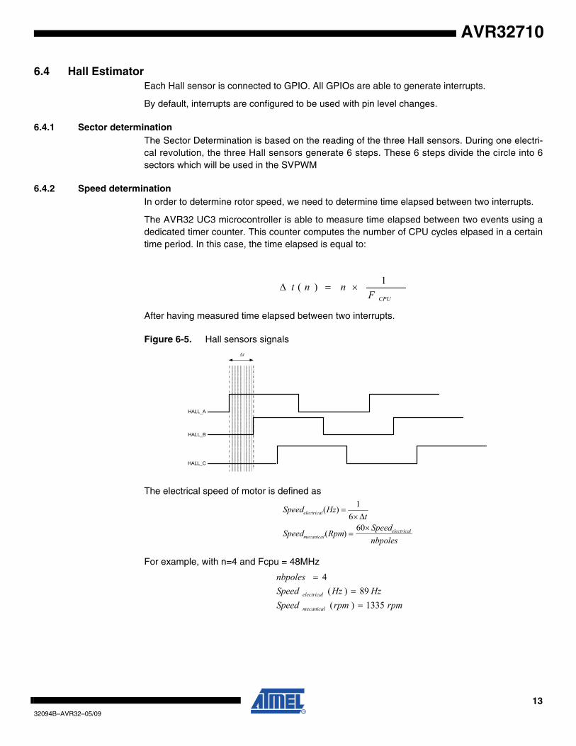
6.4.1 Sector determinationThe Sector Determination is based on the reading of the three Hall sensors. During one electri-cal revolution, the three Hall sensors generate 6 steps. These 6 steps divide the circle into 6sectors which will be used in the SVPWM
6.4.2 Speed determinationIn order to determine rotor speed, we need to determine time elapsed between two interrupts.
The AVR32 UC3 microcontroller is able to measure time elapsed between two events using adedicated timer counter. This counter computes the number of CPU cycles elpased in a certaintime period. In this case, the time elapsed is equal to:
After having measured time elapsed between two interrupts.
Figure 6-5. Hall sensors signals
The electrical speed of motor is defined as
For example, with n=4 and Fcpu = 48MHz
CPUFnnt 1)( ×=Δ
HALL_A
HALL_B
HALL_C
tΔ
nbpolesSpeed
RpmSpeed
tHzSpeed
electricalmecanical
electrical
×=
Δ×=
60)(
61)(
rpmrpmSpeedHzHzSpeed
nbpoles
mecanical
electrical
1335)(89)(
4
==
=
1332094B–AVR32–05/09
7. Software Implementation
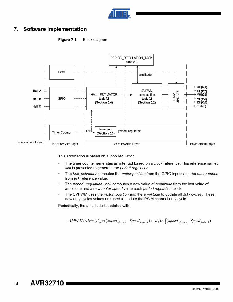
Figure 7-1. Block diagram
This application is based on a loop regulation.
• The timer counter generates an interrupt based on a clock reference. This reference named tick is prescaled to generate the period regulation .
• The hall_estimator computes the motor position from the GPIO inputs and the motor speed from tick reference value.
• The period_regulation_task computes a new value of amplitude from the last value of amplitude and a new motor speed value each period regulation clock.
• The SVPWM uses the motor_position and the amplitude to update all duty cycles. These new duty cycles values are used to update the PWM channel duty cycle.
Periodically, the amplitude is updated with:
Prescalor(Section 5.3)Timer Counter
HALL_ESTIMATORtask #2
(Section 5.4)
PERIOD_REGULATION_TASKtask #1
SVPWMcomputation
task #2(Section 5.2)
Hall A
Hall B
Hall C
UH(Q1)UL(Q2)YH(Q3)YL(Q4)ZH(Q5)ZL(Q6)
PWM
U
PD
ATE
PWM
HARDWARE Layer SOFTWARE Layer Environment Layer
GPIO
Environment Layer
tick
amplitude
period_regulation
∫ −×+−×= )()()()( feedbackreferenceIfeedbackreferencep SpeedSpeedKSpeedSpeedKAMPLITUDE
1432094B–AVR32–05/09
AVR32710
AVR32710
7.1 Source Code Package DescriptionThe software is available in the attached project on the Atmel web Site. The AVR32710.zip con-tains the project for the UC3A0512 Rev. E (engineering samples). The EVK110x-MOTOR-CONTROL-X.Y.Z.ES supports the UC3A0512 Rev. E only.
HTML documentation is included in the package. Use the readme.html file in the doc directory tostart viewing the documentation.
• DRIVERS\This directory contains all libraries used in the project: especially DRIVERS and DSP library
support.
• SERVICES\MOTOR_CONTROL\– HALL_ESTIMATOR\
This directory contains the service to determine rotor position (angle and sector).– MOTOR_DRIVER\BLDC_MOTOR\
This directory contains the service for low level drive of PWM channels.– SVPWM\
This directory contains the Space Vector computation algorithm.
• APPLICATIONS\EVK110x-MOTOR-CONTROL\BLDC-SVPWM\EXAMPLE\– bldc_svpwm_example.c
This file contains the main() with all CPU initialization and task launch.– mc_control.c
This file defines the main control loop sequence.– mc_driver.c
This files defines the low level loop sequence access.– sensor_task.c
This files defines dedicated task function for display and motor control.
7.2 CPU Load & Memory Usage
The following benchmarks have been done on AVR32-GCC 4.2.2-atmel.1.0.4 with this
configuration• FCPU = 42MHz• FPBA = 21MHz
Table 7-1. Microcontroller utilization rate
Function ParametersActivation time
Activation period
COMPARE_INT_HANDLER HALL_ESTIMATOR 5us 64usSVPWM_COMPUTATION 20us 64us
1532094B–AVR32–05/09
8. Hardware Implementation
8.1 EVK1100 Connection
The Table 8-1 lists the connections between evaluation kit and motor connection.
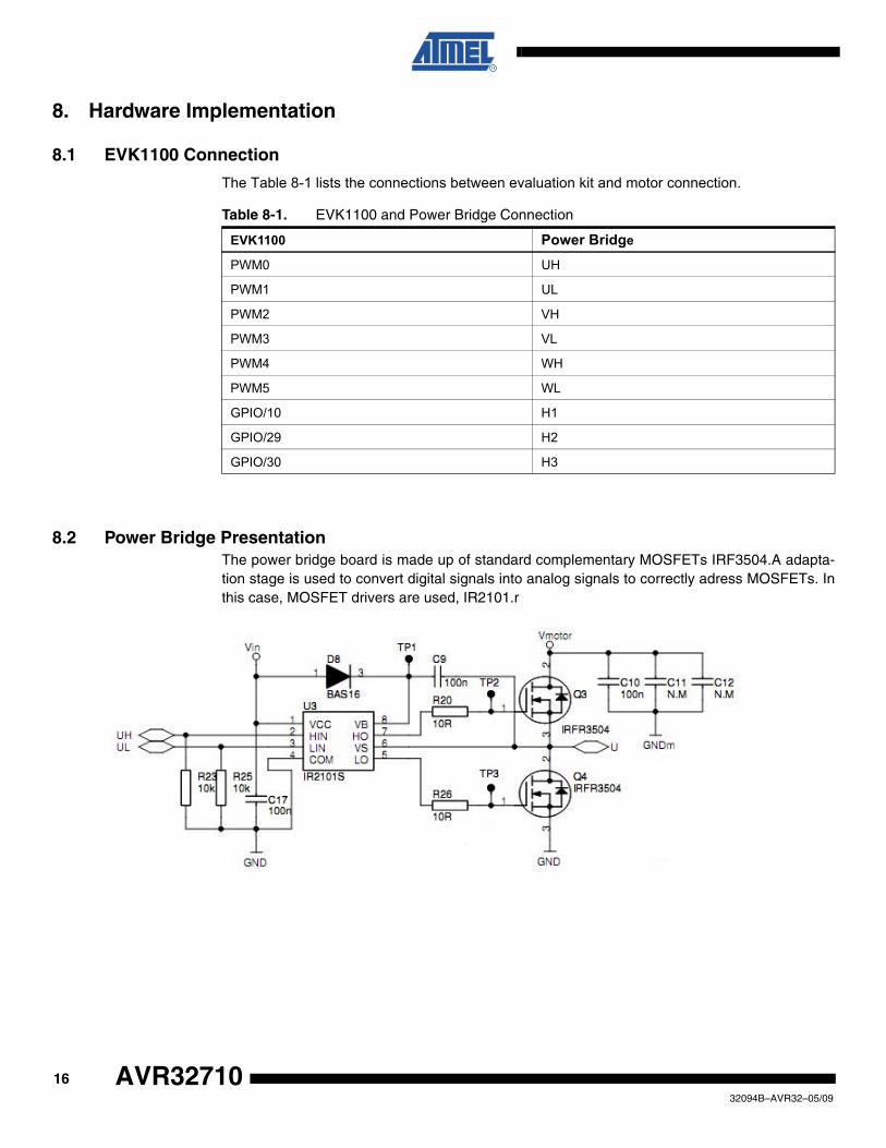
8.2 Power Bridge PresentationThe power bridge board is made up of standard complementary MOSFETs IRF3504.A adapta-tion stage is used to convert digital signals into analog signals to correctly adress MOSFETs. Inthis case, MOSFET drivers are used, IR2101.r
Table 8-1. EVK1100 and Power Bridge Connection
EVK1100 Power Bridge
PWM0 UH
PWM1 UL
PWM2 VH
PWM3 VL
PWM4 WH
PWM5 WL
GPIO/10 H1
GPIO/29 H2
GPIO/30 H3
1632094B–AVR32–05/09
AVR32710
AVR32710
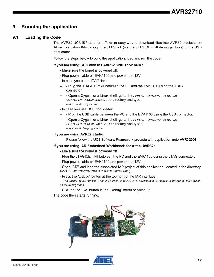
9. Running the application
9.1 Loading the CodeThe AVR32 UC3 ISP solution offers an easy way to download files into AVR32 products onAtmel Evaluation Kits through the JTAG link (via the JTAGICE mkII debugger tools) or the USBbootloader.
Follow the steps below to build the application, load and run the code:
If you are using GCC with the AVR32 GNU Toolchain :- Make sure the board is powered off.- Plug power cable on EVK1100 and power it at 12V.- In case you use a JTAG link:– - Plug the JTAGICE mkII between the PC and the EVK1100 using the JTAG
connector.– - Open a Cygwin or a Linux shell, go to the APPLICATIONS/EVK110x-MOTOR-
CONTORL/AT32UC3A0512ES/GCC directory and type :make rebuild program run
- In case you use USB bootloader:– - Plug the USB cable between the PC and the EVK1100 using the USB connector.– - Open a Cygwin or a Linux shell, go to the APPLICATIONS/EVK110x-MOTOR-
CONTORL/AT32UC3A0512ES/GCC directory and type :make rebuild isp program run
If you are using AVR32 Studio:– Please follow the UC3 Software Framework procedure in application note AVR32008
If you are using IAR Embedded Workbench for Atmel AVR32:- Make sure the board is powered off.- Plug the JTAGICE mkII between the PC and the EVK1100 using the JTAG connector.- Plug power cable on EVK1100 and power it at 12V.- Open IAR® and load the associated IAR project of this application (located in the directory EVK110x-MOTOR-CONTORL/AT32UC3A0512ES/IAR ).- Press the “Debug” button at the top right of the IAR interface.
The project should compile. Then the generated binary file is downloaded to the microcontroller to finally switch on the debug mode.
- Click on the “Go” button in the “Debug” menu or press F5.The code then starts running.
1732094B–AVR32–05/09
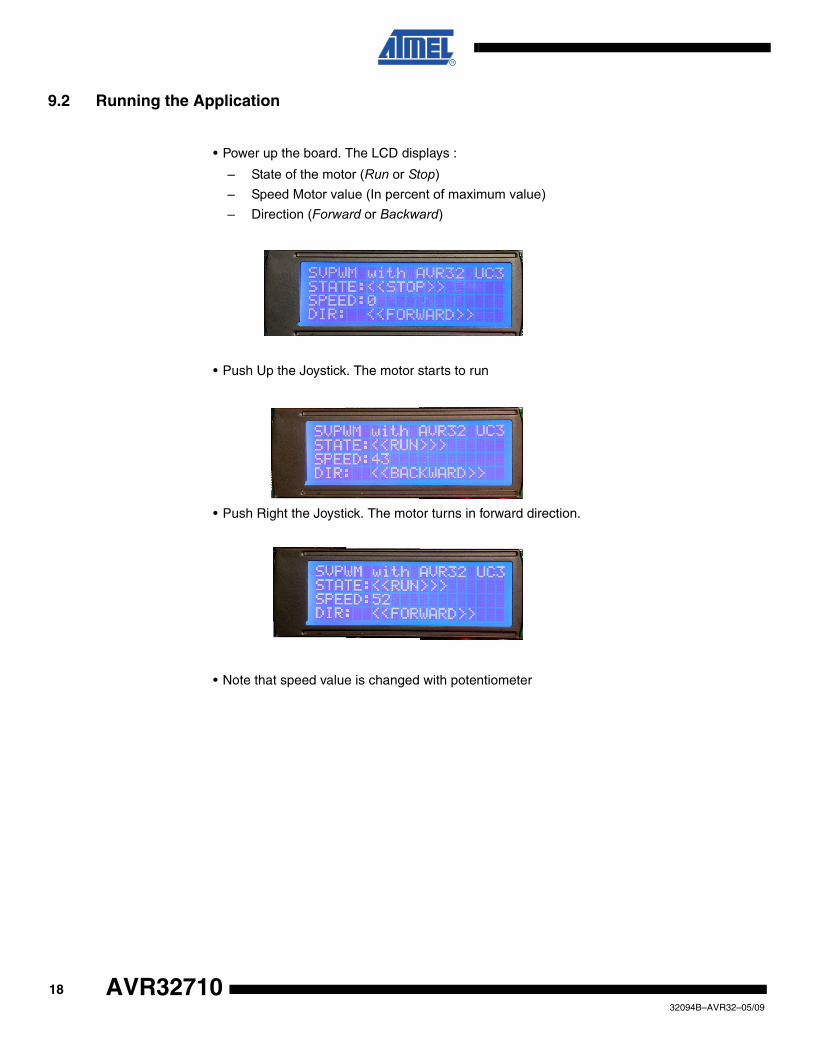
9.2 Running the Application
• Power up the board. The LCD displays :
– State of the motor (Run or Stop)– Speed Motor value (In percent of maximum value)– Direction (Forward or Backward)
• Push Up the Joystick. The motor starts to run
• Push Right the Joystick. The motor turns in forward direction.
• Note that speed value is changed with potentiometer
1832094B–AVR32–05/09
AVR32710
Headquarters International
Atmel Corporation2325 Orchard ParkwaySan Jose, CA 95131USATel: 1(408) 441-0311Fax: 1(408) 487-2600
Atmel AsiaUnit 1-5 & 16, 19/FBEA Tower, Millennium City 5418 Kwun Tong RoadKwun Tong, KowloonHong KongTel: (852) 2245-6100Fax: (852) 2722-1369
Atmel EuropeLe Krebs8, Rue Jean-Pierre TimbaudBP 30978054 Saint-Quentin-en-Yvelines CedexFranceTel: (33) 1-30-60-70-00 Fax: (33) 1-30-60-71-11
Atmel Japan9F, Tonetsu Shinkawa Bldg.1-24-8 ShinkawaChuo-ku, Tokyo 104-0033JapanTel: (81) 3-3523-3551Fax: (81) 3-3523-7581
Product Contact
Web Sitewww.atmel.com
Technical [email protected]
Sales Contactwww.atmel.com/contacts
Literature Requestswww.atmel.com/literature
Disclaimer: The information in this document is provided in connection with Atmel products. No license, express or implied, by estoppel or otherwise, to anyintellectual property right is granted by this document or in connection with the sale of Atmel products. EXCEPT AS SET FORTH IN ATMEL’S TERMS AND CONDI-TIONS OF SALE LOCATED ON ATMEL’S WEB SITE, ATMEL ASSUMES NO LIABILITY WHATSOEVER AND DISCLAIMS ANY EXPRESS, IMPLIED OR STATUTORYWARRANTY RELATING TO ITS PRODUCTS INCLUDING, BUT NOT LIMITED TO, THE IMPLIED WARRANTY OF MERCHANTABILITY, FITNESS FOR A PARTICULARPURPOSE, OR NON-INFRINGEMENT. IN NO EVENT SHALL ATMEL BE LIABLE FOR ANY DIRECT, INDIRECT, CONSEQUENTIAL, PUNITIVE, SPECIAL OR INCIDEN-TAL DAMAGES (INCLUDING, WITHOUT LIMITATION, DAMAGES FOR LOSS OF PROFITS, BUSINESS INTERRUPTION, OR LOSS OF INFORMATION) ARISING OUT OFTHE USE OR INABILITY TO USE THIS DOCUMENT, EVEN IF ATMEL HAS BEEN ADVISED OF THE POSSIBILITY OF SUCH DAMAGES. Atmel makes norepresentations or warranties with respect to the accuracy or completeness of the contents of this document and reserves the right to make changes to specificationsand product descriptions at any time without notice. Atmel does not make any commitment to update the information contained herein. Unless specifically providedotherwise, Atmel products are not suitable for, and shall not be used in, automotive applications. Atmel’s products are not intended, authorized, or warranted for useas components in applications intended to support or sustain life.
© 2009 Atmel Corporation. All rights reserved. Atmel®, Atmel logo and combinations thereof, AVR®32 and others are registered trademarks ortrademarks of Atmel Corporation or its subsidiaries. Other terms and product names may be trademarks of others.
32094B–AVR32–05/09