Embed Size (px)
Citation preview
RELIABILITY ISSUES IN GERMANIUM AND SILICON
CARBIDE MOS DEVICES
By
Rajan Arora
Thesis
Submitted to the Faculty of the
Graduate school of Vanderbilt University
in partial fulfillment of the requirements
For the degree of
MASTER OF SCIENCE
in
Electrical Engineering
August, 2009
Nashville, Tennessee
Approved by:
Professor Ronald D. Schrimpf
Professor Daniel M. Fleetwood
ii
© Copyright by Rajan Arora 2009
All Rights Reserved
iii
To My Mother & Sisters
who always stood by me in good and bad times
iv
ACKNOWLEDGEMENTS
I would first of all like to thank Prof. Ron Schrimpf for showing faith in my abilities
throughout my stay at Vanderbilt. His research thought process, teaching and presenta-
tion skills always influenced me.
I would also like to thank Prof. Dan Fleetwood for his useful comments and support
for my research. His immense experimental and physical knowledge always helped me in
my work.
I would like to thank Dean Ken Galloway for his support and encouragement during
the course of this work and the professors who helped me create strong basics in mathe-
matics, physics, and engineering.
I thank collaborators at NCSU, IMEC and Griffith University for the success of this
work. I thank AFOSR and Vanderbilt School of Engineering for providing the funds for
this work.
I would like to thank all the friends I had starting from primary school to graduate
school. Chetan, Aditya, Deepti, Shweta, Tripti, Tina, Aparna, Puja, Saumitra, Sameer,
Sriram, Farah, Kulkarni, Bo, John, Nikkon, Srikanth, Vishwa, Tania, David, Nadia, Dan-
iel, Jon, Ashley, Jonny, Hyunwoo, Sandeepan, Megan, Andrew, Wole, Rishab, Ankur,
Nitin, Abhishek, Mayur, Rahul, Anuj, Gaurav, Sumit, Rohit, Rachita, Lovina, Malvika
for their friendship.
Last but not least I thank my sisters (Prerna, Vaishali, Puja, Manjari), my mother
(Mrs. Raj Arora), my brother-in-laws (Sanjay, Rajiv, Vishal), and my nieces and neph-
ews (Aparna, Alisha, Daksh, Shreyas) for everything they have done for me.
v
TABLE OF CONTENTS
Page
ACKNOWLEDGEMENTS........................................................................................ iv
LIST OF FIGURES ……………………………………………………..……....vii-xi
I. ALTERNATIVE SUBSTRATE MOS DEVICES............................................ 1 I) INTRODUCTION ................................................................................................... 1 II) HIGH-κ DIELECTRICS.......................................................................................... 5 III) ALTERNATIVE SUBSTRATE MOSFETS .............................................................. 7
A) Ge p-MOSFETs............................................................................................ 7 B) III-V n-MOSFETs......................................................................................... 8
IV) SIC POWER MOS DEVICES ................................................................................. 9 A) Polytypes of SiC ......................................................................................... 10 B) Properties of nitrided oxides on SiC .......................................................... 11 C) SiC/SiO2 interface trap spectrum ............................................................... 13
V) CONCLUSIONS .................................................................................................. 15
II. BASICS OF TOTAL DOSE RADIATION AND BIAS TEMPERATURE INSTABILITY…………................................................................................... 16
I) RADIATION DAMAGE......................................................................................... 16 A) Experimental setup for x-ray radiation...................................................... 18 B) Optimum lab source for radiation testing.................................................. 18 C) Total dose effects on MOS devices ............................................................. 19 D) Total dose radiation in high-κ dielectric MOS devices ............................. 25
II) NEGATIVE BIAS TEMPERATURE INSTABILITY (NBTI)...................................... 25 A) What is NBTI? ............................................................................................ 25 B) NBTI models............................................................................................... 26 C) Interface traps and oxide charges .............................................................. 27
III. RADIATION EFFECTS ON GERMANIUM P-MOSFETS-PART I: BASIC MECHANISMS.................................................................................... 33
I) EXPERIMENTAL DETAILS .................................................................................. 34 II) EFFECT OF RADIATION ON DRAIN-SUBSTRATE JUNCTION LEAKAGE.................. 37 III) MECHANISMS THAT CAUSE THE INCREASE IN JUNCTION LEAKAGE WITH
RADIATION....................................................................................................... 42 IV) CONCLUSION.................................................................................................... 45
IV. RADIATION EFFECTS ON GERMANIUM P-MOSFETS-PART II: UNDERSTANDING EFFECT OF VARIATION IN HALO DOPING AND SI MONOLAYER THICKNESS ON TOTAL-DOSE RESPONSE OF GE P-MOSFETS......................................................................................... 47
I) DEVICE AND EXPERIMENTAL DETAILS............................................................... 48
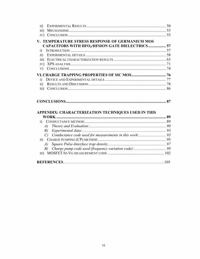
vi
II) EXPERIMENTAL RESULTS................................................................................. 50 III) MECHANISMS................................................................................................... 53 IV) CONCLUSION.................................................................................................... 55
V. TEMPERATURE STRESS RESPONSE OF GERMANIUM MOS CAPACITORS WITH HFO2/HFSION GATE DIELECTRICS.................. 57
I) INTRODUCTION ................................................................................................. 57 II) EXPERIMENTAL DETAILS.................................................................................. 58 III) ELECTRICAL CHARACTERIZATION RESULTS ..................................................... 63 IV) XPS ANALYSIS................................................................................................. 71 V) CONCLUSIONS .................................................................................................. 74
VI. CHARGE TRAPPING PROPERTIES OF SIC MOS................................... 76 I) DEVICE AND EXPERIMENTAL DETAILS .............................................................. 77 II) RESULTS AND DISCUSSION............................................................................... 78 III) CONCLUSION.................................................................................................... 86
CONCLUSIONS...................................................................................................... 87
APPENDIX: CHARACTERIZATION TECHNIQUES USED IN THIS WORK................................................................................................................ 89
I) CONDUCTANCE METHOD................................................................................... 89 A) Theory and Evaluation:.............................................................................. 90 B) Experimental data:..................................................................................... 93 C) Conductance code used for measurements in this work:........................... 93
II) CHARGE PUMPING (CP) METHOD ..................................................................... 95 A) Square Pulse-Interface trap density........................................................... 97 B) Charge pump code used (frequency variation code): ................................ 98
III) MOSFET ID-VG MEASUREMENT CODE ......................................................... 102 REFERENCES…………………………………………………………….……..105
vii
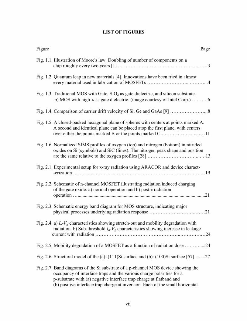
LIST OF FIGURES
Figure Page
Fig. 1.1. Illustration of Moore's law: Doubling of number of components on a chip roughly every two years [1] .…………………………………………….…3 Fig. 1.2. Quantum leap in new materials [4]. Innovations have been tried in almost every material used in fabrication of MOSFETs ……………………...………...4
Fig. 1.3. Traditional MOS with Gate, SiO2 as gate dielectric, and silicon substrate. b) MOS with high-κ as gate dielectric. (image courtesy of Intel Corp.) ……….6 Fig. 1.4. Comparison of carrier drift velocity of Si, Ge and GaAs [9] …………………...8
Fig. 1.5. A closed-packed hexagonal plane of spheres with centers at points marked A. A second and identical plane can be placed atop the first plane, with centers over either the points marked B or the points marked C ………………………11 Fig. 1.6. Normalized SIMS profiles of oxygen (top) and nitrogen (bottom) in nitrided oxides on Si (symbols) and SiC (lines). The nitrogen peak shape and position are the same relative to the oxygen profiles [28] …………………………...….13
Fig. 2.1. Experimental setup for x-ray radiation using ARACOR and device charact- -erization ……………………………………………………………………….19 Fig. 2.2. Schematic of n-channel MOSFET illustrating radiation induced charging of the gate oxide: a) normal operation and b) post-irradiation operation ….........................................................................................................21
Fig. 2.3. Schematic energy band diagram for MOS structure, indicating major physical processes underlying radiation response ………………………..……21
Fig. 2.4. a) Id-Vg characteristics showing stretch-out and mobility degradation with radiation. b) Sub-threshold Id-Vg characteristics showing increase in leakage current with radiation ……………………………………………..………….…24
Fig. 2.5. Mobility degradation of a MOSFET as a function of radiation dose ……….....24 Fig. 2.6. Structural model of the (a): (111)Si surface and (b): (100)Si surface [57] …....27
Fig. 2.7. Band diagrams of the Si substrate of a p-channel MOS device showing the occupancy of interface traps and the various charge polarities for a p-substrate with (a) negative interface trap charge at flatband and (b) positive interface trap charge at inversion. Each of the small horizontal
viii
lines represents an interface trap. It is either occupied by an electron (solid circle) or occupied by a hole (unoccupied by an electron), shown by the lines ……………………………………………………………………………...29
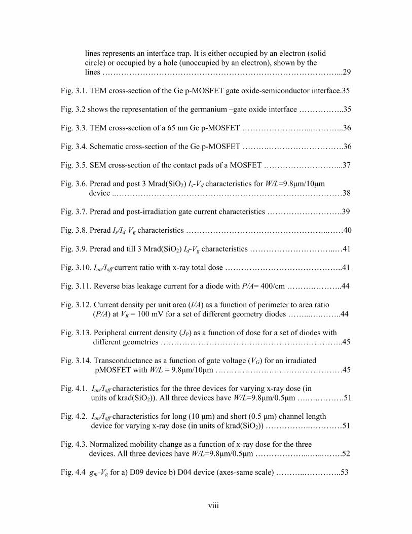
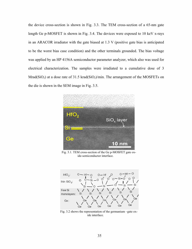
Fig. 3.1. TEM cross-section of the Ge p-MOSFET gate oxide-semiconductor interface.35
Fig. 3.2 shows the representation of the germanium –gate oxide interface ……………..35 Fig. 3.3. TEM cross-section of a 65 nm Ge p-MOSFET ……………………...………...36 Fig. 3.4. Schematic cross-section of the Ge p-MOSFET ……….……………………….36
Fig. 3.5. SEM cross-section of the contact pads of a MOSFET ………………………...37
Fig. 3.6. Prerad and post 3 Mrad(SiO2) Is-Vd characteristics for W/L=9.8µm/10µm device ..…………………………………………………………………………38
Fig. 3.7. Prerad and post-irradiation gate current characteristics ……………………….39
Fig. 3.8. Prerad Is/Id-Vg characteristics ……………………………………………..……40
Fig. 3.9. Prerad and till 3 Mrad(SiO2) Id-Vg characteristics …………………………..…41
Fig. 3.10. Ion/Ioff current ratio with x-ray total dose ……………………………………..41
Fig. 3.11. Reverse bias leakage current for a diode with P/A= 400/cm ……….………..44
Fig. 3.12. Current density per unit area (I/A) as a function of perimeter to area ratio (P/A) at VR = 100 mV for a set of different geometry diodes ……...….……..44
Fig. 3.13. Peripheral current density (JP) as a function of dose for a set of diodes with different geometries …………………………………………………………..45
Fig. 3.14. Transconductance as a function of gate voltage (VG) for an irradiated pMOSFET with W/L = 9.8µm/10µm ………………….…..…………………45
Fig. 4.1. Ion/Ioff characteristics for the three devices for varying x-ray dose (in units of krad(SiO2)). All three devices have W/L=9.8µm/0.5µm ….….……….51
Fig. 4.2. Ion/Ioff characteristics for long (10 µm) and short (0.5 µm) channel length device for varying x-ray dose (in units of krad(SiO2)) ……………..…………51
Fig. 4.3. Normalized mobility change as a function of x-ray dose for the three devices. All three devices have W/L=9.8µm/0.5µm ………………...…...…….52 Fig. 4.4 gm-Vg for a) D09 device b) D04 device (axes-same scale) ………..…………..53
ix
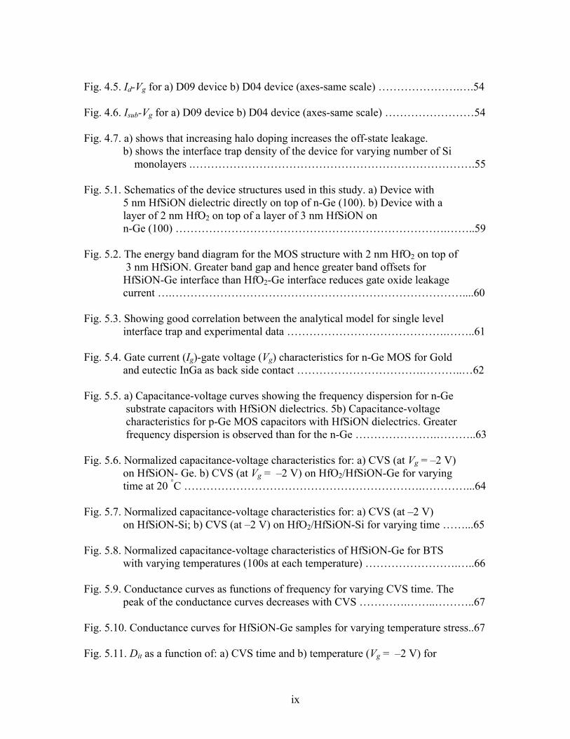
Fig. 4.5. Id-Vg for a) D09 device b) D04 device (axes-same scale) ………………….….54 Fig. 4.6. Isub-Vg for a) D09 device b) D04 device (axes-same scale) ……………………54 Fig. 4.7. a) shows that increasing halo doping increases the off-state leakage. b) shows the interface trap density of the device for varying number of Si monolayers .………………………………………………………………….55 Fig. 5.1. Schematics of the device structures used in this study. a) Device with 5 nm HfSiON dielectric directly on top of n-Ge (100). b) Device with a layer of 2 nm HfO2 on top of a layer of 3 nm HfSiON on n-Ge (100) ……………………………………………………………….……..59 Fig. 5.2. The energy band diagram for the MOS structure with 2 nm HfO2 on top of 3 nm HfSiON. Greater band gap and hence greater band offsets for HfSiON-Ge interface than HfO2-Ge interface reduces gate oxide leakage current ….……………………………………………………………………....60 Fig. 5.3. Showing good correlation between the analytical model for single level interface trap and experimental data …………………………………….……..61 Fig. 5.4. Gate current (Ig)-gate voltage (Vg) characteristics for n-Ge MOS for Gold and eutectic InGa as back side contact …………………………….………..…62 Fig. 5.5. a) Capacitance-voltage curves showing the frequency dispersion for n-Ge substrate capacitors with HfSiON dielectrics. 5b) Capacitance-voltage characteristics for p-Ge MOS capacitors with HfSiON dielectrics. Greater frequency dispersion is observed than for the n-Ge ………………….………..63 Fig. 5.6. Normalized capacitance-voltage characteristics for: a) CVS (at Vg = –2 V) on HfSiON- Ge. b) CVS (at Vg = –2 V) on HfO2/HfSiON-Ge for varying time at 20 °C ……………………………………………………….…………...64 Fig. 5.7. Normalized capacitance-voltage characteristics for: a) CVS (at –2 V) on HfSiON-Si; b) CVS (at –2 V) on HfO2/HfSiON-Si for varying time ……...65 Fig. 5.8. Normalized capacitance-voltage characteristics of HfSiON-Ge for BTS with varying temperatures (100s at each temperature) …………………….…..66 Fig. 5.9. Conductance curves as functions of frequency for varying CVS time. The peak of the conductance curves decreases with CVS ………….……..………..67 Fig. 5.10. Conductance curves for HfSiON-Ge samples for varying temperature stress..67 Fig. 5.11. Dit as a function of: a) CVS time and b) temperature (Vg = –2 V) for
x
HfSiON- Ge MOS capacitors (100 s at each temperature) ………….........…....69 Fig. 5.12. Border trap (Nbt) density for a) different CVS time (HfSiON- Ge) and b) varying BTS temperature (HfSiON- Ge) …………………………….……70 Fig. 5.13. XPS survey of an Al/ HfSiON/Ge capacitor after thinning the electrode with argon sputtering …………………………………………………………72 Fig. 5.14. High-resolution XPS spectra collected from heated and unheated capacitors after the electrode was thinned using argon sputtering …………...74 Fig. 6.1. Schematic of the MOS capacitor used in this study …...…………….………..78 Fig. 6.2. Interface trap density, Dit, as a function of energy for 4H- and 3C-SiC samples ………………………………….………………………………….…..79 Fig. 6.3. Capacitance/conductance-voltage characteristics for 4H-SiC MOS with N2O treatment ……………………….………………………………………....79 Fig. 6.4. Shift in midgap voltage as a function of x-ray dose for 3C-SiC MOS with NO treated oxide ………………………..………………………………...81
Fig. 6.5. Shift in midgap voltage as a function of x-ray dose for 3C-SiC MOS with N2O treated oxide …………………………………………….…………...81
Fig. 6.6. Midgap voltage shift as a function of x-ray dose for 4H-SiC MOS with NO treated oxide ………………………………………..………………..82
Fig. 6.7. Normalized midgap voltage shift comparison for a 4H-/3C-SiC MOS sample ……………………………………………………………..…………...84
Fig. 6.8. Nitrogen concentration as a function of depth for 4H MOS capacitors with NO and N2O nitridation …………………………..………………………85 Fig. 6.9. Nitrogen concentration as a function of depth for 3C MOS capacitors with NO and N2O nitridation …………………………………..……………....85
Fig. A.1. MOS equivalent circuit ...………………………………...………………..…92 Fig. A.2. a). Capacitance-angular frequency (C-ω) characteristics for a Ge MOS capacitor. b) Conductance-angular frequency (G-ω) characteristic for same sample. c) Equivalent parallel conductance divided by angular frequency as a function of frequency …………………………….………..…93 Fig. A.3. Circuit diagram used in charge pump measurement ……………………….….97
xi
Fig. A.4. Schematic illustration of a square-pulse charge pump method applied to a n-MOSFET ……………………………………………………..………....98
1
CHAPTER I
ALTERNATIVE SUBSTRATE MOS DEVICES
i) Introduction
Silicon has been the material of choice for commercial MOS devices for four dec-
ades because it has excellent material and electrical properties. To improve device per-
formance the channel length and gate oxide thickness have been historically scaled down
starting from a channel length of a few micrometers to the present day’s 45 nm technol-
ogy node. For decades now technology scaling has allowed ever improving computing
performance. MOSFET scaling has allowed an increasing number of components on an
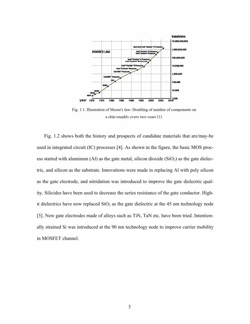
integrated circuit (IC) as seen in Fig. 1.1 for the years since 1970 [1]. The scaling of the
MOSFET has allowed increased functionality per unit chip-area, reduced cost per func-
tionality, increased performance, and reduced device-switching power. Better gate con-
trol was achieved in short channel MOSFETs by decreasing the gate oxide thickness.
Gate oxide thicknesses have been scaled from a few hundred nanometers to less than one
nm during this process. For future device performance improvement it is no longer possi-
ble to scale the gate oxide thickness, as the oxide thickness has reached limits where the
gate tunneling current becomes too high.
The properties of silicon dioxide have been key to the success of the CMOS industry
due to the high electrical quality of the Si/SiO2 interface, its favorable material properties
and reliability. Dielectric materials with a higher-κ (relative dielectric constant) value
maintain channel control for larger thicknesses and improve drive current. The introduc-
2
tion of high-κ gate dielectrics along with metal gate technology, which resolved the gate
leakage issue in 45 nm MOSFETs [2], is deemed one of the largest innovations in CMOS
technology since the introduction of the poly gate, or even the invention of the MOS in-
tegrated circuit itself. Several other technological features have been included in produc-
tion MOSFETs recently to propel CMOS along the roadmap, such as lowering the κ-
value of interconnect dielectrics to reduce interconnect delay, advanced channel strain
techniques to boost performance, and numerous other innovations.
However, high-κ materials may result in degraded carrier mobility in the inversion
layer. Therefore, new materials are being looked at as alternative substrate materials for
MOS devices. Among them, germanium and III-V substrates (such as GaAs, InGaAs,
etc.) are the most important ones. These materials provide higher carrier (electron and
hole) mobilities. However, there are many problems associated with fabrication of MOS-
FETS on these materials such as the absence of a stable native oxide, intrinsic defects
present in the material or finding appropriate dopants. Making MOSFETs on these mate-
rials that can meet the on and off current specs described in the ITRS roadmap is an area
of active research [3].
3
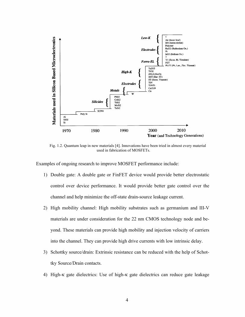
Fig. 1.2 shows both the history and prospects of candidate materials that are/may-be
used in integrated circuit (IC) processes [4]. As shown in the figure, the basic MOS proc-
ess started with aluminum (Al) as the gate metal, silicon dioxide (SiO2) as the gate dielec-
tric, and silicon as the substrate. Innovations were made in replacing Al with poly silicon
as the gate electrode, and nitridation was introduced to improve the gate dielectric qual-
ity. Silicides have been used to decrease the series resistance of the gate conductor. High-
κ dielectrics have now replaced SiO2 as the gate dielectric at the 45 nm technology node
[5]. New gate electrodes made of alloys such as TiN, TaN etc. have been tried. Intention-
ally strained Si was introduced at the 90 nm technology node to improve carrier mobility
in MOSFET channel.
Fig. 1.1. Illustration of Moore's law: Doubling of number of components on
a chip roughly every two years [1].
4
Examples of ongoing research to improve MOSFET performance include:
1) Double gate: A double gate or FinFET device would provide better electrostatic
control over device performance. It would provide better gate control over the
channel and help minimize the off-state drain-source leakage current.
2) High mobility channel: High mobility substrates such as germanium and III-V
materials are under consideration for the 22 nm CMOS technology node and be-
yond. These materials can provide high mobility and injection velocity of carriers
into the channel. They can provide high drive currents with low intrinsic delay.
3) Schottky source/drain: Extrinsic resistance can be reduced with the help of Schot-
tky Source/Drain contacts.
4) High-κ gate dielectrics: Use of high-κ gate dielectrics can reduce gate leakage
Fig. 1.2. Quantum leap in new materials [4]. Innovations have been tried in almost every material
used in fabrication of MOSFETs.
5
current and hence power consumption.
5) Metal gate: Gate depletion problems that occur with poly-Si gate electrodes can
be solved with use of metal gates.
ii) High-κ dielectrics
High-κ dielectrics were introduced into IC’s because SiO2 gate dielectrics were get-
ting thinner and thinner and reached the level where they were only a few atomic layers
thick. SiO2 is an excellent insulator, but at this thickness, the tunneling current through
the gate electrode is significant. Therefore, a new material had to be introduced to de-
crease leakage. A material with higher dielectric constant has the potential to provide a
higher capacitance (and thus a higher on-state current for a MOSFET), which makes a
much faster switching transistor. Additionally the high-κ dielectric can have greater
thickness for a given capacitance, which helps reduce the gate leakage and thus reduce
power consumption.
However, replacing SiO2 with a high-κ dielectric leads to two problems due to inter-
action of the high-κ material with poly-Si gate electrodes:
1) Threshold voltage pinning: defects that arise at the gate dielectric/gate electrode
boundary cause the voltage at which the transistor switches to be too high.
2) Phonon scattering: various scattering mechanisms associated with the gate dielec-
tric decrease the carrier mobility.
The solution to this problem is to replace the poly-Si with metal electrodes. Specific gate
metals are chosen for n-MOSFETs and p-MOSFETs, which optimize their individual per-
formance.
6
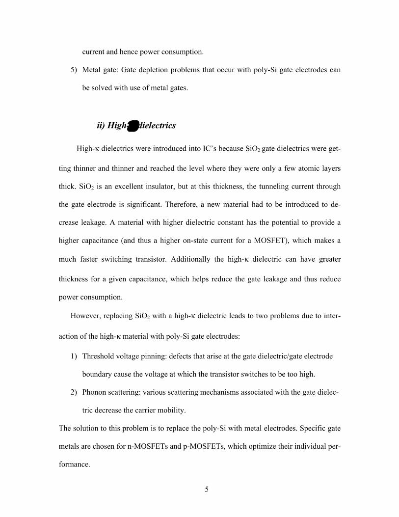
The equivalent oxide thickness (EOT) of a high-κ dielectric is defined as the thick-
ness of the SiO2 that provides the same capacitance as the high-κ dielectric.
�
tEOT = thigh−kκ SiO2
κ high−k
(1)
An example of how high-κ material helps reduce EOT is shown in Fig. 1.3. High-κ mate-
rial with greater physical thickness can provide a lower EOT than a SiO2 film.
The degradation of carrier mobility in the inversion layer in MOSFETs with high-κ
dielectrics is an area of active research. The high-κ – silicon interface is not as smooth as
the SiO2-silicon interface. Thus the interface and border trap densities are usually high for
the high-κ – silicon interface. This results in degraded carrier mobility in the inversion
layer [6].
Fig. 1.3. a) Traditional MOS structure with Gate, SiO2 as gate dielectric, and silicon substrate. b) MOS structure with high-κ material as gate dielectric. (image courtesy of Intel Corp.)
7
iii) Alternative Substrate MOSFETs
A) Ge p-MOSFETs
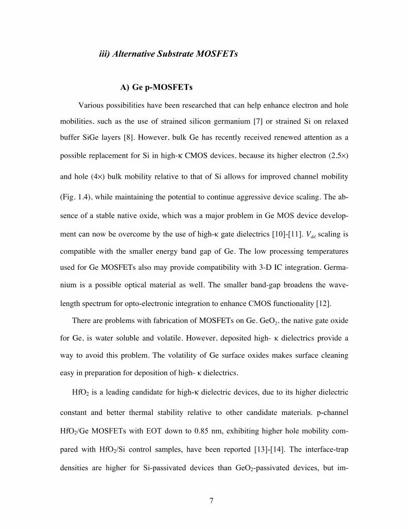
Various possibilities have been researched that can help enhance electron and hole
mobilities, such as the use of strained silicon germanium [7] or strained Si on relaxed
buffer SiGe layers [8]. However, bulk Ge has recently received renewed attention as a
possible replacement for Si in high-κ CMOS devices, because its higher electron (2.5×)
and hole (4×) bulk mobility relative to that of Si allows for improved channel mobility
(Fig. 1.4), while maintaining the potential to continue aggressive device scaling. The ab-
sence of a stable native oxide, which was a major problem in Ge MOS device develop-
ment can now be overcome by the use of high-κ gate dielectrics [10]-[11]. Vdd scaling is
compatible with the smaller energy band gap of Ge. The low processing temperatures
used for Ge MOSFETs also may provide compatibility with 3-D IC integration. Germa-
nium is a possible optical material as well. The smaller band-gap broadens the wave-
length spectrum for opto-electronic integration to enhance CMOS functionality [12].
There are problems with fabrication of MOSFETs on Ge. GeO2, the native gate oxide
for Ge, is water soluble and volatile. However, deposited high- κ dielectrics provide a
way to avoid this problem. The volatility of Ge surface oxides makes surface cleaning
easy in preparation for deposition of high- κ dielectrics.
HfO2 is a leading candidate for high-κ dielectric devices, due to its higher dielectric
constant and better thermal stability relative to other candidate materials. p-channel
HfO2/Ge MOSFETs with EOT down to 0.85 nm, exhibiting higher hole mobility com-
pared with HfO2/Si control samples, have been reported [13]-[14]. The interface-trap
densities are higher for Si-passivated devices than GeO2-passivated devices, but im-
8
proved process control is achieved with the Si-passivated devices. The trap density is
asymmetric in the band gap with a higher trap density (of the order of 1013 cm-2 eV-1)
near the conduction band and a lower trap density (of the order of 1012 cm-2 eV-1) near the
valence band [15].
B) III-V n-MOSFETs
Significant improvements have been made in MOSFET performance by combining
indium (In) rich InGaAs channels with high-κ dielectrics grown by atomic layer deposi-
tion. This suggests that In-rich InGaAs would be an excellent channel material for n-
MOSFETs. It can provide higher effective electron mobility, higher saturation velocity,
and large on-state current, and still has a sufficiently wide enough band-gap for high-
speed low-power logic applications [16]. Research on III-V MOSFETs began in 1965
when the Radio Corporation of America announced that it built the first GaAs MOSFET
[17]. Even after decades of research, III-V MOSFETs were not able to provide higher
drive currents than their Si counterparts. However, we have now entered the fifth era of
Fig. 1.4. Comparison of carrier drift velocities of Si, Ge and GaAs [9].
9
advancement for alternative-substrate MOSFETs. These could include germanium, III-
Vs, carbon nanotubes and possibly graphene [18].
Phosphides are also suitable for logic applications, whereas GaN-based MOSFETs
could potentially improve the output power, dynamic swing and reliability for RF power
applications. Meanwhile, GaAs-based MOSFETs promise to deliver higher mobilities
and higher breakdown voltages than the silicon LDMOSFETs that are currently being
employed in wireless base stations.
iv) SiC power MOS devices
Silicon carbide (SiC) is another material system that has gained significant interest
recently, although for a different application: power devices. Silicon carbide is a candi-
date material for high-power and high-frequency electronic devices due to its excellent
thermal conductivity and high breakdown field [19]. It is preferred over other wide band
gap semiconductors (such as GaN, AlGaN etc.) because SiO2 can be thermally grown to
form the gate oxide. In addition, SiC has excellent thermal and chemical stability, a large
saturation drift velocity and high bulk electron mobility. SiC exists under stoichiometri-
cally equivalent crystalline structures called polytypes. The 4H-SiC polytype has re-
ceived more attention compared to others due to its greater band gap, combined with high
and more isotropic bulk carrier mobility. Among the other SiC polytypes, cubic silicon-
carbide (3C-SiC) is another promising candidate because of its compatibility with Si
CMOS technology.
Historically, 4H-SiC MOSFETs suffered from low inversion channel mobilities due
to extremely high interface trap densities (Dit close to the 4H-SiC conduction band-edge
10
~ 1013 cm-2 eV-1). Annealing in hydrogen, which is a key in improving the quality of the
interface in SiO2/Si, is not effective in the case of SiC. Nitridation of the SiO2/SiC inter-
face, via nitric oxide (NO) or nitrous oxide (N2O) post-oxidation annealing (POA), has
emerged as the most effective solution to reduce the pre-irradiation interface trap densi-
ties [20]-[21]. Nitridation via post-oxidation annealing in nitric-oxide (NO) results in sig-
nificant reduction of Dit, which significantly improves channel mobility. Thus, it is of in-
terest to relate the incorporation of nitrogen to the reliability of SiC-based devices.
A) Polytypes of SiC
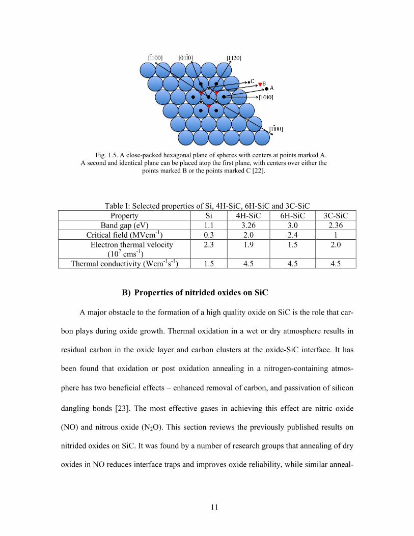
Single-crystal SiC forms in the hexagonal lattice, with alternating planes of silicon
and carbon atoms, as shown in Fig. 1.5 [22]. Each silicon atom bonds to four nearest-
neighbor carbon atoms, and each carbon atom bonds to four nearest-neighbor silicon at-
oms. As successive planes are added, each plane must be offset with respect to the plane
below. In a polytype compound, similar sheets of atoms or symmetrical variants are
stacked atop each other and related according to a symmetry operator. The differences
among the polytypes arise only in the direction perpendicular to the sheets (along the c-
axis). In SiC, each sheet represents a bilayer composed of one layer of Si atoms and one
layer of C atoms. There are a large number of possible polytypes, but the most important
are 3C, 4H, and 6H. The polytypes differ in band gap energy, carrier mobility, and break-
down field.
11
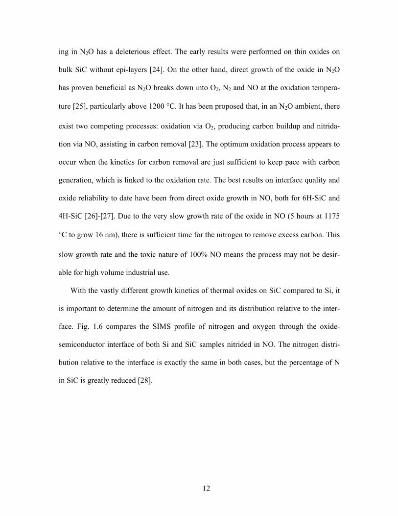
Table I: Selected properties of Si, 4H-SiC, 6H-SiC and 3C-SiC
Property Si 4H-SiC 6H-SiC 3C-SiC Band gap (eV) 1.1 3.26 3.0 2.36
Critical field (MVcm-1) 0.3 2.0 2.4 1 Electron thermal velocity
(107 cms-1) 2.3 1.9 1.5 2.0
Thermal conductivity (Wcm-1s-1) 1.5 4.5 4.5 4.5
B) Properties of nitrided oxides on SiC
A major obstacle to the formation of a high quality oxide on SiC is the role that car-
bon plays during oxide growth. Thermal oxidation in a wet or dry atmosphere results in
residual carbon in the oxide layer and carbon clusters at the oxide-SiC interface. It has
been found that oxidation or post oxidation annealing in a nitrogen-containing atmos-
phere has two beneficial effects − enhanced removal of carbon, and passivation of silicon
dangling bonds [23]. The most effective gases in achieving this effect are nitric oxide
(NO) and nitrous oxide (N2O). This section reviews the previously published results on
nitrided oxides on SiC. It was found by a number of research groups that annealing of dry
oxides in NO reduces interface traps and improves oxide reliability, while similar anneal-
Fig. 1.5. A close-packed hexagonal plane of spheres with centers at points marked A.
A second and identical plane can be placed atop the first plane, with centers over either the points marked B or the points marked C [22].
12
ing in N2O has a deleterious effect. The early results were performed on thin oxides on
bulk SiC without epi-layers [24]. On the other hand, direct growth of the oxide in N2O
has proven beneficial as N2O breaks down into O2, N2 and NO at the oxidation tempera-
ture [25], particularly above 1200 °C. It has been proposed that, in an N2O ambient, there
exist two competing processes: oxidation via O2, producing carbon buildup and nitrida-
tion via NO, assisting in carbon removal [23]. The optimum oxidation process appears to
occur when the kinetics for carbon removal are just sufficient to keep pace with carbon
generation, which is linked to the oxidation rate. The best results on interface quality and
oxide reliability to date have been from direct oxide growth in NO, both for 6H-SiC and
4H-SiC [26]-[27]. Due to the very slow growth rate of the oxide in NO (5 hours at 1175
°C to grow 16 nm), there is sufficient time for the nitrogen to remove excess carbon. This
slow growth rate and the toxic nature of 100% NO means the process may not be desir-
able for high volume industrial use.
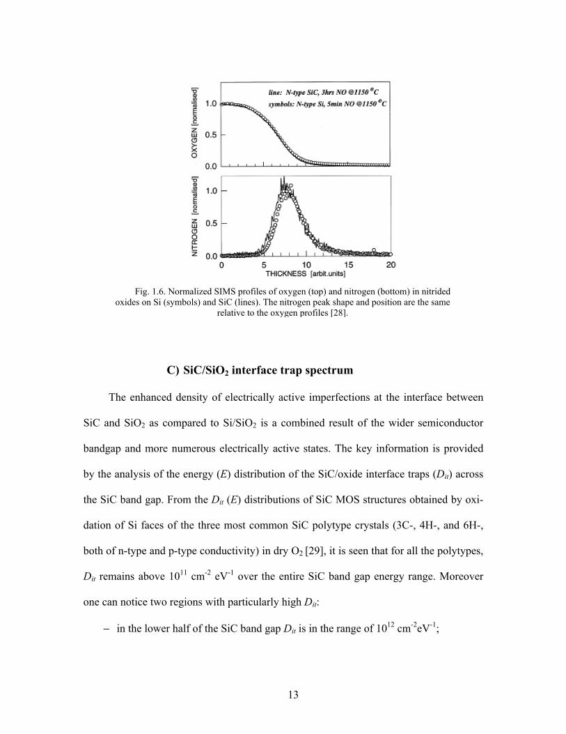
With the vastly different growth kinetics of thermal oxides on SiC compared to Si, it
is important to determine the amount of nitrogen and its distribution relative to the inter-
face. Fig. 1.6 compares the SIMS profile of nitrogen and oxygen through the oxide-
semiconductor interface of both Si and SiC samples nitrided in NO. The nitrogen distri-
bution relative to the interface is exactly the same in both cases, but the percentage of N
in SiC is greatly reduced [28].
13
C) SiC/SiO2 interface trap spectrum
The enhanced density of electrically active imperfections at the interface between
SiC and SiO2 as compared to Si/SiO2 is a combined result of the wider semiconductor
bandgap and more numerous electrically active states. The key information is provided
by the analysis of the energy (E) distribution of the SiC/oxide interface traps (Dit) across
the SiC band gap. From the Dit (E) distributions of SiC MOS structures obtained by oxi-
dation of Si faces of the three most common SiC polytype crystals (3C-, 4H-, and 6H-,
both of n-type and p-type conductivity) in dry O2 [29], it is seen that for all the polytypes,
Dit remains above 1011 cm-2 eV-1 over the entire SiC band gap energy range. Moreover
one can notice two regions with particularly high Dit:
− in the lower half of the SiC band gap Dit is in the range of 1012 cm-2eV-1;
Fig. 1.6. Normalized SIMS profiles of oxygen (top) and nitrogen (bottom) in nitrided
oxides on Si (symbols) and SiC (lines). The nitrogen peak shape and position are the same relative to the oxygen profiles [28].
14
− in the vicinity of the conduction band edge, particularly in 4H-SiC, Dit approaches
1013 cm-2eV-1.
Interface-trap density depends on the SiC polytypes used in the fabrication of MOS
capacitors. It is also sensitive to the crystallographic orientation of the SiC surface. The
general trend is the occurrence of a higher density of traps and charges at the C-face of
hexagonal SiC (6H-, 4H-polytypes) than at the Si-face [30]. Dit also increases with in-
creasing crystal surface misalignment angle from the (0001) plane (Si face), which is ex-
plained by a higher defect density at the SiC surfaces with orientations different from
(0001) [31]. In an attempt to reduce the interface trap density, numerous annealing stud-
ies were performed during the last decade. They can be divided in three groups on the
basis of the chemical mechanism behind the particular thermal treatment.
• Conventional Si technology post-oxidation anneal (POA) in non-oxidizing ambient
was applied to SiC/SiO2 samples to reduce the fixed charge density. In n-type 6H-SiC
samples the high-temperature POA in Ar is reported to improve the interface quality
significantly [32].
• Attempts to passivate defects in 6H- and 4H-SiC/SiO2 samples by attaching hydrogen
to them have shown that only weak improvement can be achieved by POA in H2 at
temperatures typical for Si (350-450 °C). With increasing temperature of the hydro-
gen anneal up to 1000 °C, a limited Dit reduction is observed in the n-type 6H- and
4H-SiC/SiO2 [34], but not in the p-type samples.
• A third group of treatments concerns direct growth or POA nitridation of oxide in ni-
tric gases (NO, N2O, NH3). In contrast to other POA treatments, nitridation allows re-
15
duction of Dit both in the upper and lower parts of the 4H-SiC band gap, albeit to a
different extent [35].
v) Conclusions
MOS devices fabricated on alternative substrate materials, namely Ge, III-V, and
SiC, have been reported in the literature. Ge and III-V substrates are important for inte-
grated circuits, whereas SiC is interesting for power MOSFETs. This chapter lays the
foundation for the research on reliability of Ge and SiC MOS done in this work.
16
CHAPTER II
BASICS OF TOTAL DOSE RADIATION AND BIAS
TEMPERATURE INSTABILITY
i) Radiation damage
Various system environments (e.g., space, nuclear reactors, etc.) can lead to radia-
tion-induced degradation of electronic components. Thus it is important to understand the
mechanisms responsible for degradation of electronic components. Many times, commer-
cial off-the-shelf (COTS) parts are used in space systems because of economic considera-
tions and ease of availability. It is extremely important to understand the underlying
physics of degradation of these commercial devices. Radiation effects on semiconductor
devices can be classified into 3 main categories:
1) Ionizing damage
2) Displacement damage
3) Single event effects
Ionizing radiation creates electron/hole pairs in the materials of interest. This radiation
may be in the form of photons with energies greater than the band-gap of the material of
concern, or in the form of particles such as electrons, protons, or atomic ions. Other
forms of radiation damage include displacement damage from particles such as protons,
neutrons, or heavy ions. Displacement damage primarily causes a reduction in minority
carrier lifetime in the silicon substrate; for example, this can have an adverse effect on the
gain of bipolar devices. Single event effects are produced by the interaction of a single
energetic particle with a sensitive device region.
17
The following radiation sources are used in this work:
1) X-ray source
In this work, an ARACOR 4100 (Advanced Research and Applications CORpora-
tion) irradiation system is used as the source of x-rays to irradiate the devices. It gener-
ates 10 keV x-rays produced by a 60 kV, 3 kW x-ray tube. A collimator and shutter sys-
tem provides a uniform 3-cm-diameter beam. The system has a radiation-tight and inter-
locked enclosure that provides safety to the operator during the exposure of the samples.
A calibrated Si PIN diode is mounted at the sample platform level to measure the dose
rate at the front surface. The dose rate can be controlled by changing the voltage and/or
current setting in the XRG 3100 x-ray generator from Philips. The voltage can be
changed in the range of 20 kV to 45 kV and the current can be changed in the range of
0.5 mA to 40 mA. In normal operation, the x-ray beam passes through 150 µm of Al fil-
tering before exposing the sample to shield the low energy portion of the x-ray spectrum.
2) Van de Graaff proton accelerator
Particle accelerators are devices used for increasing the velocity of ions and suba-
tomic particles such as protons, electrons, and positrons. The Van de Graaff accelerator
consists of a tall metal cylinder with a hollow metal dome at its top. A silk conveyor belt
runs through the middle of the cylinder. At the bottom of the cylinder, the belt collects
positive charges from a high-voltage source. The positive charges ride to the top of the
cylinder on the belt and are deposited on the outside of the dome at the top of the ma-
chine. The longer the belt runs, the more positive charges accumulate on the dome. At
some point, the accumulation of charges on the hollow dome becomes so great that a bolt
18
of lightning jumps from the dome to a metal rod near the machine. The bolt of lightning
consists of positive charges that accumulate on the dome and are finally repelled from it.
The Van de Graaff accelerator can be converted to a particle accelerator simply by attach-
ing some kind of target to the metal rod near the machine. When the bolt of lightning
strikes the metal rod, it bombards the target. The atoms of which the target is made will
be broken apart by the beam of positively charged electricity.
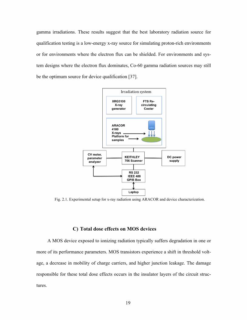
A) Experimental setup for x-ray radiation
The schematic diagram of the experimental setup for x-ray radiation is shown in
Fig. 2.1. Devices are placed on the chuck in the ARACOR 4100 x-ray source. The de-
vices can be connected to the Keithley 706 scanner, which in turn is connected to a power
supply, parameter analyzer, or LCR meter and GPIB box. Commands may be sent from
the GPIB box to switch between different devices.
B) Optimum lab source for radiation testing
Finding an optimum laboratory radiation source for testing of electron devices has
been an area of active research [36]-[37]. Both laboratory Co-60 gamma and x-ray
sources have been used to evaluate the radiation-hardness of electronic devices for space
environments.
X-ray sources can operate at higher dose rates than most Co-60 gamma sources and
can be used to irradiate individual die at the wafer level. Because of these properties, x-
ray sources are often used for process development and control [38]. It was shown that x-
ray irradiations more closely match proton radiation-induced degradation than Co-60
19
gamma irradiations. These results suggest that the best laboratory radiation source for
qualification testing is a low-energy x-ray source for simulating proton-rich environments
or for environments where the electron flux can be shielded. For environments and sys-
tem designs where the electron flux dominates, Co-60 gamma radiation sources may still
be the optimum source for device qualification [37].
C) Total dose effects on MOS devices
A MOS device exposed to ionizing radiation typically suffers degradation in one or
more of its performance parameters. MOS transistors experience a shift in threshold volt-
age, a decrease in mobility of charge carriers, and higher junction leakage. The damage
responsible for these total dose effects occurs in the insulator layers of the circuit struc-
tures.
Fig. 2.1. Experimental setup for x-ray radiation using ARACOR and device characterization.
20
The radiation damage in the oxide layers consists of three components:
1) The buildup of trapped charge in the oxide
2) An increase in the number of interface traps
3) An increase in the number of bulk oxide traps.
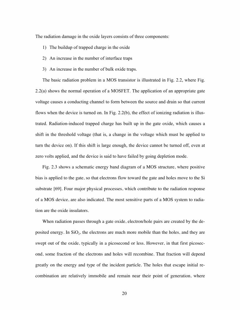
The basic radiation problem in a MOS transistor is illustrated in Fig. 2.2, where Fig.
2.2(a) shows the normal operation of a MOSFET. The application of an appropriate gate
voltage causes a conducting channel to form between the source and drain so that current
flows when the device is turned on. In Fig. 2.2(b), the effect of ionizing radiation is illus-
trated. Radiation-induced trapped charge has built up in the gate oxide, which causes a
shift in the threshold voltage (that is, a change in the voltage which must be applied to
turn the device on). If this shift is large enough, the device cannot be turned off, even at
zero volts applied, and the device is said to have failed by going depletion mode.
Fig. 2.3 shows a schematic energy band diagram of a MOS structure, where positive
bias is applied to the gate, so that electrons flow toward the gate and holes move to the Si
substrate [69]. Four major physical processes, which contribute to the radiation response
of a MOS device, are also indicated. The most sensitive parts of a MOS system to radia-
tion are the oxide insulators.
When radiation passes through a gate oxide, electron/hole pairs are created by the de-
posited energy. In SiO2, the electrons are much more mobile than the holes, and they are
swept out of the oxide, typically in a picosecond or less. However, in that first picosec-
ond, some fraction of the electrons and holes will recombine. That fraction will depend
greatly on the energy and type of the incident particle. The holes that escape initial re-
combination are relatively immobile and remain near their point of generation, where
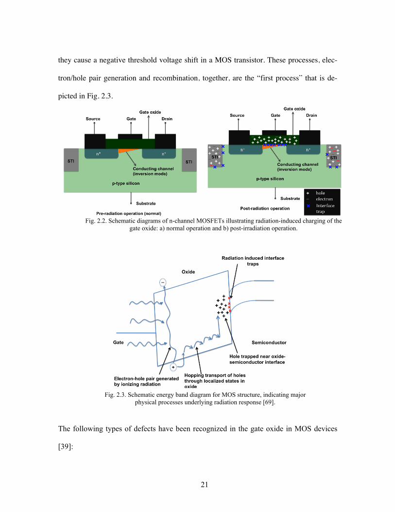
21
they cause a negative threshold voltage shift in a MOS transistor. These processes, elec-
tron/hole pair generation and recombination, together, are the “first process” that is de-
picted in Fig. 2.3.
The following types of defects have been recognized in the gate oxide in MOS devices
[39]:
Fig. 2.3. Schematic energy band diagram for MOS structure, indicating major
physical processes underlying radiation response [69].
Fig. 2.2. Schematic diagrams of n-channel MOSFETs illustrating radiation-induced charging of the
gate oxide: a) normal operation and b) post-irradiation operation.
22
1) fixed oxide charge
2) mobile ionic charge
3) interface traps
4) oxide-trap charge
5) border traps
Oxide traps and fixed oxide charge lie within the oxide, and do not communicate with
the Si [39]. Oxide trap charge is net positive charge due to trapped holes. It causes nega-
tive threshold-voltage shifts in MOSFETs and can affect the leakage current. These posi-
tive charges may be neutralized with time after radiation. Mobile ionic charges are Na+
and K+ ions that may be present in gate oxides due to human contamination. They were
of significant concern two decades back, but with innovation in extremely clean fabrica-
tion facilities, these are not much of concern in state-of-the-art MOSFETs.
Interface traps are present at the oxide-semiconductor interface and can communicate
with the semiconductor. They can trap both electrons and holes. Interface traps have been
associated with Pb centers, which are trivalent Si defects at the Si/SiO2 interface [40]. In-
terface traps build up slowly following radiation. Also radiation-induced oxide-trapped
charge has been associated with E' centers, which are trivalent Si defects in SiO2 [40].
Border traps are near-interfacial oxide traps that communicate with the Si [41]. Only
studies of defect microstructure, e.g., via electron-spin-resonance, allow clear discrimina-
tion between interface traps and border traps. It is difficult to draw a clear distinction be-
tween oxide traps and border traps, as there is no particular distance where we can say
that the oxide trap does not communicate with the semiconductor. MOS capacitors pro-
vide a good way to determine the border trap density from hysteresis between forward
23
and reverse sweep of MOS C-V characteristics [42].
Radiation induced degradation in MOSFET characteristics:
Following are the main effects of total-dose radiation on MOSFET electrical characteris-
tics:
1) Threshold shift
2) Mobility degradation
3) Increase in junction leakage
4) Change in sub-threshold slope
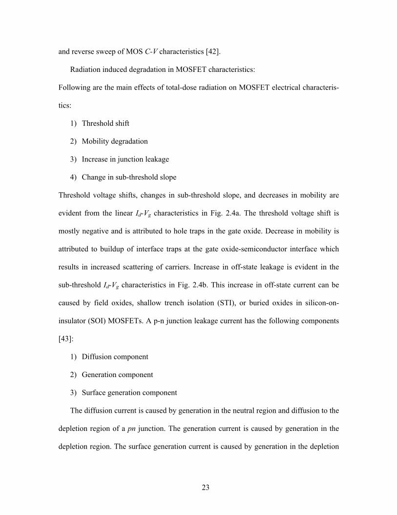
Threshold voltage shifts, changes in sub-threshold slope, and decreases in mobility are
evident from the linear Id-Vg characteristics in Fig. 2.4a. The threshold voltage shift is
mostly negative and is attributed to hole traps in the gate oxide. Decrease in mobility is
attributed to buildup of interface traps at the gate oxide-semiconductor interface which
results in increased scattering of carriers. Increase in off-state leakage is evident in the
sub-threshold Id-Vg characteristics in Fig. 2.4b. This increase in off-state current can be
caused by field oxides, shallow trench isolation (STI), or buried oxides in silicon-on-
insulator (SOI) MOSFETs. A p-n junction leakage current has the following components
[43]:
1) Diffusion component
2) Generation component
3) Surface generation component
The diffusion current is caused by generation in the neutral region and diffusion to the
depletion region of a pn junction. The generation current is caused by generation in the
depletion region. The surface generation current is caused by generation in the depletion
24
region at the Si/SiO2 interface.
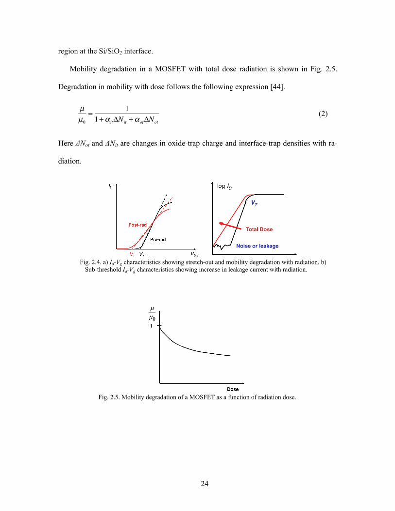
Mobility degradation in a MOSFET with total dose radiation is shown in Fig. 2.5.
Degradation in mobility with dose follows the following expression [44].
Here ΔNot and ΔNit are changes in oxide-trap charge and interface-trap densities with ra-
diation.
Fig. 2.5. Mobility degradation of a MOSFET as a function of radiation dose.
Fig. 2.4. a) Id-Vg characteristics showing stretch-out and mobility degradation with radiation. b)
Sub-threshold Id-Vg characteristics showing increase in leakage current with radiation.
�
µµ0
=1
1+ α itΔNit + αotΔNot
(2)
(1)
25
D) Total dose radiation in high-κ dielectric MOS devices
To continue improvement in device performance for a technology node, successful
efforts have been made to replace the SiO2 or nitrided SiO2 as gate dielectrics in MOS-
FETs with high-κ materials. High-κ materials such as HfO2, ZrO2, TiO2 etc. can provide
a much lower equivalent oxide thickness (EOT) than SiO2.
The effects of total dose radiation on silicon-based MOSFETs and MOS capacitors
with high-κ dielectrics such as Al2O3, HfO2 and ZrO2 have been studied before [45]-[50].
The effects of combined x-ray radiation and bias-temperature instability on high-κ MOS
capacitors have also been studied [48].
ii) Negative Bias Temperature Instability (NBTI)
Negative bias temperature instability has been known since at least 1966 [51]. It has
become an important reliability issue in sub-micron scale silicon integrated circuits. The
gate electric fields have increased as a result of scaling, IC operating temperature has in-
creased, and surface p-channel MOSFETs have replaced buried channel devices. Also,
nitrogen is routinely added to thermally grown SiO2. These factors have resulted in in-
creased degradation of MOS devices and circuits due to bias temperature stress (BTS).
A) What is NBTI?
NBTI is an increase in the absolute threshold voltage and a degradation of the mo-
bility, drain current, and transconductance of p-channel MOSFETs. It is attributed to the
creation of interface traps and oxide charge by a negative gate bias at elevated tempera-
ture. The oxide electric field is usually, but not always, lower than that leading to hot car-
26
rier degradation. The oxide electric field and temperature are similar to those typically
encountered during burn-in and sometimes encountered during high-performance chip
operation. In terms of practical impact on MOSFETs, the greatest impact of NBTI occurs
on p-MOSFETs since only those devices experience a uniform negative bias condition
during typical CMOS circuit operation.
The mechanism is ascribed to breaking of Si-H bonds at the SiO2/Si substrate inter-
face by a combination of electric field, temperature, and interactions with holes or hy-
drogenous species, resulting in dangling bonds or interface traps at that interface, desig-
nated as Dit and Nit, and positive oxide charge, Not, that may be due to H+ or trapped
holes. To simulate a NBTI condition, a negative bias is applied on the gate of a p-
MOSFET with all other terminals grounded. The wafer is heated to a constant tempera-
ture (typically 125 °C). The stress is interrupted at desired intervals for device characteri-
zation. A special technique called on-the-fly NBTI characterization allows more accurate
simulation of NBTI as the device is stressed at all times (even during characterization) in
this technique [52]. Recovery or relaxation of NBTI has also been extensively studied
recently. Under AC operating conditions, the recovery phenomenon may result in a less
severe shift in device parameters [53].
B) NBTI models
Various NBTI models have been proposed, of which the Reaction–Diffusion (R–D)
model is the most prevalent [54]-[56]. In this model, interface traps are generated at the
SiO2/Si interface (reaction) with a linear dependence on stress time. Hydrogen is released
during this reaction phase. In the subsequent diffusion phase, the hydrogen diffuses from
27
the interface into the oxide with the time dependence tn, where n for neutral hydrogen
species is frequently given as 0.25. This hydrogen diffusion results in threshold voltage
shifts ΔVT ~ tn, often attributed entirely to the generation of interface traps. While the dif-
fusion-limited regime has been verified many times, the reaction-limiting regime has not
as frequently been observed, because it occurs during a very short time. The ox-
ide/interface trap buildup also follows an exponential dependence on oxide field.
C) Interface traps and oxide charges
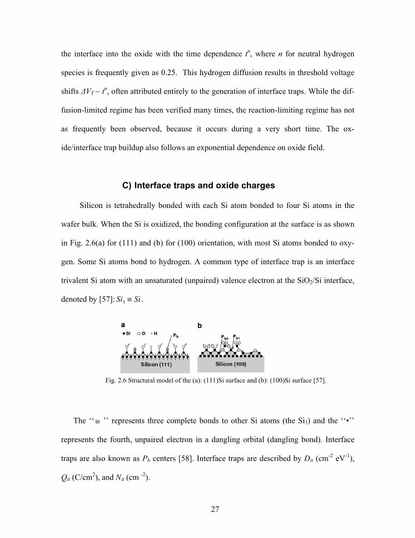
Silicon is tetrahedrally bonded with each Si atom bonded to four Si atoms in the
wafer bulk. When the Si is oxidized, the bonding configuration at the surface is as shown
in Fig. 2.6(a) for (111) and (b) for (100) orientation, with most Si atoms bonded to oxy-
gen. Some Si atoms bond to hydrogen. A common type of interface trap is an interface
trivalent Si atom with an unsaturated (unpaired) valence electron at the SiO2/Si interface,
denoted by [57]:
�
Si3 ≡ Si .
The ‘‘
�
≡ ’’ represents three complete bonds to other Si atoms (the Si3) and the ‘‘•’’
represents the fourth, unpaired electron in a dangling orbital (dangling bond). Interface
traps are also known as Pb centers [58]. Interface traps are described by Dit (cm-2 eV-1),
Qit (C/cm2), and Nit (cm -2).
Fig. 2.6 Structural model of the (a): (111)Si surface and (b): (100)Si surface [57].
28
On (111)-oriented wafers, the Pb center is a Si3
�
≡Si• center, situated at the Si/SiO2 in-
terface with its unbonded central-atom orbital perpendicular to the interface, as shown in
Fig. 2.6(a). On (100)Si, the four tetrahedral Si–Si directions intersect the interface plane
at the same angle. Two defects, named Pb1 and Pb0, have been detected by electron spin
resonance (ESR). The Pb1 center was originally thought to be a Si atom backbonded to
two substrate Si atoms, with the third saturated bond attached to an oxygen atom, desig-
nated as Si2O
�
≡Si•. This identification was found to be incorrect, as the calculated energy
levels for this defect do not agree with experiment [59]. A recent calculation suggests the
Pb1 center to be an asymmetrically oxidized dimer, with no first neighbor oxygen atoms
[60]. By 1999, it was unambiguously established that both Pb0 and Pb1 are chemically
identical to the Pb center [61]. However, there is a charge state difference between these
two centers indicating Pb0 is electrically active, while some authors believe the Pb1 to be
electrically inactive [62]. The two different effects are the result of strain relief in (100)
silicon. The defects result from the naturally occurring mismatch-induced stress at the
SiO2/Si interface during oxide growth. At room temperature and higher these two defects
contribute to the electrical activity of total interface traps [63]. Recent ESR measure-
ments show the Pb1 center to be electrically active with two distinct, narrow peaks close
to midgap in the silicon band gap [64]. However, Pb1 centers are typically generated at
densities considerably lower than Pb0 centers, making them potentially less important.
Interface traps are electrically active defects with an energy distribution throughout
the Si band gap. They act as generation/recombination centers and contribute to leakage
current, low-frequency noise, and reduced mobility, drain current, and trans-conductance.
Since electrons or holes occupy interface traps, they become charged and contribute to
29
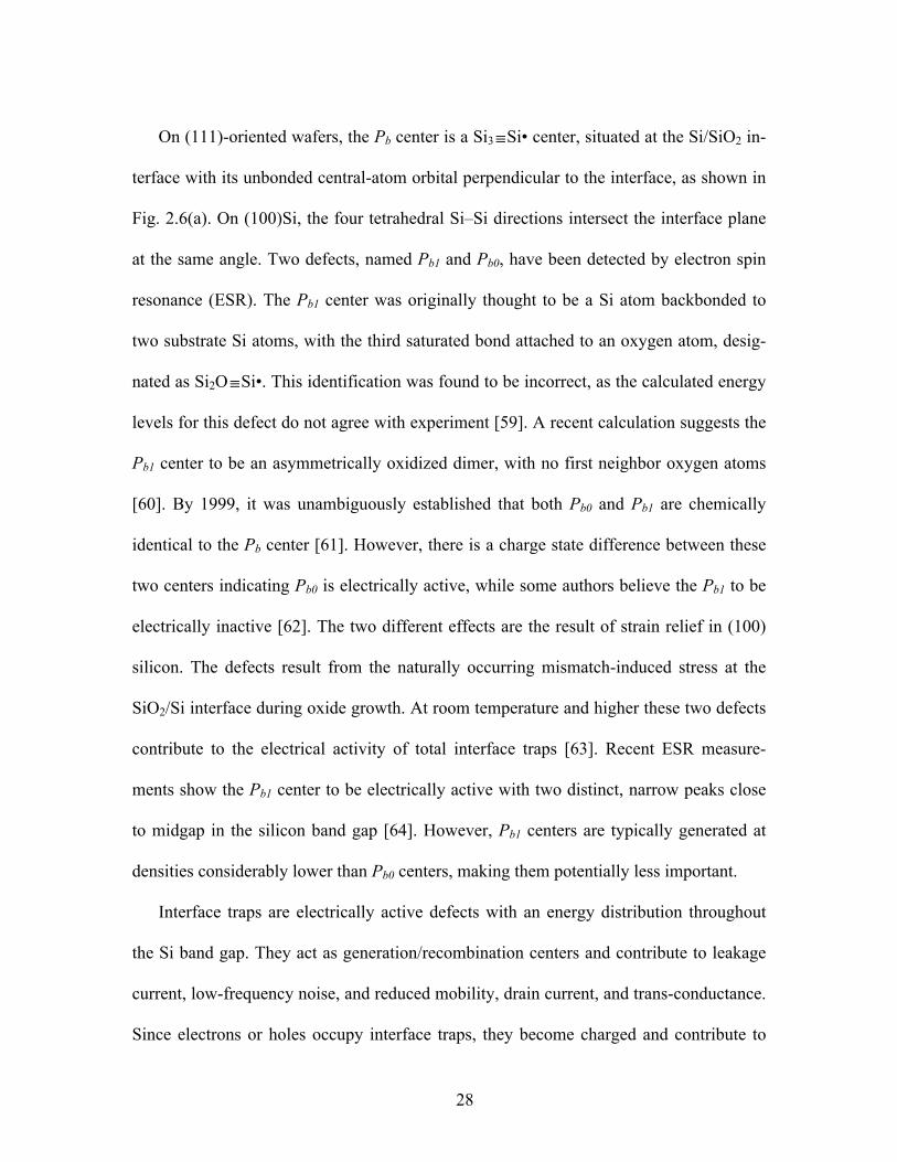
threshold voltage shifts. The surface potential dependence of the occupancy of interface
traps is illustrated in Fig. 2.7.
Interface traps at the SiO2/Si interface are acceptor-like in the upper half and donor-
like in the lower half of the band gap [65]. Hence, as shown in Fig. 2.7(a), at flatband,
with electrons occupying states below the Fermi energy, the states in the lower half of the
band gap are neutral (occupied donors designated by ‘‘0’’). Those between midgap and
the Fermi energy are negatively charged (occupied acceptors designated by “–’’), and
those above EF are neutral (unoccupied acceptors). For a p-MOSFET in inversion, shown
in Fig. 2.7(b), the interface traps between mid gap and the Fermi level are now unoccu-
pied donors, leading to positively charged interface traps (designated by ‘‘+’’). Hence
interface traps in p-channel devices in inversion are positively charged, leading to nega-
tive threshold voltage shifts. Negative bias stress generates donor states in the lower half
of the band gap [65].
The oxide charge that contributes to NBTI is not well understood. Oxide charge can
consist of various entities, including mobile charge (e.g., Na, K, and Li ions), oxide
Fig. 2.7. Band diagrams of the Si substrate of a p-channel MOS device showing the occu-
pancy of interface traps and the various charge polarities for (a) negative interface trap charge at flatband and (b) positive interface trap charge at inversion. Each of the small horizontal lines represents an interface trap. It is either occupied by an electron (solid circle) or occupied by a
hole (unoccupied by an electron), shown by the lines.
30
trapped charge (e.g., electrons and/or holes), and fixed charge. We exclude mobile
charge, because NBTI is observed when there is no mobile charge. Oxide charge is lo-
cated within the oxide and may communicate with the Si conduction and valence bands
and it is positive. Some believe the trapped charge is H+ trapped in the oxide near the
SiO2/Si interface. However, it is generally believed that hole trapping is the dominant
mechanism and that the hole traps or their precursors may exist in the insulator prior to
the stress.
The traps are positively charged when occupied by holes and neutral when unoccu-
pied. It is possible that such positively charged traps can be neutralized by electrons when
the n-substrate is at flatband and in accumulation. Similar traps have been proposed to be
responsible for low frequency (l/f) noise where electrons or holes tunnel into traps [67].
The trap distance from the SiO2/Si interface determines the tunneling time and hence the
l/f noise frequency response. Typical trap distances are 1–2 nm. The range 0.9–1.75 nm
covers the frequency range 1–104 Hz where 10 Hz corresponds to 2 nm distance. If carri-
ers can tunnel over this frequency range, this would correspond to tunnel times of 10-4–1
s, which suggests that the positive charge can be discharged in very short times, consis-
tent with NBTI experiments. Oxide charge located closer to the oxide/substrate interface
leads to higher threshold voltage shifts than charge near the gate/oxide interface. It is
rarely pointed out that charge build-up in the oxide also alters the oxide electric field.
Depending on the charges and their location, the oxide electric field may increase or de-
crease locally, e.g., near the SiO2/substrate interface.
The NBTI threshold voltage change does not depend on the hole density, determined
by changing the channel hole density and measuring the threshold voltage change. The
31
hole density can be changed by changing VT through fabrication or substrate bias. When
this was done, there was very little change in interface trap generation, indicating that
hole density is a secondary effect [68]. However, it appears that holes are required for
NBTI degradation.
The p-MOSFET threshold voltage is:
�
VT = φMS −Qot
Cox
−Qit (2φF )Cox
− 2φF −QS
Cox
(3)
where
�
φMS is the work function difference between the gate and substrate,
�
φF the Fermi
potential, Qot the positive oxide charge density (projected to the oxide-semiconductor in-
terface), QS the semiconductor charge density, and Cox the oxide capacitance/unit area. Qit
is given by
�
Qit = qDitΔE = qNit (4)
where ΔE is the energy range over which interface traps are active. Qit may be positive or
negative (Fig. 7). Since neither gate nor substrate doping density nor oxide thickness
change during stress, the threshold voltage change is due to changes in Qox and Qit as
�
ΔVT = −ΔQox + ΔQit
Cox
= −q(ΔNox + ΔNit )
Cox
(5)
where q is the electron charge, Cox is the oxide capacitance, Nit is the density of charged
interface traps, Nox is the density if oxide traps.
In today’s ICs, Nox and Nit are approximately 1010 cm-2 or slightly less before stress.
Typical ΔVT is on the order of –10 mV, leading to ΔNox + ΔNit ≈ 1011 cm-2 for tox = 2 nm,
showing the NBTI-generated charges/states are typically higher than the starting values.
How many SiH bonds are there to be dissociated? After Si oxidation, Nit = 1012–1013 cm-2
which is reduced to approximately 1010 cm-2 after low-temperature forming gas anneal-
32
ing. This suggests that ΔVT may approach –100 mV or higher after prolonged stress be-
fore the 1012–1013 cm-2 Si-H bonds are broken.
33
CHAPTER III
RADIATION EFFECTS ON GERMANIUM P-MOSFETS-
PART I: BASIC MECHANISMS
In this chapter we describe the 10 keV-x-ray radiation response of Ge p-MOSFETs
with a standard process. We consider long channel length (W/L= 9.8µm/10µm) devices.
The results of total ionizing dose irradiation on p-channel depletion mode MOSFETs
fabricated on Ge-on-Si substrates with a TiN/TaN/HfO2 gate stack are reported. There is
no significant change observed in gate leakage current, threshold voltage, or transconduc-
tance at the maximum total dose of 3 Mrad(SiO2), but there is a reduction in the on/off
current ratio of the devices as the total dose increases. This reduction is due to an increase
in drain-substrate junction leakage current, which is dominated by an increase in surface
generation current.
Total ionizing dose (TID) effects on Ge MOSFETs have not been extensively studied,
in contrast to the numerous studies of radiation effects on SiO2-based Si MOSFETs that
have been reported [69]-[70]. A few reports on TID-induced parametric degradation in
ultra thin HfO2-based Si MOSFETs are available and radiation-induced shifts in the
threshold voltage have been reported [71]. When TID effects on HfO2/Dy2O3 gate stacks
on Ge substrates were examined [72], very little degradation was reported.
This work investigates the radiation response of p-channel MOSFETs fabricated on
Ge-on-Si substrates with a TiN/TaN/HfO2 gate stack. The effects of ionizing radiation on
gate leakage currents, transconductance, on/off current ratio, and threshold voltage shift
are reported. Reduction in the on/off current ratio is identified as the most serious radia-
34
tion-effects challenge for application of these devices in ionizing radiation environments.
This reduction of on/off current ratio is primarily due to an increase in drain-substrate
junction leakage current.
i) Experimental Details
The devices studied are Ge-on-Si substrate pMOS transistors with HfO2 gate dielec-
trics. The substrates have been prepared by growing 2-µm epitaxial Ge films on Si sub-
strates by reduced pressure chemical vapor deposition (RP-CVD). The threading disloca-
tion density of the relaxed Ge epi layer is in the range of 108 cm-2. Active areas have been
defined in a SiO2 layer deposited on the Ge-on-Si substrates. The gate deposition se-
quence starts with the Ge surface passivation using a thin (4-8 monolayers�) epitaxial Si
layer that is partially oxidized. This passivation layer is immediately capped by 4 nm of
atomic layer deposited (ALD) HfO2, followed by 10 nm of TaN and 80 nm of TiN, de-
posited by physical vapor deposition (PVD). A TEM picture of the gate dielectric is
given in Fig. 3.1. The bonding arrangement at the oxide-semiconductor interface is
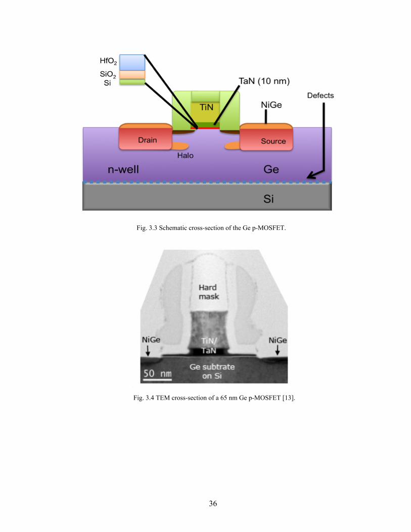
shown in Fig. 3.2. After the dry etch of the gate stack, a halo P implantation of 60 keV 4
× 1013 cm-2 was performed. The p+ regions received an extension implant of 11 keV BF2
at 8 × 1014 cm-2 and a highly doped drain (HDD) implant of 7.5 keV B to a dose of 4
×1015 cm-2, which was preceded by a Ge+ preamorphization implantation. This places the
junction at a depth of ~ 80 nm below the surface. Doping activation was conducted at 500
°C for 5 min in a nitrogen ambient environment. Self-aligned nickel germanide (NiGe)
was used for contacting the source, drain and gate. The EOT value of the gate dielectric is
1.2 nm. The W/L ratio of the devices studied is 9.8µm /10µm. The schematic diagram of
35
the device cross-section is shown in Fig. 3.3. The TEM cross-section of a 65-nm gate
length Ge p-MOSFET is shown in Fig. 3.4. The devices were exposed to 10 keV x-rays
in an ARACOR irradiator with the gate biased at 1.3 V (positive gate bias is anticipated
to be the worst bias case condition) and the other terminals grounded. The bias voltage
was applied by an HP 4156A semiconductor parameter analyzer, which also was used for
electrical characterization. The samples were irradiated to a cumulative dose of 3
Mrad(SiO2) at a dose rate of 31.5 krad(SiO2)/min. The arrangement of the MOSFETs on
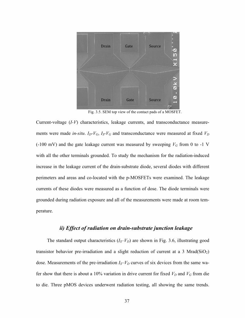
the die is shown in the SEM image in Fig. 3.5.
Fig. 3.2 shows the representation of the germanium –gate ox-
ide interface.
Fig. 3.1. TEM cross-section of the Ge p-MOSFET gate ox-
ide-semiconductor interface.
36
Fig. 3.4 TEM cross-section of a 65 nm Ge p-MOSFET [13].
Fig. 3.3 Schematic cross-section of the Ge p-MOSFET.
37
Current-voltage (I-V) characteristics, leakage currents, and transconductance measure-
ments were made in-situ. ID-VG, IS-VG and transconductance were measured at fixed VD
(-100 mV) and the gate leakage current was measured by sweeping VG from 0 to -1 V
with all the other terminals grounded. To study the mechanism for the radiation-induced
increase in the leakage current of the drain-substrate diode, several diodes with different
perimeters and areas and co-located with the p-MOSFETs were examined. The leakage
currents of these diodes were measured as a function of dose. The diode terminals were
grounded during radiation exposure and all of the measurements were made at room tem-
perature.
ii) Effect of radiation on drain-substrate junction leakage
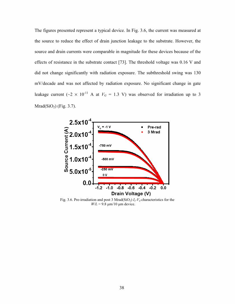
The standard output characteristics (IS–VD) are shown in Fig. 3.6, illustrating good
transistor behavior pre-irradiation and a slight reduction of current at a 3 Mrad(SiO2)
dose. Measurements of the pre-irradiation IS–VD curves of six devices from the same wa-
fer show that there is about a 10% variation in drive current for fixed VD and VG from die
to die. Three pMOS devices underwent radiation testing, all showing the same trends.
Fig. 3.5. SEM top view of the contact pads of a MOSFET.
38
The figures presented represent a typical device. In Fig. 3.6, the current was measured at
the source to reduce the effect of drain junction leakage to the substrate. However, the
source and drain currents were comparable in magnitude for these devices because of the
effects of resistance in the substrate contact [73]. The threshold voltage was 0.16 V and
did not change significantly with radiation exposure. The subthreshold swing was 130
mV/decade and was not affected by radiation exposure. No significant change in gate
leakage current (~2 × 10-11 A at VG = 1.3 V) was observed for irradiation up to 3
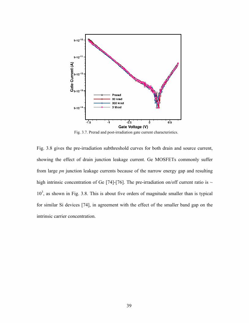
Mrad(SiO2) (Fig. 3.7).
Fig. 3.6. Pre-irradiation and post 3 Mrad(SiO2) Is-Vd characteristics for the
W/L = 9.8 µm/10 µm device.
39
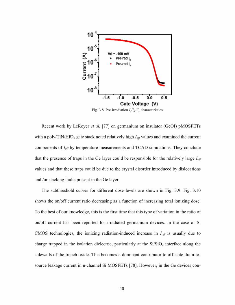
Fig. 3.8 gives the pre-irradiation subthreshold curves for both drain and source current,
showing the effect of drain junction leakage current. Ge MOSFETs commonly suffer
from large pn junction leakage currents because of the narrow energy gap and resulting
high intrinsic concentration of Ge [74]-[76]. The pre-irradiation on/off current ratio is ~
103, as shown in Fig. 3.8. This is about five orders of magnitude smaller than is typical
for similar Si devices [74], in agreement with the effect of the smaller band gap on the
intrinsic carrier concentration.
Fig. 3.7. Prerad and post-irradiation gate current characteristics.
40
Recent work by LeRoyer et al. [77] on germanium on insulator (GeOI) pMOSFETs
with a poly/TiN/HfO2 gate stack noted relatively high Ioff values and examined the current
components of Ioff by temperature measurements and TCAD simulations. They conclude
that the presence of traps in the Ge layer could be responsible for the relatively large Ioff
values and that these traps could be due to the crystal disorder introduced by dislocations
and /or stacking faults present in the Ge layer.
The subthreshold curves for different dose levels are shown in Fig. 3.9. Fig. 3.10
shows the on/off current ratio decreasing as a function of increasing total ionizing dose.
To the best of our knowledge, this is the first time that this type of variation in the ratio of
on/off current has been reported for irradiated germanium devices. In the case of Si
CMOS technologies, the ionizing radiation-induced increase in Ioff is usually due to
charge trapped in the isolation dielectric, particularly at the Si/SiO2 interface along the
sidewalls of the trench oxide. This becomes a dominant contributor to off-state drain-to-
source leakage current in n-channel Si MOSFETs [78]. However, in the Ge devices con-
Fig. 3.8. Pre-irradiation Is/Id-Vg characteristics.
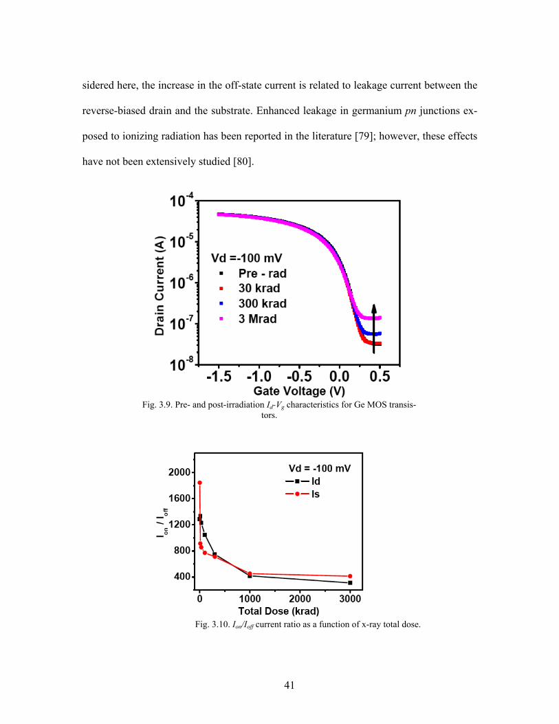
41
sidered here, the increase in the off-state current is related to leakage current between the
reverse-biased drain and the substrate. Enhanced leakage in germanium pn junctions ex-
posed to ionizing radiation has been reported in the literature [79]; however, these effects
have not been extensively studied [80].
Fig. 3.10. Ion/Ioff current ratio as a function of x-ray total dose.
Fig. 3.9. Pre- and post-irradiation Id-Vg characteristics for Ge MOS transis-
tors.
42
iii) Mechanisms that cause the increase in junction leakage with radiation
A radiation-induced increase of the pn junction leakage current can have several
causes. It is likely that the leakage current is associated with radiation damage at the iso-
lation edge, where the radiation-induced charges and interface traps can enhance the
junction peripheral leakage current. More insight may be obtained by examining the di-
ode leakage current to determine the different junction leakage current components [81].
The reverse leakage current of a pn junction consists of three major components – diffu-
sion, bulk generation, and surface generation. The first two components are proportional
to the area of the junction. The third is proportional to the perimeter of the junction. The
diffusion current is the standard (ideal) junction leakage current that saturates as the re-
verse bias increases. The bulk generation current is caused by carrier generation in the
depletion region, excluding the portion of the depletion region at the interface. Surface
generation current is caused by carrier generation where the depletion region intersects
the semiconductor-oxide interface [82].
One technique for separating the area and perimeter components relies on measuring
the reverse leakage current density of a set of diodes, identical except for different pe-
rimeter to area ratios. Measurement of the leakage current density vs. the perimeter to
area ratio should yield a straight line (see Eq.(6)). The slope represents the perimeter cur-
rent density (JP), and the intercept denotes the area component of the current density
(JA ).
JA + JP (P/A) = I/A (6)
A set of co-located diodes with different perimeter to area ratios was irradiated to
identify the dominant contribution to the reverse leakage current. The diodes were all
43
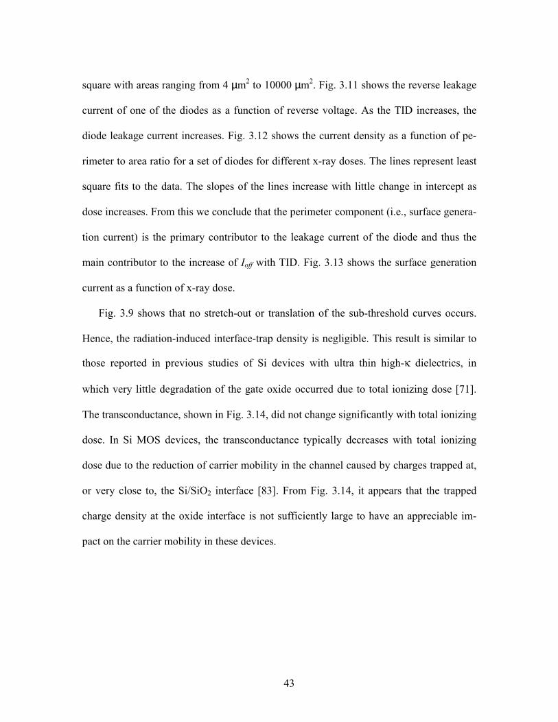
square with areas ranging from 4 µm2 to 10000 µm2. Fig. 3.11 shows the reverse leakage
current of one of the diodes as a function of reverse voltage. As the TID increases, the
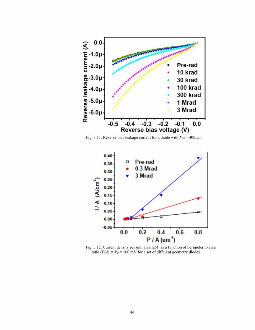
diode leakage current increases. Fig. 3.12 shows the current density as a function of pe-
rimeter to area ratio for a set of diodes for different x-ray doses. The lines represent least
square fits to the data. The slopes of the lines increase with little change in intercept as
dose increases. From this we conclude that the perimeter component (i.e., surface genera-
tion current) is the primary contributor to the leakage current of the diode and thus the
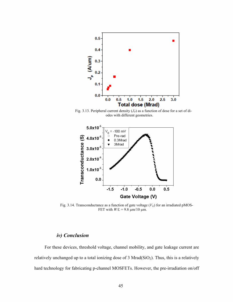
main contributor to the increase of Ioff with TID. Fig. 3.13 shows the surface generation
current as a function of x-ray dose.
Fig. 3.9 shows that no stretch-out or translation of the sub-threshold curves occurs.
Hence, the radiation-induced interface-trap density is negligible. This result is similar to
those reported in previous studies of Si devices with ultra thin high-κ dielectrics, in
which very little degradation of the gate oxide occurred due to total ionizing dose [71].
The transconductance, shown in Fig. 3.14, did not change significantly with total ionizing
dose. In Si MOS devices, the transconductance typically decreases with total ionizing
dose due to the reduction of carrier mobility in the channel caused by charges trapped at,
or very close to, the Si/SiO2 interface [83]. From Fig. 3.14, it appears that the trapped
charge density at the oxide interface is not sufficiently large to have an appreciable im-
pact on the carrier mobility in these devices.
44
Fig. 3.11. Reverse bias leakage current for a diode with P/A= 400/cm.
Fig. 3.12. Current density per unit area (I/A) as a function of perimeter to area
ratio (P/A) at VR = 100 mV for a set of different geometry diodes.
45
iv) Conclusion
For these devices, threshold voltage, channel mobility, and gate leakage current are
relatively unchanged up to a total ionizing dose of 3 Mrad(SiO2). Thus, this is a relatively
hard technology for fabricating p-channel MOSFETs. However, the pre-irradiation on/off
Fig. 3.14. Transconductance as a function of gate voltage (VG) for an irradiated pMOS-
FET with W/L = 9.8 µm/10 µm.
Fig. 3.13. Peripheral current density (JP) as a function of dose for a set of di-
odes with different geometries.
46
current ratio of ~ 103 is reduced to ~ 300 after a total dose of 3 Mrad(SiO2). The reduc-
tion in the on/off current value or increase in the off-state current of the transistor is due
to an increase in the leakage current. Potential challenges in designing circuits for radia-
tion environments using this particular Ge technology may include ability to distinguish
between on- and off-states, an increase in the off-state power dissipation, which in turn
will require an increase in the thermal budget, and possible reduction in operating time
for mobile applications.
47
CHAPTER IV
RADIATION EFFECTS ON GERMANIUM P-MOSFETS-
PART II: UNDERSTANDING EFFECT OF VARIATION IN HALO DOPING AND SI MONOLAYER THICKNESS
In this chapter we extend the study to the radiation response of Ge p-MOSFETs
with variation in Si monolayer thickness and halo doping density. We focus on devices
with relatively short channel lengths (W/L = 9.8 µm/0.5 µm).
The interface-trap densities are higher for Si-passivated devices than the GeO2-
passivated devices, but improved process control is achieved with the Si-passivated de-
vices. The trap density is asymmetric in the band gap with a higher trap density (of the
order of 1013 cm-2 eV-1) near the conduction band and a lower trap density (of the order of
1012 cm-2 eV-1) near the valence band [84].
The devices were irradiated with 10 keV x-rays. For these kinds of devices, 10-keV
x-rays can simulate the response to the high energy particles found in space applications
very well [85]. We report the radiation-induced variation of mobility, threshold voltage
(VT) shift and on/off current ratio. Reduction in the on/off current ratio is identified as the
most serious reliability issue for these devices when exposed to 10-keV x-ray radiation. It
is shown that the on-off current ratio after irradiation is greater for short channel length
devices than for long channel length devices. The reduction of on/off current ratio with x-
ray radiation is primarily due to an increase in drain-substrate junction leakage current. A
strong dependence of on-off current ratio on halo doping density is reported.
48
i) Device and experimental details
The devices studied are p-MOSFETs fabricated on Ge-on-Si epitaxial substrates,
with a relaxed 2 µm Ge layer directly deposited by Reduced Pressure Chemical Vapor
Deposition (RP-CVD), leading to a threading dislocation density (TDD) in the range of
~108 cm-2. In order to achieve a good passivation of the Ge-oxide interface, i.e., a low
Dit, several monolayers (ML) of silicon have been deposited, followed by an ozone oxi-
dation. In this paper, devices with five and eight interfacial Si monolayers are considered.
On top of the Si monolayers, hafnium oxide (HfO2) of 4 nm thickness is formed by
Atomic Layer Deposition (ALD). The gate stack is completed by 10 nm of tantalum ni-
tride (TaN) and 70 nm of titanium nitride (TiN), made by physical vapor deposition. Af-
ter the dry etch of the gate stack, a halo arsenic (As) implantation of 80 keV with varying
implant doses was performed (see Table I). The p+ regions received an extension implant
of boron or BF2 and a highly doped drain (HDD) implant of 7.5 keV boron (B) to a dose
of 4 × 1015 cm–2, which was preceded by a Ge+ pre-amorphization implantation at 550°C
in a nitrogen ambient. This places the junction at a depth of ~ 80 nm below the surface.
Self-aligned nickel germanide was used for contacting the source, drain and gate. The
EOT value of the gate dielectric is 1.2 nm. The devices studied have a W/L ratio of 9.8
µm/0.5 µm, and have source and drain areas of 74 µm2 and perimeters of 25 µm.
The irradiation was performed on wafer level devices in a 10-keV ARACOR x-ray ir-
radiator. The gate was biased at 1.3 V and the other terminals were grounded during irra-
diation. Device characterization was performed using an HP 4156A semiconductor pa-
rameter analyzer.
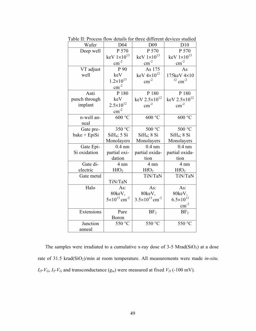
49
Table II: Process flow details for three different devices studied Wafer D04 D09 D10
Deep well P 570 keV 1×10¹³
cm-2
P 570 keV 1×10¹³
cm-2
P 570 keV 1×10¹³
cm-2 VT adjust well
P 90 keV
1.2×10¹³
cm-2
As 175 keV 4×10¹²
cm-2
As 175keV 4×10
12 cm-2
Anti punch through
implant
P 180 keV
2.5×1012 cm-2
P 180 keV 2.5×10¹²
cm-2
P 180 keV 2.5×10¹²
cm-2
n-well an-neal
600 °C 600 °C 600 °C
Gate pre-bake + EpiSi
350 °C SiH4; 5 Si
Monolayers
500 °C SiH4; 8 Si
Monolayers
500 °C SiH4; 8 Si
Monolayers Gate Epi-
Si oxidation 0.4 nm
partial oxi-dation
0.4 nm partial oxida-
tion
0.4 nm partial oxida-
tion Gate di-
electric 4 nm
HfO2 4 nm
HfO2 4 nm
HfO2 Gate metal
TiN/TaN TiN/TaN TiN/TaN
Halo As: 80keV,
5×1013 cm-2
As: 80keV,
3.5×1013 cm-2
As: 80keV,
6.5×1013 cm-2
Extensions Pure Boron
BF2 BF2
Junction anneal
550 °C
550 °C
550 °C
The samples were irradiated to a cumulative x-ray dose of 3-5 Mrad(SiO2) at a dose
rate of 31.5 krad(SiO2)/min at room temperature. All measurements were made in-situ.
ID-VG, IS-VG and transconductance (gm) were measured at fixed VD (-100 mV).
50
ii) Experimental Results
For Ge MOSFETs the off-state junction leakage current is relatively large, espe-
cially for the reverse-biased drain, due to the small Ge band gap. Good pre-irradiation
device characteristics are observed for these state of the art Ge p-MOSFETs. Fig. 4.1
shows the on-off current (Ion/Ioff) as a function of x-ray dose (in krad(SiO2)) for the three
devices considered. Device D09 with eight Si monolayers and lowest halo doping density
shows the maximum starting on-off current ratio. The on-off current ratio for all three
devices decreases with increasing dose. Device D04 and D10 have very similar starting
Ion/Ioff, but device D04 shows a more rapid fall in the ratio with increasing dose. This is
attributed to the difference in interfacial properties (five vs. eight Si monolayers). Shorter
channel length devices (W/L=9.8µm/0.5µm) show a much greater pre-irradiation Ion/Ioff
than the long channel length (W/L= 9.8µm/10µm) devices that are examined in Fig. 4.2.
This is because the on-state current is much higher for the short channel than the long
channel device for a similar magnitude off-state current. The Ion/Ioff ratio has the same
trend for short and long channel length devices for varying x-ray dose. This suggests that
the mechanism responsible for increase in junction leakage for long and short channel
device is the same.
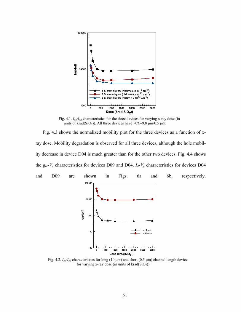
51
Fig. 4.3 shows the normalized mobility plot for the three devices as a function of x-
ray dose. Mobility degradation is observed for all three devices, although the hole mobil-
ity decrease in device D04 is much greater than for the other two devices. Fig. 4.4 shows
the gm-Vg characteristics for devices D09 and D04. Id-Vg characteristics for devices D04
and D09 are shown in Figs. 6a and 6b, respectively.
Fig. 4.2. Ion/Ioff characteristics for long (10 µm) and short (0.5 µm) channel length device
for varying x-ray dose (in units of krad(SiO2)).
Fig. 4.1. Ion/Ioff characteristics for the three devices for varying x-ray dose (in
units of krad(SiO2)). All three devices have W/L=9.8 µm/0.5 µm.
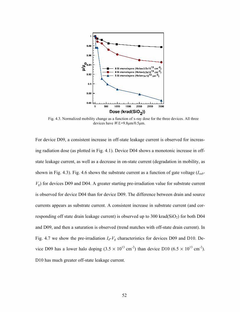
52
For device D09, a consistent increase in off-state leakage current is observed for increas-
ing radiation dose (as plotted in Fig. 4.1). Device D04 shows a monotonic increase in off-
state leakage current, as well as a decrease in on-state current (degradation in mobility, as
shown in Fig. 4.3). Fig. 4.6 shows the substrate current as a function of gate voltage (Isub-
Vg) for devices D09 and D04. A greater starting pre-irradiation value for substrate current
is observed for device D04 than for device D09. The difference between drain and source
currents appears as substrate current. A consistent increase in substrate current (and cor-
responding off state drain leakage current) is observed up to 300 krad(SiO2) for both D04
and D09, and then a saturation is observed (trend matches with off-state drain current). In
Fig. 4.7 we show the pre-irradiation Id-Vg characteristics for devices D09 and D10. De-
vice D09 has a lower halo doping (3.5 × 1013 cm-2) than device D10 (6.5 × 1013 cm-2).
D10 has much greater off-state leakage current.
Fig. 4.3. Normalized mobility change as a function of x-ray dose for the three devices. All three
devices have W/L=9.8µm/0.5µm.
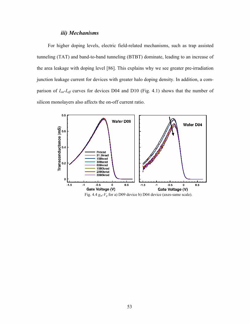
53
iii) Mechanisms
For higher doping levels, electric field-related mechanisms, such as trap assisted
tunneling (TAT) and band-to-band tunneling (BTBT) dominate, leading to an increase of
the area leakage with doping level [86]. This explains why we see greater pre-irradiation
junction leakage current for devices with greater halo doping density. In addition, a com-
parison of Ion-Ioff curves for devices D04 and D10 (Fig. 4.1) shows that the number of
silicon monolayers also affects the on-off current ratio.
Fig. 4.4 gm-Vg for a) D09 device b) D04 device (axes-same scale).
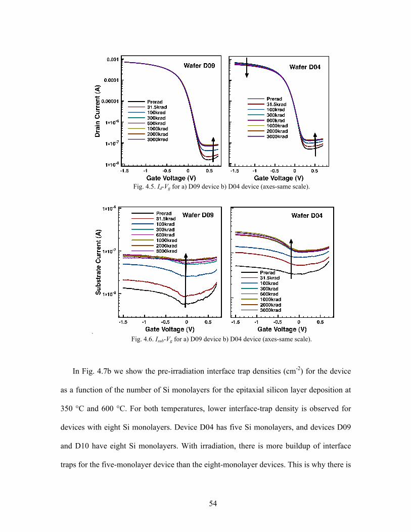
54
In Fig. 4.7b we show the pre-irradiation interface trap densities (cm-2) for the device
as a function of the number of Si monolayers for the epitaxial silicon layer deposition at
350 °C and 600 °C. For both temperatures, lower interface-trap density is observed for
devices with eight Si monolayers. Device D04 has five Si monolayers, and devices D09
and D10 have eight Si monolayers. With irradiation, there is more buildup of interface
traps for the five-monolayer device than the eight-monolayer devices. This is why there is
. Fig. 4.6. Isub-Vg for a) D09 device b) D04 device (axes-same scale).
.
Fig. 4.5. Id-Vg for a) D09 device b) D04 device (axes-same scale).
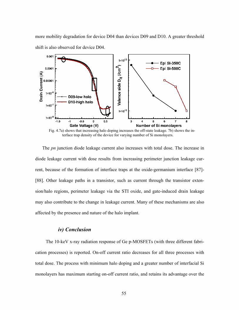
55
more mobility degradation for device D04 than devices D09 and D10. A greater threshold
shift is also observed for device D04.
The pn junction diode leakage current also increases with total dose. The increase in
diode leakage current with dose results from increasing perimeter junction leakage cur-
rent, because of the formation of interface traps at the oxide-germanium interface [87]-
[88]. Other leakage paths in a transistor, such as current through the transistor exten-
sion/halo regions, perimeter leakage via the STI oxide, and gate-induced drain leakage
may also contribute to the change in leakage current. Many of these mechanisms are also
affected by the presence and nature of the halo implant.
iv) Conclusion
The 10-keV x-ray radiation response of Ge p-MOSFETs (with three different fabri-
cation processes) is reported. On-off current ratio decreases for all three processes with
total dose. The process with minimum halo doping and a greater number of interfacial Si
monolayers has maximum starting on-off current ratio, and retains its advantage over the
Fig. 4.7a) shows that increasing halo doping increases the off-state leakage. 7b) shows the in-
terface trap density of the device for varying number of Si monolayers.
56
other devices after receiving a dose of 3 Mrad(SiO2). The devices with the fewest interfa-
cial Si monolayers show the most mobility degradation.
57
CHAPTER V
TEMPERATURE STRESS RESPONSE OF GERMA-
NIUM MOS CAPACITORS WITH HFO2/HFSION GATE
Temperature and electrical stress-induced degradation in germanium substrate MOS
capacitors with HfO2/HfSiON gate dielectrics is reported. The accumulation capacitance
decreases with temperature stress due to diffusion of germanium into the high-κ dielec-
tric. The interface trap and border trap densities decrease due to oxide growth at the ox-
ide-germanium interface.
i) Introduction
In this chapter, we demonstrate a strong process and temperature dependence of
NBTI-related degradation for Ge MOS capacitors with non-crystalline HfSiON and nano-
crystalline HfO2 (stacked on top) gate dielectrics. Many studies have previously used
germanium native dielectrics (GeO2, GeON, Ge3N4) or SiO2 as interfacial transition re-
gions (ITRs) between the Ge substrate and a high-κ dielectric to allow for a smooth inter-
face and good electrical characteristics [89]-[92]. However, the ITRs yield higher EOT
because of the low dielectric constants of these materials. Also, high-κ dielectrics such as
HfO2 and ZrO2 have high densities of intrinsic defects. Low effective oxide thickness
(EOT) with excellent leakage characteristics is demonstrated for these Ge devices (with
no interlayer) using HfSiON, which is of interest for high performance MOSFETs due to
its non-crystalline nature. However, we find that these devices can be very sensitive to
bias-temperature stress (BTS). Significant degradation in the capacitance-voltage (C-V)
58
characteristics is observed for devices exposed to negative bias at elevated temperatures.
EOT increases and interface-trap density decreases with rising temperature during BTS;
these effects are due to the diffusion of germanium into the high-κ dielectric and to the
re-growth of a thin oxide interlayer at the Ge-dielectric interface.
ii) Experimental details
Two different high-κ dielectric systems (a) HfO2/HfSiON (with 2 nm HfO2 and 3
nm HfSiON; EOT ~ 1.2 nm) and (b) HfSiON (5 nm HfSiON; EOT ~ 1.6 nm) are consid-
ered here (schematic diagrams are shown in Fig. 5.1). The MOS capacitors were fabri-
cated on n and p-Ge substrates of resistivity ~ 0.01 Ω-cm. The n-type Ge wafer was se-
quentially rinsed with de-ionized water, H2O2 6%, methanol, NH4OH 15%, and de-
ionized water again, removing the native oxide layer and producing a flat Ge surface.
Immediately following this surface treatment, the Ge wafer was introduced into the vac-
uum load lock of a remote plasma-enhanced metal-organic chemical vapor deposition
RPE-MOCVD chamber. A sacrificial, plasma-nitrided interfacial layer, and then a high-κ
oxide film were deposited by RPE-MOCVD, each at 300 °C. The sacrificial GeNx layer
had a thickness of 0.7 ± 0.1 nm and was grown in order to prevent direct reaction be-
tween the Ge substrate and the high-κ film, as well as substrate oxidation during the high-
κ film deposition process. However, this interfacial GeNx layer may also limit the attain-
able downscaling of equivalent oxide thickness because of a lower dielectric constant
than the high-κ dielectrics. As an alternative approach unique to this study, the interfacial
GeNx layer was removed by using a 1 min PDA treatment in Ar at 800 °C, which was
sufficient to dissociate Ge–N bonds in the interfacial layer [93]. Following the PDA and
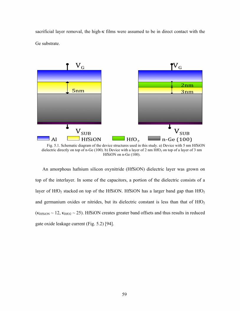
59
sacrificial layer removal, the high-κ films were assumed to be in direct contact with the
Ge substrate.
An amorphous hafnium silicon oxynitride (HfSiON) dielectric layer was grown on
top of the interlayer. In some of the capacitors, a portion of the dielectric consists of a
layer of HfO2 stacked on top of the HfSiON. HfSiON has a larger band gap than HfO2
and germanium oxides or nitrides, but its dielectric constant is less than that of HfO2
(κHfSiON ~ 12, κHfO2 ~ 25). HfSiON creates greater band offsets and thus results in reduced
gate oxide leakage current (Fig. 5.2) [94].
Fig. 5.1. Schematic diagram of the device structures used in this study. a) Device with 5 nm HfSiON
dielectric directly on top of n-Ge (100). b) Device with a layer of 2 nm HfO2 on top of a layer of 3 nm HfSiON on n-Ge (100).
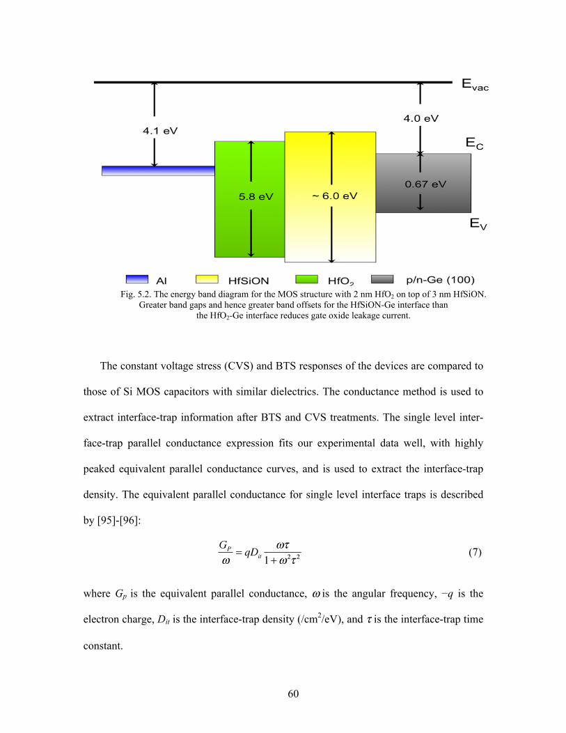
60
The constant voltage stress (CVS) and BTS responses of the devices are compared to
those of Si MOS capacitors with similar dielectrics. The conductance method is used to
extract interface-trap information after BTS and CVS treatments. The single level inter-
face-trap parallel conductance expression fits our experimental data well, with highly
peaked equivalent parallel conductance curves, and is used to extract the interface-trap
density. The equivalent parallel conductance for single level interface traps is described
by [95]-[96]:
(7)
where Gp is the equivalent parallel conductance, ω is the angular frequency, −q is the
electron charge, Dit is the interface-trap density (/cm2/eV), and τ is the interface-trap time
constant.
Fig. 5.2. The energy band diagram for the MOS structure with 2 nm HfO2 on top of 3 nm HfSiON.
Greater band gaps and hence greater band offsets for the HfSiON-Ge interface than the HfO2-Ge interface reduces gate oxide leakage current.
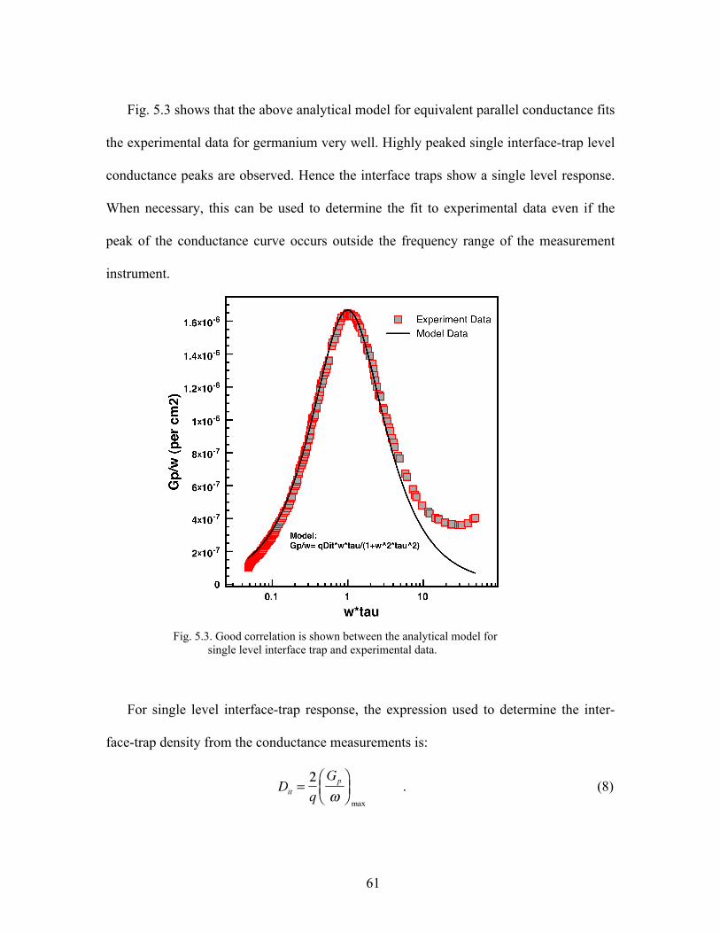
61
Fig. 5.3 shows that the above analytical model for equivalent parallel conductance fits
the experimental data for germanium very well. Highly peaked single interface-trap level
conductance peaks are observed. Hence the interface traps show a single level response.
When necessary, this can be used to determine the fit to experimental data even if the
peak of the conductance curve occurs outside the frequency range of the measurement
instrument.
For single level interface-trap response, the expression used to determine the inter-
face-trap density from the conductance measurements is:
. (8)
Fig. 5.3. Good correlation is shown between the analytical model for
single level interface trap and experimental data.
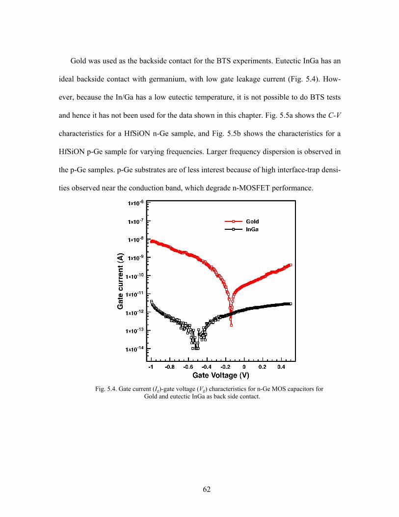
62
Gold was used as the backside contact for the BTS experiments. Eutectic InGa has an
ideal backside contact with germanium, with low gate leakage current (Fig. 5.4). How-
ever, because the In/Ga has a low eutectic temperature, it is not possible to do BTS tests
and hence it has not been used for the data shown in this chapter. Fig. 5.5a shows the C-V
characteristics for a HfSiON n-Ge sample, and Fig. 5.5b shows the characteristics for a
HfSiON p-Ge sample for varying frequencies. Larger frequency dispersion is observed in
the p-Ge samples. p-Ge substrates are of less interest because of high interface-trap densi-
ties observed near the conduction band, which degrade n-MOSFET performance.
Fig. 5.4. Gate current (Ig)-gate voltage (Vg) characteristics for n-Ge MOS capacitors for
Gold and eutectic InGa as back side contact.
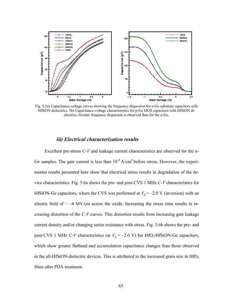
63
iii) Electrical characterization results
Excellent pre-stress C-V and leakage current characteristics are observed for the n-
Ge samples. The gate current is less than 10-4 A/cm2 before stress. However, the experi-
mental results presented here show that electrical stress results in degradation of the de-
vice characteristics. Fig. 5.6a shows the pre- and post-CVS 1 MHz C-V characteristics for
HfSiON-Ge capacitors, where the CVS was performed at Vg = –2.0 V (inversion) with an
electric field of ~ –4 MV/cm across the oxide. Increasing the stress time results in in-
creasing distortion of the C-V curves. This distortion results from increasing gate leakage
current density and/or changing series resistance with stress. Fig. 5.6b shows the pre- and
post-CVS 1 MHz C-V characteristics (at Vg = –2.0 V) for HfO2/HfSiON-Ge capacitors,
which show greater flatband and accumulation capacitance changes than those observed
in the all-HfSiON-dielectric devices. This is attributed to the increased grain size in HfO2
films after PDA treatment.
Fig. 5.5a) Capacitance-voltage curves showing the frequency dispersion for n-Ge substrate capacitors with
HfSiON dielectrics. 5b) Capacitance-voltage characteristics for p-Ge MOS capacitors with HfSiON di-electrics. Greater frequency dispersion is observed than for the n-Ge.
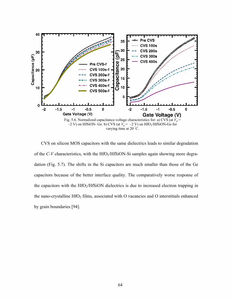
64
CVS on silicon MOS capacitors with the same dielectrics leads to similar degradation
of the C-V characteristics, with the HfO2/HfSiON-Si samples again showing more degra-
dation (Fig. 5.7). The shifts in the Si capacitors are much smaller than those of the Ge
capacitors because of the better interface quality. The comparatively worse response of
the capacitors with the HfO2/HfSiON dielectrics is due to increased electron trapping in
the nano-crystalline HfO2 films, associated with O vacancies and O interstitials enhanced
by grain boundaries [94].
Fig. 5.6. Normalized capacitance-voltage characteristics for: a) CVS (at Vg =
–2 V) on HfSiON- Ge. b) CVS (at Vg = –2 V) on HfO2/HfSiON-Ge for varying time at 20 °C.
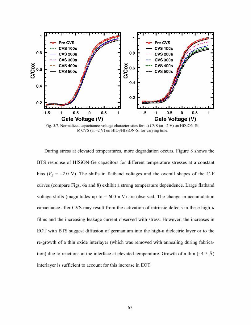
65
During stress at elevated temperatures, more degradation occurs. Figure 8 shows the
BTS response of HfSiON-Ge capacitors for different temperature stresses at a constant
bias (Vg = –2.0 V). The shifts in flatband voltages and the overall shapes of the C-V
curves (compare Figs. 6a and 8) exhibit a strong temperature dependence. Large flatband
voltage shifts (magnitudes up to ~ 600 mV) are observed. The change in accumulation
capacitance after CVS may result from the activation of intrinsic defects in these high-κ
films and the increasing leakage current observed with stress. However, the increases in
EOT with BTS suggest diffusion of germanium into the high-κ dielectric layer or to the
re-growth of a thin oxide interlayer (which was removed with annealing during fabrica-
tion) due to reactions at the interface at elevated temperature. Growth of a thin (~4-5 Å)
interlayer is sufficient to account for this increase in EOT.
Fig. 5.7. Normalized capacitance-voltage characteristics for: a) CVS (at –2 V) on HfSiON-Si;
b) CVS (at –2 V) on HfO2/HfSiON-Si for varying time.
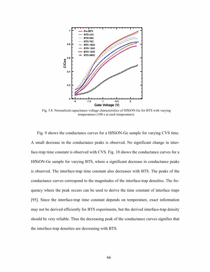
66
Fig. 9 shows the conductance curves for a HfSiON-Ge sample for varying CVS time.
A small decrease in the conductance peaks is observed. No significant change in inter-
face-trap time constant is observed with CVS. Fig. 10 shows the conductance curves for a
HfSiON-Ge sample for varying BTS, where a significant decrease in conductance peaks
is observed. The interface-trap time constant also decreases with BTS. The peaks of the
conductance curves correspond to the magnitudes of the interface-trap densities. The fre-
quency where the peak occurs can be used to derive the time constant of interface traps
[95]. Since the interface-trap time constant depends on temperature, exact information
may not be derived efficiently for BTS experiments, but the derived interface-trap density
should be very reliable. Thus the decreasing peak of the conductance curves signifies that
the interface-trap densities are decreasing with BTS.
Fig. 5.8. Normalized capacitance-voltage characteristics of HfSiON-Ge for BTS with varying
temperatures (100 s at each temperature).
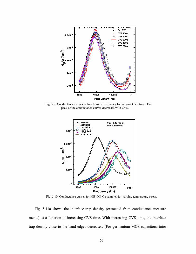
67
Fig. 5.11a shows the interface-trap density (extracted from conductance measure-
ments) as a function of increasing CVS time. With increasing CVS time, the interface-
trap density close to the band edges decreases. (For germanium MOS capacitors, inter-
Fig. 5.9. Conductance curves as functions of frequency for varying CVS time. The
peak of the conductance curves decreases with CVS.
Fig. 5.10. Conductance curves for HfSiON-Ge samples for varying temperature stress.
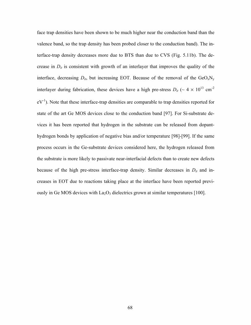
68
face trap densities have been shown to be much higher near the conduction band than the
valence band, so the trap density has been probed closer to the conduction band). The in-
terface-trap density decreases more due to BTS than due to CVS (Fig. 5.11b). The de-
crease in Dit is consistent with growth of an interlayer that improves the quality of the
interface, decreasing Dit, but increasing EOT. Because of the removal of the GeOxNy
interlayer during fabrication, these devices have a high pre-stress Dit (~ 4 × 1013 cm-2
eV-1). Note that these interface-trap densities are comparable to trap densities reported for
state of the art Ge MOS devices close to the conduction band [97]. For Si-substrate de-
vices it has been reported that hydrogen in the substrate can be released from dopant-
hydrogen bonds by application of negative bias and/or temperature [98]-[99]. If the same
process occurs in the Ge-substrate devices considered here, the hydrogen released from
the substrate is more likely to passivate near-interfacial defects than to create new defects
because of the high pre-stress interface-trap density. Similar decreases in Dit and in-
creases in EOT due to reactions taking place at the interface have been reported previ-
ously in Ge MOS devices with La2O3 dielectrics grown at similar temperatures [100].
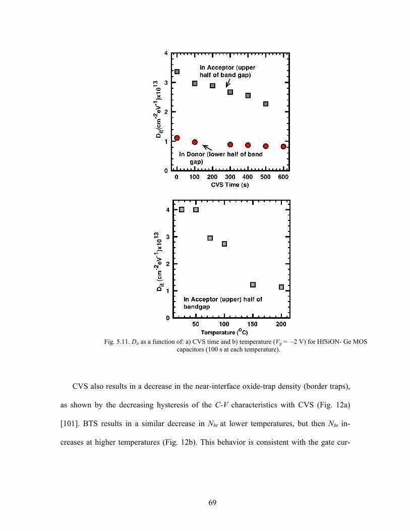
69
CVS also results in a decrease in the near-interface oxide-trap density (border traps),
as shown by the decreasing hysteresis of the C-V characteristics with CVS (Fig. 12a)
[101]. BTS results in a similar decrease in Nbt at lower temperatures, but then Nbt in-
creases at higher temperatures (Fig. 12b). This behavior is consistent with the gate cur-
Fig. 5.11. Dit as a function of: a) CVS time and b) temperature (Vg = –2 V) for HfSiON- Ge MOS
capacitors (100 s at each temperature).
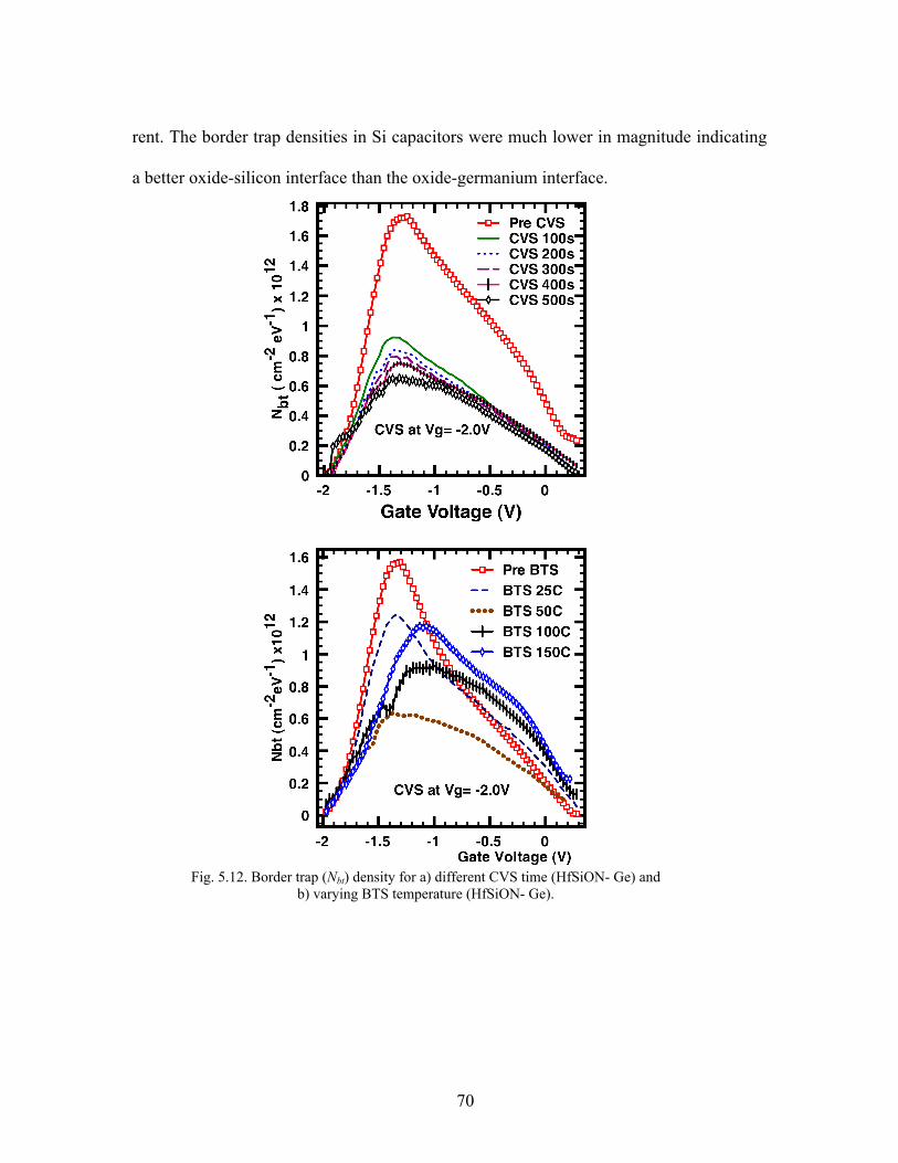
70
rent. The border trap densities in Si capacitors were much lower in magnitude indicating
a better oxide-silicon interface than the oxide-germanium interface.
Fig. 5.12. Border trap (Nbt) density for a) different CVS time (HfSiON- Ge) and
b) varying BTS temperature (HfSiON- Ge).
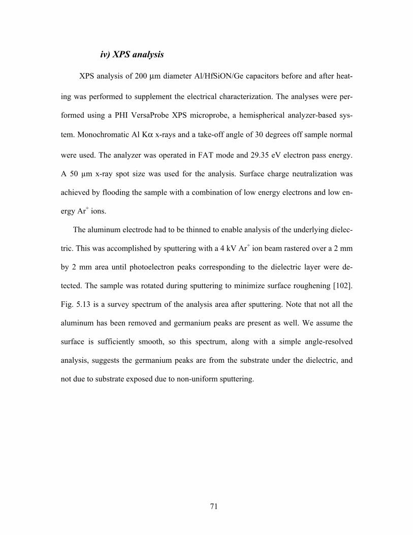
71
iv) XPS analysis
XPS analysis of 200 µm diameter Al/HfSiON/Ge capacitors before and after heat-
ing was performed to supplement the electrical characterization. The analyses were per-
formed using a PHI VersaProbe XPS microprobe, a hemispherical analyzer-based sys-
tem. Monochromatic Al Kα x-rays and a take-off angle of 30 degrees off sample normal
were used. The analyzer was operated in FAT mode and 29.35 eV electron pass energy.
A 50 µm x-ray spot size was used for the analysis. Surface charge neutralization was
achieved by flooding the sample with a combination of low energy electrons and low en-
ergy Ar+ ions.
The aluminum electrode had to be thinned to enable analysis of the underlying dielec-
tric. This was accomplished by sputtering with a 4 kV Ar+ ion beam rastered over a 2 mm
by 2 mm area until photoelectron peaks corresponding to the dielectric layer were de-
tected. The sample was rotated during sputtering to minimize surface roughening [102].
Fig. 5.13 is a survey spectrum of the analysis area after sputtering. Note that not all the
aluminum has been removed and germanium peaks are present as well. We assume the
surface is sufficiently smooth, so this spectrum, along with a simple angle-resolved
analysis, suggests the germanium peaks are from the substrate under the dielectric, and
not due to substrate exposed due to non-uniform sputtering.
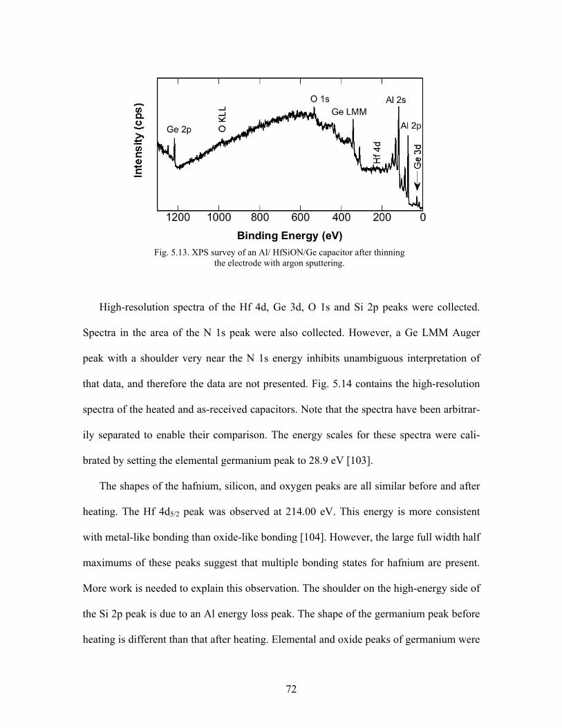
72
High-resolution spectra of the Hf 4d, Ge 3d, O 1s and Si 2p peaks were collected.
Spectra in the area of the N 1s peak were also collected. However, a Ge LMM Auger
peak with a shoulder very near the N 1s energy inhibits unambiguous interpretation of
that data, and therefore the data are not presented. Fig. 5.14 contains the high-resolution
spectra of the heated and as-received capacitors. Note that the spectra have been arbitrar-
ily separated to enable their comparison. The energy scales for these spectra were cali-
brated by setting the elemental germanium peak to 28.9 eV [103].
The shapes of the hafnium, silicon, and oxygen peaks are all similar before and after
heating. The Hf 4d5/2 peak was observed at 214.00 eV. This energy is more consistent
with metal-like bonding than oxide-like bonding [104]. However, the large full width half
maximums of these peaks suggest that multiple bonding states for hafnium are present.
More work is needed to explain this observation. The shoulder on the high-energy side of
the Si 2p peak is due to an Al energy loss peak. The shape of the germanium peak before
heating is different than that after heating. Elemental and oxide peaks of germanium were
Fig. 5.13. XPS survey of an Al/ HfSiON/Ge capacitor after thinning
the electrode with argon sputtering.
73
observed at 28.96 eV and 33.41eV, respectively. A peak suggesting the presence of ger-
manium oxide appears after heating. This supports the electrical characterization results,
suggesting an interfacial oxide layer may be formed during stressing. There is no indica-
tion of germanium diffusion in the XPS results. However, further testing using samples
more suitable to XPS analysis may be more enlightening.
Interfacial reactions due to diffusion may also account for the degradation. The rela-
tive ease with which Ge can diffuse into the HfO2 films during annealing is attributed to
the removal of the interfacial GeNx layer and the increased grain size in the HfO2 films
after the PDA treatments. Diffusion of germanium into the dielectric during PDA anneal
at higher temperatures was shown through medium energy ion scattering (MEIS) meas-
urements [105]. A similar diffusion mechanism can explain the results here.
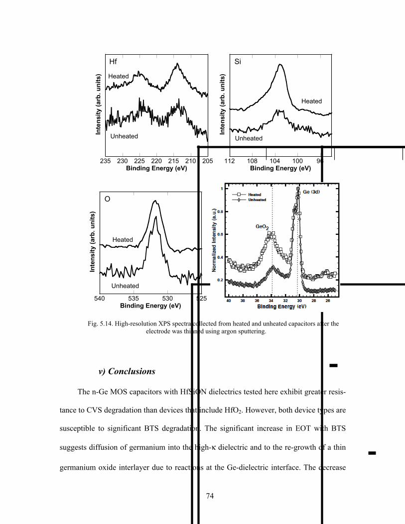
74
v) Conclusions
The n-Ge MOS capacitors with HfSiON dielectrics tested here exhibit greater resis-
tance to CVS degradation than devices that include HfO2. However, both device types are
susceptible to significant BTS degradation. The significant increase in EOT with BTS
suggests diffusion of germanium into the high-κ dielectric and to the re-growth of a thin
germanium oxide interlayer due to reactions at the Ge-dielectric interface. The decrease
205210215220225230235
Inte
nsity
(arb
. uni
ts)
Binding Energy (eV)
Heated
Unheated
Hf
96100104108112
Inte
nsity
(arb
. uni
ts)
Binding Energy (eV)
Heated
Unheated
Si
525530535540
Inte
nsity
(arb
. uni
ts)
Binding Energy (eV)
Heated
Unheated
O
Fig. 5.14. High-resolution XPS spectra collected from heated and unheated capacitors after the electrode was thinned using argon sputtering.
75
in Dit observed with CVS and BTS is consistent with the passivation of process-induced
interface traps by hydrogen released during stress and also with interlayer re-growth at
high-temperatures. While these devices are very promising because of the extremely low
effective oxide thicknesses and low leakage, it is important to understand CVS- and BTS-
related reliability issues.
76
CHAPTER VI
CHARGE TRAPPING PROPERTIES OF SIC MOS
Historically, 4H-SiC MOSFETs suffered from low inversion channel mobilities due
to extremely high pre-irradiation interface trap densities (Dit close to the 4H-SiC conduc-
tion band-edge ~ 1013 cm-2 eV-1). Annealing in hydrogen, which is a key in improving the
quality of the interface in SiO2/Si is not effective in the case of SiC. Nitridation of the
SiO2/SiC interface, via nitric oxide (NO) or nitrous oxide (N2O) post-oxidation annealing
(POA), has emerged as the most effective solution to reduce the pre-irradiation interface
trap densities [106]-[107]. Nitridation via post-oxidation annealing in nitric-oxide (NO)
results in significant reduction of Dit, which significantly improves channel mobility.
Thus, it is of interest to relate the incorporation of nitrogen to the reliability of SiC-based
devices.
3C-SiC substrate MOS capacitors with as-grown SiO2 gate dielectrics have been
shown to be very radiation tolerant [108]. The radiation response of 4H-SiC MOS capaci-
tors has also been studied recently [109]. In 4H-SiC devices, it was demonstrated that a
NO POA leads to the suppression of interface trap generation during electron injection,
but also enhances the formation of hole traps, yielding large voltage instabilities follow-
ing x-ray irradiation [110]. Here we report the total dose radiation response of both 3C-
and 4H-SiC-based MOS capacitors with either NO or N2O POA, providing a comparison
of the reliability of the SiO2/SiC interface as a function of the oxidized polytype and of
the nitridation process.
77
i) Device and Experimental details
The devices considered in this study, processed at Griffith University, are n-
substrate 3C- and 4H-SiC MOS capacitors with SiO2 as the gate dielectric thermally
grown in dry oxygen (at 1185 °C) on the silicon surface for 4H and on the (001) plane for
3C (oxide thickness in the 20-25 nm range). A schematic diagram of the device is shown
in Fig. 6.1. The starting substrates for the 4H-SiC were obtained from Cree Inc., with a
high quality SiC epitaxial layer on top. The 3C-SiC was grown on Si, and was obtained
from the Institute of Crystal Growth, Germany. The devices were exposed to NO and
N2O at 1185 °C for two and one hours, respectively. Aluminum is used as the gate and
substrate electrode. Irradiation experiments were performed with an ARACOR 10-keV x-
ray source at a dose rate of 31.5 krad(SiO2)/min. The devices were biased at different
electric fields during the radiation experiments. Constant voltage stress experiments
(CVS) were performed for the same amount of time as the device was biased during the
radiation experiments in order to separate the effects of bias and radiation on the MOS
characteristics. High frequency (1 MHz) capacitance-voltage (C-V) and conductance-
voltage (G-V) measurements were performed between successive irradiation or CVS
steps to monitor the change in the flatband voltage (Vfb). The interface-trap density be-
tween 0.2 and 0.6 eV from the SiC conduction band edge was determined from simulta-
neous high frequency and quasi-static C-V measurements made at room temperature, us-
ing the Berglund method [111].
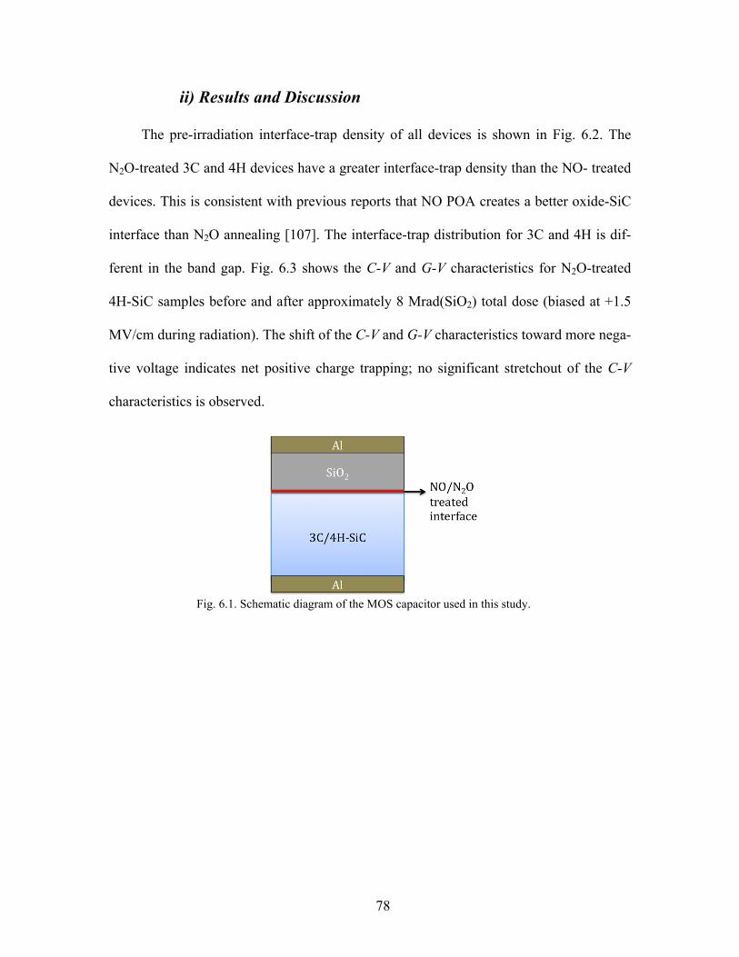
78
ii) Results and Discussion
The pre-irradiation interface-trap density of all devices is shown in Fig. 6.2. The
N2O-treated 3C and 4H devices have a greater interface-trap density than the NO- treated
devices. This is consistent with previous reports that NO POA creates a better oxide-SiC
interface than N2O annealing [107]. The interface-trap distribution for 3C and 4H is dif-
ferent in the band gap. Fig. 6.3 shows the C-V and G-V characteristics for N2O-treated
4H-SiC samples before and after approximately 8 Mrad(SiO2) total dose (biased at +1.5
MV/cm during radiation). The shift of the C-V and G-V characteristics toward more nega-
tive voltage indicates net positive charge trapping; no significant stretchout of the C-V
characteristics is observed.
Fig. 6.1. Schematic diagram of the MOS capacitor used in this study.
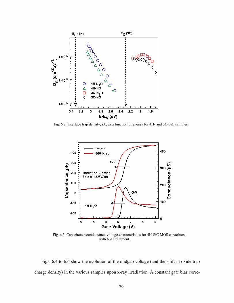
79
Figs. 6.4 to 6.6 show the evolution of the midgap voltage (and the shift in oxide trap
charge density) in the various samples upon x-ray irradiation. A constant gate bias corre-
Fig. 6.3. Capacitance/conductance-voltage characteristics for 4H-SiC MOS capacitors
with N2O treatment.
Fig. 6.2. Interface trap density, Dit, as a function of energy for 4H- and 3C-SiC samples.
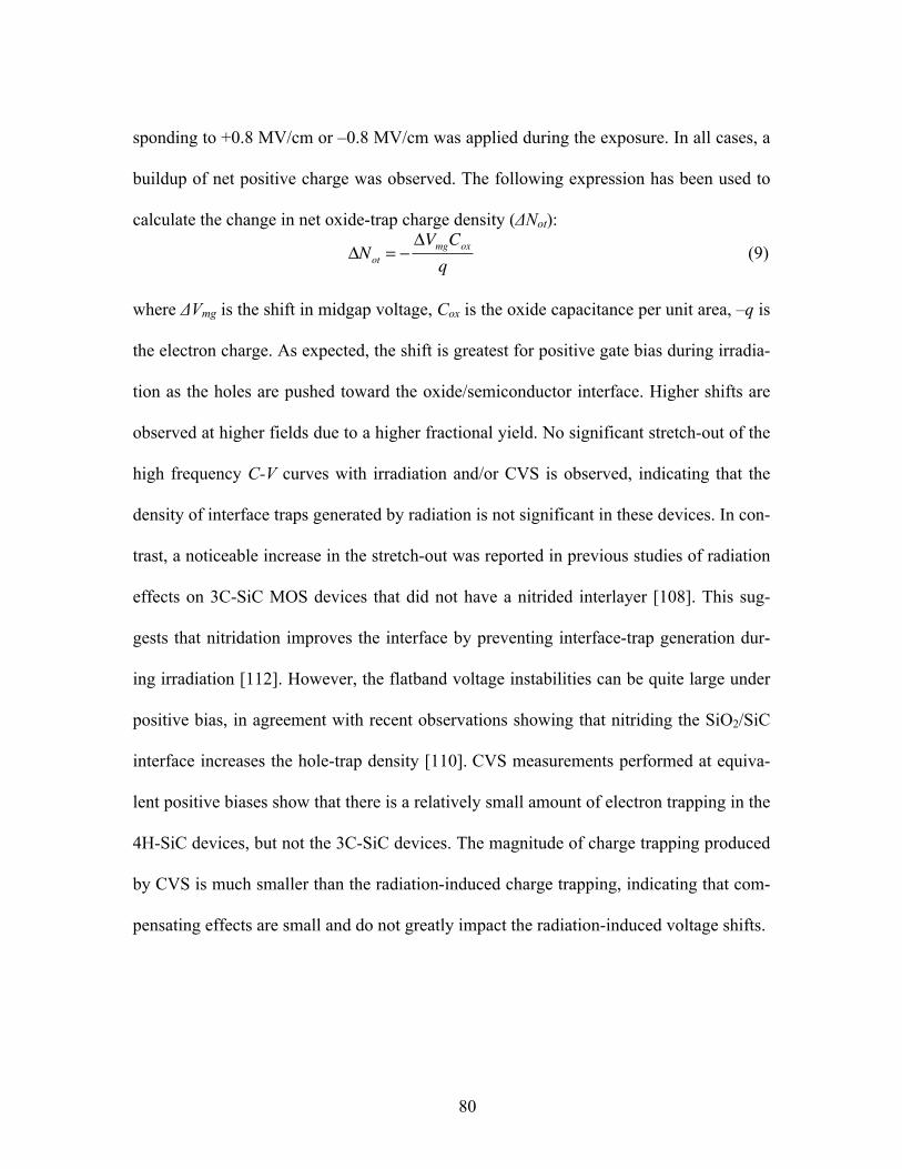
80
sponding to +0.8 MV/cm or –0.8 MV/cm was applied during the exposure. In all cases, a
buildup of net positive charge was observed. The following expression has been used to
calculate the change in net oxide-trap charge density (ΔNot):
�
ΔNot = −ΔVmgCox
q (9)
where ΔVmg is the shift in midgap voltage, Cox is the oxide capacitance per unit area, –q is
the electron charge. As expected, the shift is greatest for positive gate bias during irradia-
tion as the holes are pushed toward the oxide/semiconductor interface. Higher shifts are
observed at higher fields due to a higher fractional yield. No significant stretch-out of the
high frequency C-V curves with irradiation and/or CVS is observed, indicating that the
density of interface traps generated by radiation is not significant in these devices. In con-
trast, a noticeable increase in the stretch-out was reported in previous studies of radiation
effects on 3C-SiC MOS devices that did not have a nitrided interlayer [108]. This sug-
gests that nitridation improves the interface by preventing interface-trap generation dur-
ing irradiation [112]. However, the flatband voltage instabilities can be quite large under
positive bias, in agreement with recent observations showing that nitriding the SiO2/SiC
interface increases the hole-trap density [110]. CVS measurements performed at equiva-
lent positive biases show that there is a relatively small amount of electron trapping in the
4H-SiC devices, but not the 3C-SiC devices. The magnitude of charge trapping produced
by CVS is much smaller than the radiation-induced charge trapping, indicating that com-
pensating effects are small and do not greatly impact the radiation-induced voltage shifts.
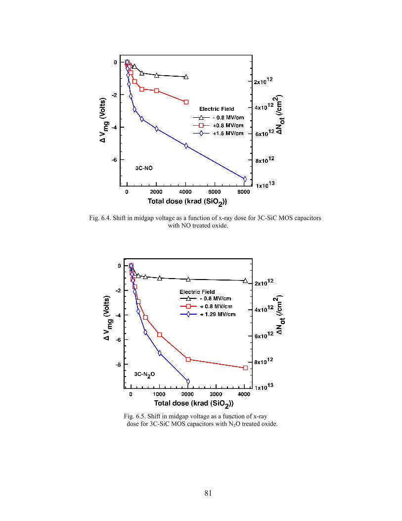
81
Fig. 6.5. Shift in midgap voltage as a function of x-ray dose for 3C-SiC MOS capacitors with N2O treated oxide.
Fig. 6.4. Shift in midgap voltage as a function of x-ray dose for 3C-SiC MOS capacitors
with NO treated oxide.
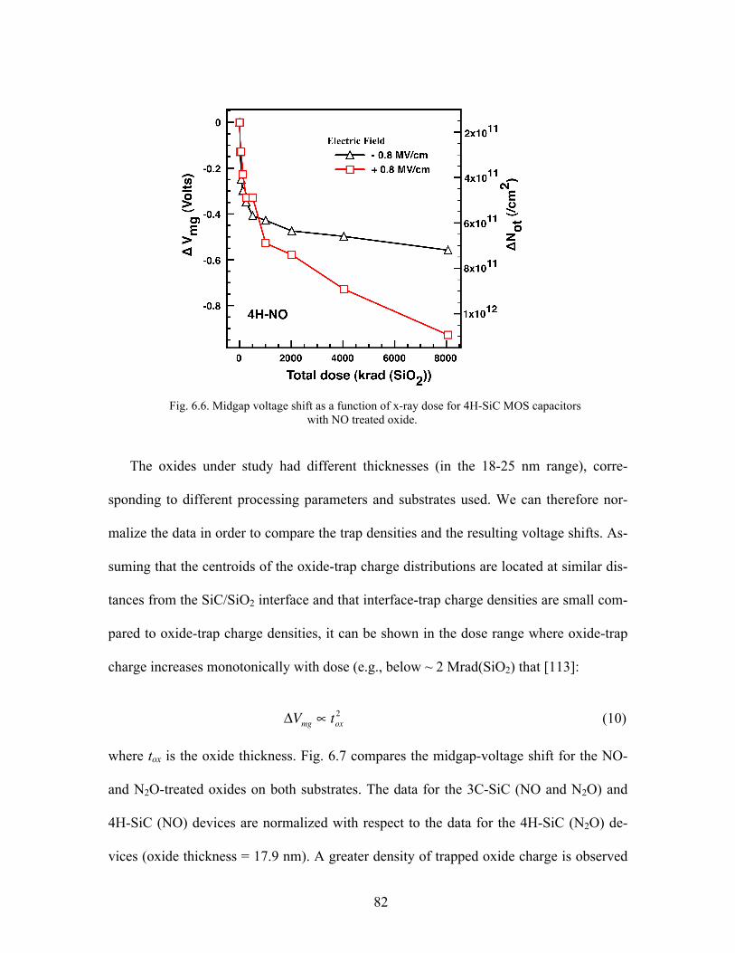
82
The oxides under study had different thicknesses (in the 18-25 nm range), corre-
sponding to different processing parameters and substrates used. We can therefore nor-
malize the data in order to compare the trap densities and the resulting voltage shifts. As-
suming that the centroids of the oxide-trap charge distributions are located at similar dis-
tances from the SiC/SiO2 interface and that interface-trap charge densities are small com-
pared to oxide-trap charge densities, it can be shown in the dose range where oxide-trap
charge increases monotonically with dose (e.g., below ~ 2 Mrad(SiO2) that [113]:
�
ΔVmg ∝ tox2 (10)
where tox is the oxide thickness. Fig. 6.7 compares the midgap-voltage shift for the NO-
and N2O-treated oxides on both substrates. The data for the 3C-SiC (NO and N2O) and
4H-SiC (NO) devices are normalized with respect to the data for the 4H-SiC (N2O) de-
vices (oxide thickness = 17.9 nm). A greater density of trapped oxide charge is observed
Fig. 6.6. Midgap voltage shift as a function of x-ray dose for 4H-SiC MOS capacitors
with NO treated oxide.
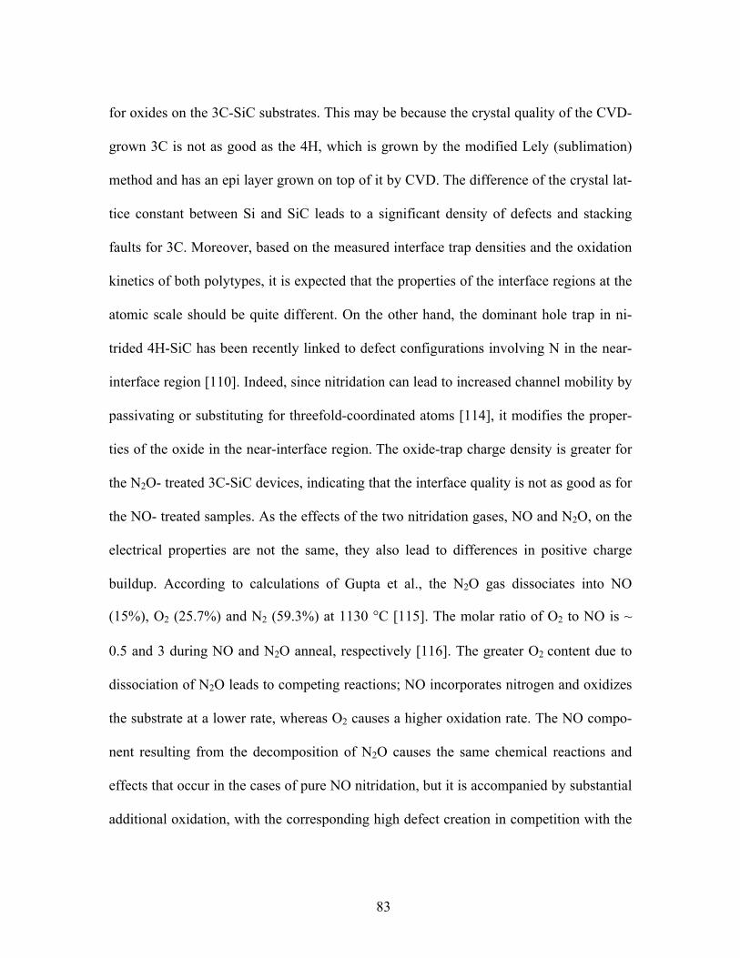
83
for oxides on the 3C-SiC substrates. This may be because the crystal quality of the CVD-
grown 3C is not as good as the 4H, which is grown by the modified Lely (sublimation)
method and has an epi layer grown on top of it by CVD. The difference of the crystal lat-
tice constant between Si and SiC leads to a significant density of defects and stacking
faults for 3C. Moreover, based on the measured interface trap densities and the oxidation
kinetics of both polytypes, it is expected that the properties of the interface regions at the
atomic scale should be quite different. On the other hand, the dominant hole trap in ni-
trided 4H-SiC has been recently linked to defect configurations involving N in the near-
interface region [110]. Indeed, since nitridation can lead to increased channel mobility by
passivating or substituting for threefold-coordinated atoms [114], it modifies the proper-
ties of the oxide in the near-interface region. The oxide-trap charge density is greater for
the N2O- treated 3C-SiC devices, indicating that the interface quality is not as good as for
the NO- treated samples. As the effects of the two nitridation gases, NO and N2O, on the
electrical properties are not the same, they also lead to differences in positive charge
buildup. According to calculations of Gupta et al., the N2O gas dissociates into NO
(15%), O2 (25.7%) and N2 (59.3%) at 1130 °C [115]. The molar ratio of O2 to NO is ~
0.5 and 3 during NO and N2O anneal, respectively [116]. The greater O2 content due to
dissociation of N2O leads to competing reactions; NO incorporates nitrogen and oxidizes
the substrate at a lower rate, whereas O2 causes a higher oxidation rate. The NO compo-
nent resulting from the decomposition of N2O causes the same chemical reactions and
effects that occur in the cases of pure NO nitridation, but it is accompanied by substantial
additional oxidation, with the corresponding high defect creation in competition with the
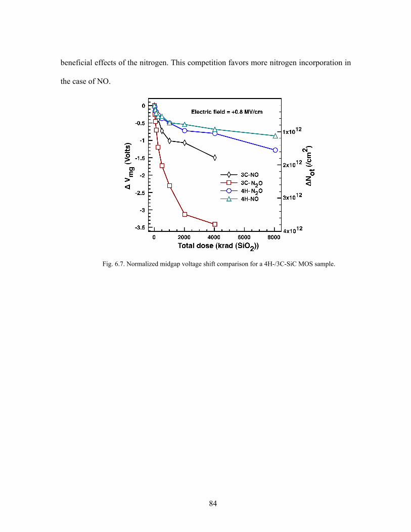
84
beneficial effects of the nitrogen. This competition favors more nitrogen incorporation in
the case of NO.
Fig. 6.7. Normalized midgap voltage shift comparison for a 4H-/3C-SiC MOS sample.
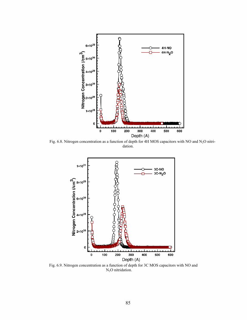
85
Fig. 6.9. Nitrogen concentration as a function of depth for 3C MOS capacitors with NO and
N2O nitridation.
Fig. 6.8. Nitrogen concentration as a function of depth for 4H MOS capacitors with NO and N2O nitri-
dation.
86
SIMS data showing the nitrogen profiles for the 3C- and 4H-SiC MOS capacitors is
shown in Fig. 6.8 and Fig. 6.9 respectively. It is shown that the samples with N2O nitrida-
tion on both 3C- and 4H-SiC have a lower nitrogen concentration at the SiO2-SiC inter-
face than the samples with NO nitridation. This confirms the theory that N2O actually
deposits less nitrogen at the interface and thus gives worse radiation response.
iii) Conclusion
The total dose radiation responses of nitrided silicon dioxides on 3C-and 4H-SiC
MOS capacitors are reported. Oxides grown on 3C-SiC trap more charge than those
grown on 4H-SiC. N2O-annealed oxides trap more charge for both 3C- and 4H-SiC sub-
strates than do the NO-annealed oxides. N2O-annealed oxides also have higher interface
trap densities before irradiation, highlighting its distinct impact on the interface. No gen-
eration of interface trap density is observed for the samples after irradiation.
87
CONCLUSIONS
The small band-gap and the non-ideal high-κ germanium interface makes Ge p-
MOSFETs susceptible to various reliability issues. Similarly, the non-ideal SiO2-SiC in-
terface in SiC MOS capacitors makes them susceptible to radiation damage. In this work
radiation and bias temperature stress response of MOS capacitors fabricated on both these
materials are studied.
Ge p-MOSFETs are shown to be susceptible to enhanced junction leakage in total
dose environments. The mechanisms behind this increase in junction leakage are re-
searched in this work. It is shown that the increase in surface generation current compo-
nent of the Ge p+-n junction is responsible for increase in off-state leakage current in p-
MOSFETs. Further modifications in Ge p-MOSFET processing, such as variation in Si
mono-layer thickness and variation in halo doping, are researched to find an optimum
process that provides minimum junction leakage and maximum on-off current ratio. It is
shown that a process with 8 Si monolayers provides much better pre-irradiation interface
trap properties and maintains a better on-off current ratio than a device with 5 Si mono-
layers. An optimum value of halo doping is found which provides the minimum junction
leakage.
Bias temperature stress (BTS) studies on Ge MOS capacitors showed that the devices
without any interlayer (with high-κ directly deposited on Ge) are particularly susceptible
to temperature stress. Accumulation capacitance and interface trap density was found to
decrease temperature stress. This indicates growth of a thin interlayer and diffusion of Ge
into the high-κ layer with temperature stress.
88
The radiation response of SiC MOS capacitors with SiO2 gate dielectric is also stud-
ied in this work. MOS capacitors fabricated on 3C- and 4H-SiC polytypes are studied.
These MOS capacitors are nitrided with either NO or N2O as nitridation agent. It is
shown that MOS capacitors with N2O nitridation have higher starting interface trap den-
sity on both 3C- and 4H-SiC. N2O nitrided MOS capacitors trap more radiation-induced
charge than the NO treated MOS capacitors on both 3C- and 4H-SiC. This is due to
greater content of nitrogen deposited at the SiO2-SiC interface for NO treated MOS. Sec-
ondary ion mass spectroscopy (SIMS) measurements show that NO treated MOS devices
indeed deposit a greater content of nitrogen at interface than N2O. 3C-SiC traps more
charge than 4H-SiC MOS capacitors. This may be attributed to better quality of 4H-SiC
substrates.
89
APPENDIX: CHARACTERIZATION TECHNIQUES USED IN THIS WORK
i) Conductance method
Properties of interface traps at the oxide-semiconductor interface in a MOS capaci-
tor can be extracted using conductance measurements. These properties include the den-
sity of interface traps, their capture cross-section, and the time constant. It is possible to
determine these properties in most part of the band-gap excluding the energy range very
close to the band edges. The capacitance-voltage (C-V) method is not ideal for determin-
ing the interface trap density because the capacitance contribution due to the surface
states is buried by the much larger oxide and depletion capacitances. This problem is
overcome by the conductance method, which was described in detail by Nicollian and
Goetzberger (1967) [117]. This method has a high sensitivity (109 cm-2/eV) especially in
the mid-gap region.
The electrical effects of interface traps can be qualitatively understood as follows:
Capacitance – An interface trap constitutes an additional allowed state at the interface. It
therefore adds a capacitance of one elementary charge per state. This capacitance is a
sharply peaked function of the surface potential, and thus of the applied voltage. The
peak occurs for the voltage for which the Fermi level crosses the interface trap level.
Conductance – Capture and emission of carriers from interface traps are not infinitely
fast, but are associated with a time delay. This time delay can be expressed by an RC rep-
resentation of the interface trap. This time constant contributes to Ohmic loses.
Surface potential – Capacitance and conductance are AC effects. In addition to these
effects, interface traps cause a DC effect. The charge stored in interface traps modifies
90
the electric surface field. More applied voltage is needed to change the surface potential
by a given amount when interface traps are present than in the ideal case. The effect is
seen as a stretch-out of the capacitance-voltage (C-V) curves.
The conductance method is more advanced than the capacitance based methods of
measuring the interface trap density because more information on these traps is obtained
when the full frequency dispersion of the MOS capacitance is analyzed rather than just
the high-frequency and low-frequency capacitance. In order to reduce the evaluation ef-
fort for conductance method, the analysis is restricted to the depletion and accumulation
region. Since interface traps can only trap majority carriers in these regions, minority car-
riers do not play an important role and can be ignored. Capture cross-sections can only be
obtained for majority carriers. For this reason, n-substrate MOS capacitors are used to
determine the interface trap information in the upper half of the band gap and p-substrate
capacitors are used to determine the information in the lower half of the band-gap.
A) Theory and Evaluation
In order to obtain the interface-trap density at energy E, the frequency variation of
the capacitance and conductance is measures at constant bias on gate and at a constant
temperature. The theory of the conductance method is based on the assumed equivalent
circuit shown in Fig. A.1 below, where ω is the angular frequency. A series of discrete
values for the capacitance Cm and conductance Gm are taken. In one of the first steps, the
values are reduced to form the admittance Cp and Gp of the semiconductor by “subtract-
ing” the oxide capacitance and to write them in renormalized form:
91
If we plot Gp/(ωCox) with respect to the renormalized frequency, the shape of the
curves are delta-shaped as shown in Fig. A.2c. The shape of the curve is dependent only
on the variance σg. The variation σg can therefore be determined by fitting the shape of
the experimental Gp/(ωCox)-ω curves to the theoretical curves graphically. The interface
trap density is then obtained by:
The relaxation time is given by:
The functions fN and fτ are only dependent on the variance σg.
The capture cross-section may be determined by using the following equation when the
surface potential is known:
�
Gp
ωCox
=Gm /ωCox
(1− Cm /Cox )2 + (Gm /ωCox )
2 (12)
�
Cp
Cox
=1− Cm /Cox
(1− Cm /Cox )2 + (Gm /ωCox )
2 −1 (11)
�
Nit =Cox
qA.Gp
ωCox
⎛ ⎝ ⎜
⎞ ⎠ ⎟ max
. fN (σ g ) (13)
(3)
�
τ =1
ωmax
. fτ (σ g ) (14)
�
σ n =1
vth .τ .no exp(qψ s /kT) (15)
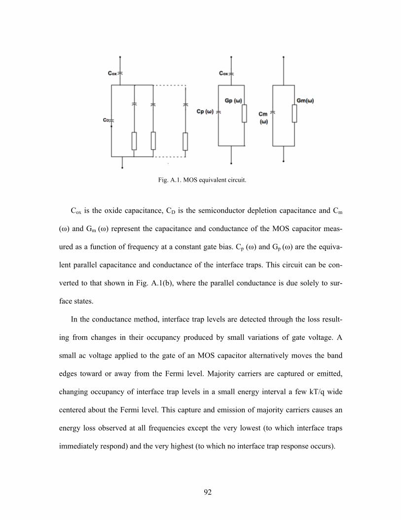
92
Cox is the oxide capacitance, CD is the semiconductor depletion capacitance and Cm
(ω) and Gm (ω) represent the capacitance and conductance of the MOS capacitor meas-
ured as a function of frequency at a constant gate bias. Cp (ω) and Gp (ω) are the equiva-
lent parallel capacitance and conductance of the interface traps. This circuit can be con-
verted to that shown in Fig. A.1(b), where the parallel conductance is due solely to sur-
face states.
In the conductance method, interface trap levels are detected through the loss result-
ing from changes in their occupancy produced by small variations of gate voltage. A
small ac voltage applied to the gate of an MOS capacitor alternatively moves the band
edges toward or away from the Fermi level. Majority carriers are captured or emitted,
changing occupancy of interface trap levels in a small energy interval a few kT/q wide
centered about the Fermi level. This capture and emission of majority carriers causes an
energy loss observed at all frequencies except the very lowest (to which interface traps
immediately respond) and the very highest (to which no interface trap response occurs).
Fig. A.1. MOS equivalent circuit.
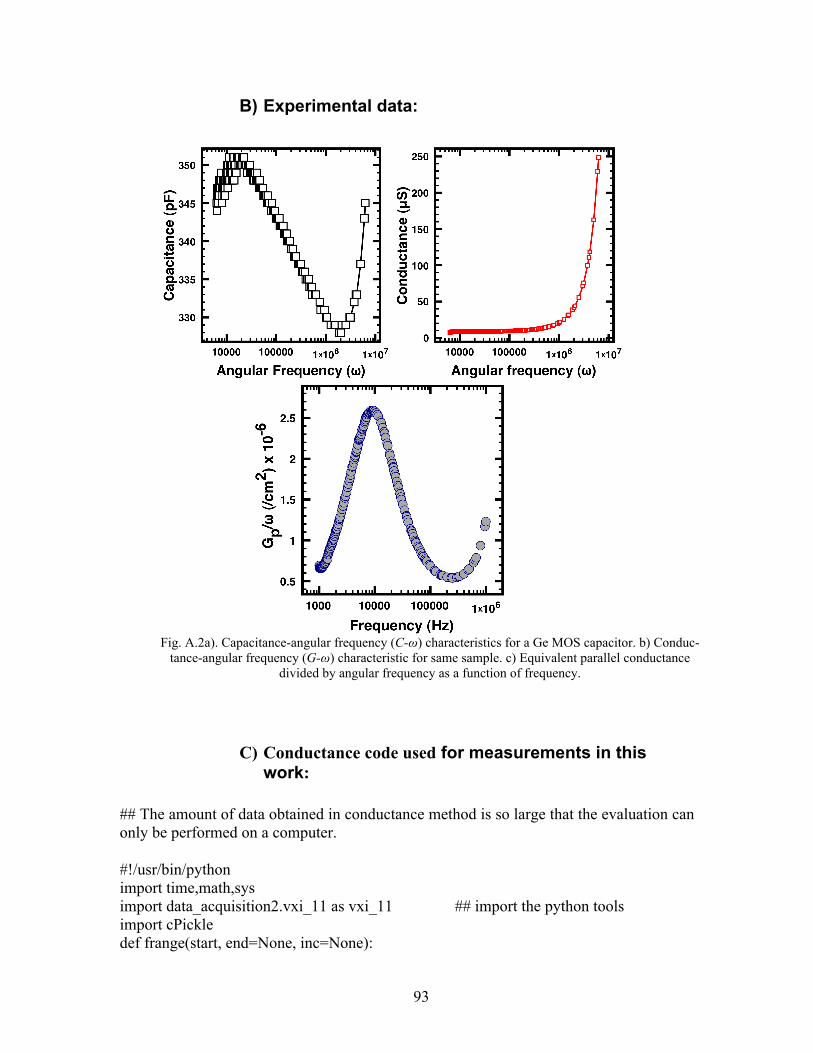
93
B) Experimental data:
C) Conductance code used for measurements in this work:
## The amount of data obtained in conductance method is so large that the evaluation can only be performed on a computer.
#!/usr/bin/python import time,math,sys import data_acquisition2.vxi_11 as vxi_11 ## import the python tools import cPickle def frange(start, end=None, inc=None):
Fig. A.2a). Capacitance-angular frequency (C-ω) characteristics for a Ge MOS capacitor. b) Conduc-
tance-angular frequency (G-ω) characteristic for same sample. c) Equivalent parallel conductance divided by angular frequency as a function of frequency.
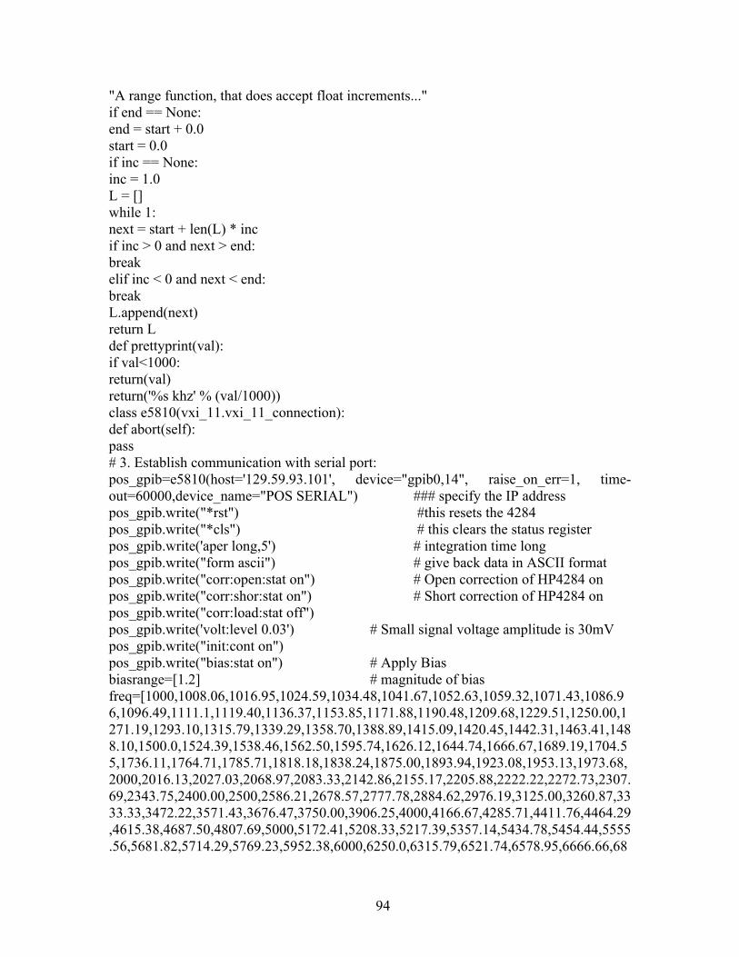
94
"A range function, that does accept float increments..." if end == None: end = start + 0.0 start = 0.0 if inc == None: inc = 1.0 L = [] while 1: next = start + len(L) * inc if inc > 0 and next > end: break elif inc < 0 and next < end: break L.append(next) return L def prettyprint(val): if val<1000: return(val) return('%s khz' % (val/1000)) class e5810(vxi_11.vxi_11_connection): def abort(self): pass # 3. Establish communication with serial port: pos_gpib=e5810(host='129.59.93.101', device="gpib0,14", raise_on_err=1, time-out=60000,device_name="POS SERIAL") ### specify the IP address pos_gpib.write("*rst") #this resets the 4284 pos_gpib.write("*cls") # this clears the status register pos_gpib.write('aper long,5') # integration time long pos_gpib.write("form ascii") # give back data in ASCII format pos_gpib.write("corr:open:stat on") # Open correction of HP4284 on pos_gpib.write("corr:shor:stat on") # Short correction of HP4284 on pos_gpib.write("corr:load:stat off") pos_gpib.write('volt:level 0.03') # Small signal voltage amplitude is 30mV pos_gpib.write("init:cont on") pos_gpib.write("bias:stat on") # Apply Bias biasrange=[1.2] # magnitude of bias freq=[1000,1008.06,1016.95,1024.59,1034.48,1041.67,1052.63,1059.32,1071.43,1086.96,1096.49,1111.1,1119.40,1136.37,1153.85,1171.88,1190.48,1209.68,1229.51,1250.00,1271.19,1293.10,1315.79,1339.29,1358.70,1388.89,1415.09,1420.45,1442.31,1463.41,1488.10,1500.0,1524.39,1538.46,1562.50,1595.74,1626.12,1644.74,1666.67,1689.19,1704.55,1736.11,1764.71,1785.71,1818.18,1838.24,1875.00,1893.94,1923.08,1953.13,1973.68,2000,2016.13,2027.03,2068.97,2083.33,2142.86,2155.17,2205.88,2222.22,2272.73,2307.69,2343.75,2400.00,2500,2586.21,2678.57,2777.78,2884.62,2976.19,3125.00,3260.87,3333.33,3472.22,3571.43,3676.47,3750.00,3906.25,4000,4166.67,4285.71,4411.76,4464.29,4615.38,4687.50,4807.69,5000,5172.41,5208.33,5217.39,5357.14,5434.78,5454.44,5555.56,5681.82,5714.29,5769.23,5952.38,6000,6250.0,6315.79,6521.74,6578.95,6666.66,68
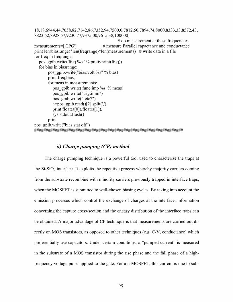
95
18.18,6944.44,7058.82,7142.86,7352.94,7500.0,7812.50,7894.74,8000,8333.33,8572.43,8823.52,8928.57,9230.77,9375.00,9615.38,100000]
# do measurement at these frequencies measurements=['CPG'] # measure Parallel capactance and conductance print len(biasrange)*len(freqrange)*len(measurements) # write data in a file for freq in freqrange: pos_gpib.write('freq %s ' % prettyprint(freq)) for bias in biasrange: pos_gpib.write("bias:volt %s" % bias) print freq,bias, for meas in measurements: pos_gpib.write('func:imp %s' % meas) pos_gpib.write("trig:imm") pos_gpib.write("fetc?") a=pos_gpib.read()[2].split(',') print float(a[0]),float(a[1]), sys.stdout.flush() print pos_gpib.write("bias:stat off") #################################################################
ii) Charge pumping (CP) method
The charge pumping technique is a powerful tool used to characterize the traps at
the Si-SiO2 interface. It exploits the repetitive process whereby majority carriers coming
from the substrate recombine with minority carriers previously trapped in interface traps,
when the MOSFET is submitted to well-chosen biasing cycles. By taking into account the
emission processes which control the exchange of charges at the interface, information
concerning the capture cross-section and the energy distribution of the interface traps can
be obtained. A major advantage of CP technique is that measurements are carried out di-
rectly on MOS transistors, as opposed to other techniques (e.g. C-V, conductance) which
preferentially use capacitors. Under certain conditions, a “pumped current” is measured
in the substrate of a MOS transistor during the rise phase and the fall phase of a high-
frequency voltage pulse applied to the gate. For a n-MOSFET, this current is due to sub-
96
strate holes which recombine, either with free electrons contained in the inversion layer
or with electrons re-emitted by interface traps.
The gate of the MOS transistor is connected to a pulse generator. Trapezoidal or tri-
angular pulses with adjustable rise and fall times are periodically applied to the gate of
the device while the source and drain are connected together and maintained at a reverse
bias (VR) with respect to the substrate. Switching the silicon surface from accumulation to
inversion, with a sufficiently large pulse amplitude, gives rise to a DC substrate current
(Fig. A.3). The current (Icp) is caused by the repetitive recombination of minority carriers
with majority carriers at the silicon-silicon oxide interface. The magnitude of this current
can be used to determine the interface-trap properties [118]. The amplitude of the DC
substrate current varies linearly with pulse frequency. For a pumped current to be meas-
ured, the amplitude of the gate pulse must exceed a threshold value.
Three charge pumping waveforms that can be used:
• Triangle Pulse: The frequency of a constant height triangle pulse is increased in
steps. At each step, substrate leakage is measured. Average interface trap density and
capture cross-section are measured by this method.
• Trapezoidal Pulse: A fixed height pulse is applied to the gate. By varying the lead-
ing/trailing edge of the pulse, you can plot interface-state density v/s energy.
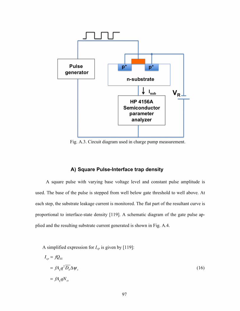
97
A) Square Pulse-Interface trap density
A square pulse with varying base voltage level and constant pulse amplitude is
used. The base of the pulse is stepped from well below gate threshold to well above. At
each step, the substrate leakage current is monitored. The flat part of the resultant curve is
proportional to interface-state density [119]. A schematic diagram of the gate pulse ap-
plied and the resulting substrate current generated is shown in Fig. A.4.
A simplified expression for Icp is given by [119]:
�
Icp = fQSS
�
= fAgq2DitΔψ s (16)
�
= fAgqNss
Fig. A.3. Circuit diagram used in charge pump measurement.
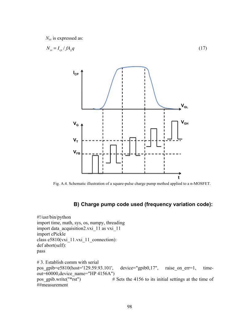
98
Nss is expressed as:
�
Nss = Icp / fAgq (17)
B) Charge pump code used (frequency variation code):
#!/usr/bin/python import time, math, sys, os, numpy, threading import data_acquisition2.vxi_11 as vxi_11 import cPickle class e5810(vxi_11.vxi_11_connection): def abort(self): pass
# 3. Establish comm with serial pos_gpib=e5810(host='129.59.93.101', device="gpib0,17", raise_on_err=1, time-out=60000,device_name="HP 4156A") pos_gpib.write("*rst") # Sets the 4156 to its initial settings at the time of ##measurement
Fig. A.4. Schematic illustration of a square-pulse charge pump method applied to a n-MOSFET.
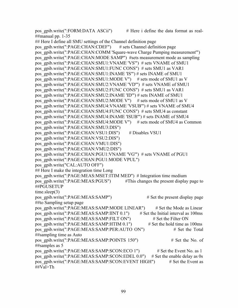
99
pos_gpib.write(":FORM:DATA ASCii") # Here i define the data format as real-##manual pp. 1-35 ## Here I define all SMU settings of the Channel definition page pos_gpib.write(":PAGE:CHAN:CDEF") # sets Channel definition page pos_gpib.write(":PAGE:CHAN:COMM 'Square-wave Charge Pumping measurement'") pos_gpib.write(":PAGE:CHAN:MODE SAMP") #sets measurement mode as sampling pos_gpib.write(":PAGE:CHAN:SMU1:VNAME 'VS'") # sets VNAME of SMU1 pos_gpib.write(":PAGE:CHAN:SMU1:FUNC CONS") # sets SMU1 as VAR1 pos_gpib.write(":PAGE:CHAN:SMU1:INAME 'IS'") # sets INAME of SMU1 pos_gpib.write(":PAGE:CHAN:SMU1:MODE V") # sets mode of SMU1 as V pos_gpib.write(":PAGE:CHAN:SMU2:VNAME 'VD'") # sets VNAME of SMU1 pos_gpib.write(":PAGE:CHAN:SMU2:FUNC CONS") # sets SMU1 as VAR1 pos_gpib.write(":PAGE:CHAN:SMU2:INAME 'ID'") # sets INAME of SMU1 pos_gpib.write(":PAGE:CHAN:SMU2:MODE V") # sets mode of SMU1 as V pos_gpib.write(":PAGE:CHAN:SMU4:VNAME 'VSUB'") # sets VNAME of SMU4 pos_gpib.write(":PAGE:CHAN:SMU4:FUNC CONS") # sets SMU4 as constant pos_gpib.write(":PAGE:CHAN:SMU4:INAME 'ISUB'") # sets INAME of SMU4 pos_gpib.write(":PAGE:CHAN:SMU4:MODE V") # sets mode of SMU4 as Common pos_gpib.write(":PAGE:CHAN:SMU3:DIS") pos_gpib.write(":PAGE:CHAN:VSU1:DIS") # Disables VSU1 pos_gpib.write(":PAGE:CHAN:VSU2:DIS") pos_gpib.write(":PAGE:CHAN:VMU1:DIS") pos_gpib.write(":PAGE:CHAN:VMU2:DIS") pos_gpib.write(":PAGE:CHAN:PGU1:VNAME 'VG'") # sets VNAME of PGU1 pos_gpib.write(":PAGE:CHAN:PGU1:MODE VPUL") pos_gpib.write("CAL:AUTO OFF") ## Here I make the integration time Long pos_gpib.write(":PAGE:MEAS:MSET:ITIM MED") # Integration time medium pos_gpib.write(":PAGE:MEAS:PGUS") #This changes the present display page to ##PGUSETUP time.sleep(3) pos_gpib.write(":PAGE:MEAS:SAMP") # Set the present display page ##to Sampling setup page pos_gpib.write(":PAGE:MEAS:SAMP:MODE LINEAR") # Set the Mode as Linear pos_gpib.write(":PAGE:MEAS:SAMP:IINT 0.1") # Set the Initial interval as 100ms pos_gpib.write(":PAGE:MEAS:SAMP:FILT ON") # Set the Filter ON pos_gpib.write(":PAGE:MEAS:SAMP:HTIM 0.1") # Set the hold time as 100ms pos_gpib.write(":PAGE:MEAS:SAMP:PER:AUTO ON") # Set the Total ##sampling time as Auto pos_gpib.write(":PAGE:MEAS:SAMP:POINTS 150") # Set the No. of ##samples as 5 pos_gpib.write(":PAGE:MEAS:SAMP:SCON:ECO 1") # Set the Event No. as 1 pos_gpib.write(":PAGE:MEAS:SAMP:SCON:EDEL 0.0") # Set the enable delay as 0s pos_gpib.write(":PAGE:MEAS:SAMP:SCON:EVENT HIGH") # Set the Event as ##Val>Th
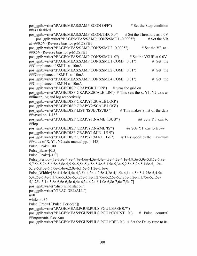
100
pos_gpib.write(":PAGE:MEAS:SAMP:SCON OFF") # Set the Stop condition ##as Disabled pos_gpib.write(":PAGE:MEAS:SAMP:SCON:THR 0.0") # Set the Threshold as 0.0V
pos_gpib.write(":PAGE:MEAS:SAMP:CONS:SMU1 -0.0005") # Set the VR at -##0.5V (Reverse bias for p-MOSFET pos_gpib.write(":PAGE:MEAS:SAMP:CONS:SMU2 -0.0005") # Set the VR at -##0.5V (Reverse bias for p-MOSFET pos_gpib.write(":PAGE:MEAS:SAMP:CONS:SMU4 0") # Set the VSUB at 0.0V pos_gpib.write(":PAGE:MEAS:SAMP:CONS:SMU1:COMP 0.01") # Set the ##Compliance of SMU1 as 10mA pos_gpib.write(":PAGE:MEAS:SAMP:CONS:SMU2:COMP 0.01") # Set the ###Compliance of SMU1 as 10mA pos_gpib.write(":PAGE:MEAS:SAMP:CONS:SMU4:COMP 0.01") # Set the ##Compliance of SMU4 as 10mA pos_gpib.write(":PAGE:DISP:GRAP:GRID ON") # turns the grid on pos_gpib.write(":PAGE:DISP:GRAP:X:SCALE LIN") # This sets the x, Y1, Y2 axis as ##linear, log and log respectively pos_gpib.write(":PAGE:DISP:GRAP:Y1:SCALE LOG") pos_gpib.write(":PAGE:DISP:GRAP:Y2:SCALE LOG") pos_gpib.write(":PAGE:DISP:LIST 'ISUB','IS','ID'") # This makes a list of the data ##saved pp. 1-153 pos_gpib.write(":PAGE:DISP:GRAP:Y1:NAME 'ISUB'") ## Sets Y1 axis to ##Icp pos_gpib.write(":PAGE:DISP:GRAP:Y2:NAME 'IS'") ## Sets Y1 axis to Icp## pos_gpib.write(":PAGE:DISP:GRAP:Y1:MIN -1E-9") pos_gpib.write(":PAGE:DISP:GRAP:Y1:MAX 1E-9") # This specifies the maximum ##value of X, Y1, Y2 axis-manual pp. 1-148 Pulse_Peak=1.00 Pulse_Base=[0.5] Pulse_Peak=[-1.0] Pulse_Period=[1e-3,9e-4,8e-4,7e-4,6e-4,5e-4,4e-4,3e-4,2e-4,1e-4,9.5e-5,9e-5,8.5e-5,8e-5,7.5e-5,7e-5,6.5e-5,6e-5,5.5e-5,5e-5,4.5e-5,4e-5,3.5e-5,3e-5,2.5e-5,2e-5,1.6e-5,1.2e-5,1e-5,8.0e-6,6.0e-6,4e-6,2.0e-6,1.6e-6,1.2e-6,1e-6] Pulse_Width=[5e-4,4.5e-4,4e-4,3.5e-4,3e-4,2.5e-4,2e-4,1.5e-4,1e-4,5e-5,4.75e-5,4.5e-5,4.25e-5,4e-5,3.75e-5,3.5e-5,3.25e-5,3e-5,2.75e-5,2.5e-5,2.25e-5,2e-5,1.75e-5,1.5e-5,1.25e-5,1e-5,8e-6,6e-6,5e-6,4e-6,3e-6,2e-6,1.0e-6,8e-7,6e-7,5e-7] pos_gpib.write(":disp:wind:stat on") pos_gpib.write(":TRAC:DEL:ALL") n=0 while n< 36: Pulse_Freq=1/(Pulse_Period[n]) pos_gpib.write(":PAGE:MEAS:PGUS:PULS:PGU1:BASE 0.7") pos_gpib.write(":PAGE:MEAS:PGUS:PULS:PGU1:COUNT 0") # Pulse count=0 ##represents Free Run pos_gpib.write(":PAGE:MEAS:PGUS:PULS:PGU1:DEL 0") # Set the Delay time to 0s
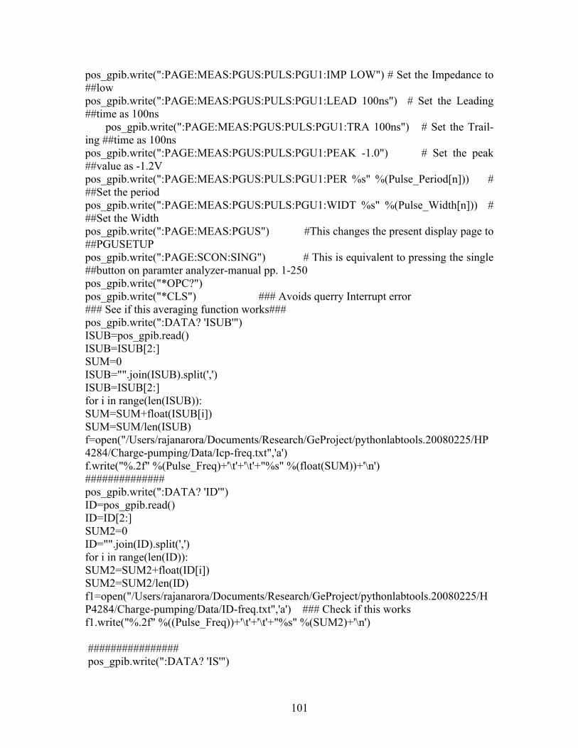
101
pos_gpib.write(":PAGE:MEAS:PGUS:PULS:PGU1:IMP LOW") # Set the Impedance to ##low pos_gpib.write(":PAGE:MEAS:PGUS:PULS:PGU1:LEAD 100ns") # Set the Leading ##time as 100ns
pos_gpib.write(":PAGE:MEAS:PGUS:PULS:PGU1:TRA 100ns") # Set the Trail-ing ##time as 100ns pos_gpib.write(":PAGE:MEAS:PGUS:PULS:PGU1:PEAK -1.0") # Set the peak ##value as -1.2V pos_gpib.write(":PAGE:MEAS:PGUS:PULS:PGU1:PER %s" %(Pulse_Period[n])) # ##Set the period pos_gpib.write(":PAGE:MEAS:PGUS:PULS:PGU1:WIDT %s" %(Pulse_Width[n])) # ##Set the Width pos_gpib.write(":PAGE:MEAS:PGUS") #This changes the present display page to ##PGUSETUP pos_gpib.write(":PAGE:SCON:SING") # This is equivalent to pressing the single ##button on paramter analyzer-manual pp. 1-250 pos_gpib.write("*OPC?") pos_gpib.write("*CLS") ### Avoids querry Interrupt error ### See if this averaging function works### pos_gpib.write(":DATA? 'ISUB'") ISUB=pos_gpib.read() ISUB=ISUB[2:] SUM=0 ISUB="".join(ISUB).split(',') ISUB=ISUB[2:] for i in range(len(ISUB)): SUM=SUM+float(ISUB[i]) SUM=SUM/len(ISUB) f=open("/Users/rajanarora/Documents/Research/GeProject/pythonlabtools.20080225/HP4284/Charge-pumping/Data/Icp-freq.txt",'a') f.write("%.2f" %(Pulse_Freq)+'\t'+'\t'+"%s" %(float(SUM))+'\n') ############## pos_gpib.write(":DATA? 'ID'") ID=pos_gpib.read() ID=ID[2:] SUM2=0 ID="".join(ID).split(',') for i in range(len(ID)): SUM2=SUM2+float(ID[i]) SUM2=SUM2/len(ID) f1=open("/Users/rajanarora/Documents/Research/GeProject/pythonlabtools.20080225/HP4284/Charge-pumping/Data/ID-freq.txt",'a') ### Check if this works f1.write("%.2f" %((Pulse_Freq))+'\t'+'\t'+"%s" %(SUM2)+'\n') ################ pos_gpib.write(":DATA? 'IS'")
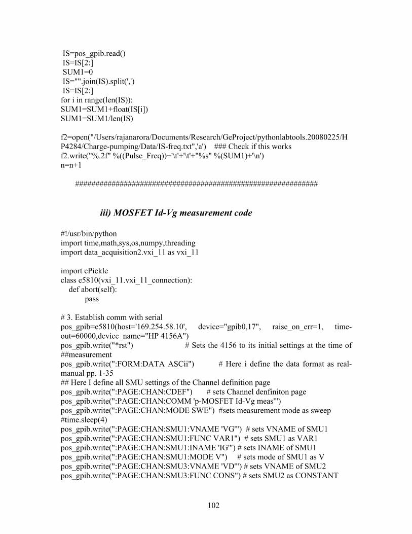
102
IS=pos_gpib.read() IS=IS[2:] SUM1=0 IS="".join(IS).split(',') IS=IS[2:] for i in range(len(IS)): SUM1=SUM1+float(IS[i]) SUM1=SUM1/len(IS) f2=open("/Users/rajanarora/Documents/Research/GeProject/pythonlabtools.20080225/HP4284/Charge-pumping/Data/IS-freq.txt",'a') ### Check if this works f2.write("%.2f" %((Pulse_Freq))+'\t'+'\t'+"%s" %(SUM1)+'\n') n=n+1
############################################################
iii) MOSFET Id-Vg measurement code
#!/usr/bin/python import time,math,sys,os,numpy,threading import data_acquisition2.vxi_11 as vxi_11 import cPickle class e5810(vxi_11.vxi_11_connection): def abort(self): pass # 3. Establish comm with serial pos_gpib=e5810(host='169.254.58.10', device="gpib0,17", raise_on_err=1, time-out=60000,device_name="HP 4156A") pos_gpib.write("*rst") # Sets the 4156 to its initial settings at the time of ##measurement pos_gpib.write(":FORM:DATA ASCii") # Here i define the data format as real-manual pp. 1-35 ## Here I define all SMU settings of the Channel definition page pos_gpib.write(":PAGE:CHAN:CDEF") # sets Channel denfiniton page pos_gpib.write(":PAGE:CHAN:COMM 'p-MOSFET Id-Vg meas'") pos_gpib.write(":PAGE:CHAN:MODE SWE") #sets measurement mode as sweep #time.sleep(4) pos_gpib.write(":PAGE:CHAN:SMU1:VNAME 'VG'") # sets VNAME of SMU1 pos_gpib.write(":PAGE:CHAN:SMU1:FUNC VAR1") # sets SMU1 as VAR1 pos_gpib.write(":PAGE:CHAN:SMU1:INAME 'IG'") # sets INAME of SMU1 pos_gpib.write(":PAGE:CHAN:SMU1:MODE V") # sets mode of SMU1 as V pos_gpib.write(":PAGE:CHAN:SMU3:VNAME 'VD'") # sets VNAME of SMU2 pos_gpib.write(":PAGE:CHAN:SMU3:FUNC CONS") # sets SMU2 as CONSTANT
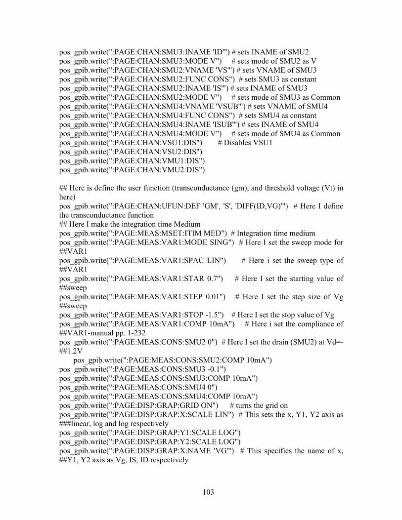
103
pos_gpib.write(":PAGE:CHAN:SMU3:INAME 'ID'") # sets INAME of SMU2 pos_gpib.write(":PAGE:CHAN:SMU3:MODE V") # sets mode of SMU2 as V pos_gpib.write(":PAGE:CHAN:SMU2:VNAME 'VS'") # sets VNAME of SMU3 pos_gpib.write(":PAGE:CHAN:SMU2:FUNC CONS") # sets SMU3 as constant pos_gpib.write(":PAGE:CHAN:SMU2:INAME 'IS'") # sets INAME of SMU3 pos_gpib.write(":PAGE:CHAN:SMU2:MODE V") # sets mode of SMU3 as Common pos_gpib.write(":PAGE:CHAN:SMU4:VNAME 'VSUB'") # sets VNAME of SMU4 pos_gpib.write(":PAGE:CHAN:SMU4:FUNC CONS") # sets SMU4 as constant pos_gpib.write(":PAGE:CHAN:SMU4:INAME 'ISUB'") # sets INAME of SMU4 pos_gpib.write(":PAGE:CHAN:SMU4:MODE V") # sets mode of SMU4 as Common pos_gpib.write(":PAGE:CHAN:VSU1:DIS") # Disables VSU1 pos_gpib.write(":PAGE:CHAN:VSU2:DIS") pos_gpib.write(":PAGE:CHAN:VMU1:DIS") pos_gpib.write(":PAGE:CHAN:VMU2:DIS") ## Here is define the user function (transconductance (gm), and threshold voltage (Vt) in here) pos_gpib.write(":PAGE:CHAN:UFUN:DEF 'GM', 'S', 'DIFF(ID,VG)'") # Here I define the transconductance function ## Here I make the integration time Medium pos_gpib.write(":PAGE:MEAS:MSET:ITIM MED") # Integration time medium pos_gpib.write(":PAGE:MEAS:VAR1:MODE SING") # Here I set the sweep mode for ##VAR1 pos_gpib.write(":PAGE:MEAS:VAR1:SPAC LIN") # Here i set the sweep type of ##VAR1 pos_gpib.write(":PAGE:MEAS:VAR1:STAR 0.7") # Here I set the starting value of ##sweep pos_gpib.write(":PAGE:MEAS:VAR1:STEP 0.01") # Here I set the step size of Vg ##sweep pos_gpib.write(":PAGE:MEAS:VAR1:STOP -1.5") # Here I set the stop value of Vg pos_gpib.write(":PAGE:MEAS:VAR1:COMP 10mA") # Here i set the compliance of ##VAR1-manual pp. 1-232 pos_gpib.write(":PAGE:MEAS:CONS:SMU2 0") # Here I set the drain (SMU2) at Vd=-##1.2V
pos_gpib.write(":PAGE:MEAS:CONS:SMU2:COMP 10mA") pos_gpib.write(":PAGE:MEAS:CONS:SMU3 -0.1") pos_gpib.write(":PAGE:MEAS:CONS:SMU3:COMP 10mA") pos_gpib.write(":PAGE:MEAS:CONS:SMU4 0") pos_gpib.write(":PAGE:MEAS:CONS:SMU4:COMP 10mA") pos_gpib.write(":PAGE:DISP:GRAP:GRID ON") # turns the grid on pos_gpib.write(":PAGE:DISP:GRAP:X:SCALE LIN") # This sets the x, Y1, Y2 axis as ###linear, log and log respectively pos_gpib.write(":PAGE:DISP:GRAP:Y1:SCALE LOG") pos_gpib.write(":PAGE:DISP:GRAP:Y2:SCALE LOG") pos_gpib.write(":PAGE:DISP:GRAP:X:NAME 'VG'") # This specifies the name of x, ##Y1, Y2 axis as Vg, IS, ID respectively
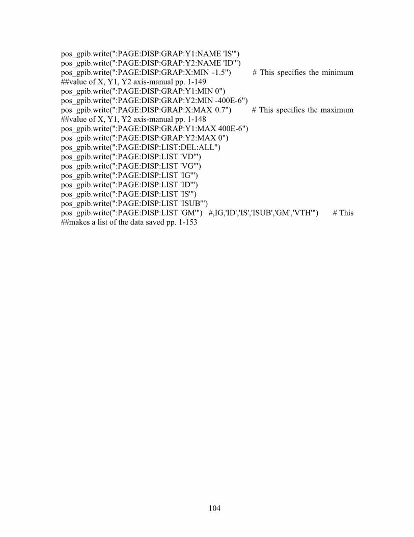
104
pos_gpib.write(":PAGE:DISP:GRAP:Y1:NAME 'IS'") pos_gpib.write(":PAGE:DISP:GRAP:Y2:NAME 'ID'") pos_gpib.write(":PAGE:DISP:GRAP:X:MIN -1.5") # This specifies the minimum ##value of X, Y1, Y2 axis-manual pp. 1-149 pos_gpib.write(":PAGE:DISP:GRAP:Y1:MIN 0") pos_gpib.write(":PAGE:DISP:GRAP:Y2:MIN -400E-6") pos_gpib.write(":PAGE:DISP:GRAP:X:MAX 0.7") # This specifies the maximum ##value of X, Y1, Y2 axis-manual pp. 1-148 pos_gpib.write(":PAGE:DISP:GRAP:Y1:MAX 400E-6") pos_gpib.write(":PAGE:DISP:GRAP:Y2:MAX 0") pos_gpib.write(":PAGE:DISP:LIST:DEL:ALL") pos_gpib.write(":PAGE:DISP:LIST 'VD'") pos_gpib.write(":PAGE:DISP:LIST 'VG'") pos_gpib.write(":PAGE:DISP:LIST 'IG'") pos_gpib.write(":PAGE:DISP:LIST 'ID'") pos_gpib.write(":PAGE:DISP:LIST 'IS'") pos_gpib.write(":PAGE:DISP:LIST 'ISUB'") pos_gpib.write(":PAGE:DISP:LIST 'GM'") #,IG,'ID','IS','ISUB','GM','VTH'") # This ##makes a list of the data saved pp. 1-153
105
REFERENCES
[1] G. E. Moore, “Cramming more components onto integrated circuits”, Electronics, Vol .38, 1965.
[2] G. D. Wilk, R. M. Wallace, and J. M. Anthony, “Hafnium and zirconium silicates for advanced gate dielectrics”, Journal of Applied Physics, vol. 87, pp. 484-492, 2000.
[3] http://www.itrs.net/
[4] R. W. Dutton and A. J. Strojwas, “Perspectives on technology and technology-driven CAD”, IEEE
Transactions on Computer-aided Design of Integrated Circuits and Systems, Vol .19, pp. 1544-1560, 2000.
[5] http://www.intel.com/technology/silicon/high-κ.html.
[6] D. A. Buchanan, E. P. Gusev, E. Cartier, H. O. Schmidt, K. Rim, M. A. Gribelyuk, A. Mocuta, A.
Ajmera, M. Copel, S. Guha, N. Bojarczuk, A. Callegari, C. D. Emic, P. Kozlowski, K. Chan, R. J. Fleming, P. C. Jamison, J. Brown and R. Arndt, “ 80 nm poly-silicon gates n-FETs with ultra-thin Al2O3 gate dielectric for ULSI applications”, IEEE International Electron Devices Meeting, pp. 223-226, 2000.
[7] Y. C. Yeo, Q. Lu, T. King, C. Hu, T. Kawashima, M. Oishi, S. Mashiro, and J. Sakai, “Enhanced
performance in sub-100nm CMOSFETs using strained epitaxial silicon-germanium,” IEEE Inter-national Electron Devices Meeting, pp.753, 2000.
[8] K. Rim, S. Koester, M. Hargrove, J. Chu, P. M. Mooney, J. Ott, T. Kanarsky, P. Ronsheim, M.
Ieong, A. Grill, and H. S. P. Wong, “Strained Si NMOSFETs for high performance CMOS tech-nology”, IEEE Symposium on VLSI Technology, pp. 59, 2001.
[9] S. M. Sze, Physics of Semiconductor Devices, 2nd edition, pp. 46, 1981.
[10] C. O. Chui, S. Ramanathan, B. B. Triplett, P. C. McIntyre, and K. C. Saraswat, “Germanium MOS
capacitors incorporating ultrathin high-κ gate dielectric”, IEEE Electron Device Letters, Vol. 23, pp. 473-475, 2002.
[11] Cor Claeys and Eddy Simoen (eds.), Germanium-based technologies: From materials to devices,
Elsevier Science, 2007.
[12] G. E. Stillman, V. M. Robbins and N. Tabatabaie, “III-V compound semiconductor devices: Opti-cal detectors”, IEEE Transactions on Electron Devices, Vol. 31, pp. 1643-1655, 1984.
[13] J. Mitard, B. D. Jaeger, F. E. Leys, G. Hellings, K. Martens, G. Eneman, D. P. Brunco, R. Loo, J. C.
Lin, D. Shamiryan, T. Vandeweyer, G. Winderickx, E. Vrancken, C. H. Yu, K. D. Meyer, M. Caymax, L. Pantisano, M. Meuris and M. M. Heyns, “Record Ion/Ioff performance of 65 nm Ge p-MOSFET and novel Si passivation scheme for improved EOT scalability”, IEEE International Electron Devices Meeting (IEDM), 2008.
[14] J. Mitard, C. Shea, B. D Jaeger, A. Pristera, G. Wang, M. Houssa, G. Eneman, G. Hellings, W.
Wang, J. Lin, F. Leys, R. Loo, G. Winderickx, E. Vrancken, A. Stesmans, K. D. Meyer, M. Cay-max, L. Pantisano, M. Meuris and M. Heyns, "Impact of EOT scaling down to 0.85 nm on 70 nm Ge-pFETs technology with STI", to be published at VLSI Symposium, Kyoto, Japan, Jun. 2009.
[15] K. Martens, C. O. Chui, G. Brammertz, B. D. Jaeger, D. Kuzum, M. Meuris, M. M. Heyns, T.
Krishnamohan, K. Saraswat, H. E. Maes, and G. Groeseneken, “On the correct extraction of inter-
106
face trap density of MOS devices with high-mobility semiconductor substrates”, IEEE Transac-tions on Electron Devices, Vol. 55, pp. 547-556, 2008.
[16] Y. Xuan, Y. Q. Wu and P. D. Ye, “High-performance inversion-type enhancement-mode InGaAs
MOSFET with maximum drain current exceeding 1A/mm”, IEEE Electron Device Letters, Vol. 29, pp. 294-296, 2008.
[17] H. Becke, R. Hall, and J. White, “Gallium arsenide MOS transistors”, Solid State Electronics, vol.
8, pp. 813-823, 1965.
[18] S. Datta, “III-V field-effect transistors for low power digital logic application”, Microelectronic Engineering, Vol. 84, 2133-2137, 2007.
[19] M. Bhatnagar and B. J. Baliga, “Comparison of 6H-SiC, 3C-SiC, and Si for power devices”, IEEE
Transactions on Electron Devices, Vol. 40, pp. 645-655, 1993.
[20] G. Y. Chung, C. C. Tin, J. R. Williams, K. McDonald, R. K. Chanana, R. A. Weller, S. T. Pantelides, L. C. Feldman, O. W. Holland, M. K. Das, J. W. Palmour, “Improved inversion channel mobility for 4H-SiC MOSFETs following high temperature anneals in nitric oxide”, IEEE Electron Device Letters, Vol. 22, pp. 176-178, 2001.
[21] H. F. Li, S. Dimitrijev, H. B. Harrison, and D. Sweatman, “Interfacial characteristics of N2O and
NO nitrided SiO2 grown on SiC by rapid thermal processing”, Applied Physics Letters, Vol. 70, pp. 2028-2030, 1997.
[22] K. Jarrendahl and R. F. Davis, SiC materials and devices, pp. 1-20, Academic Press London,
1998.
[23] P. Jamet, S. Dimitrijev, P. Tanner, “ Effects of nitridation on gate oxides grown on 4H-SiC”, Journal of Applied Physics, Vol. 90, pp. 5058-5063, 2001.
[24] S. Dimitrijev, H. F. Li, H. B. Harrison, D. Sweatman, “Nitridation of silicon-dioxide films grown
on 6H silicon carbide”, IEEE Electron Device Letters, Vol. 18, pp. 175-177, 1997.
[25] P. T. Lai, J. P. Xu, Y. C. Cheng, “Interface properties of NO-annealed N2O-grown oxynitride”, IEEE Transactions on Electron Devices, Vol. 46, pp. 2311-2314, 1999.
[26] S. Chakraborty, P. T. Lai, P. C. K. Kwok, “MOS characteristics of NO-grown oxynitrides on n-
type 6H-SiC”, Microelectronics Reliability, Vol. 42, pp. 455-457, 2002.
[27] P. Jamet, S. Dimitrijev, “Physical properties of N2O and NO-nitrided gate oxides grown on 4H SiC”, Applied Physics Letters, Vol. 79, pp. 323-325, 2001.
[28] P. Tanner, S. Dimtrijev, H. F. li, D. Sweatman, K. E. Prince, H. B. Harrison, “SIMS analysis of ni-
trided oxides grown on 4H-SiC”, Journal of Electronic Materials, Vol. 28, pp. 109-111, 1999.
[29] V. V. Afanas’eV, M. Bassler, G. Pensl, and M. J. Schulz, “Intrinsic SiC/SiO2 interface traps”, Physica Status Solidi A, Vol. 162, pp. 321-337, 1997.
[30] K. Fukuda, W. J. Cho, K. Arai, S. Suzuki, J. Senzaki, and T. Tanak, “Effect of oxidation method
and post-oxidation annealing on interface properties of metal–oxide–semiconductor structures formed on n-type 4H-SiC C(
�
0001) face”, Applied Physics Letters, Vol . 77, pp. 866-868, 2000.
[31] F. Lanois, D. Planson, P. Lassagne, C. Raymond, and E. Bano, “6H-SiC MOS capacitors on sloped surfaces - Realisation, characterisation and electrical results”, Materials Science Forum, Vol. 264, pp. 1029-1032, 1998.
107
[32] E. G. Stein von Kamienski, F. Portheine, J. Stein, A. Golz, and H. kurz, “Charge trapping in dry and wet oxides on N-type 6H–SiC studied by Fowler–Nordheim charge injection”, Journal of Ap-plied Physics, Vol. 79, 2529, 1996.
[33] J. Campi, Y. Shi, Y. Luo, F. Yan, and J. H. Zhao, “Study of interface trap density and effective oxide charge in post-metallization annealed SiO2-SiC structures”, IEEE Transactions on Electron Devices, Vol. 46, pp. 511-519, 1999.
[34] P. Friedrichs, E. P. Burte, and R. Schorner, “Interface properties of metal-oxide-semiconductor
structures on n-type 6H and 4H-SiC”, Journal of Applied Physics, Vol. 79, 7814, 1996.
[35] V. V. Afanas’ev, A. Stesmans, F. Ciobanu, G. Pensl, K. Y. Cheong, and S. Dimitrijev, “Mecha-nisms responsible for improvement of 4H–SiC/SiO2 interface properties by nitridation”, Applied Physics Letters, Vol . 82, 568, 2003.
[36] P. Paillet, J. R. Schwank, M. R. Shaneyfelt, V. Ferlet-Cavrois, R. L. Jones, O. Flament, and E. W.
Blackmore, “Total dose hardness assurance testing using laboratory radiation sources”, IEEE Transactions on Nuclear Science, Vol. 50, pp. 2310-2315, 2003.
[37] J. R. Schwank, M. R. Shaneyfelt, P. Paillet, D. E. Beutler, V. Ferlet-Cavrois, B. L. Draper, R. A.
Loemker, P. E. Dodd, and F. W. Sexton, “Optimum laboratory radiation source for hardness as-surance testing”, IEEE Transactions on Nuclear Science, Vol. 48, pp. 2152-2157, 2001.
[38] M. R. Shaneyfelt, K. L. Hughes, J. R. Schwank, F. W. Sexton, D. M. Fleetwood, P. S. Winokur,
and E. W. Enlow, “Wafer-level radiation testing for hardness assurance”, IEEE Transactions on Nucear Science, Vol. 38, pp. 1598–1605, Dec. 1991.
[39] B. E. Deal, “Standardized terminology for oxide charges associated with thermally oxidized sili-
con”, IEEE Transactions on Electron Devices, Vol. ED-27, no. 3, pp. 606-607, 1980.
[40] P. M. Lenahan and P. V. Dressendorfer, “Hole traps and trivalent silicon centers in MOS devices”, Journal of Applied Physics, Vol. 55, pp. 3495-3499, 1984.
[41] D. M. Fleetwood, “Border traps in MOS devices”, IEEE Transactions on Nuclear Science, Vol.
39, pp. 269-271, 1992.
[42] D. M. Fleetwood and N. S. Saks, “Oxide, interface, and border traps in thermal, N2O, and N2O-nitrided oxides”, Journal of Applied Physics, Vol. 79, pp. 1583-1594, 1996.
[43] Y. Murakami and T. Shingyouji, “Separation and analysis of diffusion and generation components
of pn junction leakage current in various silicon wafers”, Journal of Applied Physics, Vol. 75, pp. 3548-3552, 1994.
[44] D. Zupac, K. F. Galloway, P. Khosropour, S. R. Anderson, and R. D. Schrimpf, “Separation of ef-
fects of oxide-trapped charge and interface-trapped charge on mobility in irradiated power MOS-FETs”, IEEE Transactions on Nuclear Science, Vol. 40, pp. 1307-1315, 1993.
[45] J. A. Felix, D. M. Fleetwood, R. D. Schrimpf, J. G. Hong, G. Lucovsky, J. R. Schwank, and M. R.
Shaneyfelt, “Total-dose radiation response of hafnium-silicate capacitors,” IEEE Transactions on Nuclear Science, Vol. 49, no. 6, pp. 3191-3196, 2002.
[46] J. A. Felix, M. R. Shaneyfelt, D. M. Fleetwood, T. L. Meisenheimer, J. R. Schwank, R. D.
Schrimpf, P. E. Dodd, E. P. Gusev, and C. D’ Emic, “Radiation-induced charge trapping in thin Al2O3/SiOxNy/Si(100) gate dielectric stacks,” IEEE Transactions on Nuclear Science, Vol. 50, no. 6, pp. 1910-1918, 2003.
108
[47] J. A. Felix, H. D. Xiong, D. M. Fleetwood, E. P. Gusev, R. D. Schrimpf, A. L. Sternberg, and C. D’Emic, “Interface trapping properties of nMOSFETs with Al2O3/SiOxNy/Si(100) gate dielectric stacks after exposure to ionizing radiation,” Microelectronic Engineering, Vol. 72, no. 1-4, pp. 50-54, 2004.
[48] X. J. Zhou, D. M. Fleetwood, J. A. Felix, E. P. Gusev, and C. D’Emic, “Bias-temperature insta-
bilities and radiation effects in MOS devices,” IEEE Transactions on Nuclear Science, Vol. 52, no. 6, pp. 2231-2238, 2005.
[49] S. K. Dixit, X. J. Zhou, R. D. Schrimpf, D. M. Fleetwood, S. T. Pantelides, R. Choi, G. Bersuker,
and L. C. Feldman, "Radiation induced charge trapping in ultrathin HfO2-based MOSFETs," IEEE Transactions on Nuclear Science, Vol. 54, p. 1883, 2007.
[50] D. K. Chen, F. E. Mamouni, X. J. Zhou, R. D. Schrimpf, D. M. Fleetwood, K. F. Galloway, S.
Lee, H. Seo, G. Lucovsky, B. Jun, and J. D. Cressler, “Total dose and bias temperature stress ef-fects for HfSiON on Si MOS capacitors”, IEEE Transactions on Nuclear Science, Vol. 54, p. 1931-1937, 2007.
[51] Y. Miura and Y. Matukura, “ Investigation of silicon–silicon dioxide interface using MOS struc-
ture”, Japanese Journal of Applied Physics, Vol. 5, pp.180, 1966. A. Goetzberger, H. E. Nigh, “Surface charge after annealing of Al–SiO2– Si structures under
bias”, Proceedings of IEEE, Vol. 54, pp.1454, 1966.
[52] C. Shen, M. –F. Li, C. E. Foo, T. Yang, D. M. Huang, A. Yap, G. S. Samudra, Y. –C. Yeo, “Char-acterization and physical origin of fast Vth transient in NBTI of p-MOSFETs with SiON dielec-tric”, IEEE International Electron Device Meeting (IEDM), pp. 1-4, 2006.
[53] V. Huard, F. Monsieur, G. Ribes, S. Bruyere, “Evidence for hydrogen-related defects during NBTI stress in p-MOSFETs”, IEEE International Reliability Physics Symposium, pp. 178-182, 2003.
[54] M. A. Alam, S. Mahapatra, “A comprehensive model of PMOS NBTI degradation”, Microelec-
tronics Reliability, Vol. 45, pp. 71–81, 2005.
[55] K. O. Jeppson, C. M. Svensson, “Negative bias stress of MOS devices at high electric fields and degradation of MNOS devices”, Journal of Applied Physics, Vol. 48, pp. 2004–2014, 1977.
[56] S. Ogawa, N. Shiono, “Generalized diffusion–reaction model for the low-field charge build up in-
stability at the Si–SiO2 interface”, Physical Review, Vol. 51, pp. 4218–4230, 1995.
[57] D. K. Schroeder, “Negative bias temperature instability: What do we understand?”, Microelec-tronics Engineering, Vol. 47, pp. 841-852, 2007.
[58] E. H. Poindexter, P. J. Caplan, “Characterization of Si/SiO2 interface defects by electron spin
resonance”, Progress in Surface Science, Vol. 14, 201–294, 1983.
[59] M. L. Reed, J. D. Plummer, “Chemistry of Si–SiO2 interface trap annealing”, Journal of Applied Physics, Vol. 63, pp. 5776–5793, 1988.
[60] A. Stirling, A. Pasquarello, J. C. Charlier, R. Car, “Dangling bond defects at SiO2/Si interfaces:
atomic structure of the Pb1 center”, Physical Review Letter, Vol. 85, 2773–2776, 2000.
[61] A. Stesmans, V. V. Afanase´v, “Nature of the Pb1 defect in (100)Si/SiO2 as revealed by electron spin resonance 29Si hyperfine structure”, Microelectronics Engineering, Vol. 48, 113–116, 1999.
[62] A. Stesmans, V. V. Afanase´v, “Electrical activity of interfacial paramagnetic defects in thermal
(100)Si/SiO2”, Physical Review, Vol. 57, 10030–4, 1998.
109
[63] P. Lenahan, IEEE Reliability Physics Tutorial Notes, Advanced Related Topics (IRPS), 2002.
[64] J. C. Campbell, P. M. Lenahan, “Density of states of Pb1 Si/SiO2 interface trap centers”, Applied Physics Letters, Vol. 80, 1945–7, 2002.
[65] D. M. Fleetwood, “Long-term annealing study of midgap interface-trap charge neutrality”, Ap-
plied Physics Letters, Vol. 60, 2883–5, 1992.
[66] K. Saminadayar, J. C. Pfister, “Evolution of surface-states density of Si/wet thermal SiO2 interface during bias-temperature treatment”, Solid-State Electronics, Vol. 20, 891–6, 1977.
[67] R. Jayaraman, C. G. Sodini, “A 1/f noise technique to extract the oxide trap density near the con-
duction band edge of silicon”, IEEE Transactions on Electron Devices, Vol. 36, 1773–82, 1989.
[68] Y. Mitani, M. Nagamine, H. Satake, A. Toriumi, “NBTI mechanism in ultra-thin gate dielectric-nitrogen-originated mechanism in SiON”, IEEE International Electron Devices Meeting (IEDM), 509–12, 2002.
[69] T. P. Ma and P. V. Dressendorfer, Eds., Ionizing radiation effects in MOS devices and circuits.
New York: Wiley Interscience, 1989.
[70] T. R. Oldham and F. B. McLean, “Total ionizing dose effects in MOS oxides and devices,” IEEE Transactions on Nuclear Science, Vol. 50, no. 3, pp. 483-499, Jun. 2003.
[71] S. K. Dixit, X. J. Zhou, R. D. Schrimpf, D. M. Fleetwood, S. T. Pantelides, R. Choi, G. Bersuker,
and L. C. Feldman, “Radiation induced charge trapping in ultrathin HfO2 based MOSFETs,” IEEE Transactions on Nuclear Science, Vol. 54, no. 6, pp.1883-1890, Dec. 2007.
[72] D. K. Chen, R. D. Schrimpf, D. M. Fleetwood, K. F. Galloway, S. T. Pantelides, A. Dimoulas, G.
Mavrou, A. Sotiropoulos and Y. Panayiotatos “Total dose response of Ge MOS capacitors with HfO2/Dy2O3 gate stacks,” IEEE Transactions on Nuclear Science, Vol. 54, no. 4, pp. 971-974, Aug. 2007.
[73] J. A. Croon, B. Kaczer. G. S. Lujan, S. Kubicek, G. Groeseneken, and M. Meuris, “Experimental
analysis of Ge-HfO2-TaN gate stack with a large amount of interface traps,” Proceedings of 2005 IEEE International Conference on Microelectronic Test Structures, pp. 191-196, April 2005.
[74] S. Zhu, R. Li, S. J. Lee, M. F. Li, A. Du, J. Singh, C. Zhu, A. Chin, and D. L. Kwong, “Germa-
nium pMOSFETs with Schottky-barrier germanide S/D, high-κ gate dielectric and metal gate,” IEEE Electron Device Letters, Vol. 26, no. 2, pp. 81-83, Feb. 2005.
[75] S. C. Martin, L. M. Hitt, and J. J. Rosenberg, “p-channel germanium MOSFET’s with high chan-
nel mobility,” IEEE Electron Device Letters, Vol. 10, no. 7, pp. 325-326, Jul. 1989.
[76] C. O. Chui, H. Kim, D. Chi, B. B. Triplett, P. C. McIntyre, and K. C. Saraswat, “ A sub-400 °C germanium MOSFET technology with high-κ dielectric and metal gate,” IEDM Technlogy Digest, pp. 437- 440, 2002.
[77] C. Le Royer. B. Vincent, L. Clavelier, J. -F. Damlencourt, C. Tabone, P. Batude, D. Blachier, R.
Truche, Y. Campidelli, Q.T. Nguyen, S. Cristoloveanu, S. Soliveres, G. Le Carval, F. Boulanger, T. Billon, D. Bensahel, and S. Deleonibus, “High-k and metal gate pMOSFETs on GeOI obtained by Ge enrichment: Analysis of on and off performance,” IEEE Electron Device Letters, Vol. 29, pp. 635-637, no. 6, Jun. 2008.
[78] I. S. Esqueda, H. J. Barnaby and M. L. Alles, “Two dimensional methodology for modeling radia-
tion induced off-state leakage in CMOS technology,” IEEE Transactions on Nuclear Science, Vol.
110
52, no. 6, pp. 2259-2264, Dec. 2005.
[79] M. A. Krylov and S. V. Malyanov, “Effects of x-rays on the electrophysical properties of germa-nium and germanium p-n junctions,” Russian Physics Journal, Vol. 9, no. 4, pp. 103-109, Jul. 1966.
[80] C. E. Lindberg, J. Lundsgaard, P. Bomholt, A. Mesil, K. Bonde Nielsen, A. Nylandsted Larsen,
and L. Dobaczewski, “The antimony-vacancy defect in p-type germanium,” Applied Physics Let-ters, vol. 87, article no. 172103, 2005.
[81] E. Simoen, C. Claeys, J. Vanhellemont, “Defect analysis in semiconductor materials based on p-n
Junction Diode Characteristics,” Defects and Diffusion Forum, Vol. 261, pp. 1-24, 2007.
[82] A. S. Grove and D. J. Fitzgerald, “Surface effects on p-n junctions: characterization of surface space-charge region under non-equilibrium conditions,” Solid State Electronics, Vol. 9, pp. 783-806, 1966.
[83] K. F. Galloway, M. Gaitan, and T. J. Russell, “A simple model for separating interface and oxide
charge effects in MOS device characteristics,” IEEE Tranactions on Nuclear Science, Vol. 31, no. 6, pp. 1497-1502, Dec. 1984.
[84] K. Martens, C. O. Chui, G. Brammertz, B. D. Jaeger, D. Kuzum, M. Meuris, M. M. Heyns, T.
Krishnamohan, K. Saraswat, H. E. Maes, and G. Groeseneken, “On the correct extraction of inter-face trap density of MOS devices with high-mobility semiconductor substrates”, IEEE Transac-tions on Electron Devices, Vol. 55, pp. 547-556, 2008.
[85] J. R. Schwank, M. R. Shaneyfelt, P. Paillet, D. E. Beutler, V. Ferlet-Cavrois, B. L. Draper, R. A.
Loemker, P. E. Dodd, and F. W. Sexton, “Optimum laboratory radiation source for hardness as-surance testing”, IEEE Transactions on Nuclear Science, Vol. 48, pp. 2152-2157, 2001.
[86] G. Eneman, M. Wiot, A. Brugere, O. S. Casain, S. Shonde, D. P. Brunco, B. D. Jaeger, A. Satta,
G. Hellings, K. D. Meyer, C. Claeys, M. Meuris, M. M. Heyns, and E. Simoen, “Impact of donor concentration, electric field, and temperature effects on the leakage current in germanium p+/n junctions”, IEEE Transactions on Electron Devices, Vol. 55, pp. 2287-2296, 2008.
[87] S. R. Kulkarni, R. D. Schrimpf, K. F. Galloway, Rajan Arora, Eddy Simoen, and Cor Claeys,
“Total ionizing dose effects on Ge pMOSFETs with High-κ gate stack: On/Off current ratio”, (ac-cepted for publication), IEEE Transactions on Nuclear Science, 2009.
[88] E. Simoen, C. Claeys, and J. Vanhellemont, “Defect analysis in semiconductor materials based on
p-n junction diode characteristics”, Defects and Diffusion Forum, Vol. 261, pp. 1-24, 2007.
[89] C. O. Chui, S. Ramanathan, B. B. Triplett, P. C. McIntyre, and K. C. Saraswat, “Germanium MOS capacitors incorporating ultrathin high-κ gate dielectric”, IEEE Electron Device Letters, Vol. 23, pp. 473-475 (2002).
[90] J. Mitard, B. D. Jaeger, F. E. Leys, G. Hellings, K. Martens, G. Eneman, D. P. Brunco, R. Loo, J. C.
Lin, D. Shamiryan, T. Vandeweyer, G. Winderickx, E. Vrancken, C. H. Yu, K. De Meyer, M. Caymax, L. Pantisano, M. Meuris and M. M. Heyns, “Record Ion/Ioff performance of 65 nm Ge p-MOSFET and novel Si passivation scheme for improved EOT scalability”, IEEE International Electron Devices Meeting (IEDM), 2008.
[91] N. Rahim and D. Misra, “NBTI behavior of Ge/HFO2/Al gate stacks”, IEEE International Reli-
ability Physics Symposium, pp. 653-654 (2008).
[92] M. Aoulaiche, B. Kaczer, B. D. Jaeger, M. Houssa, K. Martens, R. Degreave, P. Roussel, J. Mi-
111
tard, S. D. Gendt, H. E. Maes, G. Groeseneken, M. Meuris, and M. M. Heyns, “Negative bias temperature instability on Si-passivated Ge-interface”, IEEE Intlernational Reliability Physics Symposium, pp. 358-362 (2008).
[93] K. Kutsuki, G. Okamoto, T. Hosoi, T. Shimura, and H. Watanabe, “Nitrogen plasma cleaning of
Ge(100) surfaces” Applied Surface Science, Vol. 255, 6335-6337, 2008.
[94] G. Lucovsky, S. Lee, J. P. Long, H. Seo, and J. Luning, “Elimination of GeO2 and Ge3N4 interfa-cial transition regions and defects at n-type Ge interfaces: A pathway for formation of n-MOS de-vices on Ge substrates”, Applied Surface Science, 254, 7933 (2008).
[95] E. H. Nicollian and A. Goetzberger, “The Si-SiO2 Interface-Electrical Propprties as Determined by
the MIS Conductance Technique”, Bell System Technology Journal, 46, 1055 (1967).
[96] E. H. Nicollian and J. R. Brews, MOS Physics and Technology, New York: Wiley, 2003.
[97] K. Martens, B. Kaczer, T. Grasser, B. D. Jaeger, M. Meuris, H.E. Maes, and G. Groeseneken, “Applicability of charge pumping on germanium MOSFETs”, IEEE Electron Device Letters, Vol. 29, 1364-1366, 2008.
[98] L. Tsetseris, X. J. Zhou, D. M. Fleetwood, R. D. Schrimpf, and S. T. Pantelides, “Physical mecha-
nisms of negative-bias temperature instability”, Applied Physics Letters, Vol. 86, 142103 (2005).
[99] V. V. Afanas’ev, Y. G. Fedorenko, and A. Stesmans, “Interface traps and dangling-bond defects in (100)Ge/HfO2”, Applied Physics Letters, Vol. 87, pp. 032107, 2005.
[100] G. Mavrou, S. F. Galata, A. Sotiropoulos, P. Tsipas, Y. Panayiotatos, A. Dimoulas, E. K. Evan-
gelou, J. W. Seo, and Ch. Dieker, “Germanium metal-insulator-semiconductor capacitors with rare earth La2O3 gate dielectric”, Microelectronics Engineering, Vol. 84, pp. 2324-2327, 2007.
[101] D. M. Fleetwood and N. S. Saks, “Oxide, interface, and border traps in thermal, N2O, and N2O-
nitrided oxides”, Journal of Applied Physics, Vol. 79, pp. 1583-1594, 1996.
[102] A. Zalar and S. Hoffmann, “Comparison of rotational depth profiling with AES and XPS”, Ap-plied Surface Science, Vol. 68, 361 (1993).
[103] C. D. Wagner, W. M. Riggs, L. E. Davis, J. F. Moulder, and G. E. Muilenberg, Handbook of X-
Ray Photoelectron Spectroscopy, pp. 88, Perkin-Elmer Corporation, Minnesota (1979).
[104] J. F. Moulder, W. F. Stickle, P. E. Sobol, and K. D. Bomben, Handbook of X-Ray Photoelectron Spectroscopy, p. 169, ULVAC-PHI, Inc., Japan (1995).
[105] K. B. Chung, H. Seo, J. P. Long, and G. Lucovsky, “Suppression of defect states in HfSiON gate
dielectric films on n-type Ge(100) substrates”, Applied Physics Letters, Vol. 93, 182903 (2008).
[106] G. Y. Chung, C. C. Tin, J. R. Williams, K. McDonald, R. K. Chanana, R. A. Weller, S. T. Pantelides, L. C. Feldman, O. W. Holland, M. K. Das and J. W. Palmour “Improved inversion channel mobility for 4H-SiC MOSFETs following high temperature anneals in nitric oxide”, IEEE Electron Device Letters, Vol. 22, pp. 176-178, 2001.
[107] H. F. Li, S. Dimitrijev, H. B. Harrison, and D. Sweatman, “Interfacial characteristics of N2O and
NO nitrided SiO2 grown on SiC by rapid thermal processing”, Applied Physics Letters, Vol. 70, pp. 2028-2030, 1997.
112
[108] M. Yoshikawa, H. Itoh, Y. Morita, I. Nashiyama, S. Misawa, H. Okumura, and S. Yoshida, “Effects of gamma-ray irradiation on cubic silicon carbide metal-oxide-semiconductor structure”, Journal of Applied Physics, Vol. 70, pp. 1309-1312, 1991.
[109] T. Chen, Z. Luo, J. D. Cressler, T F. Isaacs-Smith, J. R. Williams, G. Chung, and S. D. Clark,
“Effects of NO passivation on the radiation response of SiO2/4H-SiC MOS capacitors”, Solid State Electronics, Vol. 46, pp. 2231-2235, 2002.
[110] J. Rozen, S. Dhar, S. K. Dixit, V. V. Afanas'ev, F. O. Roberts, H. L. Dang, S. Wang, S. T.
Pantelides, J. R. Williams, and L. C. Feldman, “Increase in oxide hole trap density associated with nitrogen incorporation at the SiO2/SiC interface”, Journal of Applied Physics, Vol. 103, 124513, 2008.
[111] C. N. Berglund, “Surface states at steam-grown silicon-silicon dioxide interfaces”, IEEE
Transactions on Electron Devices, Vol. 13, pp. 701-705, 1966.
[112] F. L. Terry, R. J. Aucoin, and M. L. Naiman, “Radiation effects in nitride oxides,” IEEE Electron Dev. Lett., Vol. 4, no. 6, pp. 191-193, 1983.
[113] H. E. Boesch, F. B. McLean, J. M. Benedetto, J. M. McGarrity, W. E. Bailey, “Saturation of
threshold voltage shift in MOSFET’s at high total dose”, IEEE Transactions on Nuclear Science, Vol. 33, pp. 1191-1197, 1986.
[114] S. Wang, Dhar S, S. R. Wang, A. C. Ahyi, A. Franceschetti, J. R. Williams, L. C. Feldman, S. T.
Pantelides, “Bonding at the SiC-SiO2 interface and the effects of nitrogen and hydrogen”, Physical Review letters, Vol. 98, 026101, 2007.
[115] A. Gupta, S. Toby, E. P. Gusev, H. C. Lu, Y. Li, M. L. Green, T. Gustafsson and E. Garfunkel,
“Nitrous oxide gas phase chemistry during silicon oxynitride film growth”, Progress in Surface Science, Vol. 59, pp. 103-115, 1998.
[116] K. McDonald, L. C. Feldman, R. A. Weller, G. Y. Chung, C. C. Tin, and J. R. Williams, “Kinet-
ics of NO nitridation in SiO2/4H-SiC”, Journal of Applied Physics, Vol. 93, pp. 2257-2261, 2003.
[117] E.H. Nicollian and A.Goetzberger, Bell System Technology Journal, 46, 1055 (1967).
[118] J. S. Brugler, P. G. A. Jespers, “Charge pumping in MOS devices”, IEEE Transactions on Elec-tron Devices, Vol. 16, pp. 297-302, 1969.
[119] P. Heremans, S. J. Witter, G. Groeseneken, H. E.Maes, “Analysis of charge pumping technique
and its application for the evaluation of MOSFET degradation”, IEEE Transactions on Electron Devices, Vol. 36, pp. 1318-1353, 1989.