Embed Size (px)
Citation preview
HAL Id: hal-01681862https://hal.archives-ouvertes.fr/hal-01681862
Submitted on 11 Jan 2018
HAL is a multi-disciplinary open accessarchive for the deposit and dissemination of sci-entific research documents, whether they are pub-lished or not. The documents may come fromteaching and research institutions in France orabroad, or from public or private research centers.
L’archive ouverte pluridisciplinaire HAL, estdestinée au dépôt et à la diffusion de documentsscientifiques de niveau recherche, publiés ou non,émanant des établissements d’enseignement et derecherche français ou étrangers, des laboratoirespublics ou privés.
Battery Monitoring System using switching battery cellsG. Despesse, S Sanjuan, S Gery
To cite this version:G. Despesse, S Sanjuan, S Gery. Battery Monitoring System using switching battery cells. Research& Innovation for Transport Systems of the Future, Nov 2012, Paris, France. pp.12 - 15. �hal-01681862�
RITF 2012 – Research & Innovation for Transport Systems of the Future – Paris – France – 12-15 November 2012
Battery Monitoring System using switching battery cells
G. Despesse, S. Lechat Sanjuan, S. Gery
CEA-LETI, CEA-LITEN, Minatec Campus, 17 rue des Martyrs - 38054 Grenoble Cedex 9, France
ABSTRACT
As opposed to the first battery technologies (Pb, Ni-Mh…), whose protection and management
required simple electronic circuits, today's Li-ion batteries need to be precisely supervised during all their
working cycles to limit their charges and discharges, to ensure their security and improve their lifetime.
Battery management is currently performed by monitoring battery cell voltages: charging is interrupted
when the voltage of the first cell of the serial arrangement exceeds a threshold value (charging then goes
forward with a lower current for the remaining cells). Battery discharge is managed similarly and is
interrupted when the voltage of first battery cell falls below a threshold value. The remaining energy in the
other cells of the serial arrangement is not used. Hence, the energy stored into the battery is not fully
exploited, which limits the autonomy of the supplied system. Non-dissipative solutions to exchange
energy between cells so as to maintain the cells balanced have been reported; yet, they require a large
number of DC/DC converters with associated size, weight and price drawbacks. To overcome these
limitations and to remove the battery charger and output converter (DC/DC or DC/AC converter to supply
the load), we propose a full converter based on battery cell switching, to adjust the battery pack output
voltage to the effective need in real time and maintain the battery cells balanced. The architecture we
developed consists in connecting or disconnecting in real time each cell placed in the serial arrangement.
In the case of an electrical vehicle with 30kWh on board, by using battery cells of 3.3V, the output voltage
can be adjusted by steps of 3.3V from -60V to +60V. We show that it is possible to directly drive a three-
phase electric motor with an efficiency up to 98% from few Hz to 400Hz, while maintaining the cells
balanced. Moreover, this is achieved with a transistor cost lower than 300€ (consumer prices, expectedly
10 times lower for large quantities). For the transistor driving part, a distributed electronic is placed in front
of each cell of the serial arrangement. Each distributed electronic circuit is able to drive up to 14
transistors, to carry out local measurements (temperature, current, voltage) and to calculate the estimated
State of Charge of the local cell. Distributed electronic circuits communicate with an electronic advisor by
using galvanically isolated a common serial communication bus.
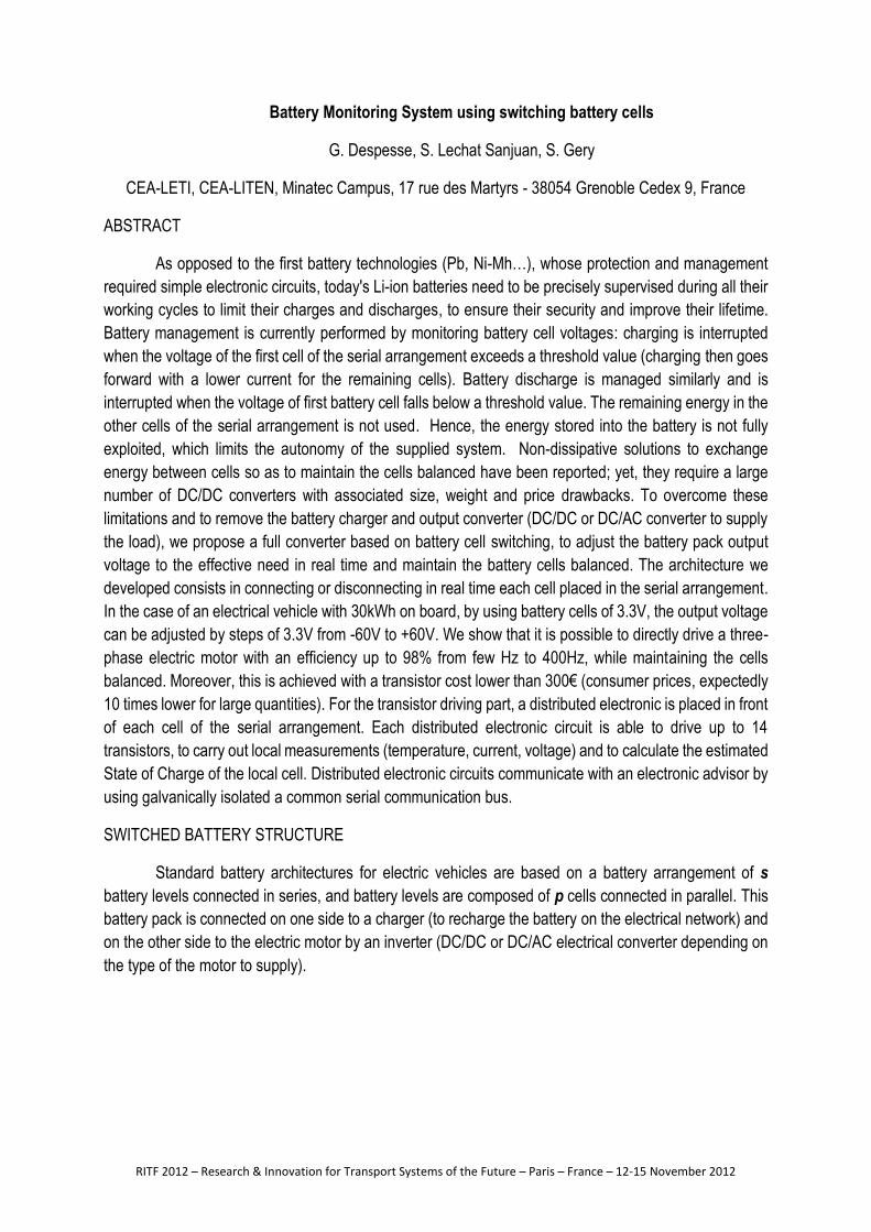
SWITCHED BATTERY STRUCTURE
Standard battery architectures for electric vehicles are based on a battery arrangement of s
battery levels connected in series, and battery levels are composed of p cells connected in parallel. This
battery pack is connected on one side to a charger (to recharge the battery on the electrical network) and
on the other side to the electric motor by an inverter (DC/DC or DC/AC electrical converter depending on
the type of the motor to supply).
RITF 2012 – Research & Innovation for Transport Systems of the Future – Paris – France – 12-15 November 2012
Figure 1 : Standard architecture around the battery pack
In typical applications, the number s of cells placed in series ranges from 15 (≈48V on DC bus) to few
hundreds (up to 900 V on DC bus).
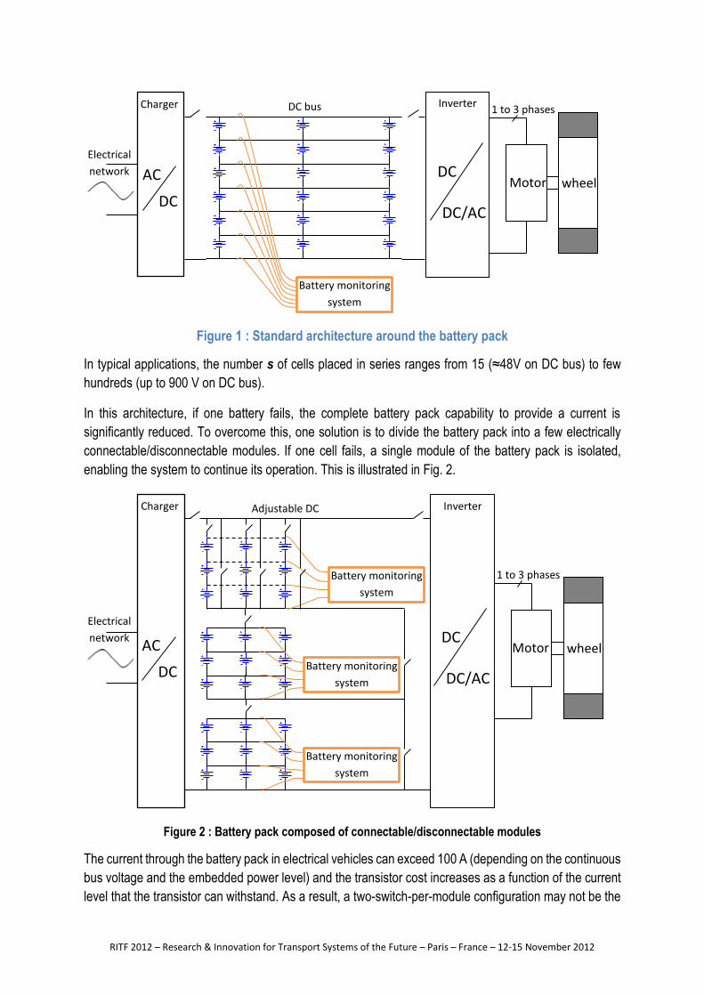
In this architecture, if one battery fails, the complete battery pack capability to provide a current is
significantly reduced. To overcome this, one solution is to divide the battery pack into a few electrically
connectable/disconnectable modules. If one cell fails, a single module of the battery pack is isolated,
enabling the system to continue its operation. This is illustrated in Fig. 2.
Figure 2 : Battery pack composed of connectable/disconnectable modules
The current through the battery pack in electrical vehicles can exceed 100 A (depending on the continuous
bus voltage and the embedded power level) and the transistor cost increases as a function of the current
level that the transistor can withstand. As a result, a two-switch-per-module configuration may not be the
DC
DC/AC
Motor wheel
1 to 3 phases
AC
DC
Electrical
network
DC bus Charger Inverter
Battery monitoring
system
DC
DC/AC
Motor wheel
1 to 3 phases
AC
DC
Electrical
network
Adjustable DC
bus
Charger Inverter
Battery monitoring
system
Battery monitoring
system
Battery monitoring
system
RITF 2012 – Research & Innovation for Transport Systems of the Future – Paris – France – 12-15 November 2012
most suitable option. At constant price and constant losses, it is interesting to decrease the transistor size
and increase the number of transistors, which in addition multiplies the physical dissipating points and
decreases the losses on each point, making it easier to maintain the temperature of the system without
any costly and heavy radiators. Multiplying the number of transistors also ensures redundancy, which
increases security and shortens electrical connections (one does not need to concentrate the whole
current in one transistor and redistribute it afterwards). Transistor multiplication can be implemented as
represented on the upper module of Figure 2. This enables module division into several commutable
columns and single module subpart isolation.
The number of serial cells to be placed in each module is mainly related to the voltages that the transistors
can support. Transistor cost is proportional to its maximum voltage. It is thus suitable to divide the battery
pack into many small voltage modules in order to improve the battery granularity. An optimum module
voltage is around 25V, since below this limit, the individual transistor cost is no longer proportional to the
voltage and becomes constant. 25V are equivalent to 4 or 5 serial battery cells depending on their
maximum voltage. This module voltage is close to the standard maximum MOSFET gate-source voltage
Vgs and hence easily drivable. Furthermore, small voltage modules enable to reduce voltage slew rates
and corresponding electromagnetic perturbations during transistor transitions.
With the optimal module size in terms of transistor cost sorted, the system now requires a Battery
Monitoring System (BMS) in each module (to ensure cell balancing inside each module), a charger and
an inverter. The cell balancing circuit can be replaced by single-serial-cell modules, cell balancing thus
proceeding by using more often the modules having higher States of Charge and less often the modules
having lower States of Charge. With such modules, the output voltage can be adjusted by steps of a single
battery cell voltage (3.2V/3.6V for Li-ion battery). By dynamically switching the modules, it becomes
possible to produce a near-perfect sinusoidal waveform that can directly drive an electrical motor. As the
output voltage step is lower than the resistive voltage drop in classical electric chains, one can also directly
recharge the battery pack on the electrical network without any or with a very low size inductor. In
conclusion, dynamic switching of the modules would enable to get rid of the costly inverter and its cooling
system, the costly and heavy capacitor placed before the inverter to filter the current, the costly and heavy
charger and the costly converter placed in the rapid charging stations. Furthermore, as the battery cell
voltages tend to increase with the new battery technologies and the power transistor voltages tend to
decrease with the transistors gate length reduction, there is a good chance that in the near future, optimal
cost architectures will indeed tend towards modules of only one serial cell.
The objectives of this work are (i) to evaluate the feasibility of completely replacing the charger, the
inverter and the battery cell balancing by module dynamic switching, (ii) to estimate the effects on the
global structure and (iii) to identify the main challenges of implementing such a solution. Two prototypes
have been fabricated to validate this principle, as described below.
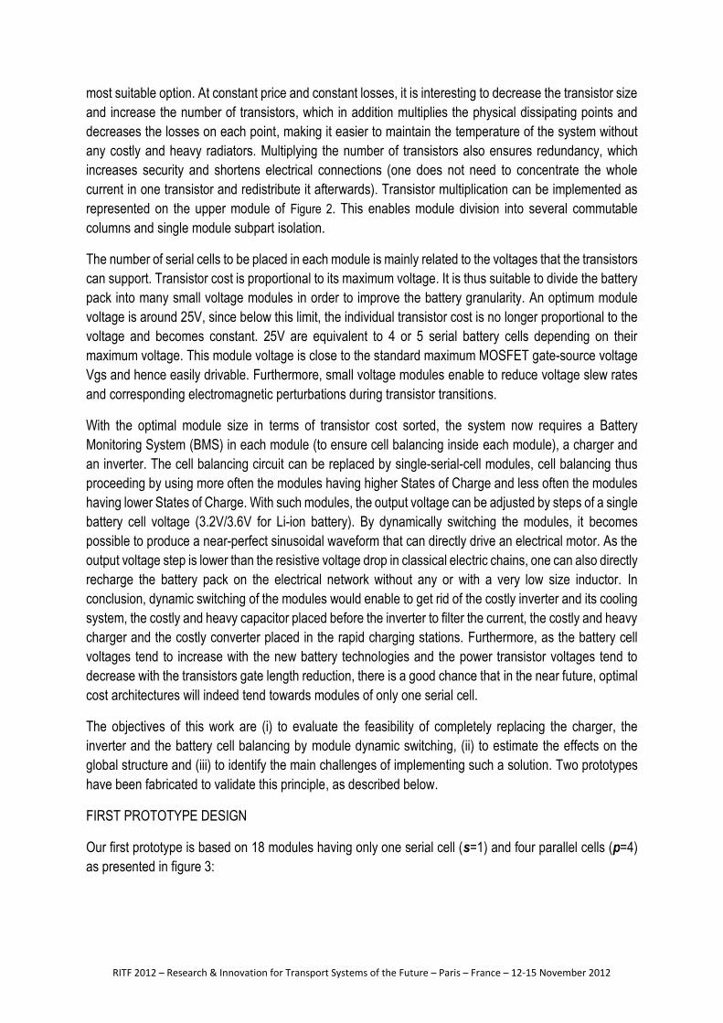
FIRST PROTOTYPE DESIGN
Our first prototype is based on 18 modules having only one serial cell (s=1) and four parallel cells (p=4)
as presented in figure 3:
RITF 2012 – Research & Innovation for Transport Systems of the Future – Paris – France – 12-15 November 2012
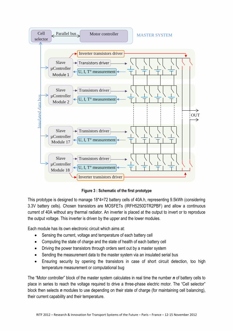
Figure 3 : Schematic of the first prototype
This prototype is designed to manage 18*4=72 battery cells of 40A.h, representing 9.5kWh (considering
3.3V battery cells). Chosen transistors are MOSFETs (IRFH5250DTR2PBF) and allow a continuous
current of 40A without any thermal radiator. An inverter is placed at the output to invert or to reproduce
the output voltage. This inverter is driven by the upper and the lower modules.
Each module has its own electronic circuit which aims at:
Sensing the current, voltage and temperature of each battery cell
Computing the state of charge and the state of health of each battery cell
Driving the power transistors through orders sent out by a master system
Sending the measurement data to the master system via an insulated serial bus
Ensuring security by opening the transistors in case of short circuit detection, too high
temperature measurement or computational bug
The “Motor controller” block of the master system calculates in real time the number n of battery cells to
place in series to reach the voltage required to drive a three-phase electric motor. The “Cell selector”
block then selects n modules to use depending on their state of charge (for maintaining cell balancing),
their current capability and their temperature.
Transistors driver
Inverter transistors driver
U, I, T° measurement
Slave
µController
Module 1
Cell
selector Motor controller Parallel bus
Transistors driver
U, I, T° measurement
Slave
µController
Module 2
Transistors driver
U, I, T° measurement
Slave
µController
Module 17
Transistors driver
U, I, T° measurement
Slave
µController
Module 18
Inverter transistors driver
OUT
MASTER SYSTEM In
sula
ted d
ata
bus
RITF 2012 – Research & Innovation for Transport Systems of the Future – Paris – France – 12-15 November 2012
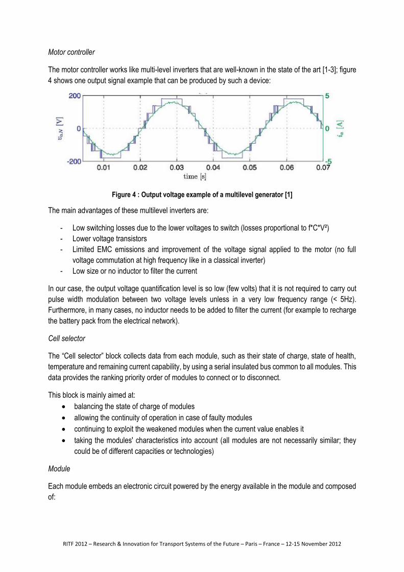
Motor controller
The motor controller works like multi-level inverters that are well-known in the state of the art [1-3]; figure
4 shows one output signal example that can be produced by such a device:
Figure 4 : Output voltage example of a multilevel generator [1]
The main advantages of these multilevel inverters are:
- Low switching losses due to the lower voltages to switch (losses proportional to f*C*V²)
- Lower voltage transistors
- Limited EMC emissions and improvement of the voltage signal applied to the motor (no full
voltage commutation at high frequency like in a classical inverter)
- Low size or no inductor to filter the current
In our case, the output voltage quantification level is so low (few volts) that it is not required to carry out
pulse width modulation between two voltage levels unless in a very low frequency range (< 5Hz).
Furthermore, in many cases, no inductor needs to be added to filter the current (for example to recharge
the battery pack from the electrical network).
Cell selector
The “Cell selector” block collects data from each module, such as their state of charge, state of health,
temperature and remaining current capability, by using a serial insulated bus common to all modules. This
data provides the ranking priority order of modules to connect or to disconnect.
This block is mainly aimed at:
balancing the state of charge of modules
allowing the continuity of operation in case of faulty modules
continuing to exploit the weakened modules when the current value enables it
taking the modules' characteristics into account (all modules are not necessarily similar; they
could be of different capacities or technologies)
Module
Each module embeds an electronic circuit powered by the energy available in the module and composed
of:
RITF 2012 – Research & Innovation for Transport Systems of the Future – Paris – France – 12-15 November 2012
a micro-controller to decode orders from the master system, synthesize measurements, compute
the states of charge, arbitrate the cells to use in the module, ensure security with extreme
temperatures, currents and voltages
a serial communication interface to communicate with the master system: the estimation of the
module states is performed within the module and transmitted to the master system, which then
computes the future configuration of the module (connection or disconnection) and transmits the
order to it
a measurement interface to sense the current, temperature and voltage of each cell
a discreet logic circuit to open the shunt or serial transistors in case of short circuit or transistor
failure detection
a power driver interface to drive the 8 or 10 transistors of the module; this driver is able to
command each transistor with 20V in less than 300ns
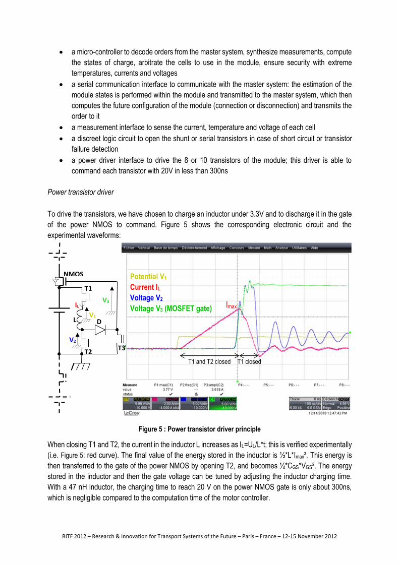
Power transistor driver
To drive the transistors, we have chosen to charge an inductor under 3.3V and to discharge it in the gate
of the power NMOS to command. Figure 5 shows the corresponding electronic circuit and the
experimental waveforms:
Figure 5 : Power transistor driver principle
When closing T1 and T2, the current in the inductor L increases as IL=UL/L*t; this is verified experimentally
(i.e. Figure 5: red curve). The final value of the energy stored in the inductor is ½*L*Imax². This energy is
then transferred to the gate of the power NMOS by opening T2, and becomes ½*CGS*VGS². The energy
stored in the inductor and then the gate voltage can be tuned by adjusting the inductor charging time.
With a 47 nH inductor, the charging time to reach 20 V on the power NMOS gate is only about 300ns,
which is negligible compared to the computation time of the motor controller.
Potential V1
Current IL
Voltage V2
Voltage V3 (MOSFET gate)
NMOS
V2
T1
T2
L D
T3
V1
V3 IL
T1 and T2 closed T1 closed
Imax
RITF 2012 – Research & Innovation for Transport Systems of the Future – Paris – France – 12-15 November 2012
If the NMOS command has to be maintained on its “on” state for more than 1ms, then a new energy pulse
is sent to the NMOS gate every 1ms.
The NMOS is open by opening T1 and closing T3 which discharges the NMOS gate.
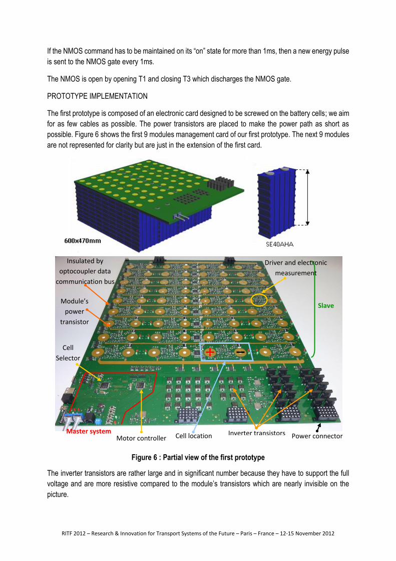
PROTOTYPE IMPLEMENTATION
The first prototype is composed of an electronic card designed to be screwed on the battery cells; we aim
for as few cables as possible. The power transistors are placed to make the power path as short as
possible. Figure 6 shows the first 9 modules management card of our first prototype. The next 9 modules
are not represented for clarity but are just in the extension of the first card.
Figure 6 : Partial view of the first prototype
The inverter transistors are rather large and in significant number because they have to support the full
voltage and are more resistive compared to the module’s transistors which are nearly invisible on the
picture.
Slave
s
Master system
Cell
Selector
Motor controller
Insulated by
optocoupler data
communication bus
Cell location Inverter transistors Power connector
Driver and electronic
measurement
Module’s
power
transistor
RITF 2012 – Research & Innovation for Transport Systems of the Future – Paris – France – 12-15 November 2012
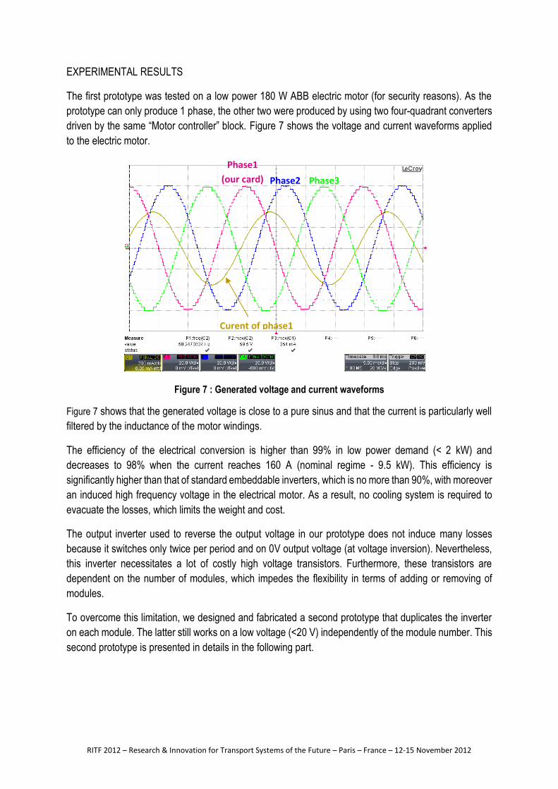
EXPERIMENTAL RESULTS
The first prototype was tested on a low power 180 W ABB electric motor (for security reasons). As the
prototype can only produce 1 phase, the other two were produced by using two four-quadrant converters
driven by the same “Motor controller” block. Figure 7 shows the voltage and current waveforms applied
to the electric motor.
Figure 7 : Generated voltage and current waveforms
Figure 7 shows that the generated voltage is close to a pure sinus and that the current is particularly well
filtered by the inductance of the motor windings.
The efficiency of the electrical conversion is higher than 99% in low power demand (< 2 kW) and
decreases to 98% when the current reaches 160 A (nominal regime - 9.5 kW). This efficiency is
significantly higher than that of standard embeddable inverters, which is no more than 90%, with moreover
an induced high frequency voltage in the electrical motor. As a result, no cooling system is required to
evacuate the losses, which limits the weight and cost.
The output inverter used to reverse the output voltage in our prototype does not induce many losses
because it switches only twice per period and on 0V output voltage (at voltage inversion). Nevertheless,
this inverter necessitates a lot of costly high voltage transistors. Furthermore, these transistors are
dependent on the number of modules, which impedes the flexibility in terms of adding or removing of
modules.
To overcome this limitation, we designed and fabricated a second prototype that duplicates the inverter
on each module. The latter still works on a low voltage (<20 V) independently of the module number. This
second prototype is presented in details in the following part.
Phase1
(our card) Phase2 Phase3
Curent of phase1
RITF 2012 – Research & Innovation for Transport Systems of the Future – Paris – France – 12-15 November 2012
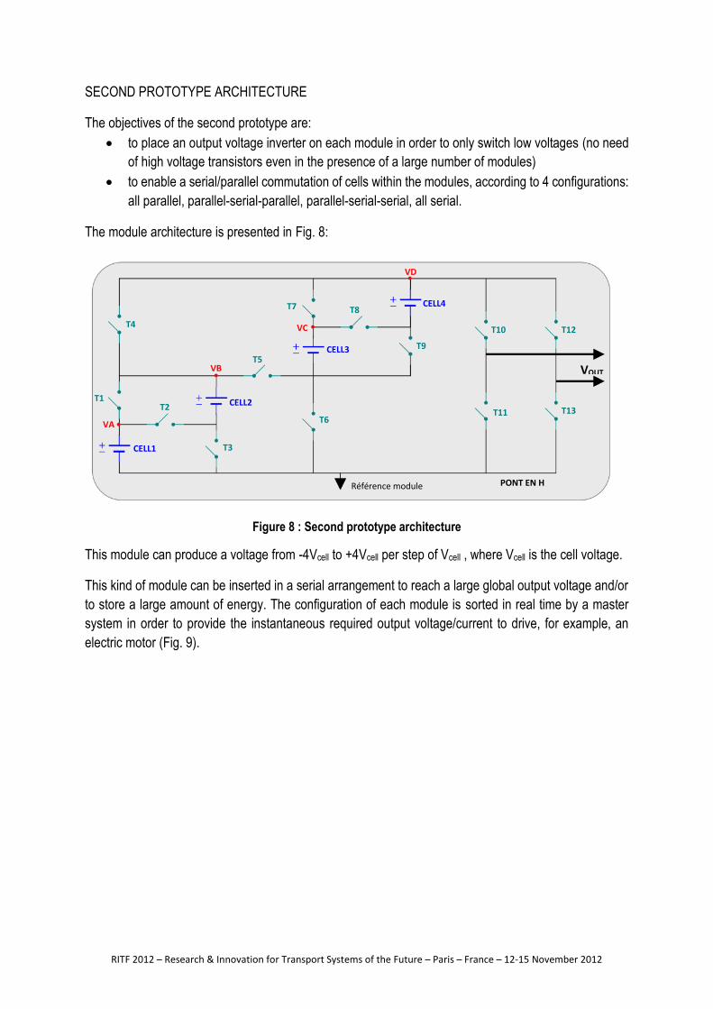
SECOND PROTOTYPE ARCHITECTURE
The objectives of the second prototype are:
to place an output voltage inverter on each module in order to only switch low voltages (no need
of high voltage transistors even in the presence of a large number of modules)
to enable a serial/parallel commutation of cells within the modules, according to 4 configurations:
all parallel, parallel-serial-parallel, parallel-serial-serial, all serial.
The module architecture is presented in Fig. 8:
Figure 8 : Second prototype architecture
This module can produce a voltage from -4Vcell to +4Vcell per step of Vcell , where Vcell is the cell voltage.
This kind of module can be inserted in a serial arrangement to reach a large global output voltage and/or
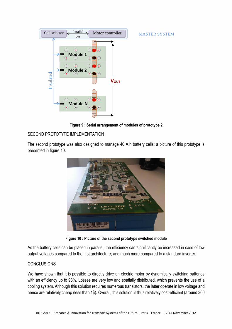
to store a large amount of energy. The configuration of each module is sorted in real time by a master
system in order to provide the instantaneous required output voltage/current to drive, for example, an
electric motor (Fig. 9).
CELL1
CELL2
CELL3
CELL4
PONT EN H Référence module
T1 T2
T3
T4
T5
T6
T7 T8
T9
T10
T11
T12
T13
VOUT
VA
VB
VC
VD
RITF 2012 – Research & Innovation for Transport Systems of the Future – Paris – France – 12-15 November 2012
Figure 9 : Serial arrangement of modules of prototype 2
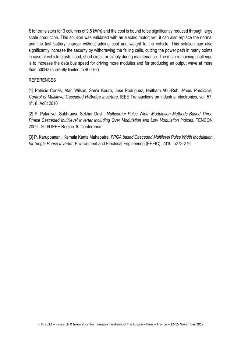
SECOND PROTOTYPE IMPLEMENTATION
The second prototype was also designed to manage 40 A.h battery cells; a picture of this prototype is
presented in figure 10.
Figure 10 : Picture of the second prototype switched module
As the battery cells can be placed in parallel, the efficiency can significantly be increased in case of low
output voltages compared to the first architecture; and much more compared to a standard inverter.
CONCLUSIONS
We have shown that it is possible to directly drive an electric motor by dynamically switching batteries
with an efficiency up to 98%. Losses are very low and spatially distributed, which prevents the use of a
cooling system. Although this solution requires numerous transistors, the latter operate in low voltage and
hence are relatively cheap (less than 1$). Overall, this solution is thus relatively cost-efficient (around 300
VOUT
Module 1
Module 2
Module N
…
Cell selector Motor controller Parallel
bus MASTER SYSTEM
Insu
late
d
dat
a bus
RITF 2012 – Research & Innovation for Transport Systems of the Future – Paris – France – 12-15 November 2012
€ for transistors for 3 columns of 9.5 kWh) and the cost is bound to be significantly reduced through large
scale production. This solution was validated with an electric motor; yet, it can also replace the normal
and the fast battery charger without adding cost and weight to the vehicle. This solution can also
significantly increase the security by withdrawing the failing cells, cutting the power path in many points
in case of vehicle crash, flood, short circuit or simply during maintenance. The main remaining challenge
is to increase the data bus speed for driving more modules and for producing an output wave at more
than 500Hz (currently limited to 400 Hz).
REFERENCES
[1] Patricio Cortés, Alan Wilson, Samir Kouro, Jose Rodriguez, Haitham Abu-Rub, Model Predictive,
Control of Multilevel Cascaded H-Bridge Inverters, IEEE Transactions on industrial electronics, vol. 57,
n°. 8, Août 2010
[2] P. Palanivel, Subhransu Sekhar Dash, Multicarrier Pulse Width Modulation Methods Based Three
Phase Cascaded Multilevel Inverter Including Over Modulation and Low Modulation Indices, TENCON
2009 - 2009 IEEE Region 10 Conference
[3] P. Karuppanan, Kamala Kanta Mahapatra, FPGA based Cascaded Multilevel Pulse Width Modulation
for Single Phase Inverter, Environment and Electrical Engineering (EEEIC), 2010, p273-276