Embed Size (px)
Citation preview
Benefit of ArF immersion lithography in 55 nm logic device manufacturing
Takayuki Uchiyama*a, Takao Tamura a, Kazuyuki Yoshimochi a,
Paul Graupner b, Hans Bakker c, Eelco van Setten c, Kenji Morisaki d, a NEC Electronics Corporation, 1120 Shimokuzawa, Sagamihara, Kanagawa, Japan, 229-1198;
b Carl Zeiss, Semiconductor Manufacturing Technology AG, 73447 Oberkochen, Germany;
c ASML, De Run 6501, DR Veldhoven, The Netherlands; d ASML Japan, 2-15-1 Konan, Minato-ku, Tokyo 108-6022, Japan
ABSTRACT
In this paper we demonstrate the many benefits of using immersion lithography that go beyond depth of focus (DOF) improvement by comparing several key features of dry and immersion lithography. Immersion lithography improves critical dimension uniformity (CDU) as well as avoiding the necessity for strong resolution enhancement techniques (RET) as compared with dry lithography. Thus it is possible to significantly reduce the burden of optical proximity correction (OPC) work with immersion lithography. With respect to imaging, we studied the sensitivity of the lithographic performances to aberrations and light source spectral bandwidth E95 fluctuations to highlight the benefits of immersion lithography. The significant improvements that have been seen in the last year in overlay accuracy, defect control and focus & leveling accuracy have been considered to be challenges to the realization of immersion lithography in mass production. Now these challenges have been met for the manufacturing requirements of 55 nm logic devices. The achievements of immersion lithography include overlay accuracy within 10 nm on resist-to-resist wafers and within 20 nm on production wafers, fewer than 10 defects per wafer, and errors of less than 40 nm in focus & leveling on full wafers. We have established a top-coat resist process. In conclusion, immersion lithography is the most promising manufacturing solution for 55 nm node logic devices, providing advantages in CDU control, and equivalent overlay performance and focus & leveling accuracy to dry ArF, without an increased level of defects. NEC Electronics has completed development and preproduction of the 55 nm logic device “UX7LS” using immersion lithography and has established the lithography technology for mass production of the UX7LS this year.
Keywords: Immersion lithography, 55nm logic device, Imaging, Overlay, CD uniformity
1. INTRODUCTION ArF immersion lithography is the technology that will follow dry ArF, leading to smaller devices in the future, at the 65 nm node and below1-13. This technology is ready for mass production, as immersion exposure tools with a numerical aperture (NA) larger than 1.0 have started to be shipped. Many technological challenges had to be overcome to bring about immersion lithography for mass production, but those challenges have been met.
In this paper, we discuss the current status of immersion lithography, focusing on the pros and cons of its introduction to a mass production environment, especially for lower NA (NA<1.0) applications by comparative factor analysis of several lithographic performance errors.
The key challenges in ArF immersion are defectivity and overlay control. There are several concerns in the immersion process such as tool contamination and/or defects due to leaching from the resist material, pattern defects, and resist profile degradation due to water droplets. Thus immersion hood improvements and a hydrophobic topcoat have been introduced. Also, overlay accuracy degradation due to water evaporation is a concern as it can cause wafer temperature instability during exposure. We have confirmed that overlay performance is well controlled by having a wafer table temperature control system in the exposure tool.
0.78
0.81
0.84
0.87 0.9
0.93
0.7
0.75
0.8
0.85
0.9
NA
σ
0.78
0.81
0.84
0.87 0.9
0.93
0.7
0.75
0.8
0.85
0.9
NA
σ
Wet Dry
With respect to imaging performance, DOF improvement with immersion lithography is well known. Recently the burden of OPC work for ASIC devices has become a more serious issue. Reduction in the burden of OPC work is a significant benefit of immersion lithography, as the use of strong RETS can be avoided due to improved DOF.
In this paper, we will highlight the advantages of immersion lithography by contrasting it with dry lithography for 55 nm logic device patterns with respect to robustness against imaging errors, and sensitivity to aberrations and to E95 fluctuation under optimum optical conditions. Also, we will show that overlay, focus and defect control of immersion lithography meet the requirements for 55 nm logic device manufacture due to significant improvements in the past year. Finally, we will discuss the status of immersion lithography as applied to the UX7LS 55 nm logic device by NEC Electronics.
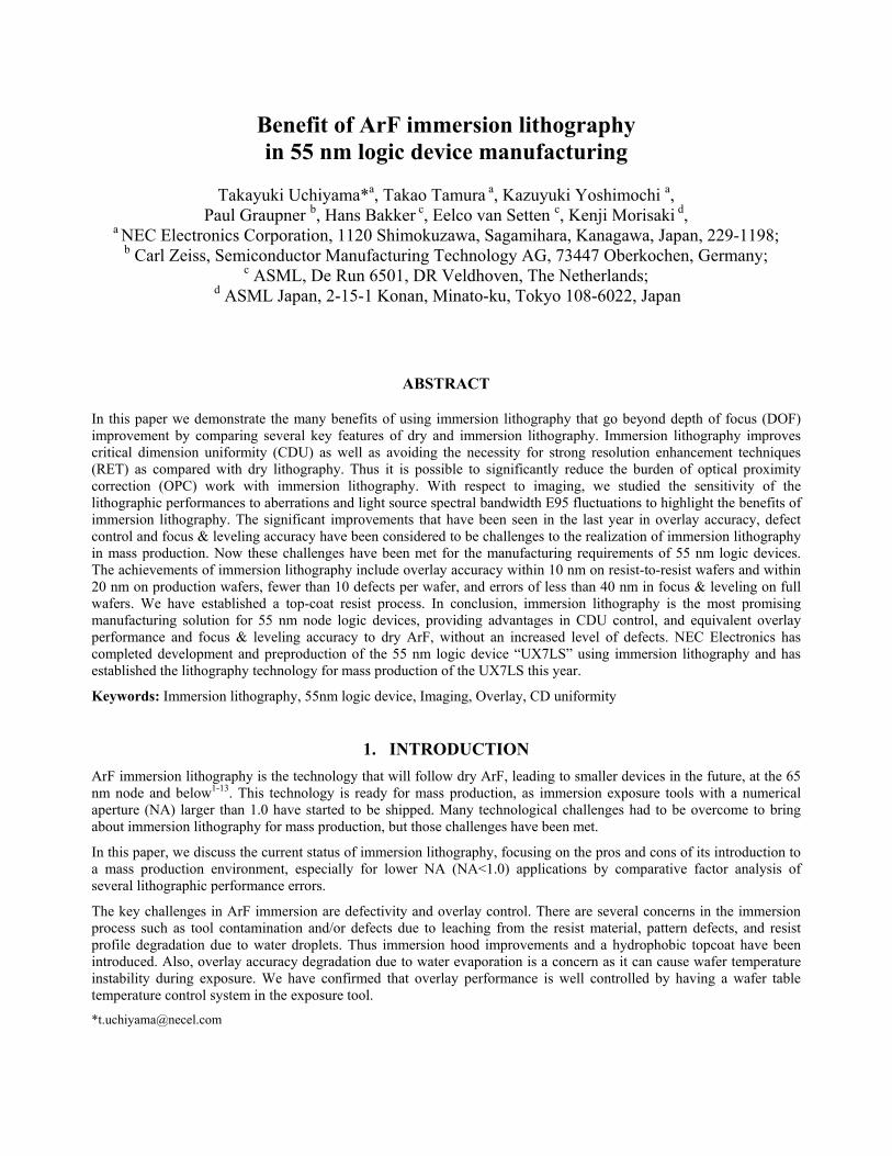
2. IMAGING PERFORMANCE COMPARISON Optical conditions for an 80 nm line pattern were optimized for both immersion and dry lithography. Simulation was done assuming a gate layer for a 55 nm logic device. CDUs were calculated with each error factor, assuming conventional illumination with Att-PSM, annular illumination with attenuated phase shift mask (Att-PSM) and conventional illumination with alternated phase shift mask (Alt -PSM). It was assumed that the NA was smaller than 0.93. The simulation conditions are shown in Table 1, and results in Figure 1a~c.
Table 1 Simulation condition for optimizing NA & Sigma setting Item Conditions Simulation mode Vector mode CD light intensity threshold NA 0.78~0.93, dry & wet(n=1.44) Partial coherence (sigma)
0.70~0.90@Conv.+AttPSM (6%) Outer sigma=0.75~0.90@2/3 Annular + AttPSM (6%) 0.3~0.45@Conv.+Alt-PSM
Pattern 80nm L&S, pitch=2000nm, 240nm, 180nm Error Mask error=+/-2nm
Dose error=+/-1.2% Focus error=+/-50nm Flare=1% (fixed)
Figure 1a CDU Map of Conv. + Att-PSM
0.78
0.81
0.84
0.87 0.9
0.93
0.75
0.8
0.85
0.9
NA
σ
0.78
0.81
0.84
0.87 0.9
0.93
0.75
0.8
0.85
0.9
NA
σ
Wet Dry
0.78
0.81
0.84
0.87 0.9
0.93
0.3
0.35
0.4
0.45
NA
σ
0.78
0.81
0.84
0.87 0.9
0.93
0.3
0.35
0.4
0.45
NA
σ
Wet Dry
0
5
10
15
CDU
(nm
)
Wet Dry
0.93
/0.8
0 Co
nv.
0.93
/0.7
5 An
nula
r
0.93
/0.3
0 al
t-PS
M
0.90
/0.8
0 Co
nv.
0.87
/0.7
5 An
nula
r
0.93
/0.3
0 al
t-PS
M
8.7 8.0 5.7 12.6 11.1 9.9
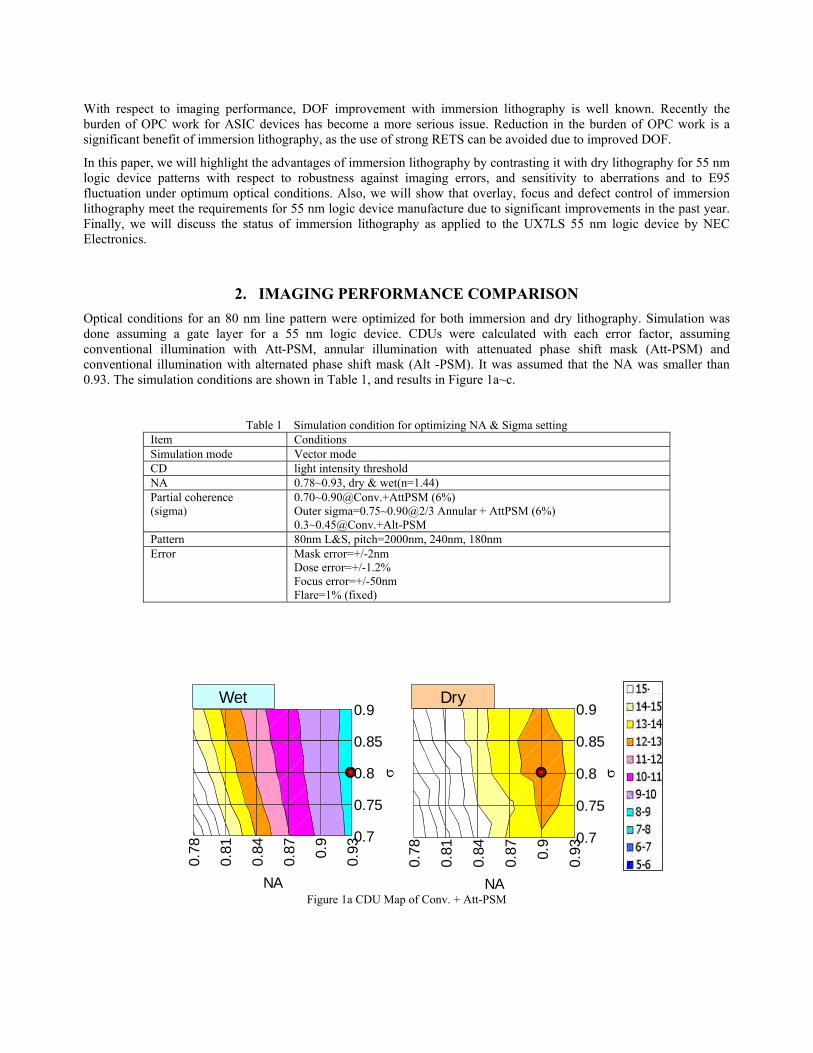
Figure 1b CDU Map of Annular + Att-PSM
Figure 1c CDU Map of Conv. + Alt-PSM Figure 2a shows a summary of CDUs for each optimum NA and sigma setting. It was found that immersion lithography gave better CDU than dry when the same exposure method was used. Dry lithography using Alt-PSM could not give better CDU than immersion lithography using conventional illumination. Therefore, a strong RET was not required for immersion lithography to achieve the same CDU as dry lithography.
Figure 2a Optimized NA and sigma setting and CDU
00.10.20.30.40.50.60.70.80.9
1
180n
m
240n
m
2000
nm
180n
m
240n
m
2000
nm
180n
m
240n
m
2000
nm
180n
m
240n
m
2000
nm
180n
m
240n
m
2000
nm
180n
m
240n
m
2000
nm
Sens
itivi
ty (
nm/n
m_i
n_Ze
rnik
e)
Z9Z16
Wet Dry
WC WA WL DC DA DL
pitc
h
00.10.20.30.40.50.60.70.80.9
1
180n
m
240n
m
2000
nm
180n
m
240n
m
2000
nm
180n
m
240n
m
2000
nm
180n
m
240n
m
2000
nm
180n
m
240n
m
2000
nm
180n
m
240n
m
2000
nm
Sens
itivi
ty (
nm/n
m_i
n_Ze
rnik
e)
Z9Z16
Wet Dry
WC WA WL DC DA DL
00.10.20.30.40.50.60.70.80.9
1
180n
m
240n
m
2000
nm
180n
m
240n
m
2000
nm
180n
m
240n
m
2000
nm
180n
m
240n
m
2000
nm
180n
m
240n
m
2000
nm
180n
m
240n
m
2000
nm
Sens
itivi
ty (
nm/n
m_i
n_Ze
rnik
e)
Z9Z16
Wet Dry
WC WA WL DC DA DL
pitc
h
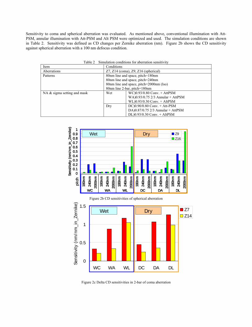
Sensitivity to coma and spherical aberration was evaluated. As mentioned above, conventional illumination with Att-PSM, annular illumination with Att-PSM and Alt PSM were optimized and used. The simulation conditions are shown in Table 2. Sensitivity was defined as CD changes per Zernike aberration (nm). Figure 2b shows the CD sensitivity against spherical aberration with a 100 nm defocus condition.
Table 2 Simulation conditions for aberration sensitivity Item Conditions Aberrations Z7, Z14 (coma), Z9, Z16 (spherical) Patterns 80nm line and space, pitch=180nm
80nm line and space, pitch=240nm 80nm line and space, pitch=2000nm (Iso) 80nm line 2-bar, pitch=180nm Wet
WC)0.93/0.80 Conv. + AttPSM WA)0.93/0.75 2/3 Annular + AttPSM WL)0.93/0.30 Conv. + AltPSM
NA & sigma setting and mask
Dry
DC)0.90/0.80 Conv. + Att-PSM DA)0.87/0.75 2/3 Annular + AttPSM DL)0.93/0.30 Conv. + AltPSM
Figure 2b CD sensitivities of spherical aberration
Figure 2c Delta CD sensitivities in 2-bar of coma aberration
0
0.5
1
1.5
WC WA WL DC DA DL
Sens
itivi
ty (
nm/n
m_i
n_Ze
rnik
e)
Z7Z14
Wet Dry
0
0.2
0.4
0.6
0.8
1
1.2
1.418
0nm
240n
m
2000
nm
180n
m
240n
m
2000
nm
180n
m
240n
m
2000
nm
180n
m
240n
m
2000
nm
180n
m
240n
m
2000
nm
180n
m
240n
m
2000
nm
Sens
itivi
ty (
nm/n
m_i
n_Ze
rnik
e)
Z7Z14
Wet Dry
WC WA WL DC DA DL
pitc
h
0
0.2
0.4
0.6
0.8
1
1.2
1.418
0nm
240n
m
2000
nm
180n
m
240n
m
2000
nm
180n
m
240n
m
2000
nm
180n
m
240n
m
2000
nm
180n
m
240n
m
2000
nm
180n
m
240n
m
2000
nm
Sens
itivi
ty (
nm/n
m_i
n_Ze
rnik
e)
Z7Z14
Wet Dry
WC WA WL DC DA DL
pitc
h
0
0.5
1
1.5
2
2.5
180n
m
240n
m
2000
nm
180n
m
240n
m
2000
nm
180n
m
240n
m
2000
nm
180n
m
240n
m
2000
nm
180n
m
240n
m
2000
nm
180n
m
240n
m
2000
nm
Sens
itivi
ty (
nm/[
sigm
a er
ror(
%)]
)
Wet Dry
WC WA WL DC DA DL
pitc
h
0
0.5
1
1.5
2
2.5
180n
m
240n
m
2000
nm
180n
m
240n
m
2000
nm
180n
m
240n
m
2000
nm
180n
m
240n
m
2000
nm
180n
m
240n
m
2000
nm
180n
m
240n
m
2000
nm
Sens
itivi
ty (
nm/[
sigm
a er
ror(
%)]
)
Wet Dry
WC WA WL DC DA DL
pitc
h
Wet Dry
WC WA WL DC DA DL
pitc
h
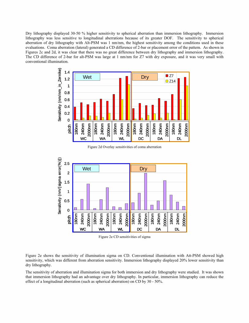
Dry lithography displayed 30-50 % higher sensitivity to spherical aberration than immersion lithography. Immersion lithography was less sensitive to longitudinal aberrations because of its greater DOF. The sensitivity to spherical aberration of dry lithography with Alt-PSM was 1 nm/nm, the highest sensitivity among the conditions used in these evaluations. Coma aberration (lateral) generated a CD difference of 2-bar or placement error of the pattern. As shown in Figures 2c and 2d, it was clear that there was no great difference between dry lithography and immersion lithography. The CD difference of 2-bar for alt-PSM was large at 1 nm/nm for Z7 with dry exposure, and it was very small with conventional illumination.
Figure 2d Overlay sensitivities of coma aberration
Figure 2e CD sensitivities of sigma
Figure 2e shows the sensitivity of illumination sigma on CD. Conventional illumination with Att-PSM showed high sensitivity, which was different from aberration sensitivity. Immersion lithography displayed 20% lower sensitivity than dry lithography.
The sensitivity of aberration and illumination sigma for both immersion and dry lithography were studied. It was shown that immersion lithography had an advantage over dry lithography. In particular, immersion lithography can reduce the effect of a longitudinal aberration (such as spherical aberration) on CD by 30 - 50%.

Wet1400i(wet:WC)
Dry1400(dry:DC)
65
70
75
80
85
0 500 1000 1500 2000
Pattern pitch (nm)
CD
(nm
)
0.30.50.7
65
70
75
80
85
0 500 1000 1500 2000
Pattern pitch (nm)
CD
(nm
)
0.30.50.7
Figure 2f OPE curve sensitivity of spectral width E95 in case of Conv. + Att-PSM)
Figure 2g CD sensitivity of spectral width E95
The impact of the laser bandwidth E95 of the ArF excimer laser illumination source was also studied. The CD change of an 80 nm line pattern with 240 nm pitch and 2000 nm pitch was calculated with E95s of 0.3 - 0.7 pm under the given conditions of NA and sigma and shown in Table 2. Exposure was appropriate for an 80 nm line with 180 nm pitch printed onto 80 nm. Figure 2f shows an OPE curve under conventional illumination with Att-PSM. It was found that the effect of E95 on CD using immersion lithography is 20 - 30% smaller than with dry lithography (Figure 2g). The spectrum width of the light source caused chromatic aberration and reduced the image contrast through imperfect focus. Thus immersion lithography had an advantage because of its greater DOF.
3. SCANNER PERFORMANCE COMPARISON In immersion lithography, filling the gap between the bottom lens of the projection optics and the wafer with water of refractive index 1.44 makes the incidence angle smaller and increases DOF by a factor of approximately 1.4, and can produce the effect of a NA greater than 1. In the partial-fill method, water is introduced only into the gap between the lens and wafer, to avoid leaving a water droplet behind on the wafer when the exposure is completed. Furthermore, there is a temperature control function in each part to compensate for temperature change due to water evaporation and prevent wafer deformation from causing overlay problems or focus instability to the extent possible8.
In the past year, the overlay performance of immersion lithography has shown drastic improvement. Figure 3a shows the improvement of XT:1400Ei (ArF immersion) overlay performance. An 8 nm level was achieved in SMO under the present conditions, confirmed to be the same level of performance as with dry ArF for an XT:1400 (less than 8 nm).
0
0.5
1
1.5
2
WC WA WL DC DA DL
Sens
itivi
ty (
nm/0
.1pm
_in_
E95)
Wet Dry
0.0
5.0
10.0
15.0
20.0
25.0
30.0
2005
/10/
30
2005
/11/
30
2005
/12/
30
2006
/1/3
0
2006
/2/2
8
2006
/3/3
0
2006
/4/3
0
2006
/5/3
0
2006
/6/3
0
2006
/7/3
0
2006
/8/3
0
2006
/9/3
0
2006
/10/
30
2006
/11/
30
2006
/12/
30
2007
/1/3
0
2007
/2/2
8
Ove
rlay
(nm
)>20nm
<20nm
<10nm<15nm
Dry level
2005 2006 2007
0
10
20
30
40
50
1 3 9 11 17 19
Wafer No.
Def
ocus
(nm
)
3sigma|Ave|
Chuck#1: 36nm
Chuck#2: 38nm
100nm
-100nm
-50nm
50nm
0nmChuck#1: 36nm
Chuck#2: 38nm
100nm
-100nm
-50nm
50nm
0nm
100nm
-100nm
-50nm
50nm
0nm
Wet resultMA<2nmMSD<8nm
Dry levelMA<2nmMSD<7nmY
MA ≤ 0.7nmMSD ≤ 5.8nm
XMA ≤ 1.0nm
MSD ≤ 6.9nm
Wet
YMA ≤ 0.7nm
MSD ≤ 5.8nm
XMA ≤ 1.0nm
MSD ≤ 6.9nm
YMA ≤ 0.7nm
MSD ≤ 5.8nm
XMA ≤ 1.0nm
MSD ≤ 6.9nm
Wet
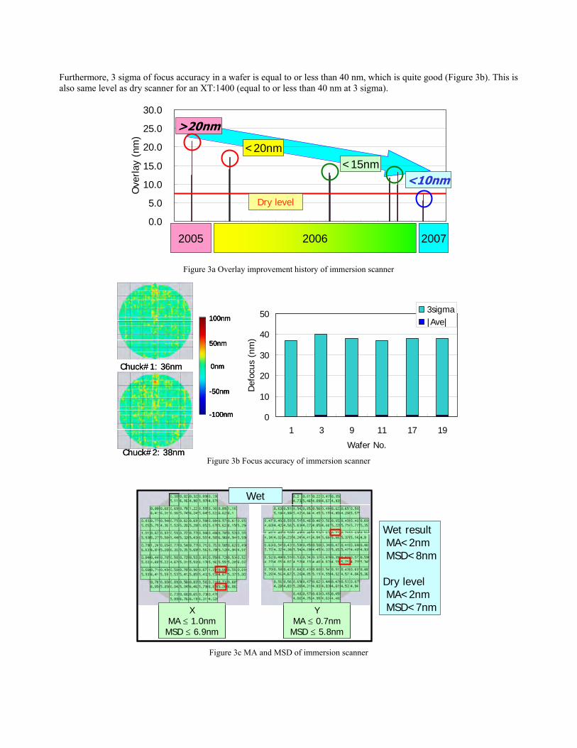
Furthermore, 3 sigma of focus accuracy in a wafer is equal to or less than 40 nm, which is quite good (Figure 3b). This is also same level as dry scanner for an XT:1400 (equal to or less than 40 nm at 3 sigma).
Figure 3a Overlay improvement history of immersion scanner
Figure 3b Focus accuracy of immersion scanner
Figure 3c MA and MSD of immersion scanner
Line patternTotal defect :6
Pattern defect :5Particle:1
Hole patternTotal defect :5
Pattern defect :4Circle defect:1
Line patternTotal defect :6
Pattern defect :5Particle:1
Hole patternTotal defect :5
Pattern defect :4Circle defect:1
Active Gate
Metal1Contact
Active Gate
Metal1Contact
Gate layer
-200 -150 -100 -50 0 50 100 150 200Focus offset (nm)
250nm
-180 -135 -90 -45 0 45 90 135 180
Contact layer
Focus offset (nm)
225nm
Gate layer
-200 -150 -100 -50 0 50 100 150 200Focus offset (nm)
250nmGate layer
-200 -150 -100 -50 0 50 100 150 200Focus offset (nm)
250nm
-180 -135 -90 -45 0 45 90 135 180
Contact layer
Focus offset (nm)
225nm
-180 -135 -90 -45 0 45 90 135 180
Contact layer
Focus offset (nm)
225nm
In immersion lithography the introduction of water and extraction of water and air can cause vibration at the edge of a wafer, leading to problems with scan synchronization. However this was found not to be a problem across the full wafer surface, as shown in Figure 3c for XT:1400Ei. The moving average (MA) of immersion lithography is equal to or less than 2 nm and moving standard deviation (MSD) is equal to or less than 8 nm. MSD is at a level that will produce no problems in imaging performance for a 55 nm logic device even though it is inferior to a dry scanner at levels equal to or less than 7 nm.
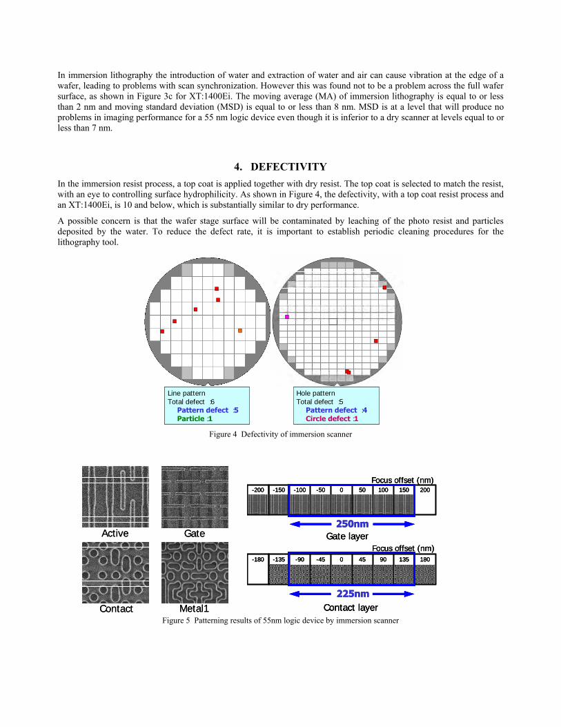
4. DEFECTIVITY In the immersion resist process, a top coat is applied together with dry resist. The top coat is selected to match the resist, with an eye to controlling surface hydrophilicity. As shown in Figure 4, the defectivity, with a top coat resist process and an XT:1400Ei, is 10 and below, which is substantially similar to dry performance.
A possible concern is that the wafer stage surface will be contaminated by leaching of the photo resist and particles deposited by the water. To reduce the defect rate, it is important to establish periodic cleaning procedures for the lithography tool.
Figure 4 Defectivity of immersion scanner
Figure 5 Patterning results of 55nm logic device by immersion scanner

0
10
20
30
40
50
60
0 5 10 15 20Wafer No.
|mea
n| +
3σ[
nm]
|mean|+3σ_X|mean|+3σ_Y
0
10
20
30
40
50
60
0 5 10 15 20 25Wafer No.
|mea
n|+3
σ[n
m]
|mean|+3σ_X|mean|+3σ_Y
0
10
20
30
40
50
60
0 5 10 15 20 25Wafer No.
|mea
n|+3
σ[n
m]
|mean|+3σ_X|mean|+3σ_Y
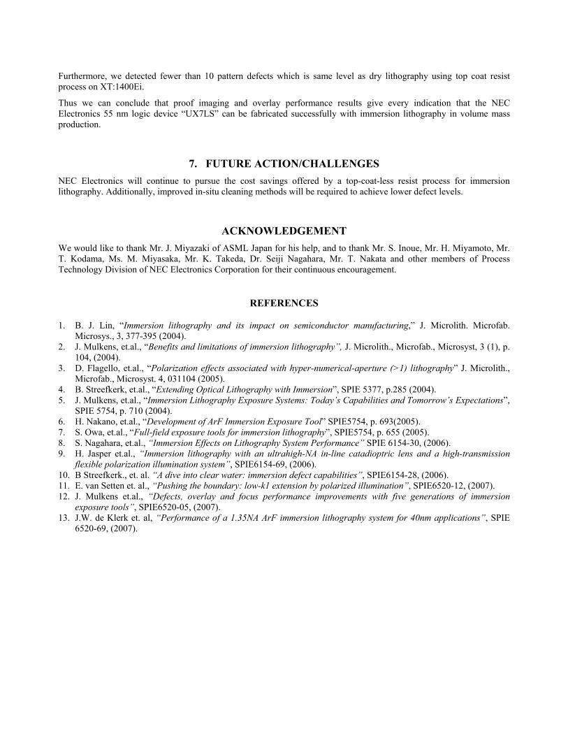
5. 55 NM LOGIC DEVICE EXPOSURE RESULTS The result of immersion lithography for a 55 nm logic device, whose minimum pitch is 180 nm, is shown below. The imaging result for an XT:1400Ei with an NA of 0.93 under conventional illumination is shown in Figure 5. It is clear that a DOF greater than 200 nm was achieved. In addition, the overlay performance of the gate-layer of the 55 nm logic device is shown in Figure 6a, and the Metal-1 layer in Figure 6b. Using a |Mean|+3 sigma definition, X = 15.9 nm, 12.6 nm, and Y = 22 nm, 11.4 nm were achieved, confirming good performance.
Figure 6a Overlay performance of 55nm logic device by immersion scanner, gate to STI
Figure 6b Overlay performance of 55nm logic device by immersion scanner, metal 1 to contact
6. CONCLUSION We have described for the advantages and disadvantages of NA < 1.0 immersion lithography.
Optical image simulation results show that CD uniformity can be improved by using immersion lithography. Strong RETs such as Alt-PSM is not required for immersion lithography to achieve the same CD uniformity as the dry lithography. From a view of sensitivity to lens aberration, immersion lithography reduces sensitivity to spherical aberration by 30-50% (one of the longitudinal aberrations). CD sensitivity to a variation in illumination sigma is 20% better with immersion lithography. Also, sensitivity to E95 laser bandwidth control is improved by 20-30%.
From a machine performance point of view, the overlay accuracy of immersion scanner has been significantly improved in the past year. Current overlay accuracy has reached the 8 nm level, which is almost equal to that of the dry-ArF tool. Focus control variation over the wafer also remains within 40 nm (3 sigma), which is also same level as the dry tool. For scan synchronization, the MA is less than 2 nm, the MSD is less than 8 nm. These key variables are almost identical to those of a dry-ArF exposure.
Furthermore, we detected fewer than 10 pattern defects which is same level as dry lithography using top coat resist process on XT:1400Ei.
Thus we can conclude that proof imaging and overlay performance results give every indication that the NEC Electronics 55 nm logic device “UX7LS” can be fabricated successfully with immersion lithography in volume mass production.
7. FUTURE ACTION/CHALLENGES NEC Electronics will continue to pursue the cost savings offered by a top-coat-less resist process for immersion lithography. Additionally, improved in-situ cleaning methods will be required to achieve lower defect levels.
ACKNOWLEDGEMENT We would like to thank Mr. J. Miyazaki of ASML Japan for his help, and to thank Mr. S. Inoue, Mr. H. Miyamoto, Mr. T. Kodama, Ms. M. Miyasaka, Mr. K. Takeda, Dr. Seiji Nagahara, Mr. T. Nakata and other members of Process Technology Division of NEC Electronics Corporation for their continuous encouragement.
REFERENCES
1. B. J. Lin, “Immersion lithography and its impact on semiconductor manufacturing,” J. Microlith. Microfab. Microsys., 3, 377-395 (2004).
2. J. Mulkens, et.al., “Benefits and limitations of immersion lithography”, J. Microlith., Microfab., Microsyst, 3 (1), p. 104, (2004).
3. D. Flagello, et.al., “Polarization effects associated with hyper-numerical-aperture (>1) lithography” J. Microlith., Microfab., Microsyst. 4, 031104 (2005).
4. B. Streefkerk, et.al., “Extending Optical Lithography with Immersion”, SPIE 5377, p.285 (2004). 5. J. Mulkens, et.al., “Immersion Lithography Exposure Systems: Today’s Capabilities and Tomorrow’s Expectations”,
SPIE 5754, p. 710 (2004). 6. H. Nakano, et.al., “Development of ArF Immersion Exposure Tool” SPIE5754, p. 693(2005). 7. S. Owa, et.al., “Full-field exposure tools for immersion lithography”, SPIE5754, p. 655 (2005). 8. S. Nagahara, et.al., “Immersion Effects on Lithography System Performance” SPIE 6154-30, (2006). 9. H. Jasper et.al., “Immersion lithography with an ultrahigh-NA in-line catadioptric lens and a high-transmission
flexible polarization illumination system”, SPIE6154-69, (2006). 10. B Streefkerk., et. al. “A dive into clear water: immersion defect capabilities”, SPIE6154-28, (2006). 11. E. van Setten et. al., “Pushing the boundary: low-k1 extension by polarized illumination”, SPIE6520-12, (2007). 12. J. Mulkens et.al., “Defects, overlay and focus performance improvements with five generations of immersion
exposure tools”, SPIE6520-05, (2007). 13. J.W. de Klerk et. al, “Performance of a 1.35NA ArF immersion lithography system for 40nm applications”, SPIE
6520-69, (2007).


![[ ] ARF slides.ppt](https://img.pdfslide.net/doc/110x75/55ca7deabb61eb604e8b456c/-arf-slidesppt.jpg)