Embed Size (px)
Citation preview

Organic Electronics 15 (2014) 3173–3182
Contents lists available at ScienceDirect
Organic Electronics
journal homepage: www.elsevier .com/locate /orgel
Bias-stress stability of low-voltage p-channel and n-channelorganic thin-film transistors on flexible plastic substrates
http://dx.doi.org/10.1016/j.orgel.2014.08.0571566-1199/� 2014 Elsevier B.V. All rights reserved.
⇑ Corresponding author at: Centre for Information and CommunicationTechnology, Indian Institute of Technology (IIT), Jodhpur 342011, India.
E-mail addresses: [email protected] (S. Bisoyi), [email protected](S.P. Tiwari).
Sibani Bisoyi a,b,⇑, Ute Zschieschang b, Myeong Jin Kang c, Kazuo Takimiya d, Hagen Klauk b,Shree Prakash Tiwari a
a Centre for Information and Communication Technology, Indian Institute of Technology (IIT), Jodhpur 342011, Indiab Max Planck Institute for Solid State Research, Heisenbergstr. 1, Stuttgart 70569, Germanyc Department of Applied Chemistry, Hiroshima University, Higashi-Hiroshima 739-8527, Japand Center for Emergent Matter Science (CEMS), RIKEN, Wako, Saitama 351-0198, Japan
a r t i c l e i n f o
Article history:Received 29 July 2014Received in revised form 25 August 2014Accepted 30 August 2014Available online 18 September 2014
Keywords:Organic thin-film transistorsBias stress10%-Current-decay lifetime
a b s t r a c t
The bias-stress stability of low-voltage organic p-channel and n-channel thin-film transis-tors (TFTs) based on five promising organic semiconductors and fabricated on flexible poly-ethylene naphthalate (PEN) substrates has been investigated. In particular, it has beenstudied to which extent the bias-stress-induced decay of the on-state drain current ofthe TFTs is affected by the choice of the semiconductor and by the gate-source anddrain-source voltages applied during bias stress. It has been found that for at least someof the organic p-channel TFTs investigated in this study, the bias-stress stability iscomparable to that of a-Si:H and metal-oxide TFTs, despite the fact that the organic TFTswere fabricated at significantly lower process temperatures, which is important in viewof the fabrication of these devices on plastic substrates.
� 2014 Elsevier B.V. All rights reserved.
1. Introduction
Organic thin-film transistors (TFTs) are potentially use-ful for flexible, large-area electronics applications, such asbendable, rollable or foldable active-matrix organic light-emitting diode (AMOLED) displays [1–6]. In an AMOLEDdisplay, each pixel contains several TFTs, one of whichhas the task of supplying the electric current that isrequired to drive the organic LED of that pixel to thespecified brightness. Since the brightness (luminance) oforganic LEDs is typically a steep function of the electriccurrent flowing through the LED [7], the long-term stabil-ity of the drain current of the drive TFTs in AMOLED dis-plays during continuous on-state biasing is very
important. In TFTs based on disordered materials, suchas hydrogenated amorphous silicon (a-Si:H), amorphousor polycrystalline metal oxides, and conjugated organicsemiconductors, the stability of the on-state drain currentduring continuous operation is typically limited by thebias-stress effect, i.e., by the time-dependent trapping ofcharges from the gate-induced carrier channel into local-ized defect states in the semiconductor, in the gate dielec-tric, and/or at the semiconductor/dielectric interface.While the trapped charges no longer contribute to thedrain current, they continue to contribute to the chargebalance of the transistor, so that the time-dependentdecay in drain current during bias stress is accompaniedby a time-dependent shift of the threshold voltage ofthe transistor in the direction of the applied gate-sourcevoltage.
The physical mechanisms and the analytical descriptionof the bias-stress effect in organic TFTs have been the sub-ject of a large number of previous publications and reviews

3174 S. Bisoyi et al. / Organic Electronics 15 (2014) 3173–3182
[8–11]. In addition, many reports have discussed how thebias-stress stability of organic TFTs is affected by variousparameters, such as the TFT architecture [12], the proper-ties of the gate dielectric [13–16], the presence of grainboundaries in the organic semiconductor [17], the materialchosen for the source and drain contacts [18], the applica-tion of a post-process anneal [19], the presence of traceamounts of water in the transistor [20], and the magnitudeof the applied gate-source and drain-source voltages[9,21–23]. With few exceptions [5,19,24,25], the organictransistors examined in these reports were all fabricatedon rigid silicon or glass substrates. Since conclusionsdrawn from bias-stress experiments conducted on TFTsfabricated on silicon or glass substrates are not necessarilyapplicable to TFTs fabricated on plastic substrates (due, forexample, to the impact of surface roughness [26] and ther-mal budget [27]), it is useful to investigate and benchmarkthe bias-stress stability of organic TFTs specifically fabri-cated on plastic substrates. Here we compare the bias-stress stability of low-voltage organic TFTs fabricated onflexible polymeric substrates using five different vacuum-deposited small-molecule semiconductors, three of whichprovide field-effect mobilities ranging from about 2 to4 cm2/Vs in p-channel TFTs, while the other two haveshown great potential for the realization of organicn-channel TFTs with good air stability.
The schematic cross-section of the TFTs is shown inFig. 1, along with the five semiconductors employed inthis study: dinaphtho[2,3-b:20,30-f]thieno[3,2-b]thiophene
Fig. 1. Schematic cross-section of the organic transistors, photograph of one osemiconductors investigated in this study: (from left to right) DNTT, C10-DNTTF16CuPc for the n-channel TFTs.
(DNTT; [29]), 2,9-didecyl-DNTT (C10-DNTT; [30]) and 2,9-diphenyl-DNTT (DPh-DNTT; [31]) for the p-channel TFTs,as well as hexadecafluorocopperphthalocyanine (F16CuPc;[32]) and N,N0-bis-(heptafluorobutyl)-2,6-dichloro-1,4,5,8-naphthalene tetracarboxylic diimide (NTCDI–Cl2–(CH2
C3F7)2; [33]) for the n-channel TFTs. The three thienoac-enes DNTT, C10-DNTT and DPh-DNTT were chosen for thisstudy because of their exceptional combination of largefield-effect mobilities, excellent air stability and high ther-mal stability [34,35] in flexible p-channel TFTs. F16CuPcwas one of the first semiconductors developed for organicn-channel TFTs and shows good air stability owing to itslarge electron affinity [36]. NTCDI–Cl2–(CH2C3F7)2 is cur-rently the semiconductor with the largest reported field-effect mobility for organic n-channel TFTs operated in air(4.2 cm2/Vs) [37].
2. Transistor fabrication
DNTT, C10-DNTT and DPh-DNTT were synthesized asreported earlier [29–31]. Tetradecylphosphonic acid,which was used to form self-assembled monolayers aspart of the ultrathin gate dielectric, was purchased fromPCI Synthesis, Newburyport, MA, USA. F16CuPc was pur-chased from Sigma Aldrich. NTCDI–Cl2–(CH2C3F7)2 wasprovided by BASF SE, Ludwigshafen, Germany. 125-lm-thick flexible polyethylene naphthalate film (Teonex�
Q65 PEN) was kindly provided by William A. MacDonald,
f the flexible PEN substrates, and chemical structures of the five organicand DPh-DNTT for the p-channel TFTs, and NTCDI–Cl2–(CH2C3F7)2 and
S. Bisoyi et al. / Organic Electronics 15 (2014) 3173–3182 3175
DuPont Teijin Films, Wilton, UK. All TFTs were fabricatedin the bottom-gate, top-contact (inverted staggered)device structure on flexible PEN substrates. To definethe gate electrodes, 30-nm-thick aluminum was depos-ited by thermal evaporation in vacuum through a poly-imide shadow mask (CADiLAC Laser, Hilpoltstein,Germany). A gate dielectric composed of a 3.6-nm-thicklayer of aluminum oxide (obtained by briefly exposingthe aluminum surface to an oxygen plasma) and a 1.7-nm-thick self-assembled monolayer (SAM) of n-tetrade-cylphosphonic acid (obtained by immersing the substrateinto a 2-propanol solution of the phosphonic acid) wasthen formed on the gate electrodes [25]. In the next step,the organic semiconductor layer with a thickness of 20–30 nm was deposited onto the AlOx/SAM gate dielectricby sublimation in vacuum through a shadow mask.Finally, 30-nm-thick gold was deposited by thermalevaporation in vacuum through a shadow mask to definethe source and drain contacts of the TFTs. The smallthickness (5.3 nm) and large capacitance per unit area(600 nF/cm2; [28]) of the AlOx/SAM gate dielectric allowthe transistors and circuits to operate with voltages ofabout 3 V. The maximum substrate temperature duringthe TFT fabrication process was between 60 and 90 �C,which is the substrate temperature during the vacuumdeposition of the organic semiconductor. All TFTs havea channel length of 30 lm and a channel width of100 lm. All measurements were performed in ambientair at room temperature.
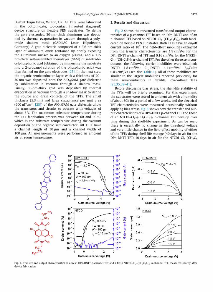
Fig. 2. Transfer and output characteristics of a fresh DPh-DNTT p-channel TFTdevice fabrication.
3. Results and discussion
Fig. 2 shows the measured transfer and output charac-teristics of a p-channel TFT based on DPh-DNTT and of ann-channel TFT based on NTCDI–Cl2–(CH2C3F7)2, both fabri-cated on flexible PEN substrates. Both TFTs have an on/offcurrent ratio of 107. The field-effect mobilities extractedfrom the transfer characteristics are 1.9 cm2/Vs for theDPh-DNTT p-channel TFT and 0.16 cm2/Vs for the NTCDI–Cl2–(CH2C3F7)2 n-channel TFT. For the other three semicon-ductors, the following carrier mobilities were obtained:DNTT: 1.8 cm2/Vs; C10-DNTT: 4.1 cm2/Vs; F16CuPc:0.03 cm2/Vs (see also Table 1). All of these mobilities aresimilar to the largest mobilities reported previously forthese semiconductors in flexible, low-voltage TFTs[25,35,38–41].
Before discussing bias stress, the shelf-life stability ofthe TFTs will be briefly examined. For this experiment,the substrates were stored in ambient air with a humidityof about 50% for a period of a few weeks, and the electricalTFT characteristics were measured occasionally withoutapplying bias stress. Fig. 3 shows how the transfer and out-put characteristics of a DPh-DNTT p-channel TFT and thoseof an NTCDI–Cl2–(CH2C3F7)2 n-channel TFT develop overtime during this shelf-life experiment. As can be seen,there is essentially no change in the threshold voltageand very little change in the field-effect mobility of eitherof the TFTs during shelf-life storage (40 days in air for theDPh-DNTT TFT; 10 days in air for the NTCDI–Cl2–(CH2C3
and a fresh NTCDI–Cl2–(CH2C3F7)2 n-channel TFT, measured shortly after

Table 1Measured field-effect mobilities, on/off current ratios, subthreshold swings and threshold voltages of flexible TFTs based on the five organic semiconductorsinvestigated in this study.
Semiconductor DNTT C10-DNTT DPh-DNTT F16CuPc NTCDI–Cl2–(CH2C3F7)2
Carrier type p-Channel TFT p-Channel TFT p-Channel TFT n-Channel TFT n-Channel TFT
Process temperature 60 �C 80 �C 80 �C 90 �C 65 �CField-effect mobility 1.8 cm2/Vs 4.1 cm2/Vs 1.9 cm2/Vs 0.03 cm2/Vs 0.16 cm2/VsOn/off current ratio 106 108 107 106 107
Subthreshold swing 100 mV/dec 200 mV/dec 180 mV/dec 360 mV/dec 110 mV/decThreshold voltage �1.2 V 0.4 V �0.8 V 0.1 V 0.2 V
Fig. 3. Shelf-life stability (without applying any bias stress) of DPh-DNTT p-channel and NTCDI–Cl2–(CH2C3F7)2 n-channel TFTs.
3176 S. Bisoyi et al. / Organic Electronics 15 (2014) 3173–3182
F7)2 TFT). Shelf-life tests over longer periods have been thesubject of several previous reports [25,34,36,38,39].
During continuous application of constant gate-sourceand drain-source voltages (negative voltages in the caseof p-channel TFTs, positive voltages in the case of n-chan-nel TFTs), the on-state drain current can be expected todecay over time, due to the trapping of charges from thegate-induced carrier channel into localized states. A usefulbasis for meaningful comparisons of the stability againstthis bias-stress-induced current decay among TFTs basedon different materials and/or different technologies is the10%-current-decay lifetime, which according to Hekmats-hoar et al. [42] is defined as the time until the drain currenthas dropped to 90% of its initial value. Hekmatshoar et al.also demonstrated the large extent to which the 10%-life-time depends on the applied gate-source voltage, makingit necessary to measure it for a range of applied voltagesin order to facilitate useful benchmarking [42]. For hydro-genated amorphous silicon (a-Si:H) n-channel TFTs fabri-cated at substrate temperatures ranging from 200 �C to
350 �C and stressed with gate-source voltages rangingfrom 7.5 V to 120 V, Hekmatshoar et al. determined 10%-lifetimes ranging from less than a minute (lowest processtemperature, largest gate bias) to more than a decade(highest process temperature, smallest gate bias) [27,42].
Fig. 4 shows how the drain current of flexible organicp-channel and n-channel TFTs based on DPh-DNTT andNTCDI–Cl2–(CH2C3F7)2 develops over time during biasstress with applied gate-source and drain-source voltagesranging from ±2 V to ±3 V (corresponding to gate fieldsranging from 3.8 to 5.5 MV/cm). This is a useful range ofgate-source voltages for the TFTs employed in this study,since gate-source voltages below ±2 V will be too close tothe threshold voltage for some of the semiconductors,while gate-source voltages above ±3 V might damage thegate dielectric when applied over extended periods of time.The drain-source voltage was either set to be equal to theapplied gate-source voltage (VGS = VDS) or was set to ±3 V;this corresponds to a range of biasing conditions that isrepresentative for those under which the drive TFTs in

Fig. 4. Development of the drain current of p-channel TFTs based on DPh-DNTT, DNTT and C10-DNTT and of n-channel TFTs based on NTCDI–Cl2–(CH2C3F7)2
and F16CuPc during continuous bias stress with gate-source and drain-source voltages ranging from ±2 to ±3 V over periods of up to six days.
S. Bisoyi et al. / Organic Electronics 15 (2014) 3173–3182 3177
AMOLED display pixels operate most of the time. Identicalmeasurements were carried out on TFTs based on all fivesemiconductors, and the results for one set of applied volt-ages are shown in Fig. 4. Note that each bias-stress mea-surement was conducted on a fresh (i.e., not previouslystressed) transistor.
From these measurements, the 10%-current-decay life-times were extracted. The results are summarized inTable 2. Depending on the choice of the semiconductorand on the voltages applied during bias stress, the 10%-lifetimes of the flexible DNTT, C10-DNTT, DPh-DNTT,F16CuPc and NTCDI–Cl2–(CH2C3F7)2 TFTs range from 15 sto about 1 week. In Fig. 5a, the 10%-lifetimes of all TFTsare plotted as a function of the applied gate-source volt-age, once for the measurements in which the applieddrain-source voltage was identical to the applied gate-source voltage (VGS = VDS) and once for the measurements
Table 210%-Current-decay lifetimes measured during bias stress under five different binvestigated in this study.
Abs (VGS) duringbias stress (V)
Abs (VDS) duringbias stress (V)
DNTT p-channel TFT(s)
C10-DNTT p-channel TFT (s
2.0 2.0 364,000 40,0002.5 2.5 209,000 13,0003.0 3.0 27,000 20,0002.0 3.0 417,000 32,0002.5 3.0 58,000 20,000
in which the applied drain-source voltage was set to±3.0 V. The results confirm that a larger applied gate-source voltage generally leads to a shorter 10%-lifetimeand vice versa, as was previously reported by Hekmats-hoar et al. [42] and others [9,21,22]. In principle, theresults also allow conclusions regarding the bias-stressstability of organic TFTs depending on the choice of thesemiconductor. However, it should be kept in mind thatsince the TFTs have different threshold voltages depend-ing on the choice of the semiconductor (see Table 1),the same applied gate-source voltage will induce a differ-ent density of charge carriers in each TFT, which in turnmay result in a different trap rate during bias stress. Toaccount for this, the 10%-lifetimes are plotted in Fig. 5bas a function of the difference between the appliedgate-source voltage and the threshold voltage (gate over-drive voltage VGS–Vth). As can be seen, for the p-channel
ias conditions on flexible TFTs based on the five organic semiconductors
)DPh-DNTT p-channel TFT (s)
F16CuPc n-channel TFT (s)
NTCDI–Cl2–(CH2C3F7)2 n-channel TFT (s)
502,000 290 7300302,000 55 7300115,000 15 550145,000 480 251,000132,000 185 4800

Fig. 5. Dependence of the measured 10%-current-decay lifetimes of DNTT, C10-DNTT and DPh-DNTT p-channel and NTCDI–Cl2–(CH2C3F7)2 and F16CuPc n-channel TFTs on the gate-source and drain-source voltages applied during bias stress. (a) The 10%-decay lifetimes are plotted as a function of the appliedgate-source voltage. (b) The 10%-decay lifetimes are plotted as a function of the gate overdrive voltage, which is the difference between the applied gate-source voltage and the threshold voltage of the TFT.
3178 S. Bisoyi et al. / Organic Electronics 15 (2014) 3173–3182
TFTs, DPh-DNTT and C10-DNTT provide somewhat betterstability than DNTT. For the n-channel TFTs, the resultsshow that in addition to a substantially larger electronmobility, NTCDI–Cl2–(CH2C3F7)2 also provides signifi-cantly better bias-stress stability over the entire rangeof gate-source and drain-source voltages compared withF16CuPc. In general, the p-channel TFTs examined in thisstudy all provide larger carrier mobilities and betterbias-stress stability compared with the n-channel TFTs.
Fig. 6. Measured transfer and output characteristics of DPh-DNTT and DNTT p-cafter bias stress.
Closer examination of Fig. 4 shows that the drain cur-rent does not decay monotonically over time during biasstress. Especially for small applied gate-source voltages,i.e., when the bias-stress effect is relatively small, the draincurrent actually increases during the first few hours of biasstress. This is believed to be due to an initial time-depen-dent decrease of the contact resistance that has been pre-viously reported to occur in pentacene TFTs [43,44] andthat has been confirmed to also occur in TFTs based on at
hannel and NTCDI–Cl2–(CH2C3F7)2 and F16CuPc n-channel TFTs before and

S. Bisoyi et al. / Organic Electronics 15 (2014) 3173–3182 3179
least some of the organic semiconductors employed in thepresent study [45], although the exact physical or chemicalmechanism(s) responsible for this time-dependentdecrease of the contact resistance are not yet clear.
Concurrent with the observed bias-stress-induceddecay of the on-state drain current, the threshold voltageof the TFTs will shift in the direction of the gate-sourcevoltage applied during bias stress, i.e., towards more nega-tive threshold voltages in the case of p-channel TFTs andtowards more positive threshold voltages in the case ofn-channel TFTs. Fig. 6 shows the extent of this bias-stress-induced threshold voltage shift produced by oneparticular bias-stress condition (VGS = VDS = ±2 V). For theseexperiments, the transfer characteristics were measuredonce before bias stress and again immediately after (withina few seconds of) completion of the bias-stress experiment.The smallest threshold-voltage shifts are seen for the DPh-DNTT p-channel TFTs (DVth = �0.2 V after 138 h of biasstress) and for the NTCDI–Cl2–(CH2C3F7)2 n-channel TFTs(DVth � 0 V after 64 h of bias stress), which is in line withthe trends seen in the 10%-current-decay lifetimes summa-rized in Table 2 and Fig. 5.
A comparison of the transfer characteristics recordedbefore and after long-term bias stress further reveals thatfor some of the semiconductors investigated in this study,the carrier mobility decreases during bias stress. For exam-ple, the carrier mobility of the DNTT TFTs drops from1.8 cm2/Vs before bias stress to 1.0 cm2/Vs after 110 h ofbias stress. Note that this is not the intrinsic mobility ofthe semiconductor channel, but an effective (apparent)
Fig. 7. Transfer and output characteristics of DPh-DNTT p-channel and NTCDI–Crelaxation of the transistors, showing the complete recovery of the original curr
mobility that is extracted from the transfer characteristicsand is smaller than the intrinsic channel mobility due tothe influence of extrinsic factors, most importantly dueto the contact resistance [46]. For pentacene TFTs, Wanget al. have reported an increase of the contact resistanceduring bias stress [47,48], which would cause the effectivemobility to decrease, even if the intrinsic mobility was notaffected by the bias stress. Thus, it is reasonable to hypoth-esize that the bias-stress-induced decrease of the effectivemobility seen in Fig. 6 is due to an increase in the contactresistance, rather than to a decrease of the intrinsic chan-nel mobility. To test this hypothesis it is useful to monitorthe relaxation of the transistors after bias stress. The rea-son is that in organic TFTs, the bias-stress-induced changesare usually not permanent, i.e., after the applied voltagesare reduced or removed, at least some of the trappedcharge carriers are released, the threshold voltage shiftsback towards its initial value, and the original current–voltage characteristics are at least partially recovered. InFig. 7 this is shown for the DPh-DNTT p-channel TFTsand the NTCDI–Cl2–(CH2C3F7)2 n-channel TFTs. For bothTFTs, an almost complete recovery of the original cur-rent–voltage characteristics is observed after a period 1or 2 days of relaxation with the transistor terminals float-ing. In those TFTs in which the bias stress had produceda notable drop in the effective mobility (especially in theDNTT TFTs), a partial recovery of the effective mobilitywas observed (see Table 3).
To benchmark the 10%-current-decay lifetimes ofTFTs fabricated using different materials or different
l2–(CH2C3F7)2 n-channel TFTs before bias stress, after bias stress and afterent–voltage characteristics after relaxation.

Table 3Changes in the effective field-effect mobility and the threshold voltage of the TFTs during and after bias stress.
Semiconductor DNTT C10-DNTT DPh-DNTT F16CuPc NTCDI–Cl2–(CH2C3F7)2
Carrier type p-Channel TFT p-Channel TFT p-Channel TFT n-Channel TFT n-Channel TFT
VGS during bias stress �2.0 V �2.0 V �2.0 V 2.0 V 2.0 VVDS during bias stress �2.0 V �2.0 V �2.0 V 3.0 V 3.0 VDuration of bias stress 398,000 s 44,000 s 661,000 s 16,000 s 252,000 sEffective mobility before bias stress 1.8 cm2/Vs 4.1 cm2/Vs 1.8 cm2/Vs 0.03 cm2/Vs 0.16 cm2/VsEffective mobility after bias stress 1.0 cm2/Vs 2.4 cm2/Vs 1.8 cm2/Vs 0.01 cm2/Vs 0.13 cm2/VsEffective mobility after recovery 1.6 cm2/Vs n/a 1.8 cm2/Vs 0.02 cm2/Vs 0.12 cm2/VsThreshold voltage before bias stress �1.2 V 0.4 V �0.8 V 0.1 V 0.2 VThreshold voltage after bias stress �1.7 V 0.1 V �1.1 V 0.9 V 0.3 VThreshold voltage after recovery �1.2 V n/a �0.8 V 0.8 V 0.2 V
Fig. 8. Comparison of the bias-stress stability of TFTs fabricated invarious technologies (a-Si:H, metal oxides, organic TFTs) on the basis ofthe 10%-current-decay lifetime plotted versus the channel sheet resis-tance. The a-Si:H data were taken from Ref. [42], the metal-oxide TFT datawere taken from Refs. [49–51] and the organic-TFT data were taken fromTable 2.
3180 S. Bisoyi et al. / Organic Electronics 15 (2014) 3173–3182
technologies, Hekmatshoar et al. [42] suggested to plot the10%-lifetimes against the transistor’s channel sheet resis-tance, which is inversely proportional to the field-effectmobility, the gate-dielectric capacitance per unit area andthe applied gate-source voltage. Fig. 8 summarizes someof the data reported by Hekmatshoar et al. [42] and others[49–51] for a-Si:H and metal-oxide TFTs fabricated at var-ious process temperatures ranging from 150 to 350 �C and,for comparison, the data obtained in this study for DPh-DNTT p-channel and NTCDI–Cl2–(CH2C3F7)2 n-channelTFTs fabricated at process temperatures below 100 �C.For each data point, the channel sheet resistance wasextracted from the output characteristics (drain currentvs. drain-source voltage) measured before bias stress atthe same gate-source voltage applied during the bias-stress experiment. From the data reported for a-Si:H andmetal-oxide TFTs, two trends emerge. One is that for thesame TFT, the 10%-lifetime is shorter when the channelsheet resistance is smaller, i.e., when the gate-source volt-age applied during bias stress is larger. This trend has beenwell documented [9,21–23,27,42] and is likely related tothe fact that the gate-induced carrier density and hencethe trapping rate increase with increasing gate-sourcevoltage. The second trend is that inorganic TFTs fabricatedat higher process temperatures have longer 10%-lifetimesthan inorganic TFTs fabricated at lower process tempera-tures [42], which is likely related to the fact that in the
fabrication of inorganic TFTs, higher process temperaturesgenerally produce films and interfaces with smaller defectdensities. However, process temperatures above about200 �C make it difficult to fabricate the TFTs on flexibleplastic substrates, which often have glass transition tem-peratures below about 200 �C. (Plastics with higher glasstransition temperatures exist, but they tend to be moreexpensive than polyethylene naphthalate and polyethyl-ene terephthalate, which have glass transition tempera-tures below 150 �C.) Fig. 8 shows that the bias-stressstability of at least some of the organic p-channel TFTsinvestigated in this study is actually better than that ofmany inorganic TFTs, despite the fact that the organic TFTswere fabricated at much lower process temperatures onpolyethylene naphthalate substrates. But Fig. 8 also showsthat more work is needed to further improve the bias-stress stability of flexible organic n-channel TFTs.
4. Conclusions
In conclusion, the bias-stress stability of flexible p-channel and n-channel transistors based on five promisingorganic semiconductors was investigated and comparedwith that of several inorganic TFTs reported in literature.Particular emphasis was put on quantifying the extent towhich the bias-stress-induced decay of the on-state draincurrent of the TFTs is affected by the choice of the semicon-ductor and by the applied gate-source and drain-sourcevoltages. For TFTs based on at least some of the semicon-ductors investigated in this study, especially 2,9-diphenyl-dinaphtho[2,3-b:20,30-f]thieno[3,2-b]thiophene (DPh-DNTT),the bias-stress stability is already comparable to that ofa-Si:H and metal-oxide TFTs, despite the fact that theorganic TFTs were fabricated at significantly lower processtemperatures, which is important in view of the fabricationof these devices on plastic substrates.
Acknowledgements
This work was partially funded by BASF SE and by theGerman Ministry of Education and Research (BMBF) underGrants 13N10205, 13N12084 and 13N10763 (POLYTOSand KOSADIS; Research Network Forum Organic Electron-ics) and under Grant 1612000463 (KoSiF). The authorsgratefully acknowledge BASF SE, Ludwigshafen, Germany,for providing the organic semiconductor NTCDI–Cl2–(CH2

S. Bisoyi et al. / Organic Electronics 15 (2014) 3173–3182 3181
C3F7)2 employed in this study. Sibani Bisoyi would like tothank Klaus von Klitzing for providing the opportunity towork at the Max Planck Institute for Solid State Research.
References
[1] L. Zhou, A. Wanga, S.C. Wu, J. Sun, S. Park, T.N. Jackson, All-organicactive matrix flexible display, Appl. Phys. Lett. 88 (2006) 083502.
[2] I. Yagi, N. Hirai, Y. Miyamoto, M. Noda, A. Imaoka, N. Yoneya, K.Nomoto, J. Kasahara, A. Yumoto, T. Urabe, A flexible full-colorAMOLED display driven by OTFTs, J. Soc. Inf. Display 16 (2008) 15.
[3] Y. Nakajima, T. Takei, T. Tsuzuki, M. Suzuki, H. Fukagawa, T.Yamamoto, S. Tokito, Fabrication of 5.8-in. OTFT-driven flexiblecolor AMOLED display using dual protection scheme for organicsemiconductor patterning, J. Soc. Inf. Display 17 (2009) 629.
[4] M. Noda, N. Kobayashi, M. Katsuhara, A. Yumoto, S. Ushikura, R.Yasuda, N. Hirai, G. Yukawa, I. Yagi, K. Nomoto, T. Urabe, An OTFT-driven rollable OLED display, J. Soc. Inf. Display 19 (2011) 316.
[5] Y. Fujisaki, Y. Nakajima, T. Takei, H. Fukagawa, T. Yamamoto, H.Fujikake, Flexible active-matrix organic light-emitting diode displayusing air-stable organic semiconductor of dinaphtho[2,3-b:20 ,30-f]thieno[3,2-b]-thiophene, IEEE Trans. Electr. Dev. 59 (2012) 3442.
[6] S. Steudel, K. Myny, S. Schols, P. Vicca, S. Smout, A. Tripathi, B. vander Putten, J.L. van der Steen, M. van Neer, F. Schütze, O.R. Hild, E.van Veenendaal, P. van Lieshout, M. van Mil, J. Genoe, G. Gelinck, P.Heremans, Design and realization of a flexible QQVGA AMOLEDdisplay with organic TFTs, Org. Electron. 13 (2012) 1729.
[7] R. Meerheim, S. Olthof, M. Hermenau, S. Scholz, A. Petrich, N. Tessler,O. Solomeshch, B. Lüssem, M. Riede, K. Leo, Investigation of C60F36 aslow-volatility p-dopant in organic optoelectronic devices, J. Appl.Phys. Lett. 109 (2011) 103102.
[8] A. Salleo, R.A. Street, Light-induced bias stress reversal inpolyfluorene thin-film transistors, J. Appl. Phys. 94 (2003) 471.
[9] R.A. Street, M. Chabinyc, F. Endicott, B. Ong, Extended time biasstress effects in polymer transistors, J. Appl. Phys. 100 (2006)114518.
[10] H. Sirringhaus, Reliability of organic field-effect transistors, Adv.Mater. 21 (2009) 3859.
[11] P.A. Bobbert, A. Sharma, S.G.J. Mathijssen, M. Kemerink, D.M. deLeeuw, Operational stability of organic field-effect transistors, Adv.Mater. 24 (2012) 1146.
[12] T. Richards, H. Sirringhaus, Bias-stress induced contact and channeldegradation in staggered and coplanar organic field-effecttransistors, Appl. Phys. Lett. 92 (2008) 023512.
[13] W.L. Kalb, T. Mathis, S. Haas, A.F. Stassen, B. Batlogg, Organic smallmolecule field-effect transistors with CytopTM gate dielectric:eliminating gate bias stress effects, Appl. Phys. Lett. 90 (2007)092104.
[14] X.H. Zhang, S.P. Tiwari, B. Kippelen, Pentacene organic field-effecttransistors with polymeric dielectric interfaces: Performance andstability, Org. Electron. 10 (2009) 1133.
[15] F. Colleaux, J.M. Ball, P.H. Wöbkenberg, P.J. Hotchkiss, S.R. Marder,T.D. Anthopoulos, Bias-stress effects in organic field-effecttransistors based on self-assembled monolayer nanodielectrics,Phys. Chem. Chem. Phys. 13 (2011) 14387.
[16] J.H. Park, Y.T. Lee, H.S. Lee, J.Y. Lee, K. Lee, G.B. Lee, J. Han, T.W. Kim, S.Im, Origin of bias-stress induced instability in organic thin-filmtransistors with semiconducting small-molecule/insulating polymerblend channel, ACS Appl. Mater. Interfaces 5 (2013) 1625.
[17] R. Häusermann, B. Batlogg, Gate bias stress in pentacene field-effect-transistors: charge trapping in the dielectric or semiconductor, Appl.Phys. Lett. 99 (2011) 083303.
[18] S.P. Tiwari, X.H. Zhang, W.J. Potscavage, B. Kippelen, Study ofelectrical performance and stability of solution-processed n-channel organic field-effect transistors, J. Appl. Phys. 106 (2009)054504.
[19] T. Sekitani, S. Iba, Y. Kato, Y. Noguchi, T. Someya, T. Sakurai,Suppression of DC bias stress-induced degradation of organic field-effect transistors using postannealing effects, Appl. Phys. Lett. 87(2005) 073505.
[20] H.L. Gomes, P. Stallinga, M. Cölle, D.M. de Leeuw, F. Biscarini,Electrical instabilities in organic semiconductors caused by trappedsupercooled water, Appl. Phys. Lett. 88 (2006) 082101.
[21] H.W. Zan, S.C. Kao, The effects of drain-bias on the threshold voltageinstability in organic TFTs, IEEE Electr. Dev. Lett. 29 (2008) 155.
[22] U. Zschieschang, R.T. Weitz, K. Kern, H. Klauk, Bias stress effect inlow-voltage organic thin-film transistors, Appl. Phys. A. 95 (2009) 139.
[23] S.P. Tiwari, X.H. Zhang, W.J. Potscavage Jr., B. Kippelen, Low-voltagesolution-processed n-channel organic field-effect transistors withhigh-k HfO2 gate dielectrics grown by atomic layer deposition, Appl.Phys. Lett. 95 (2009) 223303.
[24] D.K. Hwang, C. Fuentes-Hernandez, J.B. Kim, W.J. Potscavage Jr., B.Kippelen, Flexible and stable solution-processed organic field-effecttransistors, Org. Electron. 12 (2011) 1108.
[25] U. Zschieschang, M.J. Kang, K. Takimiya, T. Sekitani, T. Someya, T.W.Canzler, A. Werner, J. Blochwitz-Nimoth, H. Klauk, Flexible low-voltage organic thin-film transistors and circuits based on C10-DNTT,J. Mater. Chem. 22 (2012) 4273.
[26] K. Suemori, M. Taniguchi, T. Kamata, Effect of silicon dioxide surfaceon bias stress effect for organic field-effect transistors, Jpn. J. Appl.Phys. 48 (2009) 04C170.
[27] B. Hekmatshoar, K.H. Cherenack, A.Z. Kattamis, K. Long, S. Wagner,J.C. Sturm, Highly stable amorphous-silicon thin-film transistors onclear plastic, Appl. Phys. Lett. 93 (2008) 032103.
[28] T. Zaki, S. Scheinert, I. Hörselmann, R. Rödel, F. Letzkus, H. Richter, U.Zschieschang, H. Klauk, J.N. Burghartz, Accurate capacitancemodeling and characterization of organic thin-film transistors, IEEETrans. Electr. Dev. 61 (2014) 98.
[29] T. Yamamoto, K. Takimiya, Facile synthesis of highly-extendedheteroarenes, dinaphtho[2,3-b:20 ,30-f]chalcogenopheno[3,2-b]chalcogenophenes, and their application to field-effecttransistors, J. Am. Chem. Soc. 129 (2007) 2224.
[30] M.J. Kang, I. Doi, H. Mori, E. Miyazaki, K. Takimiya, M. Ikeda, H.Kuwabara, Alkylated dinaphtho[2,3-b:20 ,30-f]thieno[3,2-b]thiophenes (Cn-DNTTs): organic semiconductors for high-performance thin-film transistors, Adv. Mater. 23 (2011) 1222.
[31] K. Niimi, M.J. Kang, E. Miyazaki, I. Osaka, K. Takimiya, Generalsynthesis of dinaphtho-[2,3-b:2030-f]thieno[3,2-b]thiophene (DNTT)derivatives, Org. Lett. 13 (2011) 3430.
[32] Z. Bao, A. Lovinger, J. Brown, New air-stable n-channel organic thinfilm transistors, J. Am. Chem. Soc. 120 (1998) 207.
[33] J.H. Oh, S.L. Suraru, W.Y. Lee, M. Könemann, H.W. Höffken, C. Röger,R. Schmidt, Y. Chung, W.C. Chen, F. Würthner, Z. Bao, High-performance air-stable n-type organic transistors based on core-chlorinated naphthalene tetracarboxylic diimides, Adv. Funct. Mater.20 (2010) 2148.
[34] E.D. Glowacki, M. Irimia-Vladu, M. Kaltenbrunner, J. Gasiorowski,M.S. White, U. Monkowius, G. Romanazzi, G.P. Suranna, P.Mastrorilli, T. Sekitani, S. Bauer, T. Someya, L. Torsi, N.S. Sariciftci,Hydrogen-bonded semiconducting pigments for air-stable field-effect transistors, Adv. Mater. 25 (2013) 1563.
[35] T. Yokota, K. Kuribara, T. Tokuhara, U. Zschieschang, H. Klauk, K.Takimiya, Y. Sadamitsu, M. Hamada, T. Sekitani, T. Someya, Flexiblelow-voltage organic transistors with high thermal stability at 250 �C,Adv. Mater. 25 (2013) 3639.
[36] M.M. Ling, Z. Bao, Copper hexafluorophthalocyanine field-effecttransistors with enhanced mobility by soft contact lamination, Org.Electron. 7 (2006) 568.
[37] M. Stolte, M. Gsänger, R. Hofmockel, S.L. Suraru, F. Würthner,Improved ambient operation of n-channel organic transistors ofsolution-sheared naphthalene diimide under bias stress, Phys.Chem. Chem. Phys. 14 (2012) 14181.
[38] U. Zschieschang, F. Ante, D. Kälblein, T. Yamamoto, K. Takimiya, H.Kuwabara, M. Ikeda, T. Sekitani, T. Someya, J. Blochwitz-Nimoth, H.Klauk, Dinaphtho[2,3-b:20 ,30-f]thieno[3,2-b]thiophene (DNTT) thin-film transistors with improved performance and stability, Org.Electron. 12 (2011) 1370.
[39] R. Rödel, F. Letzkus, T. Zaki, J.N. Burghartz, U. Kraft, U. Zschieschang,K. Kern, H. Klauk, Contact properties of high-mobility, air-stable,low-voltage organic n-channel thin-film transistors based on anaphthalene tetracarboxylic diimide, Appl. Phys. Lett. 102 (2013)233303.
[40] K. Ishida, N. Masunaga, R. Takahashi, T. Sekitani, S. Shino, U.Zschieschang, H. Klauk, M. Takamiya, T. Someya, T. Sakurai, Usercustomizable logic paper (UCLP) with sea-of transmission-gates(SOTG) of 2-V organic CMOS and ink-jet printed interconnects, IEEEJ. Solid-State Circ. 46 (2011) 285.
[41] I. Doi, M.J. Kang, K. Takimiya, High mobility organic thin-filmtransistors on plastic substrate, Curr. Appl. Phys. 12 (2012) e2.
[42] B. Hekmatshoar, S. Wagner, J.C. Sturm, Tradeoff regimes of lifetimein amorphous silicon thin-film transistors and a universallifetime comparison framework, Appl. Phys. Lett. 95 (2009)143504.
[43] W.L. Kalb, F. Meier, K. Mattenberger, B. Batlogg, Defect healing atroom temperature in pentacene thin films and improved transistorperformance, Phys. Rev. B 76 (2007) 184112.

3182 S. Bisoyi et al. / Organic Electronics 15 (2014) 3173–3182
[44] X. Lu, T. Minari, A. Kumatani, C. Liu, K. Tsukagoshi, Effect of airexposure on metal/organic interface in organic field-effecttransistors, Appl. Phys. Lett. 98 (2011) 243301.
[45] U. Kraft, U. Zschieschang, K. Takimiya, E. Weber, H. Klauk, Time-Dependent Improvement in Contact Resistance and DynamicPerformance of Low-Voltage Organic p-Channel TFTs based on Air-Stable DNTT Derivatives, in: 56th Electronic Materials Conference,Santa Barbara, 2014. (manuscript in preparation).
[46] F. Ante, D. Kälblein, T. Zaki, U. Zschieschang, K. Takimiya, M. Ikeda, T.Sekitani, T. Someya, J.N. Burghartz, K. Kern, H. Klauk, Contactresistance and megahertz operation of aggressively scaled organictransistors, Small 8 (2012) 73.
[47] S.D. Wang, T. Minari, T. Miyadera, Y. Aoyagi, K. Tsukagoshi, Biasstress instability in pentacene thin-film transistors: contactresistance change and channel threshold voltage shift, Appl. Phys.Lett. 92 (2008) 063305.
[48] Y. Yan, X.J. She, H. Zhu, S.D. Wang, Origin of bias stress inducedinstability of contact resistance in organic thin film transistors, Org.Electron. 12 (2011) 823.
[49] T. Riedl, P. Görrn, P. Hölzer, W. Kowalsky, Ultra-high long-termstability of oxide-TTFTs under current stress, Phys. Stat. Sol. (RRL) 5(2007) 175.
[50] D.H. Levy, D. Freeman, S.F. Nelson, P.J. Cowdery-Corvan, L.M. Irving,Stable ZnO thin film transistors by fast open air atomic layerdeposition, Appl. Phys. Lett. 92 (2008) 192101.
[51] S. Yang, J.Y. Bak, S.M. Yoon, M.K. Ryu, H. Oh, C.S. Hwang, G.H. Kim,S.H.K. Park, J. Jang, Low-temperature processed flexible In–Ga–Zn–Othin-film transistors exhibiting high electrical performance, IEEEElect. Dev. Lett. 32 (2011) 1692.