Embed Size (px)
Citation preview
1
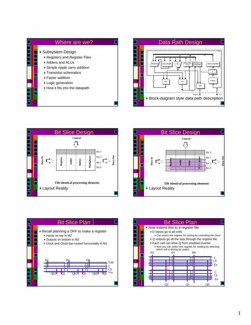
Where are we? Subsystem Design
Registers and Register FilesAdders and ALUsSimple ripple carry additionTransistor schematicsFaster additionLogic generationHow it fits into the datapath
Data Path Design
Block-diagram style data path description
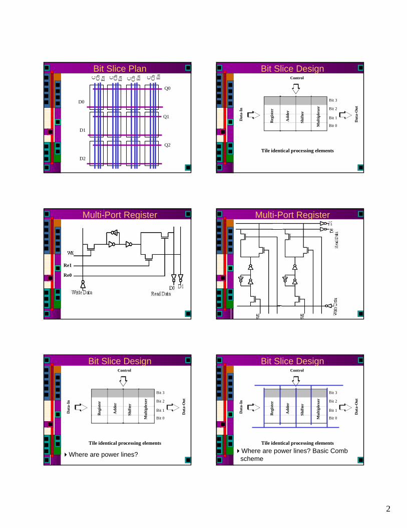
Bit Slice Design
Bit 3
Bit 2
Bit 1
Bit 0
Reg
ister
Add
er
Shift
er
Mul
tiple
xer
Control
Dat
a-In
Dat
a-O
ut
Tile identical processing elements
Layout Reality
Bit Slice Design
Bit 3
Bit 2
Bit 1
Bit 0R
egist
er
Add
er
Shift
er
Mul
tiple
xer
Control
Dat
a-In
Dat
a-O
ut
Tile identical processing elementsLayout Reality
Bit Slice PlanRecall planning a DFF to make a register
Inputs on top in M2Outputs on bottom in M2Clock and Clock-bar routed horizontally in M1
Vdd
CbC
Vss
D0
Q0Qb0
D1
Q1Qb1
D2
Q2Qb2
Bit Slice PlanNow extend this to a register file
D inputs go to all cellsCan select one register for writing by controlling the clock
Q outputs go all the way through the register fileEach cell can drive Q from enabled inverter
Now you can select one register for reading by selecting which cell is driving its output
CbC
D0
Q0
D1
Q1
D2
Q2
En
CbC
En
2
Bit Slice Plan
Q0
Q1
Q2
D0
D1
D2
CbC En CbC EnCbCCbC EnEn
Bit Slice Design
Bit 3
Bit 2
Bit 1
Bit 0
Reg
ister
Add
er
Shift
er
Mul
tiple
xer
Control
Dat
a-In
Dat
a-O
ut
Tile identical processing elements
Multi-Port Register
Re1
Re0
Multi-Port Register
Bit Slice Design
Where are power lines?
Bit 3
Bit 2
Bit 1
Bit 0
Reg
ister
Add
er
Shift
er
Mul
tiple
xer
Control
Dat
a-In
Dat
a-O
ut
Tile identical processing elements
Bit Slice Design
Where are power lines? Basic Comb scheme
Bit 3
Bit 2
Bit 1
Bit 0
Reg
ister
Add
er
Shift
er
Mul
tiple
xer
Control
Dat
a-In
Dat
a-O
ut
Tile identical processing elements
3
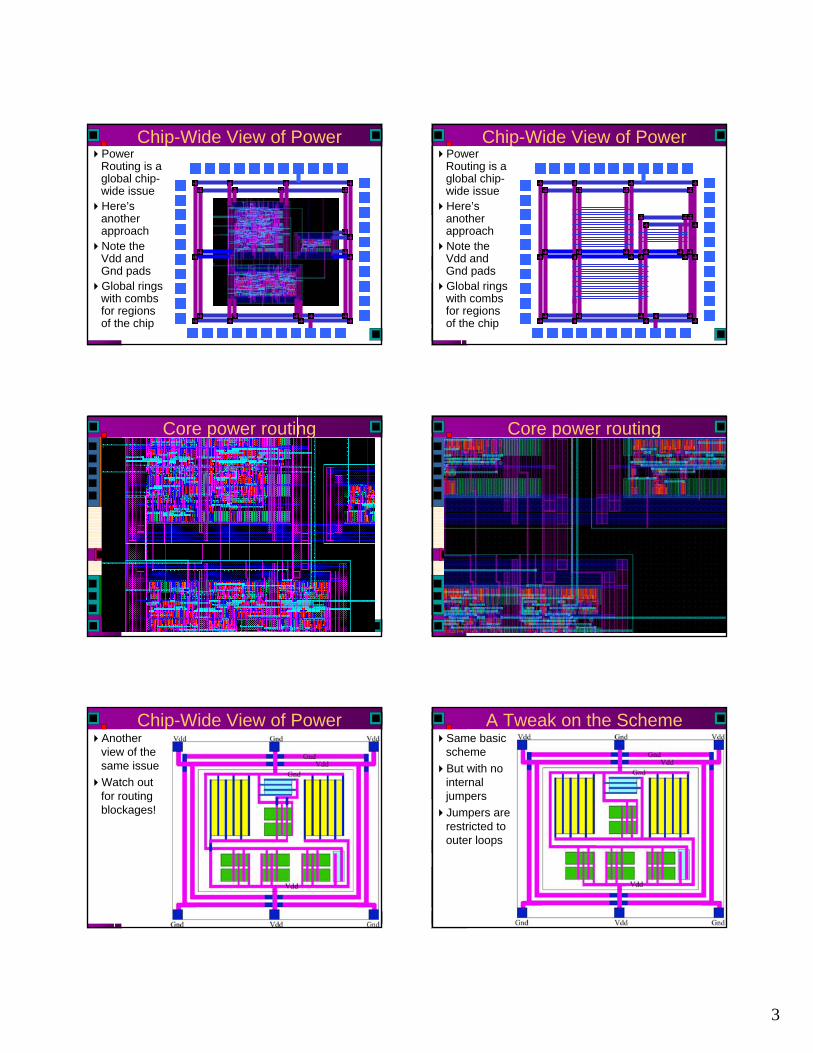
Chip-Wide View of PowerPower Routing is a global chip-wide issueHere’s another approachNote the Vdd and Gnd padsGlobal rings with combs for regions of the chip
Chip-Wide View of PowerPower Routing is a global chip-wide issueHere’s another approachNote the Vdd and Gnd padsGlobal rings with combs for regions of the chip
Core power routing Core power routing
Chip-Wide View of PowerAnother view of the same issueWatch out for routing blockages!
A Tweak on the SchemeSame basic schemeBut with no internal jumpersJumpers are restricted to outer loops
4
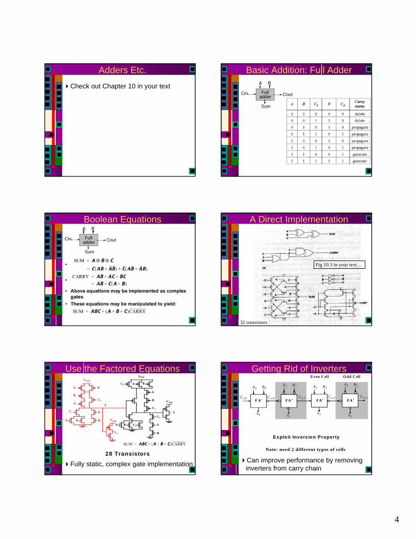
Adders Etc. Check out Chapter 10 in your text
Basic Addition: Full AdderA B
Cout
Sum
Cin Fulladder
Boolean EquationsA B
Cout
Sum
Cin Fulladder
A Direct Implementation
Fig 10.3 in your text…
32 transistors
Use the Factored Equations
Fully static, complex gate implementation
V DD
VD D
V DD
V D D
A B
C i
S
Co
X
B
A
C i A
BBA
C i
A B C i
C i
B
A
C i
A
B
BA
28 Transistors
Getting Rid of Inverters
Can improve performance by removing inverters from carry chain
A0 B0
S0
C o ,0Ci ,0
A1 B1
S1
Co ,1
A2 B2
S2
C o,2 C o ,3F A’ FA ’ FA’ FA ’
A3 B3
S3
O dd C ellEven C ell
Exploit Invers ion Property
Note: need 2 different typ es of cells
5
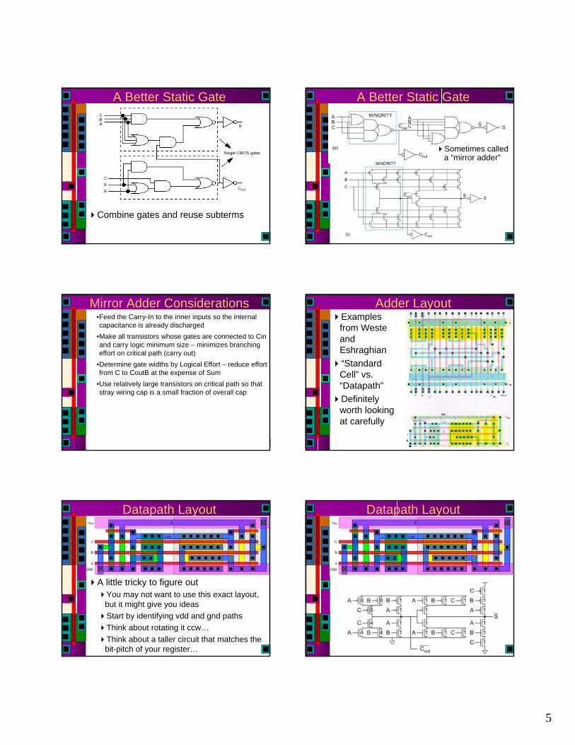
A Better Static Gate
Combine gates and reuse subterms
A Better Static Gate
Sometimes called a “mirror adder”
Mirror Adder Considerations•Feed the Carry-In to the inner inputs so the internal capacitance is already discharged
•Make all transistors whose gates are connected to Cin and carry logic minimum size – minimizes branching effort on critical path (carry out)
•Determine gate widths by Logical Effort – reduce effort from C to CoutB at the expense of Sum
•Use relatively large transistors on critical path so that stray wiring cap is a small fraction of overall cap
Adder LayoutExamples from Weste and Eshraghian“Standard Cell” vs. “Datapath”Definitely worth looking at carefully
Datapath Layout
A little tricky to figure outYou may not want to use this exact layout, but it might give you ideasStart by identifying vdd and gnd pathsThink about rotating it ccw… Think about a taller circuit that matches the bit-pitch of your register…
Datapath Layout
6
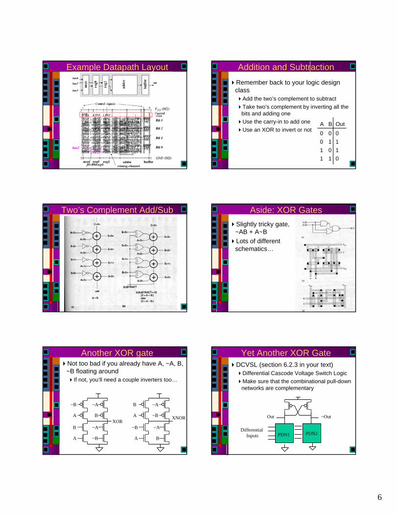
Example Datapath Layout Addition and SubtractionRemember back to your logic design class
Add the two’s complement to subtractTake two’s complement by inverting all the bits and adding oneUse the carry-in to add oneUse an XOR to invert or not
011101110000OutBA
Two’s Complement Add/Sub Aside: XOR GatesSlightly tricky gate, ~AB + A~BLots of different schematics…
Another XOR gateNot too bad if you already have A, ~A, B, ~B floating around
If not, you’ll need a couple inverters too…
A B
~A~B
A
B
~B
~AXOR
A B
~A~B
A
B
~B
~A
XNOR
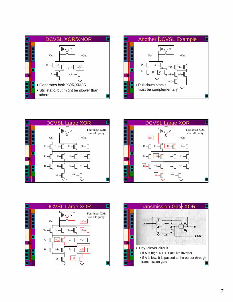
Yet Another XOR GateDCVSL (section 6.2.3 in your text)
Differential Cascode Voltage Switch LogicMake sure that the combinational pull-down networks are complementary
Differential Inputs PDN1 PDN2
Out ~Out
7
DCVSL XOR/XNOR
Generates both XOR/XNORStill static, but might be slower than others
Out ~Out
~A
~B
A
B~BB
Another DCVSL Example
Out ~Out
~A
~C
A
C~B
B
~ED
E~D
Pull-down stacksmust be complementary
DCVSL Large XOR
Out ~Out
~A
~C
A
C
~BB
D~D
~BB
~CC
D~D
Four-input XORaka odd parity
DCVSL Large XOR
Out ~Out
~A
~C
A
C
~BB
D~D
~BB
~CC
D~D
Four-input XORaka odd parity
DCVSL Large XOR
Out ~Out
~A
~C
A
C
~BB
D~D
~BB
~CC
D~D
Four-input XORaka odd parity
Transmission Gate XOR
Tiny, clever circuitIf A is high, N1, P1 act like inverterIf A is low, B is passed to the output through transmission gate
8
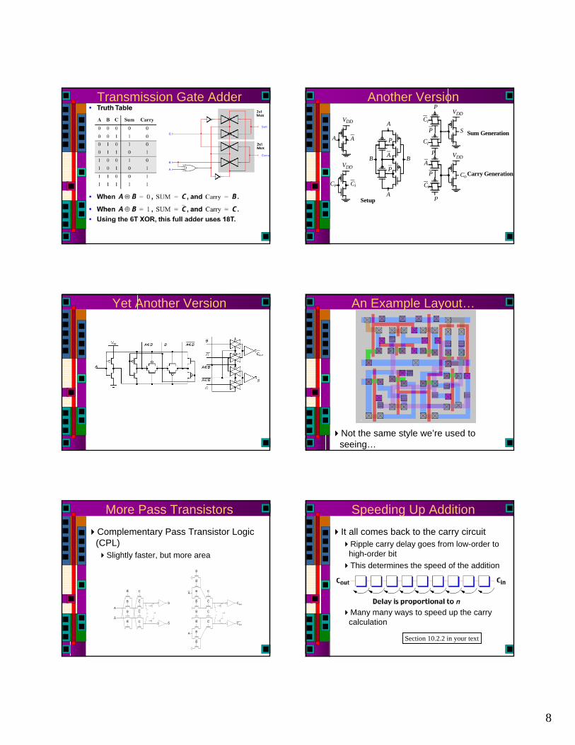
Transmission Gate Adder Another Version
A
B
P
Ci
VDDA
A A
VDD
Ci
A
P
AB
VDD
VDD
Ci
Ci
Co
S
Ci
P
P
P
P
P
Sum Generation
Carry Generation
Setup
Yet Another Version An Example Layout…
Not the same style we’re used to seeing…
More Pass TransistorsComplementary Pass Transistor Logic (CPL)
Slightly faster, but more area
A
C
S
S
B
B
C
C
C
B
B Cout
Cout
C
C
C
C
B
B
B
B
B
B
B
B
A
A
A
Speeding Up AdditionIt all comes back to the carry circuit
Ripple carry delay goes from low-order to high-order bitThis determines the speed of the addition
Many many ways to speed up the carry calculation
Section 10.2.2 in your text
9
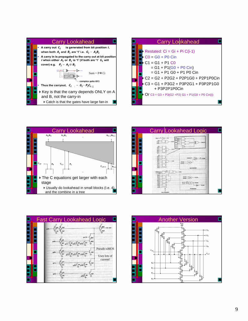
Carry Lookahead
Key is that the carry depends ONLY on A and B, not the carry-in
Catch is that the gates have large fan-in
Sum = P + Ci
-1
Carry LookaheadRestated: Ci = Gi + Pi C(i-1)C0 = G0 + P0 CinC1 = G1 + P1 C0
= G1 + P1(G0 + P0 Cin)= G1 + P1 G0 + P1 P0 Cin
C2 = G2 + P2G2 + P2P1G0 + P2P1P0CinC3 = G1 + P3G2 + P3P2G1 + P3P2P1G0
+ P3P2P1P0CinOr C3 = G3 + P3(G2 +P2( G1 + P1(G0 + P0 Cin)))
Carry Lookahead
The C equations get larger with each stage
Usually do lookahead in small blocks (I.e. 4) and the combine in a tree
A0,B0 A1,B1 AN -1,BN-1...
Ci,0 P0 Ci,1 P1Ci,N -1 PN -1
...
Carry Lookahead Logic
Fast Carry Lookahead Logic
Pseudo-nMOS
Uses lots ofcurrent!
Another Version VDD
P3
P2
P1
P0
G3
G2
G1
G0
Ci,0
Co,3
10
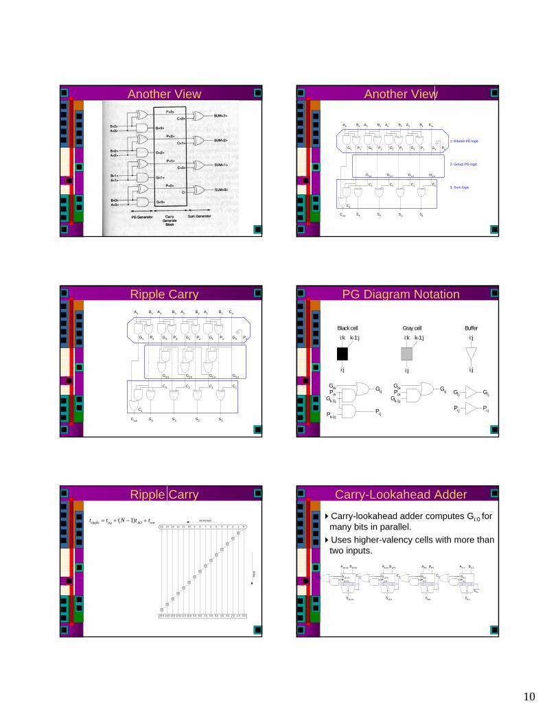
Another View Another View
S1
B1A1
P1G1
G0:0
S2
B2
P2G2
G1:0
A2
S3
B3A3
P3G3
G2:0
S4
B4
P4G4
G3:0
A4 Cin
G0 P0
1: Bitwise PG logic
2: Group PG logic
3: Sum logicC0C1C2C3
Cout
C4
Ripple Carry
S1
B1A1
P1G1
G0:0
S2
B2
P2G2
G1:0
A2
S3
B3A3
P3G3
G2:0
S4
B4
P4G4
G3:0
A4 Cin
G0 P0
C0C1C2C3
Cout
C4
PG Diagram Notation
i:j
i:j
i:k k-1:j
i:j
i:k k-1:j
i:j
Gi:k
Pk-1:j
Gk-1:j
Gi:j
Pi:j
Pi:k
Gi:k
Gk-1:j
Gi:j Gi:j
Pi:j
Gi:j
Pi:j
Pi:k
Black cell Gray cell Buffer
Ripple Carry
Delay
0123456789101112131415
15:0 14:0 13:0 12:0 11:0 10:0 9:0 8:0 7:0 6:0 5:0 4:0 3:0 2:0 1:0 0:0
Bit Positionripple xor( 1)pg AOt t N t t= + − +
Carry-Lookahead AdderCarry-lookahead adder computes Gi:0 for many bits in parallel.Uses higher-valency cells with more than two inputs.
Cin+
S4:1
G4:1P4:1
A4:1 B4:1
+
S8:5
G8:5P8:5
A8:5 B8:5
+
S12:9
G12:9P12:9
A12:9 B12:9
+
S16:13
G16:13P16:13
A16:13 B16:13
C4C8C12Cout
11
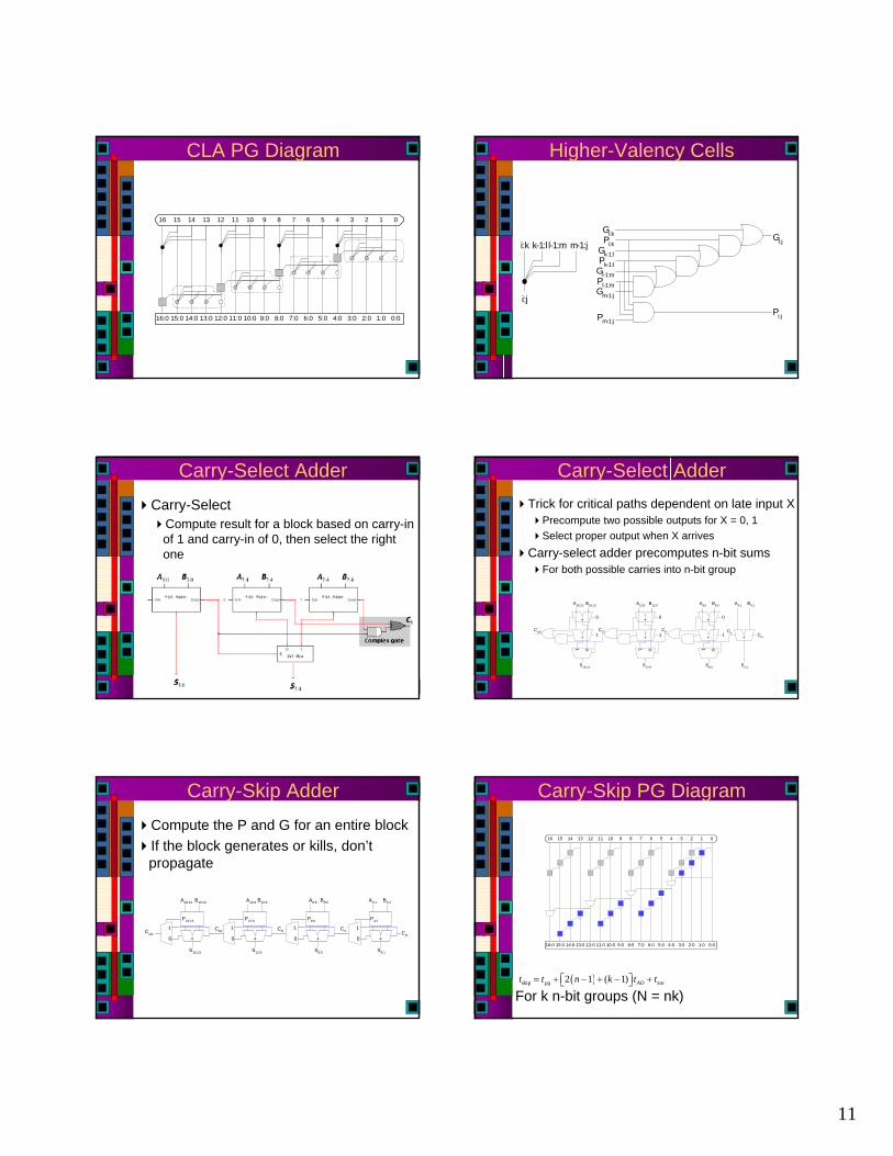
CLA PG Diagram
012345678910111213141516
15:0 14:0 13:0 12:0 11:0 10:0 9:0 8:0 7:0 6:0 5:0 4:0 3:0 2:0 1:0 0:016:0
Higher-Valency Cells
i:j
i:k k-1:l l-1:m m-1:j
Gi:k
Gk-1:l
Gl-1:m
Gm-1:j
Gi:j
Pi:j
Pi:k
Pk-1:l
Pl-1:m
Pm-1:j
Carry-Select AdderCarry-Select
Compute result for a block based on carry-in of 1 and carry-in of 0, then select the right one
Carry-Select AdderTrick for critical paths dependent on late input X
Precompute two possible outputs for X = 0, 1Select proper output when X arrives
Carry-select adder precomputes n-bit sumsFor both possible carries into n-bit group
Cin+
A4:1 B4:1
S4:1
C4
+
+
01
A8:5 B8:5
S8:5
C8
+
+
01
A12:9 B12:9
S12:9
C12
+
+
01
A16:13 B16:13
S16:13
Cout
0
1
0
1
0
1
Carry-Skip AdderCompute the P and G for an entire blockIf the block generates or kills, don’t propagate
Cin+
S4:1
P4:1
A4:1 B4:1
+
S8:5
P8:5
A8:5 B8:5
+
S12:9
P12:9
A12:9 B12:9
+
S16:13
P16:13
A16:13 B16:13
CoutC4
1
0
C81
0
C121
0
1
0
Carry-Skip PG Diagram
For k n-bit groups (N = nk)( )skip xor2 1 ( 1)pg AOt t n k t t= + − + − +⎡ ⎤⎣ ⎦
012345678910111213141516
15:0 14:0 13:0 12:0 11:0 10:0 9:0 8:0 7:0 6:0 5:0 4:0 3:0 2:0 1:0 0:016:0
12
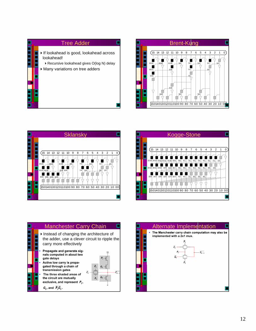
Tree AdderIf lookahead is good, lookahead across lookahead!
Recursive lookahead gives O(log N) delayMany variations on tree adders
Brent-Kung
1:03:25:47:69:811:1013:1215:14
3:07:411:815:12
7:015:8
11:0
5:09:013:0
0123456789101112131415
15:014:013:012:011:010:0 9:0 8:0 7:0 6:0 5:0 4:0 3:0 2:0 1:0 0:0
Sklansky
1:0
2:03:0
3:25:47:69:811:1013:1215:14
6:47:410:811:814:1215:12
12:813:814:815:8
0123456789101112131415
15:014:013:012:011:010:0 9:0 8:0 7:0 6:0 5:0 4:0 3:0 2:0 1:0 0:0
Kogge-Stone
1:02:13:24:35:46:57:68:79:810:911:1012:1113:1214:1315:14
3:04:15:26:37:48:59:610:711:812:913:1014:1115:12
4:05:06:07:08:19:210:311:412:513:614:715:8
2:0
0123456789101112131415
15:014:013:012:011:010:0 9:0 8:0 7:0 6:0 5:0 4:0 3:0 2:0 1:0 0:0
Manchester Carry ChainInstead of changing the architecture of the adder, use a clever circuit to ripple the carry more effectively
Alternate Implementation
13
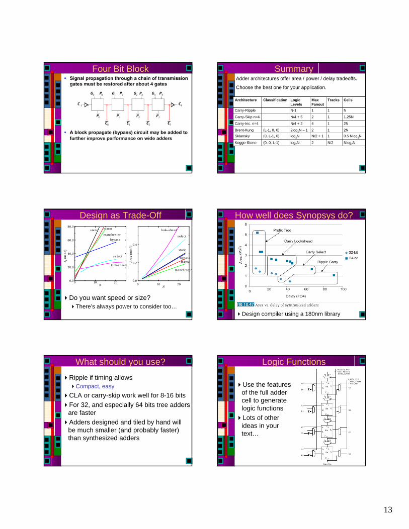
Four Bit Block SummaryAdder architectures offer area / power / delay tradeoffs.
Choose the best one for your application.
Nlog2NN/22log2N(0, 0, L-1)Kogge-Stone
0.5 Nlog2N1N/2 + 1log2N(0, L-1, 0)Sklansky2N122log2N – 1(L-1, 0, 0)Brent-Kung
2N14N/4 + 2Carry-Inc. n=4
1.25N12N/4 + 5Carry-Skip n=4
N11N-1Carry-Ripple
CellsTracksMax Fanout
Logic Levels
ClassificationArchitecture
Design as Trade-Off
Do you want speed or size? There’s always power to consider too…
0 10 20N
0.0
20.0
40.0
60.0
80.0
t p (n
sec)
0 10 20N
0.0
0.2
0.4
Are
a (m
m2)
look-ahead
se lect
bypassmanches te r
mirrors ta tic
manches te r
look-ahead
se lect
s tatic
mirrorbypass
How well does Synopsys do?
Design compiler using a 180nm library
What should you use? Ripple if timing allows
Compact, easyCLA or carry-skip work well for 8-16 bitsFor 32, and especially 64 bits tree adders are fasterAdders designed and tiled by hand will be much smaller (and probably faster) than synthesized adders
Logic Functions
Use the features of the full adder cell to generate logic functionsLots of other ideas in your text…
14
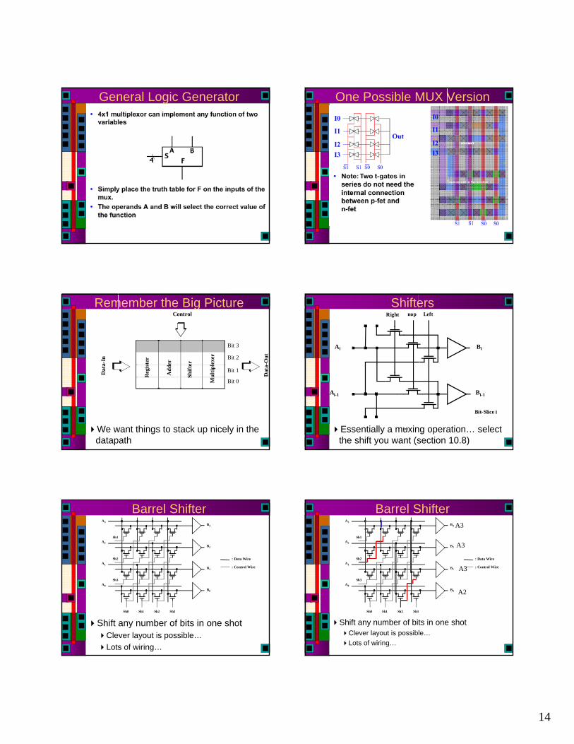
General Logic Generator One Possible MUX Version
Remember the Big Picture
We want things to stack up nicely in the datapath
Bit 3
Bit 2
Bit 1
Bit 0
Reg
ister
Add
er
Shift
er
Mul
tiple
xer
Control
Dat
a-In
Dat
a-O
ut
Tile identical processing elements
Shifters
Essentially a muxing operation… select the shift you want (section 10.8)
Ai
Ai-1
Bi
Bi-1
Right Leftnop
Bit-Slice i
...
Barrel Shifter
Shift any number of bits in one shotClever layout is possible… Lots of wiring…
Sh3Sh2Sh1Sh0
Sh3
Sh2
Sh1
A3
A2
A1
A0
B3
B2
B1
B0
: Control Wire
: Data Wire
Barrel Shifter
Shift any number of bits in one shotClever layout is possible… Lots of wiring…
Sh3Sh2Sh1Sh0
Sh3
Sh2
Sh1
A3
A2
A1
A0
B3
B2
B1
B0
: Control Wire
: Data Wire
A2
A3
A3
A3
15
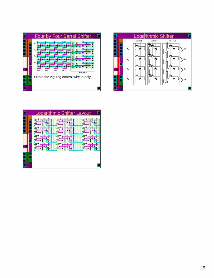
Four by Four Barrel Shifter
Note the zig-zag control wire in polyBuffer
Sh3S h2Sh 1Sh0
A3
A2
A 1
A 0
Logarithmic ShifterSh1 Sh1 Sh2 Sh2 Sh4 Sh4
A3
A2
A1
A0
B1
B0
B2
B3
Logarithmic Shifter Layout


![2’s Complement and Floating-Point - University of …...Two’s Complement •An n-bit, two’s complement number can represent the range [−2!−1, 2 !−1− 1]. • Note the](https://img.pdfslide.net/doc/110x75/5e6c27f608fa3e72a23f5faa/2as-complement-and-floating-point-university-of-twoas-complement-aan.jpg)