Embed Size (px)
Citation preview
HALL ET AL . VOL. 7 ’ NO. 6 ’ 4995–5007 ’ 2013
www.acsnano.org
4995
May 26, 2013
C 2013 American Chemical Society
Broadband Light Absorption withMultiple Surface Plasmon PolaritonWaves Excited at the Interface of aMetallic Grating and Photonic CrystalAnthony Shoji Hall,† Muhammad Faryad,‡ Greg D. Barber,† Liu Liu,§ Sema Erten,‡ Theresa S. Mayer,§
Akhlesh Lakhtakia,‡,* and Thomas E. Mallouk†,*
†Departments of Chemistry, ‡Engineering Science and Mechanics, and §Electrical Engineering, The Pennsylvania State University, University Park,Pennsylvania 16802, United States
Aone-dimensional (1D) metallic grat-ing is an efficient reflector of light,except when the magnetic field vec-
tor of the incident light is parallel to thegrating lines and the angle of incidence θhas a particular value. Then, enhanced lightabsorption arises from the excitation ofcollective oscillations of conduction elec-trons near the grating's surface. The couplinggenerates quasiparticles called surface plas-mons that are confined to the vicinity of themetal/air interface. This resonant phenom-enon can be analyzed classically in terms of asurface plasmon wave by solving Maxwell'sequations for time-harmonic fields. A similar
phenomenon occurs when the air abovethe grating is replaced by a homogeneous,isotropic dielectric material of sufficientthickness. Then the quasiparticles are calledsurface plasmon polaritons (SPP), and theirclassical equivalent is the SPP wave.SPP waves are commonly exploited for
sensing1 and biosensing,2 optical filtering,3
and optical data storage.4 But perhaps theirmost exciting applications in recent yearshave been for photovoltaics,5 photoelectro-chemical cells,6 solar fuel production,7 andsolar thermal photovoltaics.8 Resonant ab-sorptionmanifested as the excitation of SPPwaves has now been investigated for more
* Address correspondence [email protected],[email protected].
Received for review January 22, 2013and accepted May 25, 2013.
Published online10.1021/nn4003488
ABSTRACT
Light incident upon a periodically corrugated metal/dielectric interface can generate surface plasmon polariton (SPP) waves. This effect is used in many
sensing applications. Similar metallodielectric nanostructures are used for light trapping in solar cells, but the gains are modest because SPP waves can be
excited only at specific angles and with one linear polarization state of incident light. Here we report the optical absorptance of a metallic grating coupled
to silicon oxide/oxynitride layers with a periodically varying refractive index, i.e., a 1D photonic crystal. These structures show a dramatic enhancement
relative to those employing a homogeneous dielectric material. Multiple SPP waves can be activated, and both s- and p-polarized incident light can be
efficiently trapped. Many SPP modes are weakly bound and display field enhancements that extend throughout the dielectric layers. These modes have
significantly longer propagation lengths than the single SPP modes excited at the interface of a metallic grating and a uniform dielectric. These results
suggest that metallic gratings coupled to photonic crystals could have utility for light trapping in photovoltaics, sensing, and other applications.
KEYWORDS: surface plasmon polariton wave . photonic crystal . metal grating . photovoltaics . broadband light trapping
ARTIC
LE
HALL ET AL . VOL. 7 ’ NO. 6 ’ 4995–5007 ’ 2013
www.acsnano.org
4996
than three decades as a way of maximizing the con-version of solar light into electricity. It is used in metalgrating-backed thin layers of crystalline silicon (∼5 μmthick)9 and amorphous silicon (∼0.5 μm thick),10 whichcan replace traditionally much thicker (∼100 μm)layers of crystalline silicon.Resonant absorption at the interface of a 1Dmetallic
grating and a homogeneous dielectric material occurswith p-polarized light (i.e., light with its magnetic fieldvector parallel to the grating lines) but not withs-polarized light (electric field vector parallel to thegrating lines).2,11 Thus, the SPP-wave mode is p-polar-ized but cannot be s-polarized. The optical energy isconfined to a subwavelength thickness in the dielectricmaterial,5,11,12 and only a single SPP-wave mode canbe excited at any given free-space wavelength λo overa narrow range of the angle of incidence.1,11 Hence,the experimental absorptance A (A = 1 � R � T, whereR and T are the reflectance and transmittance, respec-tively) of unpolarized broadband light is considerablyless than 50%when a 1Dmetallic grating is employed.5
To address this problem of polarization sensitivity,light-trapping structures that have angular insensitivityand broadband absorption have been researched inrecent years. These structures typically employ two-dimensional (2D) metallic gratings that lower thepolarization sensitivity by converting some of thes-polarized light to p-polarized light.12,17 A strategy todecrease angular sensitivity is to employ metal�insulator�metal (MIM) layers.14�16 However, MIMstructures are highly dissipative because of short SPPwave propagation lengths and large confinementfactors.11 Because of the loss of optical energy withinthe metal, these structures are of limited use forphotovoltaics, which can be efficient only if most ofthe light is absorbed within the semiconductor.9,10
The trapping of light by grating structures canbecome more efficient if the homogeneous dielectricmaterial is replaced by a periodic multilayer, i.e., a 1Dphotonic crystal (PC) with a piecewise homogeneousrefractive index in the thickness direction. In this case,some recent studies have shown that both incidentp- and s-polarized light can excite SPP waves,18,19 evenwhen the wave vector of the incident light is whollyperpendicular to the grating lines. In these reports, themetal/dielectric interface was planar and a prism-coupled configuration,20�22 widely used for opticalsensing, was employed. Only a single p-polarized SPP-wave mode and at most a single s-polarized SPP-wavemode were observed experimentally at any λo withinthe photonic band gap of the periodicmultilayer. How-ever, a theoretical study on a canonical boundary-valueproblem has shown that if the dielectric material has asinusoidally graded refractive index in the thicknessdirection, then multiple p-polarized and multiples-polarized SPP-wave modes can be excited at specificwavelengths with high efficiency.23,24 This prediction
was shown theoretically to holdwell when the periodicdielectric is backed by a metallic grating,25 but it hasnot been experimentally validated.In this paper, we provide the first experimental
evidence that multiple p- and multiple s-polarizedSPP-wave modes can be excited over a broad spectralrange, in a 1DPCbackedby a 1Dmetallic grating. In ourexperiments, the wave vector of the incident light wasoriented perpendicular to grating lines, so that inci-dent p (respectively s)-polarized light could excite onlyp (respectively s)-polarized SPP-wavemodes. The chosenPC was a nonabsorbing, periodic dielectric material oftwo or three periods in thickness. Accompanying theore-tical results show that many of the SPP-wave modesare weakly localized to the interface of the metaland the PC, display field enhancements that spreadthroughout the entire two or three periods of thePC, and have very long propagation lengths (on theorder of hundreds of micrometers). The latter impliesthat less energy will be dissipated in the metal whenthe nonabsorbing dielectric material is replaced by alight absorber, such as the semiconductor layers of a
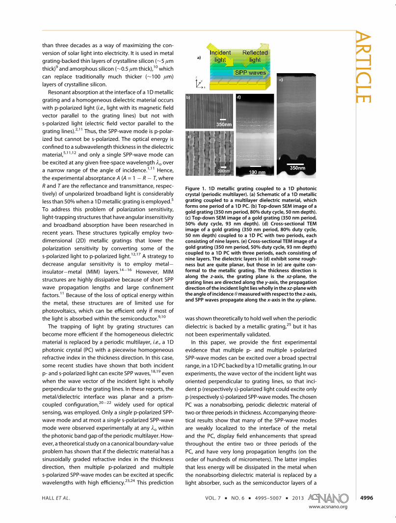
Figure 1. 1D metallic grating coupled to a 1D photoniccrystal (periodic multilayer). (a) Schematic of a 1D metallicgrating coupled to a multilayer dielectric material, whichforms one period of a 1D PC. (b) Top-down SEM image of agold grating (350 nm period, 80% duty cycle, 50 nm depth).(c) Top-down SEM image of a gold grating (350 nm period,50% duty cycle, 93 nm depth). (d) Cross-sectional TEMimage of a gold grating (350 nm period, 80% duty cycle,50 nm depth) coupled to a 1D PC with two periods, eachconsisting of nine layers. (e) Cross-sectional TEM image of agold grating (350 nm period, 50% duty cycle, 93 nm depth)coupled to a 1D PC with three periods, each consisting ofnine layers. The dielectric layers in (d) exhibit some rough-ness but are quite planar, but those in (e) are quite con-formal to the metallic grating. The thickness direction isalong the z-axis, the grating plane is the xz-plane, thegrating lines are directed along the y-axis, the propagationdirection of the incident light lieswholly in the xz-planewiththe angle of incidenceθmeasuredwith respect to the z-axis,and SPP waves propagate along the x-axis in the xy-plane.
ARTIC
LE
HALL ET AL . VOL. 7 ’ NO. 6 ’ 4995–5007 ’ 2013
www.acsnano.org
4997
photovoltaic cell. Not only SPP-wave modes but alsowaveguide modes (whose characteristics dependstrongly on the thickness of the 1D PC)25,26 are excitedand evidently contribute to broadband absorptance.The efficient coupling of light into these structureshas strong implications for performance enhance-ment of sensors,1 photovoltaics,22 and solar thermalphotovoltaics.8
RESULTS AND DISCUSSION
Fabrication of 1D Grating/Periodic Dielectric Structures. Thetest structure used in this study is shown schematicallyin Figure 1a. Here, light is incident from air on a 1D PCthat consists of nine different layers in each periodand is backed by a 1D metallic grating. The dielectriclayer neighboring the grating and filling its troughs ismade of silicon nitride (Si3N4); the next seven layers aremade of silicon oxynitride {(Si3N4)a(SiO2)1�a}, eachwith a different value of a; and the ninth (top) layer ismade of silicon oxide (SiO2). Figure SI-1 gives the mea-sured refractive indexes of all nine dielectric materialsas functions of λo. The imaginary part of the refractiveindex was below 10�4 in the spectral regime studiedfor all the dielectric materials, and it was thereforeignored in the calculations.
Top-down scanning electron microscope (SEM)images and cross-sectional transmission electron mi-croscope (TEM) images of structures fabricated andcharacterized in this study are shown in Figure 1b�e.Whereas the vapor-deposited dielectric layers in theshallow grating structure shown in Figure 1d appearmore or less planar, those shown in Figure 1e, which is
a structure with a deeper metallic grating, are moreconformal.
Due to the periodicity of the metallic grating, theBloch theorem27,28 mandates that the reflected andthe transmitted fields must contain both specular andnonspecular components when the structure is illumi-nated by a monochromatic plane wave. Furthermore,the fields induced inside the structure must consist ofFloquet harmonics of negative, zero, and positive orders.29
It is the panoply of Fourier harmonics that facilitates theexcitation of multiple SPP-wave modes in the grating-coupled configuration under investigation.30�32 Be-cause the metallic gratings are ∼200 nm thick, theydo not transmit light in the wavelength range studiedand hence T = 0 in all experiments.
Calculations of the reflected field were made for0�e θe 70� (where 0� is defined as normal incidence)for λo between 400 and 1000 nm using the rigorouscoupled wave approach.25,29 The measured complexrefractive index of gold, shown in Figure SI-2, was usedin the calculations along with the data in Figure SI-1 forthe dielectric materials. Over most of the θ � λodomain chosen for the calculations and for incidentlight of both p- and s-polarization states, the nonspe-cular reflected components were very weak for thestructure that has a shallow grating (Figure 1d), ascan be deduced from comparing Figures 2 and SI-3.Accordingly, only the specular reflectances R0p andR0s were measured at angles between 8� and 55� inorder to determine the absorptances Ap≈ 1� R0p andAs≈ 1� R0s. We calculated absorptances for the struc-ture shown in Figure 1d when the PC contained either
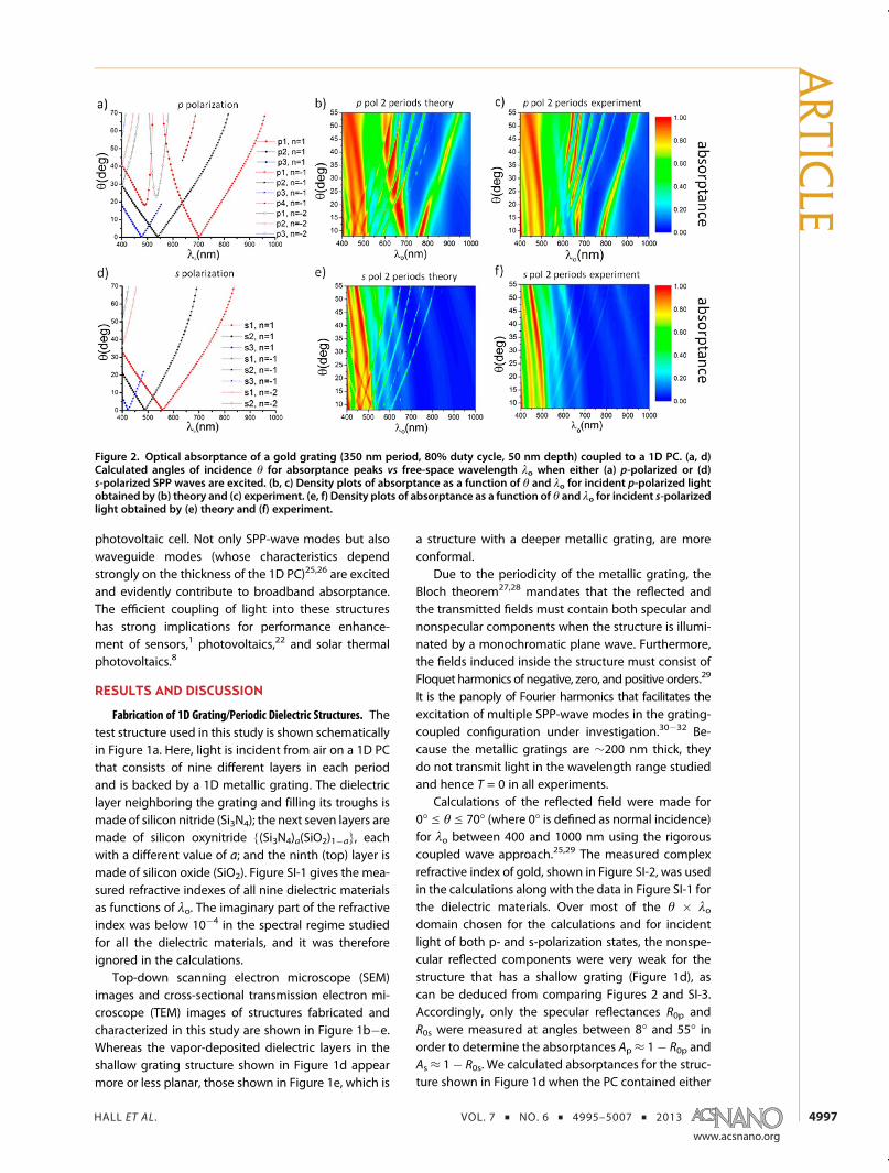
Figure 2. Optical absorptance of a gold grating (350 nm period, 80% duty cycle, 50 nm depth) coupled to a 1D PC. (a, d)Calculated angles of incidence θ for absorptance peaks vs free-space wavelength λo when either (a) p-polarized or (d)s-polarized SPP waves are excited. (b, c) Density plots of absorptance as a function of θ and λo for incident p-polarized lightobtained by (b) theory and (c) experiment. (e, f) Density plots of absorptance as a function of θ and λo for incident s-polarizedlight obtained by (e) theory and (f) experiment.
ARTIC
LE
HALL ET AL . VOL. 7 ’ NO. 6 ’ 4995–5007 ’ 2013
www.acsnano.org
4998
two or three periods. Peaks in the plots of Ap and As vs
θ (respectively λo) for fixed λo (respectively θ) wereidentified. Each absorptance peak whose λo location(at a fixed θ) or θ location (at a fixed λo) dependedvery weakly on the number of periods of the PCbeyond a threshold indicated the excitation of anSPP-wave mode, which we then confirmed by thesolution of a canonical boundary-value problem.21,27
At a fixed λo, we also determined the order n of theFloquet harmonic corresponding to each excitedSPP-wave mode from the canonical boundary-valueproblem.25,31
Excitation of Multiple SPP Waves in Shallow 1D GratingStructures. Figure 2 compares experimental and theo-retical results for a gold metallic grating with a periodof 350 and 50 nm tall rectangular raised sections thatspan 80% (duty cycle) of each period. The metallicgrating is shown alone in Figure 1b, and the entirestructure comprising the grating and the PC is shownin cross-section in Figure 1d. Figure 2a and d showthe calculated θ locations and λo locations of p- ands-polarized SPP-wave modes for λo between 400 and1000 nm.21,27 As many as 10 p- and eight s-polarizedSPP-wave modes are theoretically possible for thisstructure. Density plots of theoretically predicted andexperimentally measured absorptances as functionsof θ and λo are presented in Figure 2b,c and 2e,f for
incident p- and s-polarized light, respectively, for thetwo-period PC backed by the grating.
The loci of absorptance peaks in the contour plotsin Figure 2b,c closely resemble the lines in Figure 2a,and the same statement can be made for Figure 2e,fand 2d. Remarkably, the experimental data confirm theexistence of nine of 10 p-polarized SPP-wave modespredicted theoretically. All four modes identified byn = �1, two of three modes identified by n = þ1, andone of three modes identified by n = �2 in Figure 2aare clearly evident in Figure 2c. The existence of thetwo other modes identified by n =�2 in Figure 2a canbe discerned experimentally in a high-resolution ver-sion of Figure 2c, but their excitation is weak becauseof the strong background absorption at λo < 500 nmcaused by waveguide modes superimposed on theinterband transitions of gold.11 The onset of gold'sinterband transitions lies below λo < 600 nm, but thetransitions do not completely dominate the signaluntil λo < 500. In contrast, the experimental dataconfirm the existence of only two of eight s-polarizedSPP-wave modes. Both of these modes are identifiedby n = �1 in Figure 2f. Both theory and experimentindicate that s-polarized SPP-wave modes are excitedweakly in comparison to the p-polarized SPP-wavemodes in the structure of Figure 1d. This suggests thatthis structure is not very efficient in using incident
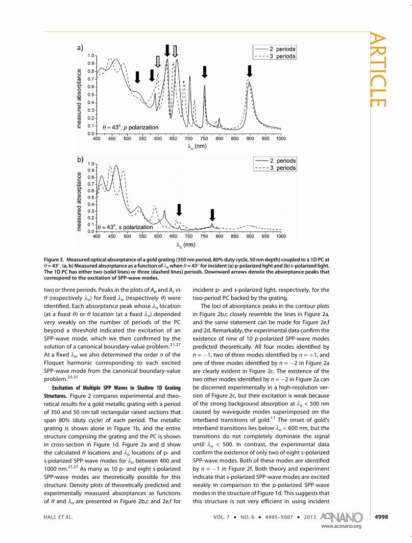
Figure 3. Measured optical absorptance of a gold grating (350 nmperiod, 80%duty cycle, 50 nmdepth) coupled to a 1DPC atθ= 43�. (a, b) Measured absorptance as a function of λo when θ= 43� for incident (a) p-polarized light and (b) s-polarized light.The 1D PC has either two (solid lines) or three (dashed lines) periods. Downward arrows denote the absorptance peaks thatcorrespond to the excitation of SPP-wave modes.
ARTIC
LE
HALL ET AL . VOL. 7 ’ NO. 6 ’ 4995–5007 ’ 2013
www.acsnano.org
4999
s-polarized light to excite SPP-wave modes. Thisconclusion holds even when the number of periodsof the PC is increased from two to three, as can beseen by comparing the density plots in Figure 2b,c,
e,f (two periods) with their counterparts in Figure SI-4(three periods).
Differentiating p- and s-Polarized SPP Modes from WaveguideModes. To provide greater clarity about the excitation
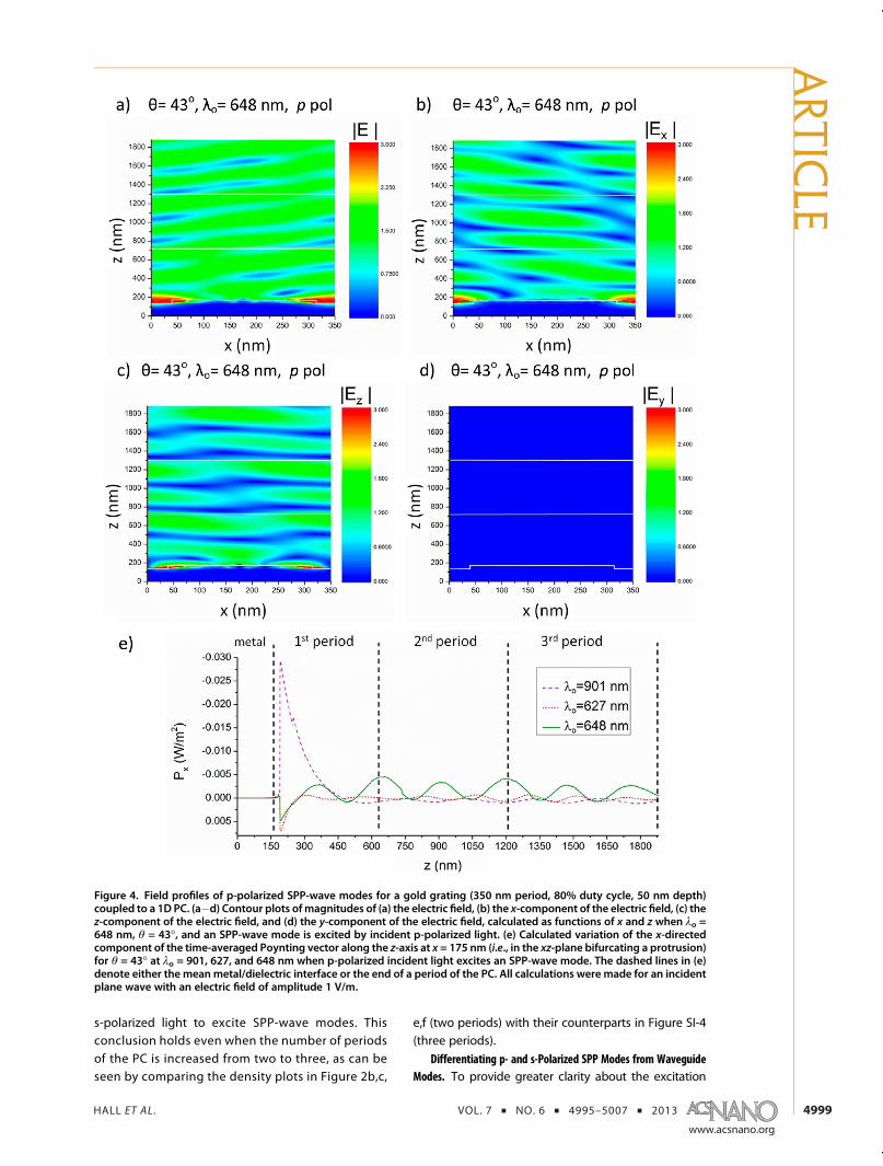
Figure 4. Field profiles of p-polarized SPP-wave modes for a gold grating (350 nm period, 80% duty cycle, 50 nm depth)coupled to a 1D PC. (a�d) Contour plots ofmagnitudes of (a) the electric field, (b) the x-component of the electric field, (c) thez-component of the electric field, and (d) the y-component of the electric field, calculated as functions of x and z when λo =648 nm, θ = 43�, and an SPP-wave mode is excited by incident p-polarized light. (e) Calculated variation of the x-directedcomponent of the time-averaged Poynting vector along the z-axis at x = 175 nm (i.e., in the xz-plane bifurcating a protrusion)for θ = 43� at λo = 901, 627, and 648 nm when p-polarized incident light excites an SPP-wave mode. The dashed lines in (e)denote either the mean metal/dielectric interface or the end of a period of the PC. All calculations were made for an incidentplane wave with an electric field of amplitude 1 V/m.
ARTIC
LE
HALL ET AL . VOL. 7 ’ NO. 6 ’ 4995–5007 ’ 2013
www.acsnano.org
5000
ofmultiple SPP-wavemodeswith respect to thenumberof periods in the PC, experimentally measured andtheoretically predicted absorptances are presented asfunctions of λo for θ = 43�. These absorptances areshown for two- and three-period PCs in Figures 3 andSI-5, respectively. Every absorptance peak whose θ
location at fixed λo remains invariant with the additionof the third period of the photonic crystal definitelycorresponds to the excitation of SPP-wave modes.Conversely, the peaks whose θ-values are highly sensi-tive to the total thickness of the PC are waveguidemodes.25 The energy of an SPP-wave mode is localized,weakly or strongly, to the metal/dielectric interface,but the energy of a waveguide mode is more evenlydistributed throughout the thickness of the dielectriclayers. Downward arrows in Figures 3a and SI-5a identifyfive p-polarized SPP-wave modes for λo > 500 nm. Theinterband transitions of gold11 prevent the resolution ofSPP-wave modes at wavelengths shorter than 500 nm.The broad peak at λo = 520 nm corresponds to the
excitation of two co-propagating SPP-wave modes asFloquet harmonics of orders n = 1 and n = �2. For thepurpose of comparison, the measured absorptance of aflat gold film with two or three periods of the PC ispresented in Figure SI-6. No invariant peaks are ob-served, because only waveguide modes can be excitedwhen the grating is absent. Furthermore, the absorp-tance of this control sample is nearly null for bothpolarization states for λo > 600 nm, indicating that thePC or Fabry�Perot interference modes do not give riseto significant absorption of light at wavelengths longerthan the interband transitions of gold.
Inspection of Figures 3 and SI-5 reveals that someSPP-wave modes shift slightly with the addition of athird period to the PC. In Figure 3a, we observe an SPP-wave mode in the vicinity of λo ≈ 600 nm that is notevident unless three periods of the PC are presentabove the metallic grating. Furthermore, in the samefigure we observe a significant shift of an SPP-wavemode from λo = 660 nm to λo = 648 nm when the
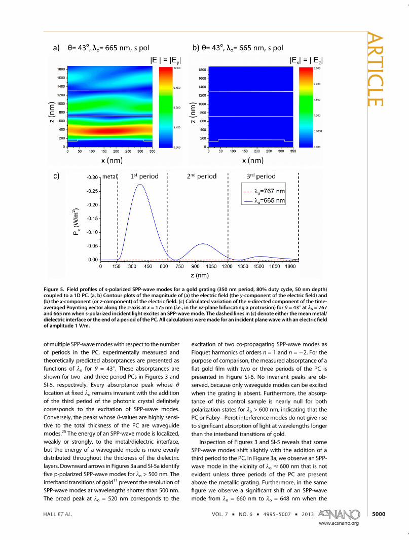
Figure 5. Field profiles of s-polarized SPP-wave modes for a gold grating (350 nm period, 80% duty cycle, 50 nm depth)coupled to a 1D PC. (a, b) Contour plots of the magnitude of (a) the electric field (the y-component of the electric field) and(b) the x-component (or z-component) of the electric field. (c) Calculated variation of the x-directed component of the time-averaged Poynting vector along the z-axis at x = 175 nm (i.e., in the xz-plane bifurcating a protrusion) for θ = 43� at λo = 767and 665 nmwhen s-polarized incident light excites an SPP-wavemode. The dashed lines in (c) denote either themeanmetal/dielectric interface or the end of a period of the PC. All calculations weremade for an incident planewavewith an electric fieldof amplitude 1 V/m.
ARTIC
LE
HALL ET AL . VOL. 7 ’ NO. 6 ’ 4995–5007 ’ 2013
www.acsnano.org
5001
thickness of the PC is increased from two to threeperiods. These SPP-wave modes, denoted by openarrows in Figure 3, are weakly localized to the metal/dielectric interface and, therefore, are highly sensitiveto the dielectric environment above the metallic grat-ing. Figure 4a�d show the calculated spatial profiles ofthemagnitudes of the components of the electric field.It is evident that the SPP-wave modes excited withp-polarized light do not contain any electric fieldoriented parallel to the y-direction; therefore SPPwaves excited with p-polarized light are completelyp-polarized in nature. Although the contour plots showthat the electric field strength is maximized near thecorners of the metallic grating, a significant portion ofthe field extends into all three periods of the dielectricstack. Figure 4e shows the variation along the thicknessdirection (z-axis) of the component of the time-aver-aged Poynting vector in the direction of propagation,taken at a slice through the middle of the grating (x =175 nm, x-axis) for the SPP-wave modes at λo = 648,627, and 901 nm for the three-period PC. The SPP-wavemodes at λo = 627 and 901 nm are localized to themetal/dielectric interface, decaying within ∼270and ∼75 nm, respectively, into the first period of thePC. Thesemodes shift only slightlywhen the number ofperiods of the PC is increased from two to three,consistent with their localization to the metal/PC inter-face. In contrast, the SPP-wave mode at λo = 648 nmexhibits a large shift because its Poynting vector isdistributed into all three layers of the PC.
The absorptance peaks identified by downwardarrows in Figures 3b and SI-6b indicate the excitationof two different s-polarized SPP-wavemodes at θ= 43�.An SPP-wave mode in Figure 3b at λo = 660 nm whenthe PC has two periods blue-shifts to λo = 655 nm withthe addition of a third period. From Figure 5b, it is clearthat this SPP-wave mode is completely s-polarizedsince its Ex and Ez components are zero. Figure 5cpresents the variation along z of the x-directed com-ponent of the time-averaged Poynting vector of thisSPP-wavemode and an SPP-wavemode at λo = 665 nmfor the three-period structure. As expected from thesignificant blue shift, this SPP-wave mode is weaklylocalized to the metal/dielectric interface. The electricfield has amaximummagnitude not in themean planeof the periodically corrugated metal/dielectric inter-face but in the middle of the first period of the di-electric. This characteristic is very different from that ofthe p-polarized SPP-wave modes in Figure 4c. The x-directed component of the time-averaged Poyntingvector of the SPP-wave mode at λo = 767 nm is verysmall because it is weakly excited.
Each panel in Figure 2 shows that different SPP-wave modes can be excited at a single λo by lightincident at different angles. For instance, when λo =668 nm, two p- and two s-polarized SPP-wave modesare excited, as shown in Figure 6. Correspond-ing plots of calculated absorptances are shown inFigure SI-7. These SPP-wavemodes differ in phase speedvp = c/[(nλo/L) þ sin θ], where L is the period of the
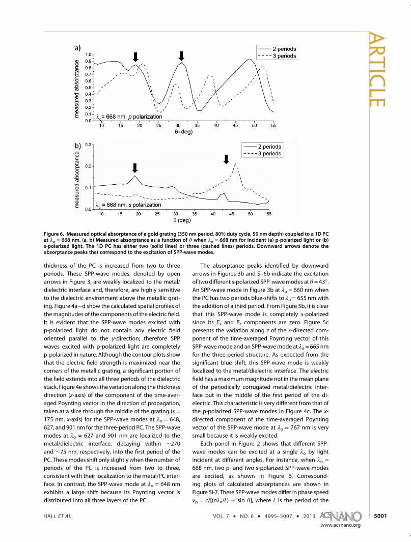
Figure 6. Measured optical absorptance of a gold grating (350 nm period, 80% duty cycle, 50 nm depth) coupled to a 1D PCat λo = 668 nm. (a, b) Measured absorptance as a function of θ when λo = 668 nm for incident (a) p-polarized light or (b)s-polarized light. The 1D PC has either two (solid lines) or three (dashed lines) periods. Downward arrows denote theabsorptance peaks that correspond to the excitation of SPP-wave modes.
ARTIC
LE
HALL ET AL . VOL. 7 ’ NO. 6 ’ 4995–5007 ’ 2013
www.acsnano.org
5002
grating, as they are excited at different angles ofincidence as Floquet modes of different orders n, cbeing the speed of light in free space. An increase inthe number of periods in the PC can cause a smallincrease or decrease in θ for the excitation of a certainSPP-wave mode, but that value of θ stabilizes after thenumber of periods crosses a threshold, according totheoretical data shown in a previous paper.20
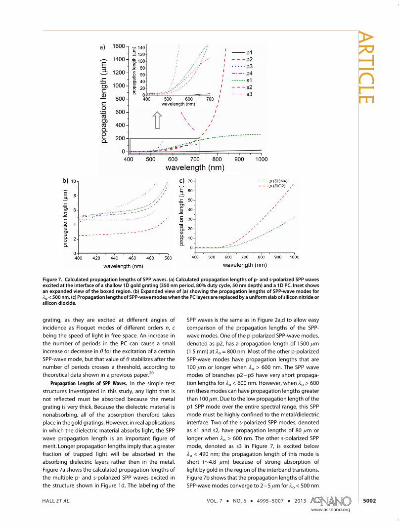
Propagation Lengths of SPP Waves. In the simple teststructures investigated in this study, any light that isnot reflected must be absorbed because the metalgrating is very thick. Because the dielectric material isnonabsorbing, all of the absorption therefore takesplace in the gold gratings. However, in real applicationsin which the dielectric material absorbs light, the SPPwave propagation length is an important figure ofmerit. Longer propagation lengths imply that a greaterfraction of trapped light will be absorbed in theabsorbing dielectric layers rather then in the metal.Figure 7a shows the calculated propagation lengths ofthe multiple p- and s-polarized SPP waves excited inthe structure shown in Figure 1d. The labeling of the
SPP waves is the same as in Figure 2a,d to allow easycomparison of the propagation lengths of the SPP-wave modes. One of the p-polarized SPP-wave modes,denoted as p2, has a propagation length of 1500 μm(1.5 mm) at λo = 800 nm. Most of the other p-polarizedSPP-wave modes have propagation lengths that are100 μm or longer when λo > 600 nm. The SPP wavemodes of branches p2�p5 have very short propaga-tion lengths for λo < 600 nm. However, when λo > 600nm thesemodes can have propagation lengths greaterthan 100 μm. Due to the low propagation length of thep1 SPP mode over the entire spectral range, this SPPmode must be highly confined to the metal/dielectricinterface. Two of the s-polarized SPP modes, denotedas s1 and s2, have propagation lengths of 80 μm orlonger when λo > 600 nm. The other s-polarized SPPmode, denoted as s3 in Figure 7, is excited belowλo < 490 nm; the propagation length of this mode isshort (∼4.8 μm) because of strong absorption oflight by gold in the region of the interband transitions.Figure 7b shows that the propagation lengths of all theSPP-wave modes converge to 2�5 μm for λo < 500 nm
Figure 7. Calculated propagation lengths of SPP waves. (a) Calculated propagation lengths of p- and s-polarized SPP wavesexcited at the interface of a shallow 1D gold grating (350 nm period, 80% duty cycle, 50 nm depth) and a 1D PC. Inset showsan expanded view of the boxed region. (b) Expanded view of (a) showing the propagation lengths of SPP-wave modes forλo < 500 nm. (c) Propagation lengths of SPP-wavemodeswhen the PC layers are replacedby a uniform slab of silicon nitride orsilicon dioxide.
ARTIC
LE
HALL ET AL . VOL. 7 ’ NO. 6 ’ 4995–5007 ’ 2013
www.acsnano.org
5003
because of this effect; an expanded view of this regionis shown in Figure 7b. Figure 7c shows the propagationlengths for a structure in which the PC is replaced by auniform slab of silicon oxide or silicon nitride. In thiscase, the propagation lengths are shorter than 100 μmacross the entire spectral range of interest. The im-portant conclusion is that multiple SPP modes gener-ated in the PC can propagate farther because lightis not, in general, as strongly localized to the metal/dielectric interface as it is in uniformdielectric structures.
Excitation of s- and p-Polarized SPP Waves in Deep 1D GratingStructures. The experimental and theoretical resultsdescribed heretofore establish the broadband excita-tion of multiple SPP-wave modes using both p- ands-polarized light, but the latter modes are quite weakand are therefore of limited utility for light trapping inthe dielectric layers. In order to improve the excitationefficiency of the s-polarized SPP-wave modes, weredesigned the gold grating to have 93 nm depthand 50% duty cycle, keeping the grating period L stillfixed at 350 nm (Figure 1c).When the PCwas depositedon this grating, the dielectric layers conformed to the
grating's corrugations, as shown in Figure 1e for athree-period PC.
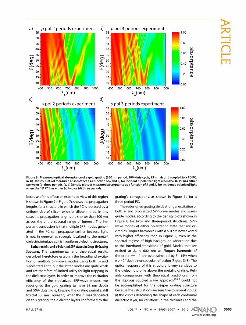
The redesigned grating yields stronger excitation ofboth s- and p-polarized SPP-wave modes and wave-guide modes, according to the density plots shown inFigure 8 for two- and three-period structures. SPP-wave modes of either polarization state that are ex-cited as Floquet harmonics with n > 0 are now excitedwith higher efficiency than in Figure 2, even in thespectral regime of high background absorption dueto the interband transitions of gold. Modes that areexcited at λo < 600 nm as Floquet harmonic ofthe order n= �1 are overestimated by 5�15% whenθ > 40� due to nonspecular reflection (Figure SI-8). Theoptical response of this structure is very sensitive tothe dielectric profile above the metallic grating. Reli-able comparisons with theoretical predictions fromthe rigorous coupled wave approach25,29 could notbe accomplished for the deeper grating structurebecause the calculations are sensitive to several inputs:(i) the curves describing the shape of each conformaldielectric layer, (ii) variations in the thickness and the
Figure 8. Measured optical absorptance of a gold grating (350 nm period, 50% duty cycle, 93 nm depth) coupled to a 1D PC.(a, b) Density plots ofmeasured absorptance as a function of θ and λo for incident p-polarized light when the 1D PC has either(a) two or (b) three periods. (c, d) Density plots ofmeasured absorptance as a function of θ and λo for incident s-polarized lightwhen the 1D PC has either (c) two or (d) three periods.
ARTIC
LE
HALL ET AL . VOL. 7 ’ NO. 6 ’ 4995–5007 ’ 2013
www.acsnano.org
5004
composition of each dielectric layer from one unit cellto another, and (iii) the aperiodicity of the corrugations
of the metallic grating. A more realistic model wouldrequire several unit cells of the structure to be treated
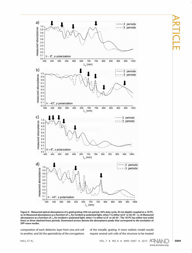
Figure 9. Measured optical absorptance of a gold grating (350 nm period, 50% duty cycle, 93 nm depth) coupled to a 1D PC.(a, b) Measured absorptance as a function of λo for incident p-polarized light, when θ is either (a) 8� or (b) 43�. (c, d) Measuredabsorptance as a function of λo for incident s-polarized light, when θ is either (c) 8� or (d) 43�. The 1D PC has either two (solidlines) or three (dashed lines) periods. Downward arrows denote the absorptance peaks that correspond to the excitation ofSPP-wave modes.
ARTIC
LE
HALL ET AL . VOL. 7 ’ NO. 6 ’ 4995–5007 ’ 2013
www.acsnano.org
5005
as one unit cell, but then computations could notbe made within a reasonable period of time. Thesedifficulties notwithstanding, theoretical contour plotsfor samples with two periods of the PC, calculated on
the basis of the simple unit cell, are presented inFigure SI-9.
Figure 9 shows the measured absorptances Ap andAs as functions of λo for θ = 8� and θ = 43� for two- and
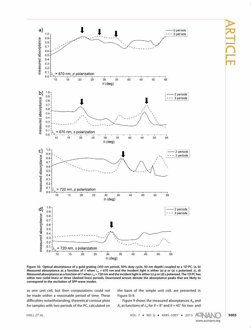
Figure 10. Optical absorptance of a gold grating (350 nm period, 50% duty cycle, 93 nm depth) coupled to a 1D PC. (a, b)Measured absorptance as a function of θ when λo = 670 nm and the incident light is either (a) p or (a) s polarized. (c, d)Measured absorptance as a functionofθwhen λo = 720nmand the incident light is either (c) p or (d) s polarized. The 1DPChaseither two (solid lines) or three (dashed lines) periods. Downward arrows denote the absorptance peaks that are likely tocorrespond to the excitation of SPP-wave modes.
ARTIC
LE
HALL ET AL . VOL. 7 ’ NO. 6 ’ 4995–5007 ’ 2013
www.acsnano.org
5006
three-period PC structures. Similar plots, but as func-tions of θ for λo = 670 nm and λo = 720 nm, areprovided in Figure 10. Four p-polarized SPP-wavemodes and five s-polarized SPP-wave modes are ex-cited at θ = 8�; likewise, five p-polarized and threes-polarized SPP-wave modes are excited at θ = 43�.More p-polarized SPP-wave modes are excited athigher θ, but more s-polarized SPP modes are excitedat lower θ.
Figure 10 shows that two p- and two s-polarizedSPP-wave modes are excited at λo = 670 nm, butonly one SPP-wave mode of each polarization state isexcited at λo = 720 nm. The excitation efficiencies ofthe s-polarized SPP-wavemodes are higher at lower λo.Importantly, while the excitation efficiencies of the s-polarized SPP-wave modes are not as high as those ofthe p-polarized SPP-wave modes, they are clearlymuch higher than those of the s-polarized SPP-wavemodes in the shallow grating structure shown inFigure 1d. Indeed, we conclude from Figures 8, 9,and 10 that the excitation efficiencies of s-polarizedSPP-wave modes in the deeper grating structure ofFigure 1e can approach 100% (i.e., As ≈ 1.0). It is alsolikely that the redesigned structure supports moreSPP-wave modes than identified in these figures. Theweakly bound SPP-wave modes that are not invariantwith the PC thickness require more accurate theore-tical modeling to confirm their existence.
CONCLUSIONS
We have theoretically modeled and experimentallydemonstrated a newapproach for broadband trapping
of light as SPP-wavemodes: an appropriately designedmetallic-grating-backed periodic dielectric multilayersupports the existence of multiple SPP-wave modes33
of both p- and s-polarization states over a wide spec-trum of free-space wavelengths. Significantly, we havesuccessfully demonstrated that with proper designs-polarized SPP-wave modes can be excited with highefficiency.Solution of the time-harmonic Maxwell equations
indicates that the fields of several SPP-wavemodes areweakly localized to the periodically corrugated metal/dielectric interface. The weakness of the localizationimplies that the incident light energy can be moreevenly distributed in a light-absorbing PC that is theactive component of a sensor or solar cell. The longpropagation lengths of many of the multiple SPPwaves also indicate that less energy is dissipated inthe metallic layer relative to structures with uniformdielectrics. Theory shows that the relationship be-tween the number of SPP-wave modes that can beexcited in a given spectral regime and the period of thePC is somewhat complicated.24 In this initial experi-mental study, we found that multiple SPP-wavemodesare excited in a range of free-space wavelengths λocomparable to the period of the PC. This effect remainsto be explored and optimized for specific applications.Thematerials used in this study are commonplace in
nanotechnology. Given the broad interest in plasmonicnanostructures and photonic crystals, which can befabricated from many different materials, the synergythat arises from their combination should be useful inmany future optical applications.
MATERIALS AND METHODSFabrication of Metallic Gratings. Metallic gratings were fabri-
cated as described in detail elsewhere.34 In brief, silicon waferswere patterned by electron beam lithography on ZEP520Aphotoresist (Zeon, Tokyo) with the inverse pattern of thedesired metallic grating. The pattern in the photoresist wastransferred into the silicon by inductively coupled reactive ionetching on a Versalock 700 (Plasma-Therm, St. Petersburg, FL,USA) with pure Cl2 gas. The photoresist dissolved in Nanostrip,a commercially available resist remover, with the assistance ofa bath sonicator. Gold was thermally evaporated on the pat-terned silicon wafer at room temperature with a base pressureof <1 � 10�6 at 0.1 nm/s. The gold film was attached to a glassslide using EpoTek 377 epoxy (Epoxy Technology, Billerica, MA,USA). The epoxy resin was cured by a seven-day thermaltreatment at 125 �C. The gold film was released from the siliconwafer with a razor blade, yielding a gold grating glued to a glassslide. All gratings used in this work were 6 � 6 mm in size.
Fabrication of Periodic Dielectric Multilayers. Periodic multilayersof silicon oxide/oxynitride were grown directly on the goldgratings by plasma-enhanced chemical vapor deposition ona Cluster Tool (Applied Materials, Santa Clara, CA, USA) at asusceptor temperature of 220 �C. Ammonia, silane, and nitrousoxide were used in varying ratios to deposit layers with specificrefractive indices. All layers were deposited at a pressure of3.5 Torr and a power density of 0.955 W/cm2.
Electron Microscopy. SEM images were collected on a Leo 1530FESEM (Carl Zeiss, Oberkochen, Germany), and TEM images
were collected on a Phillips 420 TEM (Phillips, Amsterdam, TheNetherlands).
Optical Characterization of Dielectric and Gold Layers. The complexrefractive index of each layer, whether dielectric or metallic, wascalculated from data obtained by using an RC2 spectroscopicellipsometer (Woollam, Lincoln, NE, USA). For these measure-ments, a thin film of the same nominal thickness and composi-tion as those grown for the multilayer structures (Figure 1) wasdeposited under identical conditions on a glass slide or siliconwafer. The spot sizeused for collectionof thedatawas3.5� 3.5mm.
Parameters for Theoretical Simulations. For computation of ab-sorptances using the rigorous coupled wave approach of thestructure containing gold gratings of 350 nm period, 80% dutycycle, and 50 nm depth, the unit cell profile of the gratings wasapproximated by a sinusoid, as suggested by cross-sectional views(not presented) of the grating shown in Figure 1b. The gratingregionwas divided into 2 nm thick slices parallel to themean planeof themetal/dielectric interface, andeach slicewas considered tobehomogeneous. For computations, 31 Floquet harmonicswere used.
Measurements of Specular and Nonspecular Reflectances. Specularreflectance measurements were performed on a Lambda 950UV�visible spectrometer (Perkin-Elmer, Waltham, MA, USA)with a Universal Reflectance accessory. Measurements wereperformed in steps of 1 nm for λo and 1� for θ. The nonspecularreflectance of order�1 was measured using a dual rotary stagearrangement. Monochromatic light, in 5 nm intervals, was selectedfrom a broadband source (150 W Xe arc lamp, Oriel-Newport)through a single pass monochromator. The intensity of the
ARTIC
LE
HALL ET AL . VOL. 7 ’ NO. 6 ’ 4995–5007 ’ 2013
www.acsnano.org
5007
monochromatic beam was determined from the specular re-flectance from a calibrated silver mirror in place of the gratingand a silicon photodiode (Hamamatsu Corporation, S1226-44BQ, 3.6 mm � 3.6 mm) at a nominal distance of 110 mmfrom the mirror/grating plane. At this distance, the siliconphotodiode detector occupies a subtended angle of approxi-mately 1.9�. The intensity of the nonspecular,�1 order reflectedlight was measured using the same silicon photodiode. Theintensity of the nonspecularly reflected light was obtained fromthe ratio of the grating-detector current to the calibratedcurrent measured from the Ag mirror.
Conflict of Interest: The authors declare no competingfinancial interest.
Acknowledgment. We thank Trevor Clark, Josh Maier, andDimitri Vaughn for assistance with transmission electron micro-scopy. We also gratefully acknowledge helpful discussions withPeterMonk andManuel Solano. This workwas supported by theNational Science Foundation under grant no. DMR-1125591.Fabrication experiments were performed at the PennsylvaniaState University Materials Research Institute NanofabricationLaboratory, which is supported by the National Science Foun-dation under Cooperative Agreement No. ECS-0335765. A.L. isalso grateful to Charles Godfrey Binder Endowment at thePennsylvania State University for partial support of this work.
Supporting Information Available: Definition of a surfaceplasmon polariton wave, refractive index vs wavelength datafor metal and dielectric layers, nonspecular reflectance data,reflectance data for three-period photonic crystals on goldgratings, calculated absorptance spectra for two- and three-period photonic crystals on shallow gold gratings, experimentalabsorptance spectra for photonic crystals on flat gold sub-strates, and absorptance spectra of photonic crystals on deepgold gratings. This material is available free of charge via theInternet at http://pubs.acs.org.
REFERENCES AND NOTES1. Homola, J.; Yee, S. S.; Gauglitz, G. Surface Plasmon Reso-
nance Sensors: Review. Sens. Actuators, B 1999, 54, 3–15.2. Abdulhalim, I.; Zourob, M.; Lakhtakia, A. Surface Plasmon
Resonance for Biosensing: A Mini-Review. Electromag-netics 2008, 28, 214–242.
3. Dandin, M.; Abshire, P.; Smela, E. Optical Filtering Tech-nologies for Integrated Fluorescence Sensors. Lab Chip2007, 7, 955–977.
4. Zia, R.; Selker, M. D.; Catrysse, P. B.; Brongersma, M. L.Geometries and Materials for Subwavelength SurfacePlasmon Modes. J. Opt. Soc. Am. A 2004, 21, 2442–2446.
5. Atwater, H. A.; Polman, A. A. Plasmonics for ImprovedPhotovoltaic Devices. Nat. Mater. 2010, 9, 205–213.
6. Nishijima, Y.; Nishijima, Y.; Ueno, K.; Kotake, Y.; Murakoshi,K.; Inoue, H. Misawa. Near-Infrared Plasmon-AssistedWater Oxidation. J. Phys. Chem. Lett. 2012, 3, 1248–1252.
7. Ingram, D. B.; Linic, S. Water Splitting on CompositePlasmonic-Metal/Semiconductor Photoelectrodes: Evi-dence for Selective Plasmon-Induced Formation of ChargeCarriers Near the Semiconductor Surface. J. Am. Chem. Soc.2011, 14, 5202–5205.
8. Nagpal, P.; Han, S. E.; Stein, A.; Norris, D. J. Efficient Low-Temperature Thermophotovoltaic Emitters from MetallicPhotonic Crystals. Nano Lett. 2008, 8, 3238–3243.
9. Heine, C.; Morf, R. H. Submicrometer Gratings for SolarEnergy Applications. Appl. Opt. 1995, 34, 2476–2482.
10. Sheng, P.; Bloch, A. N.; Stepleman, R. S. Wavelength-Selective Absorption Enhancement in Thin-Film SolarCells. Appl. Phys. Lett. 1983, 43, 579–581.
11. Maier, S. A. Plasmonics�Fundamentals and Applications;Springer: New York, 2007.
12. McPheeters, C. O.; Yu, E. T. Computational Analysis of ThinFilm InGaAs/GaAsQuantumWell Solar Cells with Back SideLight Trapping Structures. Opt. Express 2012, 20, 864–878.
13. Landy, N. I.; Sajuyigbe, S.; Mock, J. J.; Smith, D. R.; Padilla,W. J. A. Perfect Metamaterial Absorber. Phys. Rev. Lett.2008, 100, 207402.
14. Liu, N.; Mesch, M.; Weiss, T.; Hentschel, M.; Giessen, H.Infrared Perfect Absorber and Its Application as PlasmonicSensor. Nano Lett. 2010, 10, 2342–2348.
15. Tittl, A.; Mai, P.; Taubert, R.; Dregely, D.; Liu, N.; Giessen, H.Palladium-Based Plasmonic Perfect Absorber in the VisibleWavelength Range and Its Application to Hydrogen Sen-sing. Nano Lett. 2011, 11, 4366–4369.
16. Aydin, K.; Ferry, V. E.; Briggs, R. M.; Atwater, H. A. BroadbandPolarization-Independent Resonant Light AbsorptionUsing Ultrathin Plasmonic Super Absorbers.Nat. Commun.2011, 2, 517.
17. Hooper, I. R.; Sambles, J. R. Surface Plasmon Polaritons onNarrow-Ridged Short-Pitch Metal Gratings in the ConicalMount. J. Opt. Soc. Am. A 2003, 20, 836–843.
18. Salamon, Z.; Macleod, H. A.; Tollin, G. Coupled Plasmon-Waveguide Resonators: A New Spectroscopic Tool forProbing Proteolipid Film Structure and Properties. Bio-phys. J. 1997, 73, 2791–2797.
19. Salamon, Z.; Tollin, G. Optical Anisotropy in Lipid BilayerMembrane: Coupled Plasmon-Waveguide ResonanceMeasurements of Molecular Orientation, Polarizability,and Shape. Biophys. J. 2001, 80, 1557–1567.
20. Turbadar, T. Complete Absorption of Light by Thin MetalFilms. Proc. Phys. Soc. London 1959, 73, 40–44.
21. Kretschmann, E.; Raether, H. Radiative Decay of Non-Radiative Surface Plasmons Excited by Light. Z. Natur-forsch. A 1968, 23, 2135–2136.
22. Otto, A. Excitation of Nonradiative Surface Plasma Wavesin Silver by the Method of Frustrated Total Reflection.Z. Phys. 1968, 216, 390–410.
23. Faryad, M.; Lakhtakia, A. On Surface Plasmon-PolaritonWaves Guided by the Interface of a Metal and a RugateFilter with a Sinusoidal Refractive-Index Profile. J. Opt. Soc.Am. B 2010, 27, 2218–2223.
24. Atalla, M. R. M.; Faryad, M.; Lakhtakia, A. On Surface-Plasmon-Polariton Waves Guided by the Interface of aMetal and a Rugate Filter with a Sinusoidal Refractive-Index Profile. Part II: High-Phase-Speed Solutions. J. Opt.Soc. Am. B 2012, 29, 3078–3086.
25. Faryad, M.; Hall, A. S.; Barber, G. D.; Mallouk, T. E.; Lakhtakia,A. Excitation of Multiple Surface-Plasmon-Polariton WavesGuided by the Periodically Corrugated Interface of a Metaland a Periodic Multilayered Isotropic Dielectric Material.J. Opt. Soc. Am. B 2012, 29, 704–713.
26. Ferry, V.; Verschuuren, M.; Lare, M. C; Schropp, R. E. I.;Atwater, H. A.; Polman, A. Optimized Spatial Correlationsfor Broadband Light Trapping Nanopatterns in High Effi-ciency Ultrathin Film a-SiH Solar Cells. Nano Lett. 2011, 11,4239–4245.
27. Bloch, F. Uber die Quantenmechanik der Elektronen inKristallgittern. Z. Phys. 1928, 52, 555–600.
28. Ashcroft, N. W.; Mermin, N. D. Solid State Physics; HoltSaunders: Philadelphia, 1976; p 113.
29. Moharam, M. G.; Grann, E. B.; Pommet, D. A. Formulationfor Stable and Efficient Implementation of the RigorousCoupled-Wave Analysis of Binary Gratings. J. Opt. Soc. Am.A 1995, 12, 1068–1076.
30. Dolev, I.; Volodarsky, M.; Porat, G.; Arie, A. Multiple Cou-pling of Surface Plasmons in Quasiperiodic Gratings. Opt.Lett. 2011, 36, 1584–1586.
31. Faryad, M.; Lakhtakia, A. Excitation of Multiple Surface-Plasmon-Polariton Waves Using a Compound Surface-Relief Grating. J. Nanophoton. 2012, 6, 061701.
32. Hall, A. S.; Faryad, M.; Barber, G. D.; Mallouk, T. E.; Lakhtakia,A. Effect of Grating Period on the Excitation of MultipleSurface-Plasmon-PolaritonWaves Guided by the Interfaceof a Metal Grating and a Photonic Crystal. Proc. SPIE 2013,8620, 862003.
33. Polo, J. A., Jr.; Mackay, T. G.; Lakhtakia, A. ElectromagneticSurface Waves: A Modern Perspective; Elsevier: Waltham,MA, 2013.
34. Nagpal, P.; Lindquist, N. C.; Oh, S. H.; Norris, D. J. Ultra-smooth Patterned Materials for Plasmonics and Metama-terials. Science 2009, 325, 594–597.
ARTIC
LE