Embed Size (px)
Citation preview
C
M
Y
CM
MY
CY
CMY
K
BSM_front.pdf 2/16/2009 4:12:21 PM

Technical Information UpdatesAs we continue to make engineering enhancements to our products, the information in our Service Manuals need to be updated accordingly. If you wish to be informed of these updates, kindly fill in and fax us your details.
Manual No.:6878419A01
Kindly complete the Service Manual Feedback Form on the next page to help us ensure that you receive the most accurate and complete information.
Fax to: 6-04-6194467
The Technical Publications Coordinator,Global Customer Documentation,R&D Department,Motorola Penang.
Your Details
Name/Contact Person: Company Name: Address: Telephone No.: Fax No.: Email Address: How would you like to receive the update notification?
Through: mail email fax

Service Manual Feedback FormWe believe that reports from users provide valuable information for producing quality manuals. Kindly take a few moments to provide feedback on this manual. Thank you for your cooperation.
1. Please check all the appropriate boxes:
2. How do you rate this particular Service Manual? excellent very good good fair poor
3. Did this Service manual provide you with the information necessary to service and maintain the specific equipment?
very much so generally yes to some extent no4. We would appreciate any corrections or recommendations for improving this manual.
Please include the specific page number(s) of the diagram or procedure in question.
5. General comments/suggestions:
Manual No.:6878419A01
Fax to: 6-04-6194467The Technical Publications Coordinator,Global Customer Documentation,R&D Department,Motorola Penang.
Com
plet
e
Inco
mpl
ete
Cor
rect
Inco
rrec
t
Cle
ar
Con
fusi
ng
Siz
eA
dequ
ate
Siz
eTo
o S
mal
l
Not
Cov
ered
in th
is M
anua
l
Disassembly ProceduresAlignmentProceduresExplodedViewsSchematicDiagramsCircuit Board DetailsElectrical Parts ListExploded View Parts List
i
COPYRIGHT
Copyrights
© 2009 by Motorola, Inc. All rights reserved.No part of this manual may be reproduced, transmitted, stored in a retrieval system, or translated into any language or computer language, in any form or by any means, without the prior written permission of Motorola Inc.
Computer Software Copyrights
The Motorola products described in this manual may include copyrighted Motorola computer programs stored in semiconductor memories or other media. Laws in the United States and other countries preserve for Motorola certain exclusive rights for copyrighted computer programs including, but not limited to, the exclusive right to copy or reproduce in any form the copyrighted computer program. Accordingly, any copyrighted Motorola computer programs contained in the Motorola products described in this manual may not be copied, reproduced, modified, reverse-engineered, or distributed in any manner without the express written permission of Motorola. Furthermore, the purchase of Motorola products shall not be deemed to grant either directly or by implication, estoppel, or otherwise, any license under the copyrights, patents or patent applications of Motorola, except for the normal non-exclusive royalty-free license to use that arises by operation of law in the sale of a product.
Trademarks
MOTOROLA and the Stylized M Logo are registered in the U.S.Patent and Trademark Office. All other product or service names are the property of their respective owners.
ii
SAFETYProduct Safety and RF Exposure Compliance
ATTENTION!
This is restricted to occupational use only to satisfy ICNIRP RF energy exposure requirements. Before using this product, read the RF energy awareness information and operating instructions in the Product Safety and RF Exposure booklet enclosed with your radio (Motorola Publication part number 68007024010) to ensure compliance with RF energy exposure limits.
For a list of Motorola-approved antennas, and other accessories, visit the following web site which lists approved accessories: http://www.motorola.com/governmentandenterprise
These servicing instructions are for use by qualified personnel only. To reduce the risk of electric shock, do not perform any servicing other than that contained in the Operating Instructions unless you are qualified to do so. Refer all servicing to qualified service personnel.
Before using this product, read the operating instructions for safe usage contained in the Product Safety and RF Exposure booklet enclosed with your radio.
iii
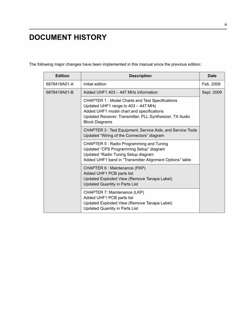
DOCUMENT HISTORY
The following major changes have been implemented in this manual since the previous edition:
Edition Description Date
6878419A01-A Initial edition Feb. 2009
6878419A01-B Added UHF1 403 – 447 MHz information Sept. 2009
CHAPTER 1 : Model Charts and Test SpecificationsUpdated UHF1 range to 403 – 447 MHzAdded UHF1 model chart and specificationsUpdated Receiver, Transmitter, PLL Synthesizer, TX Audio Block Diagrams
CHAPTER 3 : Test Equipment, Service Aids, and Service ToolsUpdated “Wiring of the Connectors” diagram
CHAPTER 5 : Radio Programming and TuningUpdated “CPS Programming Setup” diagramUpdated “Radio Tuning Setup diagramAdded UHF1 band in “Transmitter Alignment Options” table
CHAPTER 6 : Maintenance (FKP)Added UHF1 PCB parts listUpdated Exploded View (Remove Tanapa Label)Updated Quantity in Parts List
CHAPTER 7: Maintenance (LKP)Added UHF1 PCB parts listUpdated Exploded View (Remove Tanapa Label)Updated Quantity in Parts List

iv
Notes
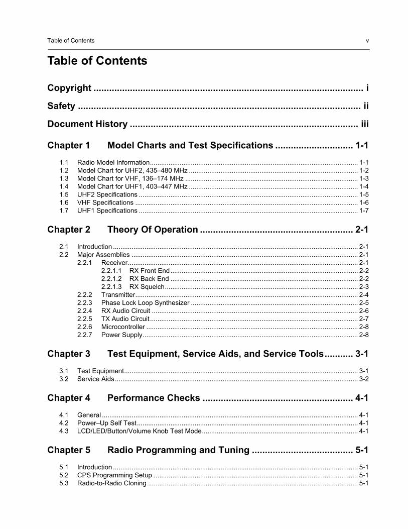
Table of Contents v
Table of Contents
Copyright ........................................................................................................ i
Safety ............................................................................................................. ii
Document History ........................................................................................ iii
Chapter 1 Model Charts and Test Specifications .............................. 1-1
1.1 Radio Model Information................................................................................................................ 1-11.2 Model Chart for UHF2, 435–480 MHz ........................................................................................... 1-21.3 Model Chart for VHF, 136–174 MHz ............................................................................................. 1-31.4 Model Chart for UHF1, 403–447 MHz ........................................................................................... 1-41.5 UHF2 Specifications ...................................................................................................................... 1-51.6 VHF Specifications ........................................................................................................................ 1-61.7 UHF1 Specifications ...................................................................................................................... 1-7
Chapter 2 Theory Of Operation ........................................................... 2-1
2.1 Introduction .................................................................................................................................... 2-12.2 Major Assemblies .......................................................................................................................... 2-1
2.2.1 Receiver............................................................................................................................ 2-12.2.1.1 RX Front End..................................................................................................... 2-22.2.1.2 RX Back End ..................................................................................................... 2-22.2.1.3 RX Squelch........................................................................................................ 2-3
2.2.2 Transmitter........................................................................................................................ 2-42.2.3 Phase Lock Loop Synthesizer .......................................................................................... 2-52.2.4 RX Audio Circuit ............................................................................................................... 2-62.2.5 TX Audio Circuit ................................................................................................................ 2-72.2.6 Microcontroller .................................................................................................................. 2-82.2.7 Power Supply.................................................................................................................... 2-8
Chapter 3 Test Equipment, Service Aids, and Service Tools........... 3-1
3.1 Test Equipment.............................................................................................................................. 3-13.2 Service Aids................................................................................................................................... 3-2
Chapter 4 Performance Checks .......................................................... 4-1
4.1 General .......................................................................................................................................... 4-14.2 Power–Up Self Test....................................................................................................................... 4-14.3 LCD/LED/Button/Volume Knob Test Mode.................................................................................... 4-1
Chapter 5 Radio Programming and Tuning ....................................... 5-1
5.1 Introduction .................................................................................................................................... 5-15.2 CPS Programming Setup .............................................................................................................. 5-15.3 Radio-to-Radio Cloning ................................................................................................................. 5-1
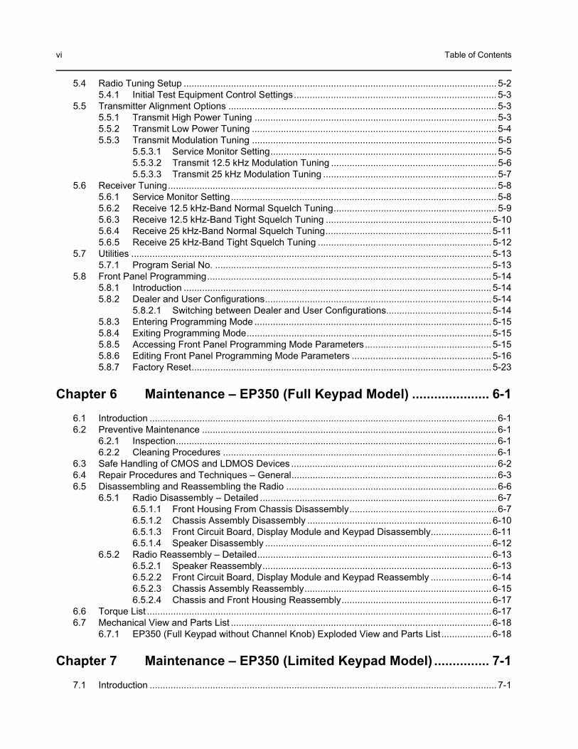
vi Table of Contents
5.4 Radio Tuning Setup ....................................................................................................................... 5-25.4.1 Initial Test Equipment Control Settings............................................................................. 5-3
5.5 Transmitter Alignment Options ...................................................................................................... 5-35.5.1 Transmit High Power Tuning ............................................................................................ 5-35.5.2 Transmit Low Power Tuning ............................................................................................. 5-45.5.3 Transmit Modulation Tuning ............................................................................................. 5-5
5.5.3.1 Service Monitor Setting...................................................................................... 5-55.5.3.2 Transmit 12.5 kHz Modulation Tuning ............................................................... 5-65.5.3.3 Transmit 25 kHz Modulation Tuning .................................................................. 5-7
5.6 Receiver Tuning............................................................................................................................. 5-85.6.1 Service Monitor Setting..................................................................................................... 5-85.6.2 Receive 12.5 kHz-Band Normal Squelch Tuning.............................................................. 5-95.6.3 Receive 12.5 kHz-Band Tight Squelch Tuning ............................................................... 5-105.6.4 Receive 25 kHz-Band Normal Squelch Tuning............................................................... 5-115.6.5 Receive 25 kHz-Band Tight Squelch Tuning .................................................................. 5-12
5.7 Utilities ......................................................................................................................................... 5-135.7.1 Program Serial No. ......................................................................................................... 5-13
5.8 Front Panel Programming............................................................................................................ 5-145.8.1 Introduction ..................................................................................................................... 5-145.8.2 Dealer and User Configurations...................................................................................... 5-14
5.8.2.1 Switching between Dealer and User Configurations........................................ 5-145.8.3 Entering Programming Mode .......................................................................................... 5-155.8.4 Exiting Programming Mode............................................................................................. 5-155.8.5 Accessing Front Panel Programming Mode Parameters................................................ 5-155.8.6 Editing Front Panel Programming Mode Parameters ..................................................... 5-165.8.7 Factory Reset.................................................................................................................. 5-23
Chapter 6 Maintenance – EP350 (Full Keypad Model) ..................... 6-1
6.1 Introduction .................................................................................................................................... 6-16.2 Preventive Maintenance ................................................................................................................ 6-1
6.2.1 Inspection.......................................................................................................................... 6-16.2.2 Cleaning Procedures ........................................................................................................ 6-1
6.3 Safe Handling of CMOS and LDMOS Devices .............................................................................. 6-26.4 Repair Procedures and Techniques – General.............................................................................. 6-36.5 Disassembling and Reassembling the Radio ................................................................................ 6-6
6.5.1 Radio Disassembly – Detailed .......................................................................................... 6-76.5.1.1 Front Housing From Chassis Disassembly........................................................ 6-76.5.1.2 Chassis Assembly Disassembly ...................................................................... 6-106.5.1.3 Front Circuit Board, Display Module and Keypad Disassembly....................... 6-116.5.1.4 Speaker Disassembly ...................................................................................... 6-12
6.5.2 Radio Reassembly – Detailed......................................................................................... 6-136.5.2.1 Speaker Reassembly....................................................................................... 6-136.5.2.2 Front Circuit Board, Display Module and Keypad Reassembly ....................... 6-146.5.2.3 Chassis Assembly Reassembly....................................................................... 6-156.5.2.4 Chassis and Front Housing Reassembly......................................................... 6-17
6.6 Torque List ................................................................................................................................... 6-176.7 Mechanical View and Parts List ................................................................................................... 6-18
6.7.1 EP350 (Full Keypad without Channel Knob) Exploded View and Parts List ................... 6-18
Chapter 7 Maintenance – EP350 (Limited Keypad Model) ............... 7-1
7.1 Introduction .................................................................................................................................... 7-1

Table of Contents vii
7.2 Preventive Maintenance ................................................................................................................ 7-17.2.1 Inspection ......................................................................................................................... 7-17.2.2 Cleaning Procedures ........................................................................................................ 7-1
7.3 Safe Handling of CMOS and LDMOS Devices.............................................................................. 7-27.4 Repair Procedures and Techniques – General ............................................................................. 7-37.5 Disassembling and Reassembling the Radio ................................................................................ 7-6
7.5.1 Radio Disassembly – Detailed.......................................................................................... 7-77.5.1.1 Front Housing From Chassis Disassembly........................................................ 7-77.5.1.2 Chassis Assembly Disassembly ...................................................................... 7-107.5.1.3 Front Circuit Board, Display Module and Keypad Disassembly ...................... 7-127.5.1.4 Speaker Disassembly ...................................................................................... 7-13
7.5.2 Radio Reassembly – Detailed ........................................................................................ 7-137.5.2.1 Speaker Reassembly....................................................................................... 7-137.5.2.2 Front Circuit Board, Display Module and Keypad Reassembly ....................... 7-147.5.2.3 Chassis Assembly Reassembly....................................................................... 7-157.5.2.4 Chassis and Front Housing Reassembly......................................................... 7-17
7.6 Torque List................................................................................................................................... 7-187.7 Mechanical View and Parts List................................................................................................... 7-18
7.7.1 EP350 (Limited Keypad without Channel Knob) Exploded View and Parts List ............. 7-18
Chapter 8 Troubleshooting Tables ..................................................... 8-1
8.1 Error Codes ................................................................................................................................... 8-18.2 Troubleshooting Table for Receiver............................................................................................... 8-28.3 Troubleshooting Table for Transmitter........................................................................................... 8-3
Appendix A Accessories .........................................................................A-1
Appendix B Warranty, Service Support, and Replacement Parts .......B-1
B.1 Scope of Manual............................................................................................................................B-1B.2 Warranty ........................................................................................................................................B-1
B.2.1 What This Warranty Covers And For How Long...............................................................B-1B.2.2 General Provisions ...........................................................................................................B-1B.2.3 How To Get Warranty Service ..........................................................................................B-2B.2.4 What This Warranty Does Not Cover ...............................................................................B-2B.2.5 Patent And Software Provisions .......................................................................................B-3B.2.6 Piece Parts .......................................................................................................................B-4
B.2.6.1 Basic Ordering ...................................................................................................B-4B.2.6.2 Motorola Online .................................................................................................B-4
B.2.7 Motorola Service Centers .................................................................................................B-4Glossary of Terms .....................................................................................G-1
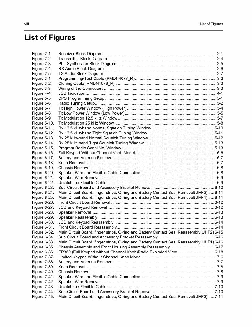
viii List of Figures
List of Figures
Figure 2-1. Receiver Block Diagram................................................................................................... 2-1Figure 2-2. Transmitter Block Diagram............................................................................................... 2-4Figure 2-3. PLL Synthesizer Block Diagram....................................................................................... 2-5Figure 2-4. RX Audio Block Diagram.................................................................................................. 2-6Figure 2-5. TX Audio Block Diagram .................................................................................................. 2-7Figure 3-1. Programming/Test Cable (PMDN4077_R) ....................................................................... 3-3Figure 3-2. Cloning Cable (PMDN4076_R) ........................................................................................ 3-3Figure 3-3. Wiring of the Connectors .................................................................................................. 3-3Figure 4-4. LCD Indication .................................................................................................................. 4-1Figure 5-5. CPS Programming Setup ................................................................................................. 5-1Figure 5-6. Radio Tuning Setup.......................................................................................................... 5-2Figure 5-7. Tx High Power Window (High Power) .............................................................................. 5-4Figure 5-8. Tx Low Power Window (Low Power)................................................................................ 5-5Figure 5-9. Tx Modulation 12.5 kHz Window ...................................................................................... 5-7Figure 5-10. Tx Modulation 25 kHz Window ......................................................................................... 5-8Figure 5-11. Rx 12.5 kHz-band Normal Squelch Tuning Window ...................................................... 5-10Figure 5-12. Rx 12.5 kHz-band Tight Squelch Tuning Window .......................................................... 5-11Figure 5-13. Rx 25 kHz-band Normal Squelch Tuning Window ......................................................... 5-12Figure 5-14. Rx 25 kHz-band Tight Squelch Tuning Window ............................................................. 5-13Figure 5-15. Program Radio Serial No. Window................................................................................. 5-13Figure 6-16. Full Keypad Without Channel Knob Model....................................................................... 6-6Figure 6-17. Battery and Antenna Removal.......................................................................................... 6-7Figure 6-18. Knob Removal .................................................................................................................. 6-7Figure 6-19. Chassis Removal.............................................................................................................. 6-8Figure 6-20. Speaker Wire and Flexible Cable Connection.................................................................. 6-8Figure 6-21. Speaker Wire Removal..................................................................................................... 6-9Figure 6-22. Unlatch the Flexible Cable................................................................................................ 6-9Figure 6-23. Sub-Circuit Board and Accessory Bracket Removal ...................................................... 6-10Figure 6-24. Main Circuit Board, finger strips, O-ring and Battery Contact Seal Removal(UHF2) ..... 6-11Figure 6-25. Main Circuit Board, finger strips, O-ring and Battery Contact Seal Removal(UHF1) ..... 6-11Figure 6-26. Front Circuit Board Removal .......................................................................................... 6-12Figure 6-27. LCD and Keypad Removal .............................................................................................6-12Figure 6-28. Speaker Removal ........................................................................................................... 6-13Figure 6-29. Speaker Reassembly ..................................................................................................... 6-13Figure 6-30. LCD and Keypad Reassembly ....................................................................................... 6-14Figure 6-31. Front Circuit Board Reassembly..................................................................................... 6-14Figure 6-32. Main Circuit Board, finger strips, O-ring and Battery Contact Seal Reassembly(UHF2) 6-15Figure 6-34. Sub Circuit Board and Accessory Bracket Reassembly................................................. 6-16Figure 6-33. Main Circuit Board, finger strips, O-ring and Battery Contact Seal Reassembly(UHF1) 6-16Figure 6-35. Chassis Assembly and Front Housing Assembly Reassembly ...................................... 6-17Figure 6-36. EP350 (Full Keypad without Channel Knob)Radio Exploded View ................................ 6-18Figure 7-37. Limited Keypad Without Channel Knob Model ................................................................. 7-6Figure 7-38. Battery and Antenna Removal.......................................................................................... 7-7Figure 7-39. Knob Removal .................................................................................................................. 7-8Figure 7-40. Chassis Removal.............................................................................................................. 7-8Figure 7-41. Speaker Wire and Flexible Cable Connection.................................................................. 7-9Figure 7-42. Speaker Wire Removal..................................................................................................... 7-9Figure 7-43. Unlatch the Flexible Cable.............................................................................................. 7-10Figure 7-44. Sub-Circuit Board and Accessory Bracket Removal ...................................................... 7-10Figure 7-45. Main Circuit Board, finger strips, O-ring and Battery Contact Seal Removal(UHF2) ..... 7-11
List of Figures ix
Figure 7-46. Main Circuit Board, finger strips, O-ring and Battery Contact Seal Removal (UHF1) .... 7-11Figure 7-47. Front Circuit Board Removal .......................................................................................... 7-12Figure 7-48. LCD and Keypad Removal............................................................................................. 7-12Figure 7-49. Speaker Removal........................................................................................................... 7-13Figure 7-50. Speaker Reassembly ..................................................................................................... 7-14Figure 7-51. LCD and Keypad Reassembly ....................................................................................... 7-14Figure 7-52. Front Circuit Board Reassembly .................................................................................... 7-15Figure 7-53. Main Circuit Board, O-ring and Battery Contact Seal Reassembly(UHF2) .................... 7-16Figure 7-54. Main Circuit Board, finger strips, O-ring and Battery Contact Seal Reassembly(UHF1) 7-16Figure 7-55. Sub Circuit Board and Accessory Bracket Reassembly................................................. 7-17Figure 7-56. Chassis Assembly and Front Housing Assembly Reassembly ...................................... 7-17Figure 7-57. EP350 (Limited Keypad without Channel Knob) – Exploded View ................................ 7-18
x List of Tables
List of Tables
Table 1-1. Radio Model Number (Example:MDH03RDH8AA7) ........................................................ 1-1Table 3-2. Recommended Test Equipment ....................................................................................... 3-1Table 3-3. Service Aids...................................................................................................................... 3-2Table 4-4. Radio Operation in Test Mode.......................................................................................... 4-1Table 5-5. Initial Equipment Control Settings .................................................................................... 5-3Table 5-6. Transmit High/Low Power Level....................................................................................... 5-3Table 5-7. Transmit Modulation Tuning ............................................................................................. 5-5Table 5-8. Receiver Squelch Tuning ................................................................................................. 5-8Table 5-9. Front Panel Programming Mode Parameters................................................................. 5-16Table 6-10. Lead Free Solder Wire Part Number List ......................................................................... 6-3Table 6-11. Lead Free Solder Paste Part Number List........................................................................ 6-3Table 6-12. Torque Chart .................................................................................................................. 6-17Table 6-13. Parts List (Full Keypad without Channel Knob) .............................................................. 6-19Table 7-14. Lead Free Solder Wire Part Number List ......................................................................... 7-4Table 7-15. Lead Free Solder Paste Part Number List........................................................................ 7-4Table 7-16. Torque Chart .................................................................................................................. 7-18Table 7-17. Parts List (Limited Keypad without Channel Knob) ........................................................ 7-19Table 8-18. Error Code Display ........................................................................................................... 8-1Table 8-19. Receiver Troubleshooting Table....................................................................................... 8-2Table 8-20. Transmitter Troubleshooting Table................................................................................... 8-3Table B-1. Portable Radios and Product Accessories Warranty........................................................B-1
Related PublicationsLACR
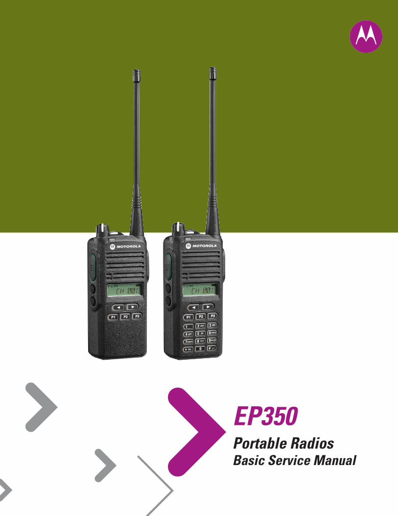
EP350 Series Radios User Guide(English, Latin American Spanish, Brazilian Portuguese)...............................................6878081A01
EP350 Series Radios Quick Reference Card(English, Latin American Spanish, Brazilian Portuguese)............................................. 68007024010
EP350 Basic Service Manual ..................................................................................................6878419A01EP350 Detailed Service Manual ..............................................................................................6878422A01Product Safety and RF Exposure Booklet ................................................................................6881095C98
Notations Used in This Manual xi
Notations Used in This ManualThroughout the text in this publication, you will notice the use of the following notations. These notations are used to emphasize that safety hazards exist, and due care must be taken and observed.
Note An operational procedure, practice, or condition that isessential to emphasize.
CAUTION indicates a potentially hazardous situation which, if not avoided, might result in equipment damage.

xii Summary of Bands Available
Summary of Bands AvailableTable below lists all the bands available in this manual. For details, please refer to the Model Charts section.
Frequency Band Bandwidth Power Level
UHF2 435–480 MHz 1W or 4W
VHF 136– 74 MHz 1W or 5W
UHF1 403–447 MHz 1W or 4W

Chapter 1 Model Charts and Test Specifications
1.1 Radio Model InformationThe model number and serial number are located on a label attached to the back of your radio. You can determine the RF output power, frequency band, protocols, and physical packages. The example below shows one portable radio model number and its specific characteristics.
Table 1-1. Radio Model Number (Example:MDH03RDH8AA7)
Regional Prefix
Type of Unit
Model Series Freq. Band Power
LevelPhysical Packages
Channel Spacing Protocol Feature
Level
LA H 03 RUHF
(435–480 MHz)
KVHF
(136–174 MHz)
M200MHz
(216–223 MHz)
N200MHz
(245–247 MHz)
E300MHz
(350–390 MHz)
QUHF
(403–447 MHz)
SUHF
(470–512 MHz)
D4 W
C2 W
E5 W
HLimited Keypad without
Channel Knob
KFull Keypad
without Channel
Knob
TFull Keypad RTTE Model
ULimited Keypad
RTTE Model
812.5/25k
412.5k
620/25k
912.5/20/
25k
AA 7No
Front Panel Prog. with
Scrambling
1Fixed Freq.
Tier 1
2Fixed Freq.
Tier 2
3Fixed Freq.
Tier 3
4Fixed Freq.
Tier 4
5Fixed Freq.
Tier 5
9Front Panel
Prog. with
Scrambling
LA =
LA
CR
H =
Por
tabl
e
03 =
CP
Fam
ily M
odel
Ser
ies
AA
= C
onve
ntio
nal

1-2 Model Charts and Test Specifications: Model Chart for UHF2, 435–480 MHz
1.2 Model Chart for UHF2, 435–480 MHz
EP350, UHF2, 435–480 MHz Model Description
LAH03RDK8AA9AN EP350 435 – 480M 4W 12.5/25K 99C Full Keypad
LAH03RDH8AA7AN EP350 435 – 480M 4W 12.5/25K 99C Limited Keypad
Item Description
X PMUE3148_ 435 – 480M 4W 12.5/25K 99C FKPFPP SCR
X PMUE3144_ 435 – 480M 4W 12.5/25K 99C LKP SCR
X PMDE4010_R 435 – 480M 4W PCB – PMUE3148_AL
X PMDE4012_R 435 – 480M 4W PCB – PMUE3144_AL
X PMDN4130_R Front Circuit Board, FKP
X PMDN4131_R Front Circuit Board, LKP
X X PMDN4129_R Sub Circuit Board, w/o Channel
X X 6878419A01 EP350 BASIC SERVICE MANUAL
X X 6878422A01 EP350 DETAILED SERVICE MANUAL
X = Indicates compatibility with model(s)
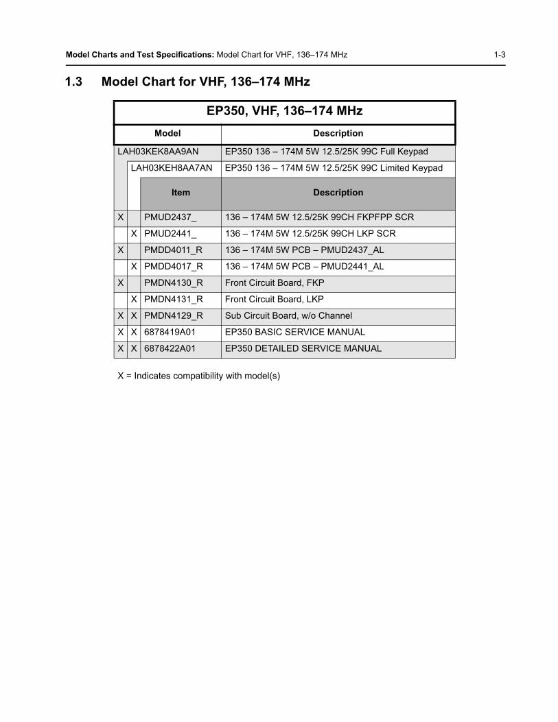
Model Charts and Test Specifications: Model Chart for VHF, 136–174 MHz 1-3
1.3 Model Chart for VHF, 136–174 MHz
EP350, VHF, 136–174 MHz Model Description
LAH03KEK8AA9AN EP350 136 – 174M 5W 12.5/25K 99C Full Keypad
LAH03KEH8AA7AN EP350 136 – 174M 5W 12.5/25K 99C Limited Keypad
Item Description
X PMUD2437_ 136 – 174M 5W 12.5/25K 99CH FKPFPP SCR
X PMUD2441_ 136 – 174M 5W 12.5/25K 99CH LKP SCR
X PMDD4011_R 136 – 174M 5W PCB – PMUD2437_AL
X PMDD4017_R 136 – 174M 5W PCB – PMUD2441_AL
X PMDN4130_R Front Circuit Board, FKP
X PMDN4131_R Front Circuit Board, LKP
X X PMDN4129_R Sub Circuit Board, w/o Channel
X X 6878419A01 EP350 BASIC SERVICE MANUAL
X X 6878422A01 EP350 DETAILED SERVICE MANUAL
X = Indicates compatibility with model(s)
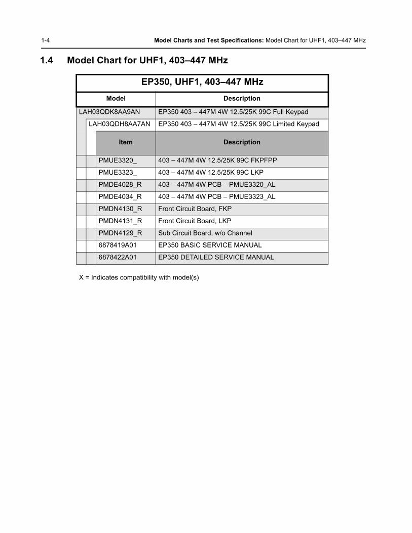
1-4 Model Charts and Test Specifications: Model Chart for UHF1, 403–447 MHz
1.4 Model Chart for UHF1, 403–447 MHz
EP350, UHF1, 403–447 MHz Model Description
LAH03QDK8AA9AN EP350 403 – 447M 4W 12.5/25K 99C Full Keypad
LAH03QDH8AA7AN EP350 403 – 447M 4W 12.5/25K 99C Limited Keypad
Item Description
PMUE3320_ 403 – 447M 4W 12.5/25K 99C FKPFPP
PMUE3323_ 403 – 447M 4W 12.5/25K 99C LKP
PMDE4028_R 403 – 447M 4W PCB – PMUE3320_AL
PMDE4034_R 403 – 447M 4W PCB – PMUE3323_AL
PMDN4130_R Front Circuit Board, FKP
PMDN4131_R Front Circuit Board, LKP
PMDN4129_R Sub Circuit Board, w/o Channel
6878419A01 EP350 BASIC SERVICE MANUAL
6878422A01 EP350 DETAILED SERVICE MANUAL
X = Indicates compatibility with model(s)
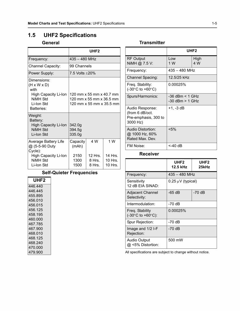
Model Charts and Test Specifications: UHF2 Specifications 1-5
1.5 UHF2 SpecificationsGeneral
Self-Quieter Frequencies
Transmitter
Receiver
All specifications are subject to change without notice.
UHF2
Frequency: 435 – 480 MHz
Channel Capacity: 99 Channels
Power Supply: 7.5 Volts ±20%
Dimensions:(H x W x D)withHigh Capacity Li-Ion NiMH StdLi-Ion Std
Batteries:
120 mm x 55 mm x 40.7 mm 120 mm x 55 mm x 36.5 mm 120 mm x 55 mm x 35.5 mm
Weight: Battery:
High Capacity Li-IonNiMH StdLi-Ion Std
342.0g394.5g 335.0g
Average Battery Life @ (5-5-90 DutyCycle):
High Capacity Li-IonNiMH StdLi-Ion Std
Capacity(mAh)
215013001500
4 W
12 Hrs.8 Hrs.8 Hrs.
1 W
14 Hrs.10 Hrs.10 Hrs.
UHF2446.440446.445455.895456.010456.015456.125458.195460.000467.785467.900468.010468.125468.240470.000479.900
UHF2
RF OutputNiMH @ 7.5 V:
Low1 W
High4 W
Frequency: 435 – 480 MHz
Channel Spacing: 12.5/25 kHz
Freq. Stability:(-30°C to +60°C)
0.00025%
Spurs/Harmonics: -36 dBm < 1 GHz-30 dBm > 1 GHz
Audio Response:(from 6 dB/oct. Pre-emphasis, 300 to 3000 Hz)
+1, -3 dB
Audio Distortion:@ 1000 Hz, 60%Rated Max. Dev.
<5%
FM Noise: <-40 dB
UHF212.5 kHz
UHF225kHz
Frequency: 435 – 480 MHz
Sensitivity12 dB EIA SINAD:
0.25 μV (typical)
Adjacent Channel Selectivity:
-65 dB -70 dB
Intermodulation: -70 dB
Freq. Stability(-30°C to +60°C):
0.00025%
Spur Rejection: -70 dB
Image and 1/2 I-F Rejection:
-70 dB
Audio Output@ <5% Distortion:
500 mW
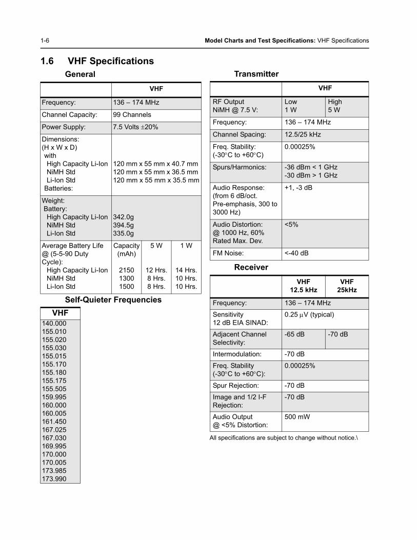
1-6 Model Charts and Test Specifications: VHF Specifications
1.6 VHF SpecificationsGeneral
Self-Quieter Frequencies
Transmitter
Receiver
All specifications are subject to change without notice.\
VHF
Frequency: 136 – 174 MHz
Channel Capacity: 99 Channels
Power Supply: 7.5 Volts ±20%
Dimensions:(H x W x D)withHigh Capacity Li-Ion NiMH StdLi-Ion Std
Batteries:
120 mm x 55 mm x 40.7 mm 120 mm x 55 mm x 36.5 mm 120 mm x 55 mm x 35.5 mm
Weight: Battery:
High Capacity Li-IonNiMH StdLi-Ion Std
342.0g394.5g 335.0g
Average Battery Life @ (5-5-90 DutyCycle):
High Capacity Li-IonNiMH StdLi-Ion Std
Capacity(mAh)
215013001500
5 W
12 Hrs.8 Hrs.8 Hrs.
1 W
14 Hrs.10 Hrs.10 Hrs.
VHF140.000155.010155.020155.030155.015155.170155.180155.175155.505159.995160.000160.005161.450167.025167.030169.995170.000170.005173.985173.990
VHF
RF OutputNiMH @ 7.5 V:
Low1 W
High5 W
Frequency: 136 – 174 MHz
Channel Spacing: 12.5/25 kHz
Freq. Stability:(-30°C to +60°C)
0.00025%
Spurs/Harmonics: -36 dBm < 1 GHz-30 dBm > 1 GHz
Audio Response:(from 6 dB/oct. Pre-emphasis, 300 to 3000 Hz)
+1, -3 dB
Audio Distortion:@ 1000 Hz, 60%Rated Max. Dev.
<5%
FM Noise: <-40 dB
VHF12.5 kHz
VHF 25kHz
Frequency: 136 – 174 MHz
Sensitivity12 dB EIA SINAD:
0.25 μV (typical)
Adjacent Channel Selectivity:
-65 dB -70 dB
Intermodulation: -70 dB
Freq. Stability(-30°C to +60°C):
0.00025%
Spur Rejection: -70 dB
Image and 1/2 I-F Rejection:
-70 dB
Audio Output@ <5% Distortion:
500 mW
Model Charts and Test Specifications: UHF1 Specifications 1-7
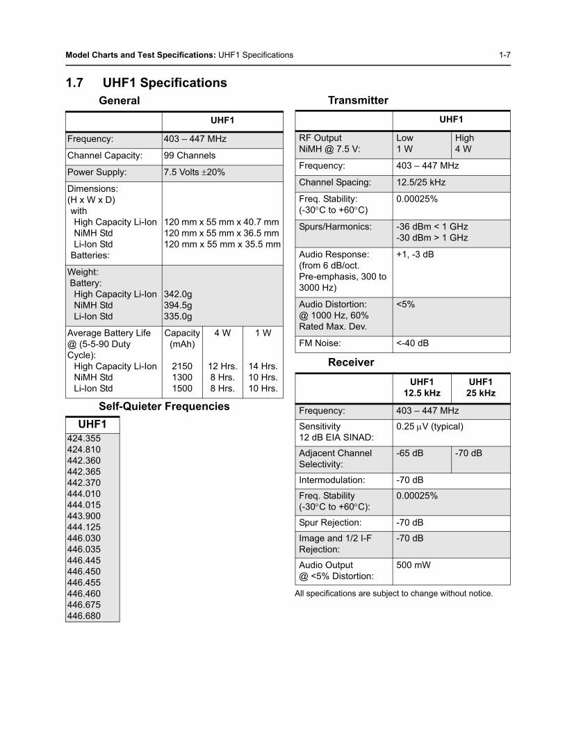
1.7 UHF1 SpecificationsGeneral
Self-Quieter Frequencies
Transmitter
Receiver
All specifications are subject to change without notice.
UHF1
Frequency: 403 – 447 MHz
Channel Capacity: 99 Channels
Power Supply: 7.5 Volts ±20%
Dimensions:(H x W x D)withHigh Capacity Li-Ion NiMH StdLi-Ion Std
Batteries:
120 mm x 55 mm x 40.7 mm 120 mm x 55 mm x 36.5 mm 120 mm x 55 mm x 35.5 mm
Weight: Battery:
High Capacity Li-IonNiMH StdLi-Ion Std
342.0g394.5g 335.0g
Average Battery Life @ (5-5-90 DutyCycle):
High Capacity Li-IonNiMH StdLi-Ion Std
Capacity(mAh)
215013001500
4 W
12 Hrs.8 Hrs.8 Hrs.
1 W
14 Hrs.10 Hrs.10 Hrs.
UHF1424.355424.810442.360442.365442.370444.010444.015443.900444.125446.030446.035446.445446.450446.455446.460446.675446.680
UHF1
RF OutputNiMH @ 7.5 V:
Low1 W
High4 W
Frequency: 403 – 447 MHz
Channel Spacing: 12.5/25 kHz
Freq. Stability:(-30°C to +60°C)
0.00025%
Spurs/Harmonics: -36 dBm < 1 GHz-30 dBm > 1 GHz
Audio Response:(from 6 dB/oct. Pre-emphasis, 300 to 3000 Hz)
+1, -3 dB
Audio Distortion:@ 1000 Hz, 60%Rated Max. Dev.
<5%
FM Noise: <-40 dB
UHF112.5 kHz
UHF125 kHz
Frequency: 403 – 447 MHz
Sensitivity12 dB EIA SINAD:
0.25 μV (typical)
Adjacent Channel Selectivity:
-65 dB -70 dB
Intermodulation: -70 dB
Freq. Stability(-30°C to +60°C):
0.00025%
Spur Rejection: -70 dB
Image and 1/2 I-F Rejection:
-70 dB
Audio Output@ <5% Distortion:
500 mW

1-8 Model Charts and Test Specifications: UHF1 Specifications
Notes
Chapter 2 Theory Of Operation
2.1 IntroductionThis chapter provides a basic theory of operation for the radio components.
2.2 Major Assemblies• Main PCB – Contains the RF circuits which comprises receiver, transmitter, phase-locked loop
(PLL) frequency synthesizer, micro controller, power supply, audio and digital circuits• Display and Keypad PCB (Limited and Full Keypad models only) – 8 characters (14 segments
star burst) and 10 icons with backlighting, liquid-crystal display (LCD)• Volume Knob PCB (PMDN4129AR) – Rotary Volume Knob
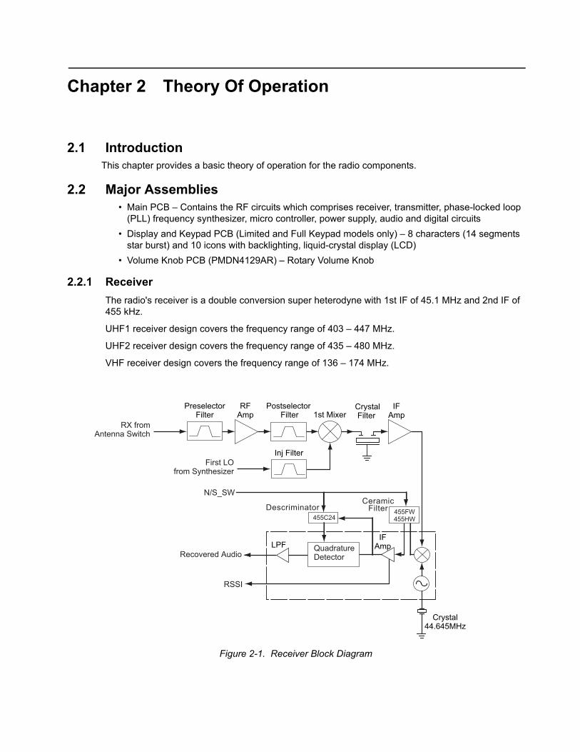
2.2.1 ReceiverThe radio's receiver is a double conversion super heterodyne with 1st IF of 45.1 MHz and 2nd IF of 455 kHz.
UHF1 receiver design covers the frequency range of 403 – 447 MHz.
UHF2 receiver design covers the frequency range of 435 – 480 MHz.
VHF receiver design covers the frequency range of 136 – 174 MHz.
Figure 2-1. Receiver Block Diagram
CrystalFilter
Crystal44.645MHz
1st MixerRF
AmpPreselector
FilterPostselector
Filter
RX fromAntenna Switch
Inj Filter
First LOfrom Synthesizer
IFAmp
IFAmpLPF
CeramicFilterDescriminator
455FW455HW
QuadratureDetector
RSSI
N/S_SW
Recovered Audio
455C24
2-2 Theory Of Operation: Major Assemblies
2.2.1.1 RX Front EndUHF1 : Receiver Front-end consists of a low pass filter, a pre-selector filter, a low noise RF Amplifier and a Post-selector filter. Incoming RF signal from the antenna is applied through the Harmonics Low Pass Filter (L409, L410, L411, C426, C427, C428, C429, C445, C446) and passes through the transmit/receive switch (CR301) and a varactor-tuned 2-pole pre-selector filter (L320, L324, C351, C361, CR314 and CR307) before routed to an RF amplifier (Q301). The pre-selector filter is an 8 step Band-shift filter, and the frequency shifting is controlled by varactor diodes (CR314 and CR307) connected to the CPU. The filter output is coupled to a 13 dB RF amplifier Q301 which outputs the RF signal to the post-selector filter (L323, L328, C379, and C355) which is also a band shift filter configured to provide steeper low-side attenuation. The 2 varactor diodes (CR313 and CR305) with 8 frequency steps are also controlled by the CPU.
UHF2 : Receiver Front-end consists of a low pass filter, a pre-selector filter, a low noise RF Amplifier and a Post-selector filter. Incoming RF signal from the antenna is applied through the Harmonics Low Pass Filter (L409, L410, L411, C426, C427, C428, C429, C445, C446) and passes through the transmit/receive switch (CR301) and a varactor-tuned 2-pole pre-selector filter (L320, L324, C351, C361, CR314 and CR307) before routed to an RF amplifier (Q301). The pre-selector filter is an 8 step Band-shift filter, and the frequency shifting is controlled by varactor diodes (CR314 and CR307) connected to the CPU. The filter output is coupled to a 13 dB RF amplifier Q301 which outputs the RF signal to the post-selector filter (L323, L322, L328, C379, C354 and C355) which is also a band shift filter configured to provide steeper low-side attenuation. The 3 varactor diodes (CR313, CR304 and CR305) with 8 frequency steps are also controlled by the CPU.
VHF : Receiver Front-end consists of a low pass filter, a pre-selector filter, a low noise RF Amplifier, a Post-selector filter. Incoming RF signal from antenna is applied through the Harmonics Low Pass Filter (L409, L410, L411, C426, C427, C428, C429, C430, C445, C446) and passes the transmit/receive switch (CR301) and a varactor-tuned 2-pole pre-selector filter (L301, L302, L303, L304, C301, CR302, CR303, C304, C305, C307, C308) before routed to an RF amplifier (Q301). The pre-selector filter is a 6 step Band-shift filter, and the frequency shifting is controlled by varactor diodes (CR302 & CR303) connected to the CPU. The filter output is coupled to a 13 dB RF amplifier Q301 which outputs the RF signal to the post-selector filter (L308, L309, L311, C315 and C354) which is also a band shift filter configured to provide steeper low-side attenuation. The 2 units of 6 step frequency varactor diodes (CR305, CR307) are also controlled by the CPU.
2.2.1.2 RX Back EndUHF1 : RF signal from RX front-end is then directed to a Double Balanced Mixer (L329, L333 and CR316). 1st LO signal from VCO is filtered by an injection filter (L310, L331, C325, C326 and C387) to remove harmonics.
After passing through a pair of 45.1 MHz Crystal filter, the 1st IF signal is amplified by 15 dB via an IF amp (Q303) and channeled to IF IC (U201) to be mixed thus producing the 2nd IF Frequency (455 kHz):
1st IF (45.1 MHz) - 2nd LO (44.645 MHz) = 2nd IF (455 kHz)
Depending on channel spacing, the 2nd IF frequency passes through the wide (CF1) and/or narrow (CF2) filters to eliminate undesired signals before being finally demodulated by demodulator in U201 with Recovered Audio as the final output.
Theory Of Operation: Major Assemblies 2-3
UHF2 : RF signal from RX front-end is then directed to a Single Balanced Mixer (L329, L333, Q306, and Q307). 1st LO signal from VCO is filtered by an injection filter (L310, L331, C325, C326, C327) to remove harmonics.
After passing through a pair of 45.1 MHz Crystal filter, the 1st IF signal is amplified by 15 dB via an IF amp (Q303) and channeled to IF IC (U201) to be mixed thus producing the 2nd IF Frequency (455 kHz):
1st IF (45.1 MHz) - 2nd LO (44.645 MHz) = 2nd IF (455 kHz)
Depending on channel spacing, the 2nd IF frequency passes through the wide (CF1) and/or narrow (CF2) filters to eliminate undesired signals before being finally demodulated by demodulator in U201 with Recovered Audio as the final output.
VHF : RF signal from RX front-end is then directed to a Single Balanced Mixer (L329, L333, Q306, and Q307). 1st LO signal from VCO is filtered by an injection filter (L310, L331, C325, C326 and C333) to remove harmonics.
After passing through a pair of 45.1 MHz Crystal filter, The 1st IF signal is amplified by 15 dB via an IF amp (Q303) and channeled to IF IC (U201) to be mixed thus producing 2nd IF Frequency (455 kHz)
1st IF (45.1 MHz) - 2nd LO (44.645 MHz) = 2nd IF (455 kHz)
Depending on channel spacing, the 2nd IF frequency passes through wide (CF1) or narrow (CF2) filter to eliminate undesired signals before being finally demodulated by demodulator in U201 with Recovered Audio as the final output.
2.2.1.3 RX SquelchThe mute (squelch) circuitry switches off the audio amplifier when no audio is detected from the recovered audio. The squelch circuit main components are U202 & U201.
U202 will adjust the squelch circuit sensitivity depending on Noise level from recovered audio. Noise level is amplified by internal amplifier of U201 to help U202 decide the squelch circuit sensitivity. If the noise level is over the set threshold, the microprocessor mutes the radio.
Note Perform squelch tuning after any RX part replacement. Refer Chapter 5.6: Receiver Tuningon page 5-8.
2-4 Theory Of Operation: Major Assemblies
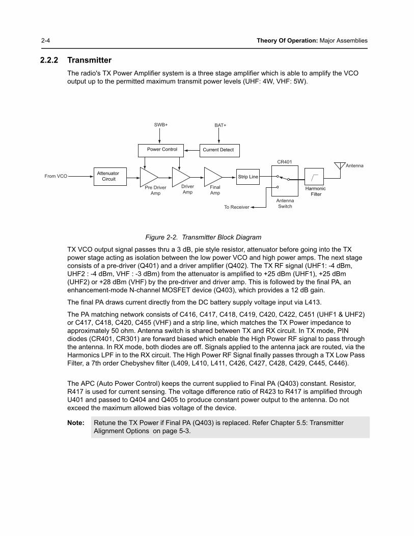
2.2.2 TransmitterThe radio's TX Power Amplifier system is a three stage amplifier which is able to amplify the VCO output up to the permitted maximum transmit power levels (UHF: 4W, VHF: 5W).
TX VCO output signal passes thru a 3 dB, pie style resistor, attenuator before going into the TX power stage acting as isolation between the low power VCO and high power amps. The next stage consists of a pre-driver (Q401) and a driver amplifier (Q402). The TX RF signal (UHF1: -4 dBm, UHF2 : -4 dBm, VHF : -3 dBm) from the attenuator is amplified to +25 dBm (UHF1), +25 dBm (UHF2) or +28 dBm (VHF) by the pre-driver and driver amp. This is followed by the final PA, an enhancement-mode N-channel MOSFET device (Q403), which provides a 12 dB gain.
The final PA draws current directly from the DC battery supply voltage input via L413.
The PA matching network consists of C416, C417, C418, C419, C420, C422, C451 (UHF1 & UHF2) or C417, C418, C420, C455 (VHF) and a strip line, which matches the TX Power impedance to approximately 50 ohm. Antenna switch is shared between TX and RX circuit. In TX mode, PIN diodes (CR401, CR301) are forward biased which enable the High Power RF signal to pass through the antenna. In RX mode, both diodes are off. Signals applied to the antenna jack are routed, via the Harmonics LPF in to the RX circuit. The High Power RF Signal finally passes through a TX Low Pass Filter, a 7th order Chebyshev filter (L409, L410, L411, C426, C427, C428, C429, C445, C446).
The APC (Auto Power Control) keeps the current supplied to Final PA (Q403) constant. Resistor, R417 is used for current sensing. The voltage difference ratio of R423 to R417 is amplified through U401 and passed to Q404 and Q405 to produce constant power output to the antenna. Do not exceed the maximum allowed bias voltage of the device.
Figure 2-2. Transmitter Block Diagram
Note: Retune the TX Power if Final PA (Q403) is replaced. Refer Chapter 5.5: Transmitter Alignment Options on page 5-3.
Attenuator
Circuit
Pre Driver
Amp
From VCO
Driver
AmpFinal
Amp
Power Control
Strip Line
Current Detect
SWB+ BAT+
Antenna
SwitchTo Receiver
CR401
Harmonic
Filter
Antenna

Theory Of Operation: Major Assemblies 2-5
2.2.3 Phase Lock Loop SynthesizerThe Phase Lock Loop (PLL) synthesizer subsystem consists of the reference oscillator (VCTCXO), VCO, PLL IC, Charge pump and Loop filter.
VCTCXO (Voltage Controlled Temperature Compensated crystal Oscillator) reference frequency (12.8 MHz) provides reference to PLL IC, with stability of +/-2.5PPM at -30° to +60°C. This reference frequency is divided to 6.25 kHz or 5 kHz by PLL IC. PLL IC outputs 2 Signals (P & R) depending on phase difference. A charge pump is used to charge these output signals from 0 – 3.3 V up to 0 – 10 V which is required to control the VCO. A voltage doubler (U507) converts 5 V to 10 V to supply the necessary voltage for a higher frequency resolution in VCO. The Loop filter is a Low Pass filter (C751 – C754, R726 – R728) to reduce the residual side-band noise of VCO Reference Frequency for the best signal-to-noise ratio. The VCO module contains both RX VCO and TX VCO, configured as Collpits oscillators and connects to DC power through cascaded buffers. Q705 and Q305 enable RX VCO when RX_EN is high. Q706 and Q503 enable TX VCO when TX_EN1 is high.
The input audio signal for TX VCO is from (U501-B) and applied to a varactor diodes (CR703) in TX VCO to be modulated into TX RF signal.
Figure 2-3. PLL Synthesizer Block Diagram
Modulating
Signal
FL701
12.8MHz
Ref.OSC.
Charge
Pump
Loop
Filter
TX VCO
RX OutTo Mixer
To PA DriverTX Out
Circuit
RX VCO
Circuit
Voltage
Doubler
Synthesizer
U701
PLL Data
from μP

2-6 Theory Of Operation: Major Assemblies
2.2.4 RX Audio CircuitThe RX audio circuit consists of Audio Processor IC, Audio amp, speakers & Sub-tone system.
The RX Audio from U201 is channeled to Audio processor IC. VR3 controls the received demodulated signal level from -4.0 dB to +3.5 dB in 0.5 dB steps. RX LPF eliminates high-frequency audio components > 3 kHz. TX/RX HPF eliminates low-frequency audio components lower < 250Hz. Descrambler (if ON) inverts the spectrum distribution of audio signals with respect to scrambling frequency. De-emphasis (if ON) restores high-frequency component of audio signal which has been emphasized by the pre-emphasis circuit in transmitting radio. Expander (if ON) expands audio signal by 0.5 dB to restore the original signal compressed by transmitting radio. VR4 amplifies RX audio level by -18.0 dB, with -4.5 dB to +4.5 dB in 0.25 dB steps adjustment range. Smoothing filter (SMF) eliminates high-frequency and clock components, generated by ASIC.
Sub-audio Programmable LPF totally eliminates voice audio from Audio signal to extract sub-audio tone. VR5 regulates the output level of extracted sub-audio tone and sends it to a high pass filter (U105-A,B) with 4 selectable cut-off frequencies and finally passes through a comparator (U105-C), to square the signal and sends it to the MCU.
The output audio signal of Audio Processor IC is directed to volume control switch (SW/VOL1) which is controlled by user and is finally amplified by U601BTL Audio Amplifier to a sufficient level to drive either the external or internal speaker.
Figure 2-4. RX Audio Block Diagram
VR3Scrambler /
Descrambler
De-
emphasisExpander VR4 SMF
SVR
IN-
IN+
OUT-
OUT+
Audio Mute
control
RX LPF TX/RX HPFRXA1
-4 to +3.5dB /
0.5dB -18, -4.5 to + 4.5dB /
0.25dB
Audio Processor IC (AK2347)
Audio IN
(from IF IC)
VR5
Sub audio
Programmable
LPF
To CPU
(tone detect)
pin 24
pin 18
pin 21
Audio Amp.
U102
U601
Vol1
-6 to +6dB /
0.5dB
INT SPK.
EXT SPK.
J601
Sub audio
HPFU105-A,B
Compar
ator
U105-C
Theory Of Operation: Major Assemblies 2-7
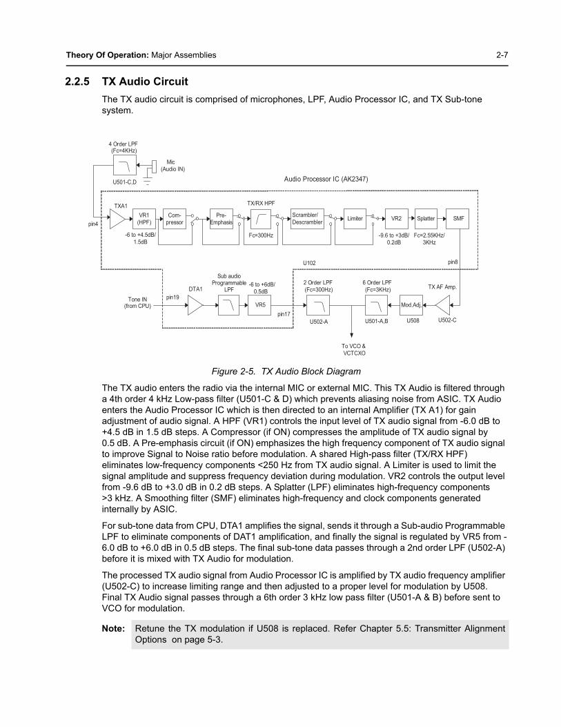
2.2.5 TX Audio CircuitThe TX audio circuit is comprised of microphones, LPF, Audio Processor IC, and TX Sub-tone system.
The TX audio enters the radio via the internal MIC or external MIC. This TX Audio is filtered through a 4th order 4 kHz Low-pass filter (U501-C & D) which prevents aliasing noise from ASIC. TX Audio enters the Audio Processor IC which is then directed to an internal Amplifier (TX A1) for gain adjustment of audio signal. A HPF (VR1) controls the input level of TX audio signal from -6.0 dB to +4.5 dB in 1.5 dB steps. A Compressor (if ON) compresses the amplitude of TX audio signal by 0.5 dB. A Pre-emphasis circuit (if ON) emphasizes the high frequency component of TX audio signal to improve Signal to Noise ratio before modulation. A shared High-pass filter (TX/RX HPF) eliminates low-frequency components <250 Hz from TX audio signal. A Limiter is used to limit the signal amplitude and suppress frequency deviation during modulation. VR2 controls the output level from -9.6 dB to +3.0 dB in 0.2 dB steps. A Splatter (LPF) eliminates high-frequency components >3 kHz. A Smoothing filter (SMF) eliminates high-frequency and clock components generated internally by ASIC.
For sub-tone data from CPU, DTA1 amplifies the signal, sends it through a Sub-audio Programmable LPF to eliminate components of DAT1 amplification, and finally the signal is regulated by VR5 from -6.0 dB to +6.0 dB in 0.5 dB steps. The final sub-tone data passes through a 2nd order LPF (U502-A) before it is mixed with TX Audio for modulation.
The processed TX audio signal from Audio Processor IC is amplified by TX audio frequency amplifier (U502-C) to increase limiting range and then adjusted to a proper level for modulation by U508. Final TX Audio signal passes through a 6th order 3 kHz low pass filter (U501-A & B) before sent to VCO for modulation.
Figure 2-5. TX Audio Block Diagram
Note: Retune the TX modulation if U508 is replaced. Refer Chapter 5.5: Transmitter AlignmentOptions on page 5-3.
VR1
(HPF)Limiter
Scrambler/
DescramblerSplatter SMF
TX/RX HPFTXA1
-6 to +4.5dB/
1.5dB-9.6 to +3dB/
0.2dB
Audio Processor IC (AK2347)
Tone IN(from CPU) VR5
Sub audioProgrammable
LPF
pin4
pin17
pin8U102
-6 to +6dB/
0.5dB
Fc=300Hz
VR2Pre-
Emphasis
Com-
pressor
DTA1
pin19
To VCO &
VCTCXO
2 Order LPF
(Fc=300Hz)
U502-A
Mod.Adj,
6 Order LPF
(Fc=3KHz)
U501-A,B U508
TX AF Amp.
U502-C
4 Order LPF (Fc=4KHz)
U501-C,D
Mic
(Audio IN)
Fc=2.55KHz/
3KHz

2-8 Theory Of Operation: Major Assemblies
The output audio signal of Audio Processor IC is directed to volume control switch (SW/VOL1) controlled by user and is finally amplified by U601BTL Audio Amplifier to a sufficient level to drive either the external or internal speaker.
2.2.6 MicrocontrollerThe microprocessor or CPU includes Microprocessor (U101), EEPROM and support components. Radio operation is controlled by software in internal Flash ROM memory.
Radio parameters and customer specific information is stored in External EEPROM (U104). Pins 35 & 36 controls the Sub-PCB mounted LED indicators. PTT button (PB501) is linked to CPU via pin 44. Side programmable buttons 1 & 2 (PB502 & PB503) is linked via pin 21 & 32, respectively. Customer Programming Software (CPS) connects to the radio via a USB Programming cable (PMDN4077_R) through the microphone port (J601 pin 6) to pin 34 & 33 (PRG/CLONE_RX & PRG/CLONE_TX port). A 7.3728 MHz clock signal (X-in) is provided by FL101 to CPU. A voltage divider system (R153 & R154) is used by CPU to sense battery level.
2.2.7 Power SupplyThere are 4 voltage supplies in this radio: SWB+, 3.3 V, 5 V & 10 V.
SWB+ voltage is distributed to SW/Vol 1, Final PA (Q403 via R417) & APC circuit (U401).
The 3.3 V regulated supply (U506) is applied to CPU (U101), EEPROM (U104), DTMF IC (U103), Audio processor IC (U102), microphone biasing circuit and LCD/keypad driver.
The 5.0 V regulated source (U505) is distributed to RX back end circuit, RX/TX audio filters, 1/2 VCC generator, VCO (Q705, Q706), RX B+ (Q304), TXvB (Q407) & VCTCXO.
The 10.0 V regulated source (U507) is solely applied for Charge pump use.
Chapter 3 Test Equipment, Service Aids, and Service Tools
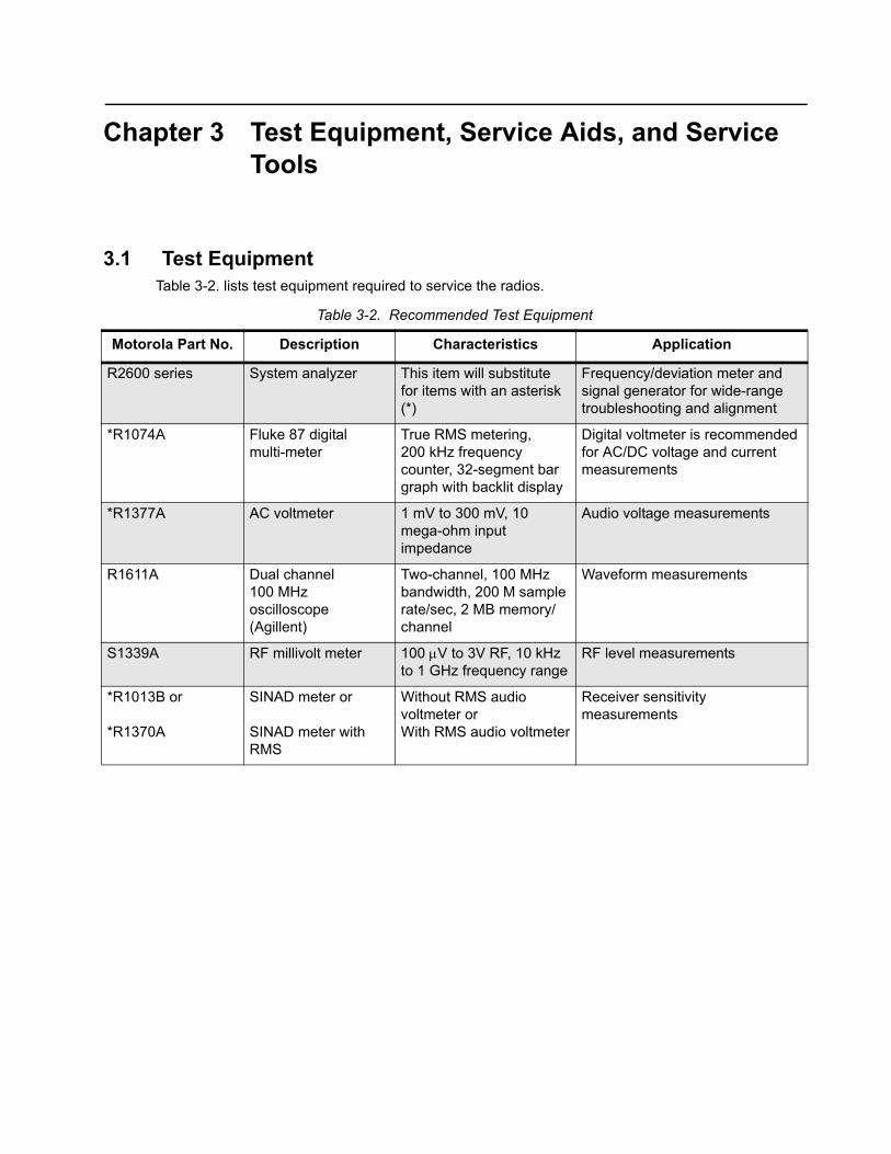
3.1 Test EquipmentTable 3-2. lists test equipment required to service the radios.
Table 3-2. Recommended Test Equipment
Motorola Part No. Description Characteristics Application
R2600 series System analyzer This item will substitute for items with an asterisk (*)
Frequency/deviation meter and signal generator for wide-range troubleshooting and alignment
*R1074A Fluke 87 digital multi-meter
True RMS metering, 200 kHz frequency counter, 32-segment bar graph with backlit display
Digital voltmeter is recommended for AC/DC voltage and current measurements
*R1377A AC voltmeter 1 mV to 300 mV, 10 mega-ohm input impedance
Audio voltage measurements
R1611A Dual channel 100 MHz oscilloscope (Agillent)
Two-channel, 100 MHz bandwidth, 200 M sample rate/sec, 2 MB memory/channel
Waveform measurements
S1339A RF millivolt meter 100 μV to 3V RF, 10 kHz to 1 GHz frequency range
RF level measurements
*R1013B or
*R1370A
SINAD meter or
SINAD meter with RMS
Without RMS audio voltmeter orWith RMS audio voltmeter
Receiver sensitivity measurements
3-2 Test Equipment, Service Aids, and Service Tools: Service Aids
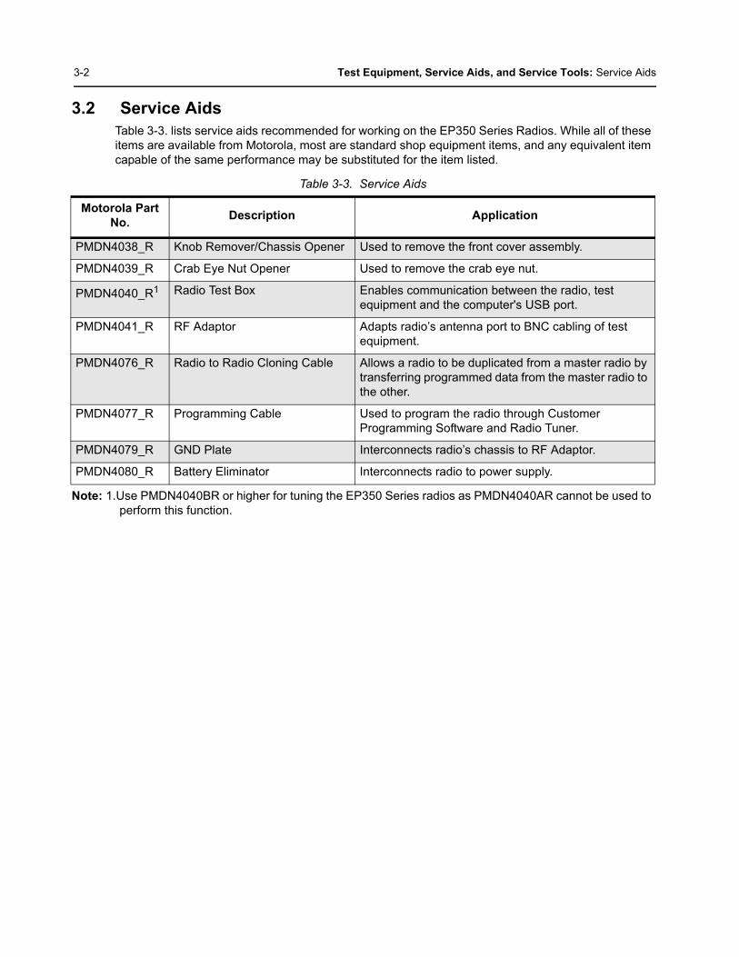
3.2 Service AidsTable 3-3. lists service aids recommended for working on the EP350 Series Radios. While all of these items are available from Motorola, most are standard shop equipment items, and any equivalent item capable of the same performance may be substituted for the item listed.
Note: 1.Use PMDN4040BR or higher for tuning the EP350 Series radios as PMDN4040AR cannot be used to perform this function.
Table 3-3. Service Aids
Motorola Part No. Description Application
PMDN4038_R Knob Remover/Chassis Opener Used to remove the front cover assembly.
PMDN4039_R Crab Eye Nut Opener Used to remove the crab eye nut.
PMDN4040_R1 Radio Test Box Enables communication between the radio, test equipment and the computer's USB port.
PMDN4041_R RF Adaptor Adapts radio’s antenna port to BNC cabling of test equipment.
PMDN4076_R Radio to Radio Cloning Cable Allows a radio to be duplicated from a master radio by transferring programmed data from the master radio to the other.
PMDN4077_R Programming Cable Used to program the radio through Customer Programming Software and Radio Tuner.
PMDN4079_R GND Plate Interconnects radio’s chassis to RF Adaptor.
PMDN4080_R Battery Eliminator Interconnects radio to power supply.
Test Equipment, Service Aids, and Service Tools: Service Aids 3-3
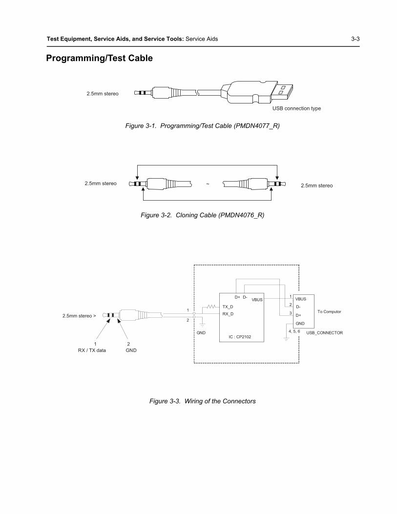
Programming/Test Cable
Figure 3-1. Programming/Test Cable (PMDN4077_R)
Figure 3-2. Cloning Cable (PMDN4076_R)
Figure 3-3. Wiring of the Connectors
2.5mm stereo
USB connection type
~ 2.5mm stereo 2.5mm stereo
2.5mm stereo >
1 2
TX_D
RX_D
4, 5, 6
GND
VBUS
D-
D+
D-D+VBUS
1
2
3
USB_CONNECTOR
2
1
GNDIC : CP2102
To Computor
RX / TX data GND

3-4 Test Equipment, Service Aids, and Service Tools: Service Aids
Notes

Chapter 4 Performance Checks
4.1 GeneralThese radios meet published specifications through their manufacturing process by utilizing high accuracy laboratory-quality test equipment. The recommended field service equipment is as accurate as the manufacturing equipment with few exceptions. This accuracy must be maintained in compliance with the manufacturer’s recommended calibration schedule.
4.2 Power–Up Self TestWhenever the radio is turn on, it initiates a self-test routine which checks the RAM, EEPROM hardware and EEPROM checksum. If Self Test passes, the green LED flashes once and a Self-Test Pass Tone is generated. If unsuccessful, the red LED flashes rapidly and a Self-Test Fail Tone is heard.
4.3 LCD/LED/Button/Volume Knob Test Mode1. Make sure the radio is turned off.
2. Turn on the radio and immediately press 3 times. The LED turns solid amber. The LCD displays the following indication (Figure 4-1) andthe backlight is activated.
3. The radio will operate as shown in Table 4-1 if any key is pressed while in test mode.
Figure 4-4. LCD Indication
Table 4-4. Radio Operation in Test Mode
Button LED LCD Indication Backlight Tone
, Right Solid Green • ON when button is pressed.
• OFF following button released (after a short period of inactivity).
, Left Solid Red – same as above –
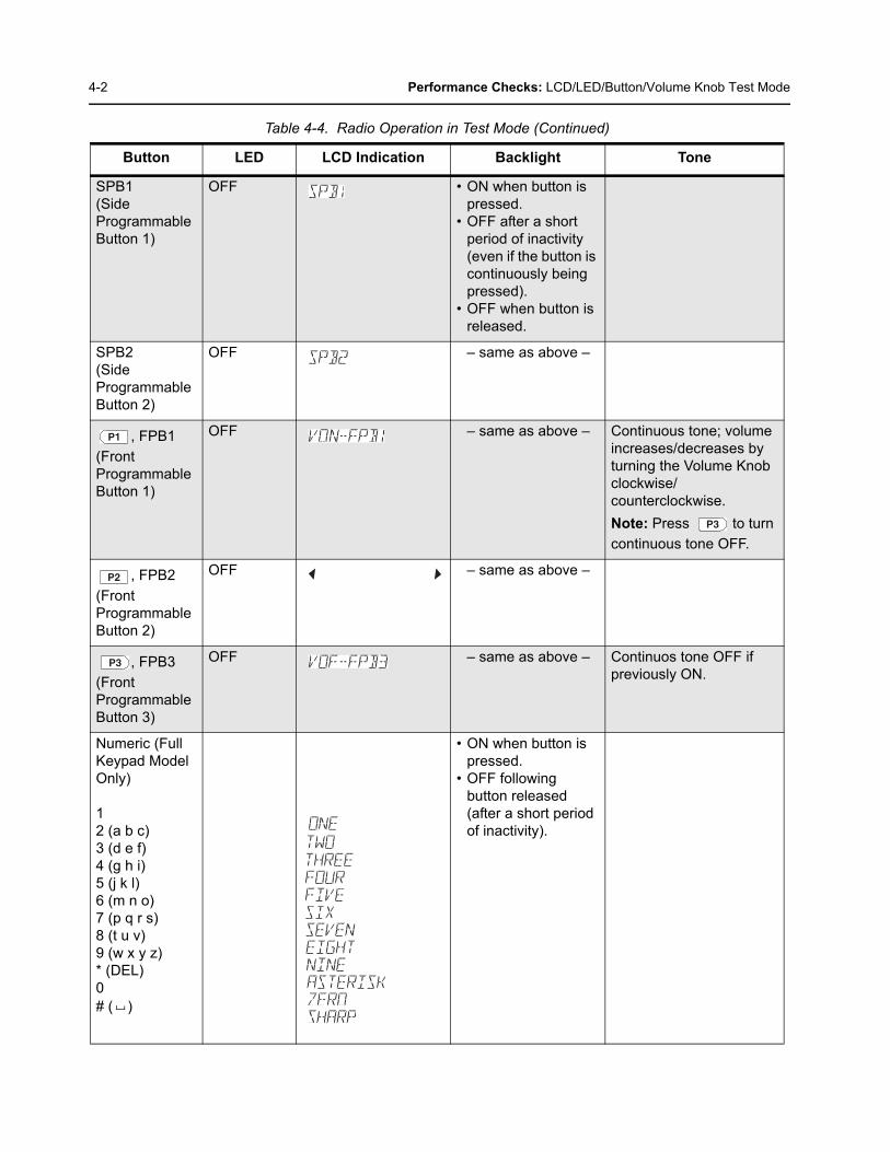
4-2 Performance Checks: LCD/LED/Button/Volume Knob Test Mode
SPB1(Side Programmable Button 1)
OFF • ON when button is pressed.
• OFF after a short period of inactivity (even if the button is continuously being pressed).
• OFF when button is released.
SPB2(Side Programmable Button 2)
OFF – same as above –
, FPB1(Front Programmable Button 1)
OFF – same as above – Continuous tone; volume increases/decreases by turning the Volume Knob clockwise/ counterclockwise.Note: Press to turn continuous tone OFF.
, FPB2(Front Programmable Button 2)
OFF – same as above –
, FPB3(Front Programmable Button 3)
OFF – same as above – Continuos tone OFF if previously ON.
Numeric (Full Keypad Model Only)
12 (a b c)3 (d e f)4 (g h i)5 (j k l)6 (m n o)7 (p q r s)8 (t u v)9 (w x y z)* (DEL)0# ( )
• ON when button is pressed.
• OFF following button released (after a short period of inactivity).
Table 4-4. Radio Operation in Test Mode (Continued)
Button LED LCD Indication Backlight Tone

Performance Checks: LCD/LED/Button/Volume Knob Test Mode 4-3
PTT Button (Push–To–Talk Button)
Solid Amber • ON when button is pressed.
• OFF following button released (After a short period of inactivity)
Table 4-4. Radio Operation in Test Mode (Continued)
Button LED LCD Indication Backlight Tone

4-4 Performance Checks: LCD/LED/Button/Volume Knob Test Mode
Notes
Chapter 5 Radio Programming and Tuning
5.1 IntroductionThis chapter provides an overview of the EP350 Series Customer Programming Software (CPS) and the CP/EP/P Tuner as designed for use in a Windows® 2000/XP/Vista environment. Both cover all the functions of the traditional Radio Service Software (RSS) package.They are both available in the CPS CDROM (PMVN4161_) and Entry Level Radio Tuner CDROM (PMVN4165_).
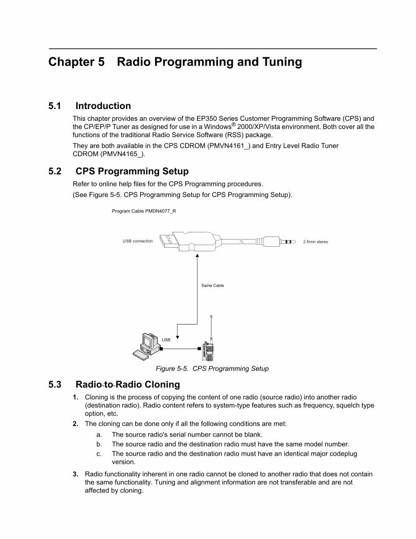
5.2 CPS Programming SetupRefer to online help files for the CPS Programming procedures. (See Figure 5-5. CPS Programming Setup for CPS Programming Setup).
5.3 Radio-to-Radio Cloning1. Cloning is the process of copying the content of one radio (source radio) into another radio
(destination radio). Radio content refers to system-type features such as frequency, squelch type option, etc.
2. The cloning can be done only if all the following conditions are met:a. The source radio's serial number cannot be blank.b. The source radio and the destination radio must have the same model number.c. The source radio and the destination radio must have an identical major codeplug
version.
3. Radio functionality inherent in one radio cannot be cloned to another radio that does not contain the same functionality. Tuning and alignment information are not transferable and are not affected by cloning.
Figure 5-5. CPS Programming Setup
USB
Same Cable
Program Cable PMDN4077_R
2.5mm stereoUSB connection
5-2 Radio Programming and Tuning: Radio Tuning Setup
Procedure:
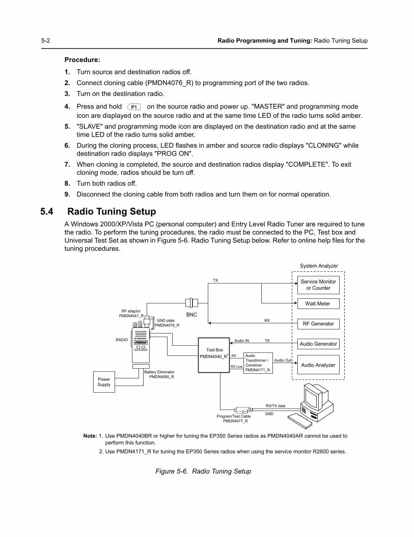
1. Turn source and destination radios off.2. Connect cloning cable (PMDN4076_R) to programming port of the two radios.3. Turn on the destination radio.
4. Press and hold on the source radio and power up. "MASTER" and programming mode icon are displayed on the source radio and at the same time LED of the radio turns solid amber.
5. "SLAVE" and programming mode icon are displayed on the destination radio and at the same time LED of the radio turns solid amber.
6. During the cloning process, LED flashes in amber and source radio displays "CLONING" while destination radio displays "PROG ON".
7. When cloning is completed, the source and destination radios display "COMPLETE". To exit cloning mode, radios should be turn off.
8. Turn both radios off.9. Disconnect the cloning cable from both radios and turn them on for normal operation.
5.4 Radio Tuning SetupA Windows 2000/XP/Vista PC (personal computer) and Entry Level Radio Tuner are required to tune the radio. To perform the tuning procedures, the radio must be connected to the PC, Test box and Universal Test Set as shown in Figure 5-6. Radio Tuning Setup below. Refer to online help files for the tuning procedures.
Figure 5-6. Radio Tuning Setup
RADIO
Power
Supply
BNC
Test Box
PMDN4040_R
Audio IN
RX
RX
RX Low
TX
TX
Audio Out
RX/TX data
GNDProgram/Test Cable
PMDN4077_R
Battery Eliminator
PMDN4080_R
RF adaptor
PMDN4041_R
GND plate
PMDN4079_R
1
Watt Meter
Service Monitor
or Counter
System Analyzer
RF Generator
Audio Generator
Audio Analyzer
Audio
Transformer /
Combiner
PMDN4171_R
Note: 1. Use PMDN4040BR or higher for tuning the EP350 Series radios as PMDN4040AR cannot be used to perform this function.
2. Use PMDN4171_R for tuning the EP350 Series radios when using the service monitor R2600 series.
Radio Programming and Tuning: Transmitter Alignment Options 5-3
5.4.1 Initial Test Equipment Control SettingsThe initial test equipment control settings are listed in Table 5-5.
5.5 Transmitter Alignment Options
Table 5-6. Transmit High/Low Power Level
5.5.1 Transmit High Power Tuning1. Click the Read icon to initiate communication with the radio.2. Under the Alignment menu, select Tx Power, then select High (Figure 5-7. Tx High Power
Window (High Power)).
Table 5-5. Initial Equipment Control Settings
Service Monitor Test Set Power Supply
Monitor Mode: Power Monitor Impedance: 24 Ohm
Voltage: 7.5 Vdc
RF Attenuation: -70 Speaker/load: Load
DC on/standby: Standby
AM, CW, FM: FM PTT: OFF Volt Range: 0 – 10 V
Oscilloscope Source: ModOscilloscope Horizontal: 10 mSec/DivOscilloscope Vertical: 2.5 kHz/DivOscilloscope Trigger: AutoMonitor Image: HiMonitor BW: NarMonitor Squelch: mid CWMonitor Volume: 1/4 CW
Current: 3.0 A
Note: The maximum available power level given in the table below must NOT be exceeded. There are separate alignment procedures for High and Low power.
Note: When checking the RF power output of the radio with a test set, always use a pad of at least 30 dB attached to the radio end of the RF cable. This will avoid an RF mismatch and ensure a stable RF reading that will not change with varying lengths of connecting cable.
RF Band (MHz) Model Number High Power (W)
Low Power (W)
435 – 480M 4W 12.5/25K 99C FKPFPP SCR _H03RDK8AA_ 4.10 – 4.35 1.05 – 1.25
435 – 480M 4W 12.5/25K 99C LKP SCR _H03RDH8AA_ 4.10 – 4.35 1.05 – 1.25
136 – 174M 5W 12.5/25K 99C SCR _H03KEK8AA_ 5.00 – 5.30 1.00 – 1.30
136 – 174M 5W 12.5/25K 99C SCR _H03KEH8AA_ 5.00 – 5.30 1.00 – 1.30
403 – 447M 4W 12.5/25K 99C FKPFPP SCR _H03QDK8AA_ 4.10 – 4.35 1.05 – 1.25
403 – 447M 4W 12.5/25K 99C LKP SCR _H03QDH8AA_ 4.10 – 4.35 1.05 – 1.25

5-4 Radio Programming and Tuning: Transmitter Alignment Options
3. Press PTT Toggle. This will key up the radio at the 1st test frequency (F1).4. Read the Transmit Power from the Service Monitor.5. Adjust the High Power Level as shown in Table 5-6 on page 3 by using either the Left/Right
arrows on the slider or Up/Down arrows on the Working Softpot box. 6. Press PTT Toggle to dekey the radio.7. Goto the next frequency point by clicking on the next Working Softpot value and press PTT
Toggle.8. Repeat steps 4 – 6 for the remaining test frequencies (F2–F5).9. Press Program to commit the softpot values into the codeplug.10. Exit the Transmit High Power function.11. If the radio uses only high power channels, proceed to adjust modulation. If low power channels
are used, perform Transmit Low Power Tuning as defined.
5.5.2 Transmit Low Power Tuning1. Click the Read icon to initiate communication with the radio.2. Under the Alignment menu, select Tx Power, then select Low (Figure 5-8. Tx Low Power
Window (Low Power)).3. Press PTT Toggle. This will key up the radio at the 1st test frequency (F1).4. Read the Transmit Power from the Service Monitor.5. Adjust the Low Power Level as shown in Table 5-6 on page 3 by using either the Left/Right
arrows on the slider or Up/Down arrows on the Working Softpot box. 6. Press PTT Toggle to dekey the radio.7. Goto the next frequency point by clicking on the next Working Softpot value and press PTT
Toggle.8. Repeat steps 4–6 for the remaining test frequencies (F2–F5).9. Press Program to commit the softpot values into the codeplug.10. Exit the Transmit Low Power function.11. Proceed to Adjust Modulation.
Figure 5-7. Tx High Power Window (High Power)
F1F2
F3F4F5

Radio Programming and Tuning: Transmitter Alignment Options 5-5
5.5.3 Transmit Modulation TuningThere are 2 variations of Transmit Modulation Tuning, namely 12.5 kHz and 25 kHz.
Table 5-7. Transmit Modulation Tuning
5.5.3.1 Service Monitor Setting1. Initial setup using the 8920A RF Communications Test Set
a. Connect “RF IN/OUT” port on 8920A to RF adaptor on radio’s antenna port using a N-Type to BNC cable. Connect “AUDIO OUT” on 8920A to “Tx MOD” on test box using a BNC to BNC cable. Connect the rest according to Figure 5-6. Radio Tuning Setup.
b. On 8920A, select “Tx” under “SCREEN CONTROL”.
c. Using the “CURSOR CONTROL”, key in the following items:
i. Tune Mode: Auto
ii. Tune Freq: Depends on Tune Mode
- Once “Auto” is selected, the centre frequency is set to the strongest RF signal- Once “Manual” is selected, desired frequency has to be entered manually
iii. Tx Pwr Zero: Zero
iv. Input Port: RF In
v. Ext Tx Key: Off
Figure 5-8. Tx Low Power Window (Low Power)
Channel Spacing (kHz) Tuning Range (kHz)
12.5 2.25 ± 0.05
25 4.5 ± 0.1
F1F2
F3F4F5
5-6 Radio Programming and Tuning: Transmitter Alignment Options
vi. AF An1 In: FM Demod
vii. Filter 1: 50 Hz HPF
viii. Filter 2: 15 kHz LPF
ix. De-Emphasis: 750us
x. Detector: Pk+-Max
xi. AFGen1 Freq: 1.0000 kHz
xii. AFGen1 Lvl: 100mV
2. Initial setup using the R2600 series RF Communications Test Seta. Connect “RF IN/OUT” port on R2600 series to RF adaptor on radio’s antenna port using a N-
Type to BNC cable. Connect “MOT OUT” on R2600 series to “Tx MOD” on test box using a BNC to BNC cable. Connect the rest according to Figure 5-6. Radio Tuning Setup.
b. On R2600, select “DISP” under “CURSOR ZONE”:
i. Meter: RF DISPLAY
ii. Mode: STANDARD
iii. Dev: (Reading for Transmit Modulation)
c. On R2600, select “RF” under “CURSOR ZONE”:
i. RF Control: MONITOR
ii. Preset: --
iii. B/W: NB
iv. Freq: Frequency Point (F1–F5) on Tuner
v. Output Lvl: 20dBm
vi. Gen RF Out: RF I/O
vii. Modulation Type: FM
d. On R2600, select “AUD” under “CURSOR ZONE”:
i. Fixed 1kHz: 0.100V. Enable (~)
ii. Synth: Disable (x)
iii. DTMF: Disable (x)
iv. External: Disable (x)
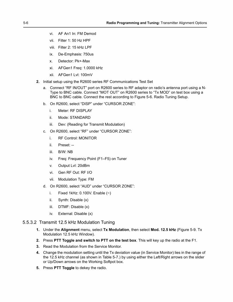
5.5.3.2 Transmit 12.5 kHz Modulation Tuning1. Under the Alignment menu, select Tx Modulation, then select Mod. 12.5 kHz (Figure 5-9. Tx
Modulation 12.5 kHz Window).2. Press PTT Toggle and switch to PTT on the test box. This will key up the radio at the F1.3. Read the Modulation from the Service Monitor.4. Change the modulation setting until the Tx deviation value (in Service Monitor) lies in the range of
the 12.5 kHz channel (as shown in Table 5-7.) by using either the Left/Right arrows on the slider or Up/Down arrows on the Working Softpot box.
5. Press PTT Toggle to dekey the radio.
Radio Programming and Tuning: Transmitter Alignment Options 5-7
6. Go to the next frequency point by clicking on the next Working Softpot value and press PTT Toggle.
7. Repeat steps 3–5 for the remaining test frequencies (F2–F5).8. Press Program to commit the softpot values into the codeplug.9. Exit the Transmit 12.5 kHz Modulation function.10. If 25 kHz channels are used, perform Transmit 25 kHz Modulation Tuning.
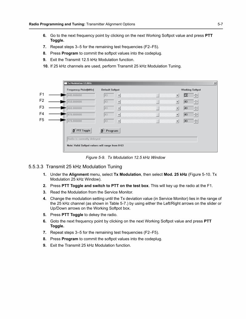
5.5.3.3 Transmit 25 kHz Modulation Tuning1. Under the Alignment menu, select Tx Modulation, then select Mod. 25 kHz (Figure 5-10. Tx
Modulation 25 kHz Window).2. Press PTT Toggle and switch to PTT on the test box. This will key up the radio at the F1.3. Read the Modulation from the Service Monitor.4. Change the modulation setting until the Tx deviation value (in Service Monitor) lies in the range of
the 25 kHz channel (as shown in Table 5-7.) by using either the Left/Right arrows on the slider or Up/Down arrows on the Working Softpot box.
5. Press PTT Toggle to dekey the radio.6. Goto the next frequency point by clicking on the next Working Softpot value and press PTT
Toggle.7. Repeat steps 3–5 for the remaining test frequencies (F2–F5).8. Press Program to commit the softpot values into the codeplug.9. Exit the Transmit 25 kHz Modulation function.
Figure 5-9. Tx Modulation 12.5 kHz Window
F1F2
F3F4F5

5-8 Radio Programming and Tuning: Receiver Tuning
5.6 Receiver TuningThere are 4 variations of Receive Squelch Tuning: 12.5 kHz-Band Normal Squelch, 12.5 kHz-Band Tight Squelch, 25 kHz-Band Normal Squelch and 25 kHz-Band Tight Squelch.
5.6.1 Service Monitor Setting1. Initial setup using the 8920A RF Communications Test Set
a. Connect “RF IN/OUT” port on 8920A to RF adaptor on radio’s antenna port using a N-Type to BNC cable. Connect “AUDIO IN” HI and LO on 8920A to “Rx Audio” on test box using two BNC to BNC cables. Connect the rest according to Figure 5-6. Radio Tuning Setup.
b. On 8920A, press “Rx” under “SCREEN CONTROL”.
c. Using the “CURSOR CONTROL”, key in the items below:
i. RF Gen Freq: Frequency Point (F1 – F5) on Tuner
ii. Amplitude: -128dBm
iii. Atten Hold: Off
iv. Output Port: RF Out
v. AFGen1 Freq: 1.0000 kHz
vi. AFGen1 To: 1.5 kHz for 12.5 kHz channel spacing, 3.0 kHz for 25 kHz channel spacing
vii. AFGen2 Freq: 0.0000 kHz
viii. AFGen2 To: Off
ix. Filter 1: 50 Hz HPF
Figure 5-10. Tx Modulation 25 kHz Window
Table 5-8. Receiver Squelch Tuning
Squelch Type Tuning Range (dB)
Normal 6 – 8
Tight 15 – 17
F1F2
F3F4F5

Radio Programming and Tuning: Receiver Tuning 5-9
x. Filter 2: 15 kHz LPF
xi. Ext Load R: 24 Ω
2. Initial setup using the R2600 series RF Communications Test Seta. Connect “RF IN/OUT” port on R2600 series to RF adaptor on radio’s antenna port using a N-
Type to BNC cable. Connect “VERT/SINAD DIST/DVM COUNTER IN” on R2600 series to the single input on audio transformer using one BNC to BNC cable. Connect the rest according to Figure 5-6. Radio Tuning Setup.
b. On R2600, select “DISP” under “CURSOR ZONE”
i. Meter: SINAD
ii. Mode: STANDARD
c. On R2600, select “RF” under “CURSOR ZONE”:
i. RF Control: GENERATE
ii. Preset: --
iii. B/W: NB
iv. Freq: Frequency Point (F1–F5) on Tuner
v. Output Lvl: -128dBm (refer to step 2 in Section 5.6.2) and increase slowly (-127dBm, -126dBm…) (refer to step 3 in Section 5.6.2)
vi. Gen RF Out: RF I/O
vii. Modulation Type: FM
d. On R2600, select “AUD” under “CURSOR ZONE”:
i. Fixed 1kHz: 1.50 kHz for 12.5kHz channel spacing and 3.0 kHz for 25kHz channel spacing. Enable (~)
ii. Synth: Disable (x)
iii. DTMF: Disable (x)
iv. External: Disable (x)
5.6.2 Receive 12.5 kHz-Band Normal Squelch Tuning1. Under the Alignment menu, select Rx Squelch, then select Squelch 12.5 kHz-band Normal.
(Figure 5-11. Rx 12.5 kHz-band Normal Squelch Tuning Window).2. Apply a RF signal (with 1 kHz tone at 1.5 kHz deviation) for current frequency point with minimum
amplitude, -128 dBm (F1 being the first). 3. Set softpot to minimum (0) and adjust the amplitude of RF signal to the range of normal squelch
tuning (as shown in Table 5-8.) on the test equipment.4. Adjust the softpot value by using either the Left/Right arrows on the slider or Up/Down arrows on
the Working Softpot box until the radio is totally muted.5. Repeat steps 2–4 for F2–F5.6. Press Program to commit the softpot values into the codeplug.
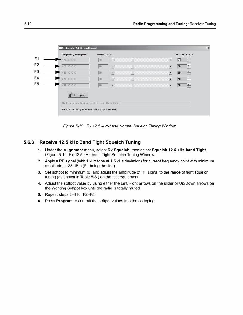
5-10 Radio Programming and Tuning: Receiver Tuning
5.6.3 Receive 12.5 kHz-Band Tight Squelch Tuning1. Under the Alignment menu, select Rx Squelch, then select Squelch 12.5 kHz-band Tight.
(Figure 5-12. Rx 12.5 kHz-band Tight Squelch Tuning Window).2. Apply a RF signal (with 1 kHz tone at 1.5 kHz deviation) for current frequency point with minimum
amplitude, -128 dBm (F1 being the first). 3. Set softpot to minimum (0) and adjust the amplitude of RF signal to the range of tight squelch
tuning (as shown in Table 5-8.) on the test equipment.4. Adjust the softpot value by using either the Left/Right arrows on the slider or Up/Down arrows on
the Working Softpot box until the radio is totally muted.5. Repeat steps 2–4 for F2–F5.6. Press Program to commit the softpot values into the codeplug.
Figure 5-11. Rx 12.5 kHz-band Normal Squelch Tuning Window
F1F2
F3F4F5
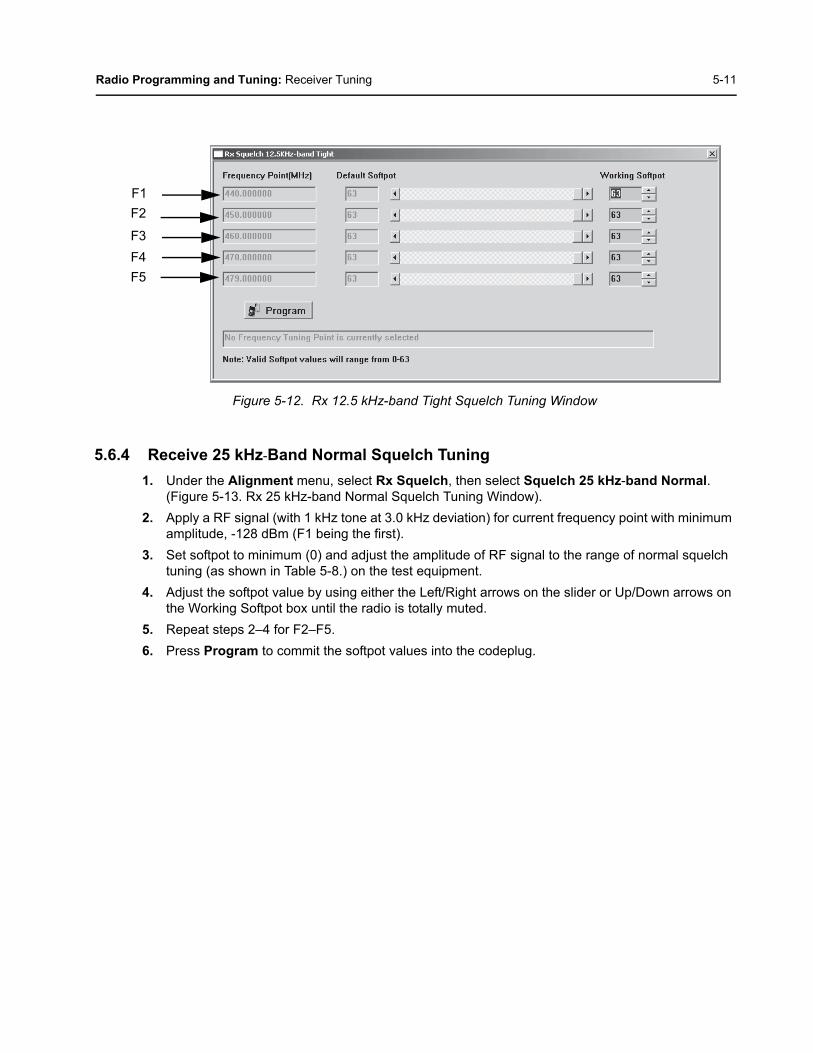
Radio Programming and Tuning: Receiver Tuning 5-11
5.6.4 Receive 25 kHz-Band Normal Squelch Tuning1. Under the Alignment menu, select Rx Squelch, then select Squelch 25 kHz-band Normal.
(Figure 5-13. Rx 25 kHz-band Normal Squelch Tuning Window).2. Apply a RF signal (with 1 kHz tone at 3.0 kHz deviation) for current frequency point with minimum
amplitude, -128 dBm (F1 being the first). 3. Set softpot to minimum (0) and adjust the amplitude of RF signal to the range of normal squelch
tuning (as shown in Table 5-8.) on the test equipment.4. Adjust the softpot value by using either the Left/Right arrows on the slider or Up/Down arrows on
the Working Softpot box until the radio is totally muted.5. Repeat steps 2–4 for F2–F5.6. Press Program to commit the softpot values into the codeplug.
Figure 5-12. Rx 12.5 kHz-band Tight Squelch Tuning Window
F1F2
F3F4F5
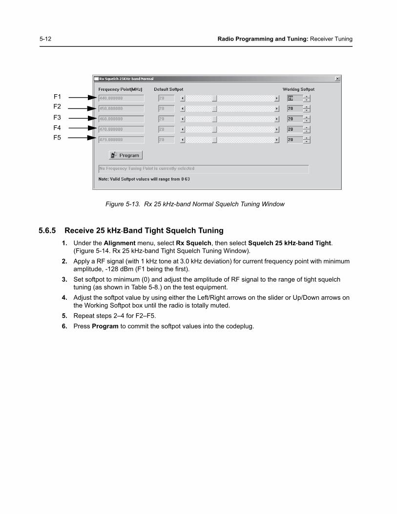
5-12 Radio Programming and Tuning: Receiver Tuning
5.6.5 Receive 25 kHz-Band Tight Squelch Tuning1. Under the Alignment menu, select Rx Squelch, then select Squelch 25 kHz-band Tight.
(Figure 5-14. Rx 25 kHz-band Tight Squelch Tuning Window).2. Apply a RF signal (with 1 kHz tone at 3.0 kHz deviation) for current frequency point with minimum
amplitude, -128 dBm (F1 being the first). 3. Set softpot to minimum (0) and adjust the amplitude of RF signal to the range of tight squelch
tuning (as shown in Table 5-8.) on the test equipment.4. Adjust the softpot value by using either the Left/Right arrows on the slider or Up/Down arrows on
the Working Softpot box until the radio is totally muted.5. Repeat steps 2–4 for F2–F5.6. Press Program to commit the softpot values into the codeplug.
Figure 5-13. Rx 25 kHz-band Normal Squelch Tuning Window
F1F2
F3F4F5
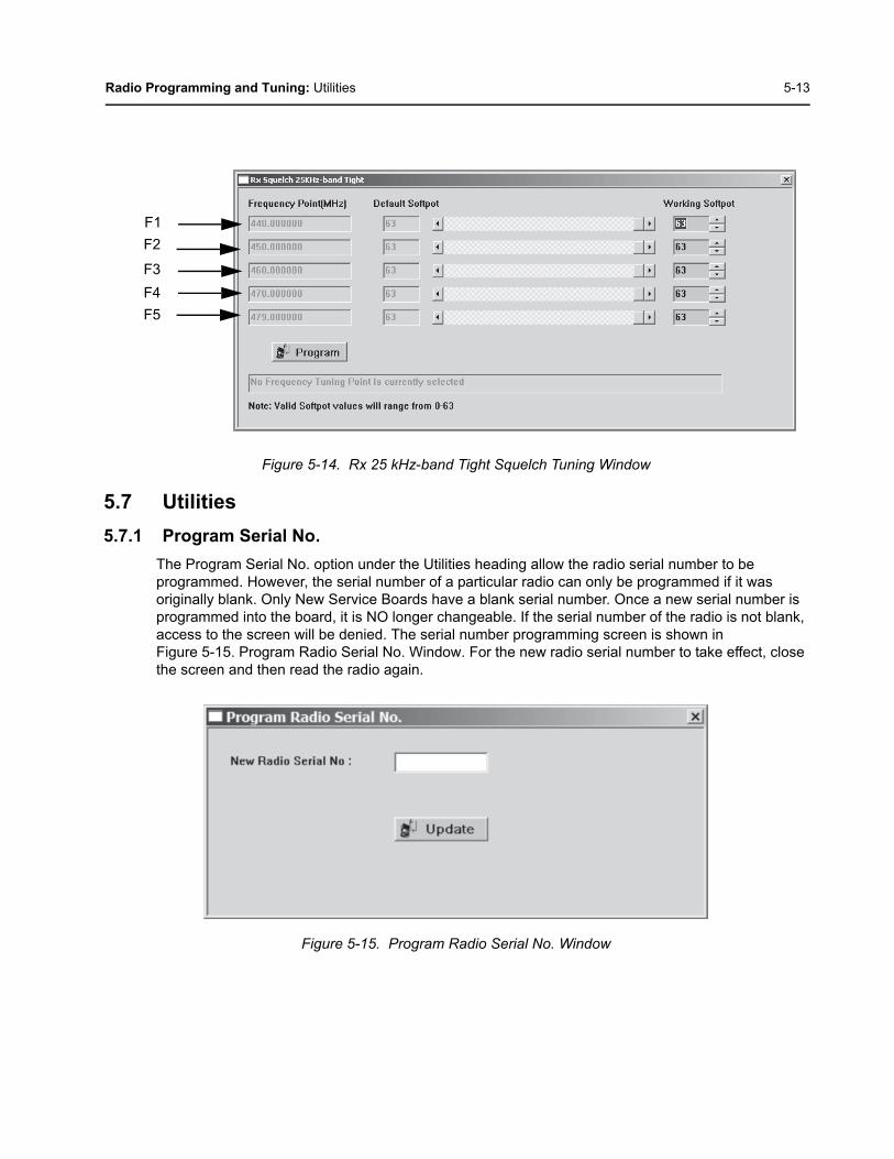
Radio Programming and Tuning: Utilities 5-13
5.7 Utilities5.7.1 Program Serial No.
The Program Serial No. option under the Utilities heading allow the radio serial number to be programmed. However, the serial number of a particular radio can only be programmed if it was originally blank. Only New Service Boards have a blank serial number. Once a new serial number is programmed into the board, it is NO longer changeable. If the serial number of the radio is not blank, access to the screen will be denied. The serial number programming screen is shown in Figure 5-15. Program Radio Serial No. Window. For the new radio serial number to take effect, close the screen and then read the radio again.
Figure 5-14. Rx 25 kHz-band Tight Squelch Tuning Window
Figure 5-15. Program Radio Serial No. Window
F1F2
F3F4F5
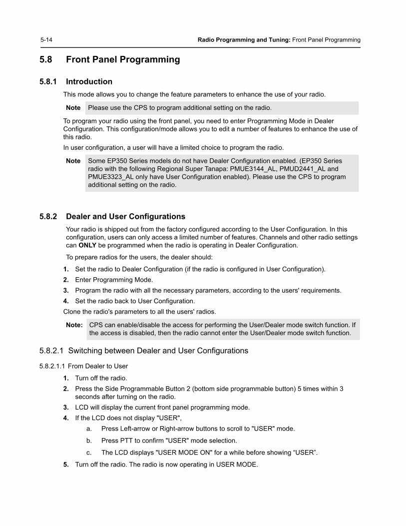
5-14 Radio Programming and Tuning: Front Panel Programming
5.8 Front Panel Programming
5.8.1 IntroductionThis mode allows you to change the feature parameters to enhance the use of your radio.
To program your radio using the front panel, you need to enter Programming Mode in Dealer Configuration. This configuration/mode allows you to edit a number of features to enhance the use of this radio.In user configuration, a user will have a limited choice to program the radio.
5.8.2 Dealer and User ConfigurationsYour radio is shipped out from the factory configured according to the User Configuration. In this configuration, users can only access a limited number of features. Channels and other radio settings can ONLY be programmed when the radio is operating in Dealer Configuration.
To prepare radios for the users, the dealer should:
1. Set the radio to Dealer Configuration (if the radio is configured in User Configuration).2. Enter Programming Mode.3. Program the radio with all the necessary parameters, according to the users' requirements.4. Set the radio back to User Configuration.Clone the radio's parameters to all the users' radios.
5.8.2.1 Switching between Dealer and User Configurations
5.8.2.1.1 From Dealer to User
1. Turn off the radio.2. Press the Side Programmable Button 2 (bottom side programmable button) 5 times within 3
seconds after turning on the radio.3. LCD will display the current front panel programming mode.4. If the LCD does not display "USER",
a. Press Left-arrow or Right-arrow buttons to scroll to "USER" mode.
b. Press PTT to confirm "USER" mode selection.
c. The LCD displays "USER MODE ON" for a while before showing “USER”.
5. Turn off the radio. The radio is now operating in USER MODE.
Note Please use the CPS to program additional setting on the radio.
Note Some EP350 Series models do not have Dealer Configuration enabled. (EP350 Series radio with the following Regional Super Tanapa: PMUE3144_AL, PMUD2441_AL and PMUE3323_AL only have User Configuration enabled). Please use the CPS to program additional setting on the radio.
Note: CPS can enable/disable the access for performing the User/Dealer mode switch function. If the access is disabled, then the radio cannot enter the User/Dealer mode switch function.
Radio Programming and Tuning: Front Panel Programming 5-15
5.8.2.1.2 From User to Dealer
1. Turn off the radio.2. Press the Side Programmable Button 2 (bottom side programmable button) 5 times within 3
seconds after turning on the radio.3. LCD will display the current front panel programming mode.4. If the LCD does not display "DEALER",
a. Press Left-arrow or Right-arrow buttons to scroll to "DEALER" mode.
b. Press PTT to confirm "DEALER" mode selection.
c. The LCD displays "DEALER MODE ON" for a while before showing “DEALER”.
5. Turn off the radio. The radio is now operating in DEALER MODE.
5.8.3 Entering Programming ModeMake sure the radio is turn off. Press Side Programmable Button 1 (top side programmable button), and turn ON the radio. A tone is heard, indicating that the radio is in Programming Mode. The indicator illuminates and the "BCKLIGHT" is displayed on the radio LCD.
5.8.4 Exiting Programming ModeTurn off the radio to exit Programming Mode.
5.8.5 Accessing Front Panel Programming Mode ParametersPress or to scroll through the parameters for each menu or sub-menu item, or Press PTT to select the menu or sub-menu item, or
Press Side Programmable Button 1 to either return to previous menu level or to exit the selection parameter without change.
Important: If the radio is to be given to the customer, REMEMBER to switch it back to operate in User Configuration.
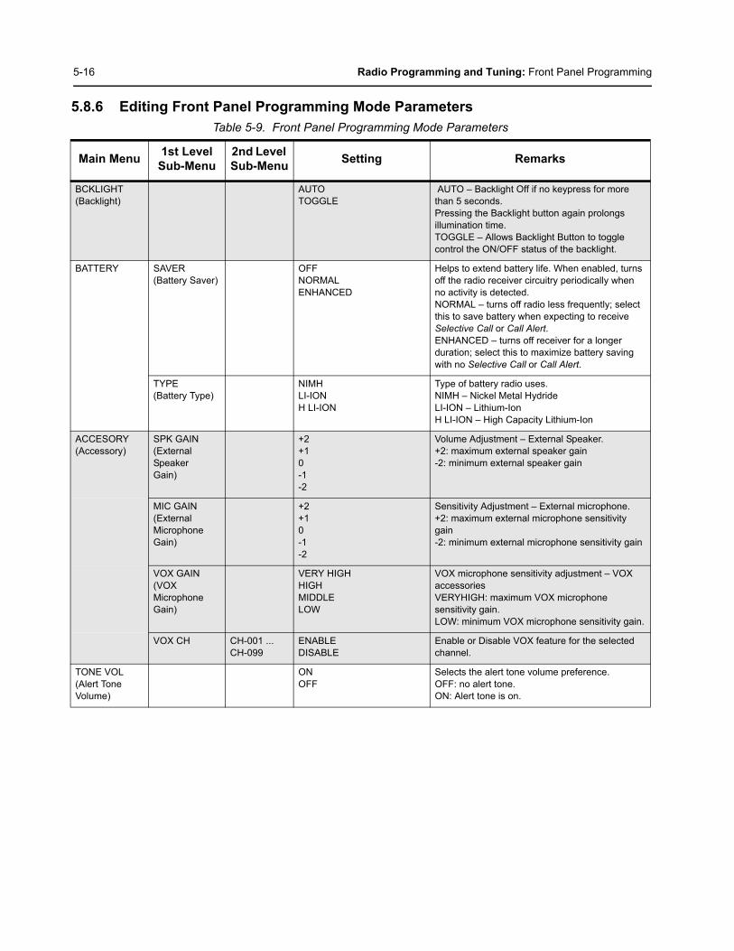
5-16 Radio Programming and Tuning: Front Panel Programming
5.8.6 Editing Front Panel Programming Mode ParametersTable 5-9. Front Panel Programming Mode Parameters
Main Menu 1st Level Sub-Menu
2nd Level Sub-Menu Setting Remarks
BCKLIGHT(Backlight)
AUTOTOGGLE
AUTO – Backlight Off if no keypress for more than 5 seconds.Pressing the Backlight button again prolongs illumination time.TOGGLE – Allows Backlight Button to toggle control the ON/OFF status of the backlight.
BATTERY SAVER(Battery Saver)
OFFNORMALENHANCED
Helps to extend battery life. When enabled, turns off the radio receiver circuitry periodically when no activity is detected.NORMAL – turns off radio less frequently; select this to save battery when expecting to receive Selective Call or Call Alert.ENHANCED – turns off receiver for a longer duration; select this to maximize battery saving with no Selective Call or Call Alert.
TYPE(Battery Type)
NIMH LI-IONH LI-ION
Type of battery radio uses.NIMH – Nickel Metal HydrideLI-ION – Lithium-IonH LI-ION – High Capacity Lithium-Ion
ACCESORY(Accessory)
SPK GAIN(External SpeakerGain)
+2+10-1-2
Volume Adjustment – External Speaker.+2: maximum external speaker gain-2: minimum external speaker gain
MIC GAIN(ExternalMicrophone Gain)
+2+10-1-2
Sensitivity Adjustment – External microphone.+2: maximum external microphone sensitivity gain-2: minimum external microphone sensitivity gain
VOX GAIN(VOX MicrophoneGain)
VERY HIGHHIGHMIDDLELOW
VOX microphone sensitivity adjustment – VOXaccessoriesVERYHIGH: maximum VOX microphone sensitivity gain. LOW: minimum VOX microphone sensitivity gain.
VOX CH CH-001 ...CH-099
ENABLEDISABLE
Enable or Disable VOX feature for the selected channel.
TONE VOL(Alert Tone Volume)
ONOFF
Selects the alert tone volume preference.OFF: no alert tone.ON: Alert tone is on.
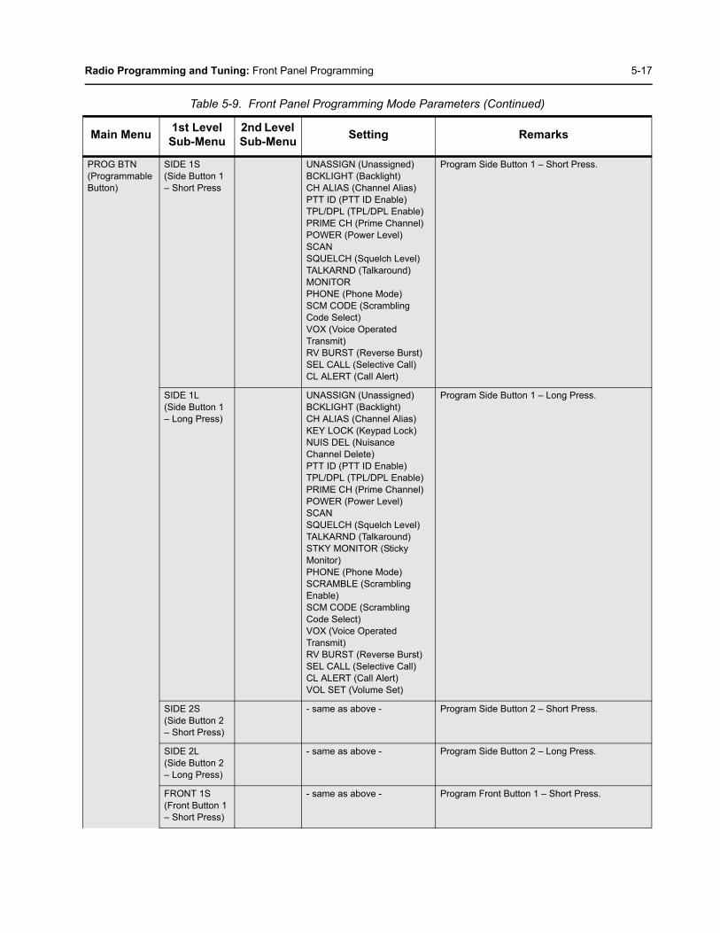
Radio Programming and Tuning: Front Panel Programming 5-17
PROG BTN(ProgrammableButton)
SIDE 1S(Side Button 1 – Short Press
UNASSIGN (Unassigned)BCKLIGHT (Backlight)CH ALIAS (Channel Alias)PTT ID (PTT ID Enable)TPL/DPL (TPL/DPL Enable)PRIME CH (Prime Channel)POWER (Power Level)SCANSQUELCH (Squelch Level)TALKARND (Talkaround) MONITORPHONE (Phone Mode)SCM CODE (Scrambling Code Select)VOX (Voice Operated Transmit)RV BURST (Reverse Burst)SEL CALL (Selective Call)CL ALERT (Call Alert)
Program Side Button 1 – Short Press.
SIDE 1L(Side Button 1 – Long Press)
UNASSIGN (Unassigned)BCKLIGHT (Backlight)CH ALIAS (Channel Alias)KEY LOCK (Keypad Lock)NUIS DEL (Nuisance Channel Delete)PTT ID (PTT ID Enable)TPL/DPL (TPL/DPL Enable)PRIME CH (Prime Channel)POWER (Power Level)SCANSQUELCH (Squelch Level)TALKARND (Talkaround)STKY MONITOR (Sticky Monitor)PHONE (Phone Mode)SCRAMBLE (Scrambling Enable)SCM CODE (Scrambling Code Select)VOX (Voice Operated Transmit)RV BURST (Reverse Burst)SEL CALL (Selective Call)CL ALERT (Call Alert)VOL SET (Volume Set)
Program Side Button 1 – Long Press.
SIDE 2S(Side Button 2 – Short Press)
- same as above - Program Side Button 2 – Short Press.
SIDE 2L(Side Button 2 – Long Press)
- same as above - Program Side Button 2 – Long Press.
FRONT 1S(Front Button 1 – Short Press)
- same as above - Program Front Button 1 – Short Press.
Table 5-9. Front Panel Programming Mode Parameters (Continued)
Main Menu 1st Level Sub-Menu
2nd Level Sub-Menu Setting Remarks
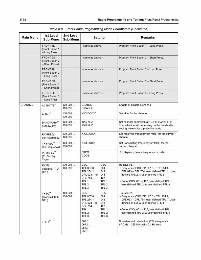
5-18 Radio Programming and Tuning: Front Panel Programming
FRONT 1L(Front Button 1 – Long Press)
- same as above - Program Front Button 1 – Long Press.
FRONT 2S(Front Button 2 – Short Press)
- same as above - Program Front Button 2 – Short Press.
FRONT 2L(Front Button 2 – Long Press)
- same as above - Program Front Button 2 – Long Press.
FRONT 3S(Front Button 3 – Short Press)
- same as above - Program Front Button 3 – Short Press.
FRONT 3L(Front Button 3 – Long Press)
- same as above - Program Front Button 3 – Long Press.
CHANNEL ACTIVATE** CH-001 ...CH-099
ENABLEDISABLE
Enable or disable a channel.
ALIAS** CH-001 ...CH-099
YYYYYYYY Set alias for the channel.
BANDWDTH**
(Bandwidth)CH-001 ...CH-099
12.5 KHZ25.0 KHZ
Set channel bandwidth at 12.5 kHz or 25 kHz. The selection will depending on the bandwidth setting allowed for a particular mode
RX FREQ**
(Rx Frequency)CH-001 ...CH-099
XXX. XXXX Set receiving frequency (in MHz) for the current channel.
TX FREQ**
(Tx Frequency)CH-001 ...CH-099
XXX. XXXX Set transmitting frequency (in MHz) for the current channel.
PL DSPLY**
(PL Display Type)
FREQCODE
PL display type – in frequency or code.
RX PL**
(Receive TPL/DPL)
CH-001 ...CH-099
CSQ CSQTPL 067.0 ... 001 ...TPL 254.1 042DPL 023 or 043 DPL 754 127TPL 1 TPL 1TPL 2 TPL 2TPL 3 TPL 3
Receive PL•Frequency: CSQ, TPL 67.0 – TPL 254.1, DPL 023 – DPL 754, user defined TPL 1, user defined TPL 2, & user defined TPL 3
•Code: CSQ, 001 – 127, user defined TPL 1,user defined TPL 2, & user defined TPL 3
TX PL**
(Transmit TPL/DPL)
CH-001 ...CH-099
CSQ CSQTPL 067.0 001 ...TPL 254.1 042DPL 023 or 043 DPL 754 127TPL 1 TPL 1TPL 2 TPL 2TPL 3 TPL 3
Transmit PL•Frequency: CSQ, TPL 67.0 – TPL 254.1, DPL 023 – DPL 754, user defined TPL 1, user defined TPL 2, & user defined TPL 3
•Code: CSQ, 001 – 127, user defined TPL 1,user defined TPL 2, & user defined TPL 3
TPL 1** 067.0067.1 ...254.9255.0
Non-standard private line (TPL) frequency.67.0 Hz – 255.0 Hz with 0.1 Hz step.
Table 5-9. Front Panel Programming Mode Parameters (Continued)
Main Menu 1st Level Sub-Menu
2nd Level Sub-Menu Setting Remarks
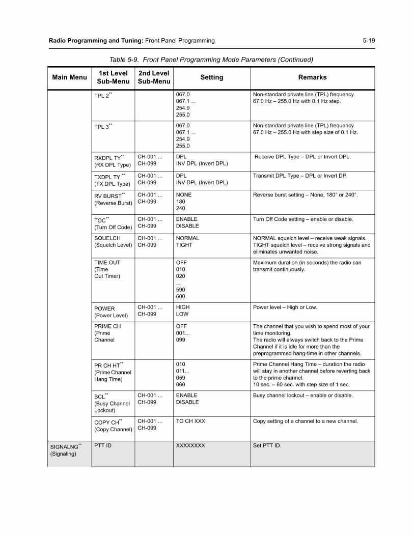
Radio Programming and Tuning: Front Panel Programming 5-19
TPL 2** 067.0067.1 ...254.9255.0
Non-standard private line (TPL) frequency.67.0 Hz – 255.0 Hz with 0.1 Hz step.
TPL 3** 067.0067.1 ...254.9255.0
Non-standard private line (TPL) frequency.67.0 Hz – 255.0 Hz with step size of 0.1 Hz.
RXDPL TY**
(RX DPL Type)CH-001 ...CH-099
DPLINV DPL (Invert DPL)
Receive DPL Type – DPL or Invert DPL.
TXDPL TY **(TX DPL Type)
CH-001 ...CH-099
DPLINV DPL (Invert DPL)
Transmit DPL Type – DPL or Invert DP.
RV BURST**
(Reverse Burst)CH-001 ...CH-099
NONE180240
Reverse burst setting – None, 180° or 240°.
TOC**
(Turn Off Code)CH-001 ...CH-099
ENABLEDISABLE
Turn Off Code setting – enable or disable.
SQUELCH(Squelch Level)
CH-001 ...CH-099
NORMALTIGHT
NORMAL squelch level – receive weak signals. TIGHT squelch level – receive strong signals and eliminates unwanted noise.
TIME OUT (TimeOut Timer)
OFF010020...590600
Maximum duration (in seconds) the radio can transmit continuously.
POWER(Power Level)
CH-001 ...CH-099
HIGHLOW
Power level – High or Low.
PRIME CH (PrimeChannel
OFF001...099
The channel that you wish to spend most of your time monitoring. The radio will always switch back to the Prime Channel if it is idle for more than the preprogrammed hang-time in other channels.
PR CH HT**
(Prime Channel Hang Time)
010011...059060
Prime Channel Hang Time – duration the radio will stay in another channel before reverting back to the prime channel. 10 sec. – 60 sec. with step size of 1 sec.
BCL**
(Busy Channel Lockout)
CH-001 ...CH-099
ENABLEDISABLE
Busy channel lockout – enable or disable.
COPY CH**
(Copy Channel)CH-001 ...CH-099
TO CH XXX Copy setting of a channel to a new channel.
SIGNALNG**
(Signaling)PTT ID XXXXXXXX Set PTT ID.
Table 5-9. Front Panel Programming Mode Parameters (Continued)
Main Menu 1st Level Sub-Menu
2nd Level Sub-Menu Setting Remarks
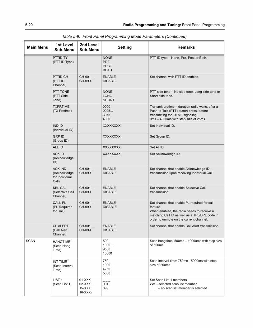
5-20 Radio Programming and Tuning: Front Panel Programming
PTTID TY(PTT ID Type)
NONEPREPOSTBOTH
PTT ID type – None, Pre, Post or Both.
PTTID CH(PTT ID Channel)
CH-001 ...CH-099
ENABLEDISABLE
Set channel with PTT ID enabled.
PTT TONE(PTT Side Tone)
NONELONGSHORT
PTT side tone – No side tone, Long side tone or Short side tone.
TXPRTIME(TX Pretime)
00000025...39754000
Transmit pretime – duration radio waits, after a Push-to-Talk (PTT) button press, before transmitting the DTMF signaling. 0ms – 4000ms with step size of 25ms.
IND ID(Individual ID)
XXXXXXXX Set Individual ID.
GRP ID(Group ID)
XXXXXXXX Set Group ID.
ALL ID XXXXXXXX Set All ID.
ACK ID(Acknowledge ID)
XXXXXXXX Set Acknowledge ID.
ACK IND(Acknowledge for Individual Call)
CH-001 ...CH-099
ENABLEDISABLE
Set channel that enable Acknowledge ID transmission upon receiving Individual Call.
SEL CAL(Selective Call Channel)
CH-001 ...CH-099
ENABLEDISABLE
Set channel that enable Selective Call transmission.
CALL PL(PL Required for Call)
CH-001 ...CH-099
ENABLEDISABLE
Set channel that enable PL required for call feature. When enabled, the radio needs to receive a matching Call ID as well as a TPL/DPL code in order to unmute on the current channel.
CL ALERT(Call Alert Channel)
CH-001 ...CH-099
ENABLEDISABLE
Set channel that enable Call Alert transmission.
SCAN HANGTIME**
(Scan Hang Time)
500 1000 ... 950010000
Scan hang time: 500ms – 10000ms with step size of 500ms.
INT TIME**
(Scan Interval Time)
7501000 ...47505000
Scan interval time: 750ms - 5000ms with step size of 250ms.
LIST 1(Scan List 1)
01-XXX02-XXX ...15-XXX16-XXX\
_ _ _001 ... 099
Set Scan List 1 members.xxx – selected scan list member_ _ _ – no scan list member is selected
Table 5-9. Front Panel Programming Mode Parameters (Continued)
Main Menu 1st Level Sub-Menu
2nd Level Sub-Menu Setting Remarks

Radio Programming and Tuning: Front Panel Programming 5-21
LIST 2(Scan List 2)
01-XXX02-XXX ...15-XXX16-XXX\
_ _ _001 ... 099
Set Scan List 2 members.xxx – selected scan list member_ _ _ – no scan list member is selected
LIST 3(Scan List 3)
01-XXX02-XXX ...15-XXX16-XXX\
_ _ _001 ... 099
Set Scan List 3 members.xxx – selected scan list member_ _ _ – no scan list member is selected
LIST SEL(Scan List Select)
CH-001 ...CH-099
LIST1 (Scan List 1)LIST2 (Scan List 2)LIST3 (Scan List 3)
Set scan list for a selected channel.
SCAN TYP(Scan TypeSelect)
CH-001 ...CH-099
NORMALPRIORITY
Scan type for selected channel – Normal Scan, Priority Scan
PRIORITY(Priority ChannelSelect)
LIST1(Scan List 1)
_ _ _001 ... 099
Set Priority Channel for Scan List 1.xxx – selected priority channel_ _ _ – no priority channel is selected
LIST2(Scan List 2)
_ _ _001 ... 099
Set Priority Channel for Scan List 2.xxx – selected priority channel_ _ _ – no priority channel is selected
LIST3(Scan List 3)
_ _ _001 ... 099
Set Priority Channel for Scan List 3.xxx – selected priority channel_ _ _ – no priority channel is selected
SCRMBLIN(Voice InversionScrambling)
CHANNEL(ScramblingChannel Select)
CH-001 ...CH-099
ENABLEDISABLE
Scrambling – Enable or disable
CODE(Scrambling CodeSelect)
3.293.39
Scrambling code – 3.29 or 3.39.
Table 5-9. Front Panel Programming Mode Parameters (Continued)
Main Menu 1st Level Sub-Menu
2nd Level Sub-Menu Setting Remarks
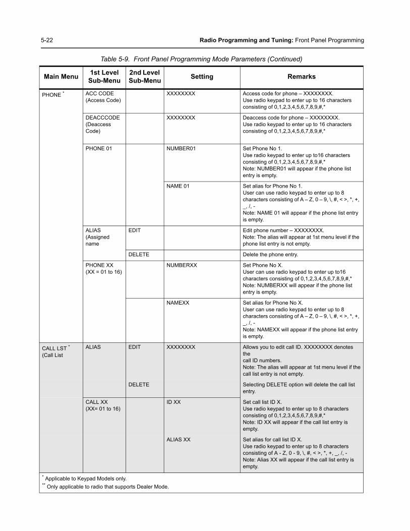
5-22 Radio Programming and Tuning: Front Panel Programming
PHONE * ACC CODE(Access Code)
XXXXXXXX Access code for phone – XXXXXXXX. Use radio keypad to enter up to 16 characters consisting of 0,1,2,3,4,5,6,7,8,9,#,*
DEACCCODE(Deaccess Code)
XXXXXXXX Deaccess code for phone – XXXXXXXX.Use radio keypad to enter up to 16 characters consisting of 0,1,2,3,4,5,6,7,8,9,#,*
PHONE 01 NUMBER01 Set Phone No 1. Use radio keypad to enter up to16 characters consisting of 0,1,2,3,4,5,6,7,8,9,#,*Note: NUMBER01 will appear if the phone list entry is empty.
NAME 01 Set alias for Phone No 1. User can use radio keypad to enter up to 8 characters consisting of A – Z, 0 – 9, \, #, < >, *, +, _, /, -Note: NAME 01 will appear if the phone list entry is empty.
ALIAS(Assigned name
EDIT Edit phone number – XXXXXXXX.Note: The alias will appear at 1st menu level if the phone list entry is not empty.
DELETE Delete the phone entry.
PHONE XX(XX = 01 to 16)
NUMBERXX Set Phone No X. User can use radio keypad to enter up to16 characters consisting of 0,1,2,3,4,5,6,7,8,9,#,*Note: NUMBERXX will appear if the phone list entry is empty.
NAMEXX Set alias for Phone No X. User can use radio keypad to enter up to 8 characters consisting of A – Z, 0 – 9, \, #, < >, *, +, _, /, -Note: NAMEXX will appear if the phone list entry is empty.
CALL LST *(Call List
ALIAS EDIT XXXXXXXX Allows you to edit call ID. XXXXXXXX denotes thecall ID numbers.Note: The alias will appear at 1st menu level if thecall list entry is not empty.
DELETE Selecting DELETE option will delete the call list entry.
CALL XX(XX= 01 to 16)
ID XX Set call list ID X. Use radio keypad to enter up to 8 characters consisting of 0,1,2,3,4,5,6,7,8,9,#,*Note: ID XX will appear if the call list entry is empty.
ALIAS XX Set alias for call list ID X. Use radio keypad to enter up to 8 characters consisting of A - Z, 0 - 9, \, #, < >, *, +, _, /, -Note: Alias XX will appear if the call list entry isempty.
* Applicable to Keypad Models only.** Only applicable to radio that supports Dealer Mode.
Table 5-9. Front Panel Programming Mode Parameters (Continued)
Main Menu 1st Level Sub-Menu
2nd Level Sub-Menu Setting Remarks
Radio Programming and Tuning: Front Panel Programming 5-23
5.8.7 Factory ResetThis feature allows you to erase certain programmable parameters and restore the radio to the factory default settings. The radio, upon reset, clears all memory channels, and restores the default settings of radio wide parameters.
1. Set the radio in Dealer Configuration (if it is operating in User Configuration).2. Press and hold Side Programming Button 2 and PTT button together, while turning on the radio. 3. A good key tone is heard and “FA RESET” is displayed on the LCD4. Proceed to step 8 to Cancel Factory Reset.
5. Press . “YES” is displayed.
6. Press PTT to confirm Factory Reset. “RESET OP” is shown while factory reset operation is in progress.
7. Upon completion, “FACTORY RESET COMPLETED” is shown and the radio automatically turn off and on again. The radio is now restored to its default factory setting.
8. Press . “NO” is displayed.
9. Press PTT to confirm Cancellation. “CANCELLED” is shown and the radio automatically turn off, and on again.
Note: Factory Reset function is only available for Software Mode 1 radio.

5-24 Radio Programming and Tuning: Front Panel Programming
Notes
Chapter 6 Maintenance – EP350 (Full Keypad Model)
6.1 IntroductionThis section provides details about the following:
• Preventive maintenance (inspection and cleaning)• Safe handling of CMOS and LDMOS devices• Disassembly and reassembly of the radio• Repair procedures and techniques• Mechanical View and Parts List
6.2 Preventive MaintenanceThe radios do not require a scheduled preventive maintenance program; however, periodic visual inspection and cleaning is recommended.
6.2.1 Inspection
Check that the external surfaces of the radio are clean, and that all external controls and switches are functional. It is not recommended to inspect the interior electronic circuitry.
6.2.2 Cleaning Procedures
The following procedures describe the recommended cleaning agents and the methods to be used when cleaning the external and internal surfaces of the radio. External surfaces include the front cover, housing assembly and battery case. These surfaces should be cleaned whenever a periodic visual inspection reveals the presence of smudges, grease, and/or grime.
The only recommended agent for cleaning the external radio surfaces is a 0.5% solution of a mild dishwashing detergent in water. The only factory recommended liquid for cleaning the printed circuit boards and their components is isopropyl alcohol (100% by volume).
Note: Internal surfaces should be cleaned only when the radio is disassembled for service or repair.
The effects of certain chemicals and their vapors can have harmful results on certain plastics.Avoid using aerosol sprays, tuner cleaners, and other chemicals.
6-2 Maintenance – EP350 (Full Keypad Model): Safe Handling of CMOS and LDMOS Devices
Cleaning External Plastic Surfaces
Apply the 0.5% detergent-water solution sparingly with a stiff, non-metallic, short-bristled brush to work all loose dirt away from the radio. Use a soft, absorbent, lintless cloth or tissue to remove the solution and dry the radio. Make sure that no water remains entrapped near the connectors, cracks, or crevices.
Cleaning Internal Circuit Boards and Components
Isopropyl alcohol (100%) may be applied with a stiff, non-metallic, short-bristled brush to dislodge embedded or caked materials located in hard-to-reach areas. The brush stroke should direct the dislodged material out and away from the inside of the radio. Make sure that controls or tunable components are not soaked with alcohol. Do not use high-pressure air to hasten the drying process since this could cause the liquid to collect in unwanted places. After completing the cleaning process, use a soft, absorbent, lintless cloth to dry the area. Do not brush or apply any isopropyl alcohol to the frame, front cover, or back cover.
6.3 Safe Handling of CMOS and LDMOS DevicesComplementary metal-oxide semiconductor (CMOS) devices are used in this family of radios, and are susceptible to damage by electrostatic or high voltage charges. Damage can be latent, resulting in failures occurring weeks or months later. Therefore, special precautions must be taken to prevent device damage during disassembly, troubleshooting, and repair. Handling precautions are mandatory for CMOS circuits and are especially important in low humidity conditions. DO NOT attempt to disassemble the radio without first referring to the following CAUTION statement.
Note: Always use a fresh supply of alcohol and a clean container to prevent contamination by dissolved material (from previous usage).
This radio contains static-sensitive devices. Do not open the radio unless you are properly grounded. Take the following precautions when working on this unit:
• Store and transport all CMOS devices in conductive material so that all exposed leads are shorted together. Do not insert CMOS devices into conventional plastic “snow” trays used for storage and transportation of other semiconductor devices.
• Ground the working surface of the service bench to protect the CMOS device. We recommend using a wrist strap, two ground cords, a table mat, and a floor mat.
• Wear a conductive wrist strap in series with a 100k resistor to ground. (Replacement wrist straps that connect to the bench top covering are Motorola part number 4280385A59.)
• Do not wear nylon clothing while handling CMOS devices.• Do not insert or remove CMOS devices with power applied. Check all power supplies
used for testing CMOS devices to be certain that there are no voltage transients present.
• When straightening CMOS pins, provide ground straps for the apparatus used.• When soldering, use a grounded soldering iron.• If at all possible, handle CMOS devices by the package and not by the leads. Prior to
touching the unit, touch an electrical ground to remove any static charge that you may have accumulated. The package and substrate may be electrically common. If so, the reaction of a discharge to the case would cause the same damage as touching the leads.
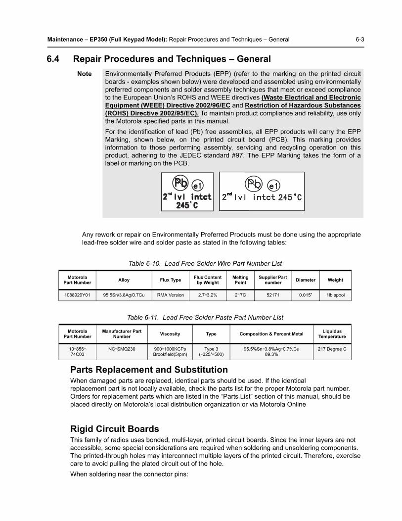
Maintenance – EP350 (Full Keypad Model): Repair Procedures and Techniques – General 6-3
6.4 Repair Procedures and Techniques – General
Any rework or repair on Environmentally Preferred Products must be done using the appropriate lead-free solder wire and solder paste as stated in the following tables:
Parts Replacement and SubstitutionWhen damaged parts are replaced, identical parts should be used. If the identicalreplacement part is not locally available, check the parts list for the proper Motorola part number.Orders for replacement parts which are listed in the “Parts List” section of this manual, should beplaced directly on Motorola’s local distribution organization or via Motorola Online
Rigid Circuit BoardsThis family of radios uses bonded, multi-layer, printed circuit boards. Since the inner layers are not accessible, some special considerations are required when soldering and unsoldering components. The printed-through holes may interconnect multiple layers of the printed circuit. Therefore, exercise care to avoid pulling the plated circuit out of the hole.When soldering near the connector pins:
Note Environmentally Preferred Products (EPP) (refer to the marking on the printed circuitboards - examples shown below) were developed and assembled using environmentallypreferred components and solder assembly techniques that meet or exceed complianceto the European Union’s ROHS and WEEE directives (Waste Electrical and ElectronicEquipment (WEEE) Directive 2002/96/EC and Restriction of Hazardous Substances(ROHS) Directive 2002/95/EC). To maintain product compliance and reliability, use onlythe Motorola specified parts in this manual.For the identification of lead (Pb) free assemblies, all EPP products will carry the EPPMarking, shown below, on the printed circuit board (PCB). This marking providesinformation to those performing assembly, servicing and recycling operation on thisproduct, adhering to the JEDEC standard #97. The EPP Marking takes the form of alabel or marking on the PCB.
Table 6-10. Lead Free Solder Wire Part Number List
Motorola Part Number Alloy Flux Type Flux Content
by WeightMelting Point
Supplier Part number Diameter Weight
1088929Y01 95.5Sn/3.8Ag/0.7Cu RMA Version 2.7-3.2% 217C 52171 0.015” 1lb spool
Table 6-11. Lead Free Solder Paste Part Number List
Motorola Part Number
Manufacturer Part Number Viscosity Type Composition & Percent Metal Liquidus
Temperature
10-856-74C03
NC-SMQ230 900-1000KCPs Brookfield(5rpm)
Type 3(-325/+500)
95.5%Sn-3.8%Ag-0.7%Cu89.3%
217 Degree C
6-4 Maintenance – EP350 (Full Keypad Model): Repair Procedures and Techniques – General
• Avoid accidentally getting solder in the connector. • Be careful not to form solder bridges between the connector pins. • Examine your work closely for shorts due to solder bridges.
Chip Components
Use the RLN4062 Hot-Air Repair Station for chip component replacement. Adjust the temperature control to 390 °C (735 °F), and adjust the airflow to a minimum setting. Airflow can vary due to component density.
• To remove a chip component:
1. Use a hot-air hand piece and position the nozzle of the hand piece approximately 0.3 cm (1/8") above the component to be removed.
2. Begin applying the hot air. Once thde solder reflows, remove the component using a pair of tweezers.
3. Using a solder wick and a soldering iron or a power desoldering station, remove the excess solder from the pads.
• To replace a chip component using a soldering iron:
1. Select the appropriate micro-tipped soldering iron and apply fresh solder to one of the solder pads.
2. Using a pair of tweezers, position the new chip component in place while heating the fresh solder.
3. Once solder wicks onto the new component, remove the heat from the solder. 4. Heat the remaining pad with the soldering iron and apply solder until it wicks to the
component. If necessary, touch up the first side. All solder joints should be smooth and shiny.
• To replace a chip component using hot air:
1. Use the hot-air hand piece and reflow the solder on the solder pads to smooth it. 2. Apply a drop of solder paste flux to each pad. 3. Using a pair of tweezers, position the new component in place. 4. Position the hot-air hand piece approximately 0.3 cm (1/8") above the component and
begin applying heat. 5. Once the solder wicks to the component, remove the heat and inspect the repair. All
joints should be smooth and shiny.
Maintenance – EP350 (Full Keypad Model): Repair Procedures and Techniques – General 6-5
Shields
Removing and replacing shields is recommended to be done with the Air Blower, BOSCH GHG 603 or equivalent.
• To remove the shield:
1. Place the circuit board in the circuit board holder. 2. Add solder paste flux around the base of the shield. 3. Position the heat-focus head onto the shield. 4. Turn on the heater and wait until the shield lifts off the circuit board. 5. Once the shield is off, turn off the heat, and grab the part with a pair of tweezers.6. Remove the circuit board from the circuit board holder.
• To replace the shield:
1. Add solder to the shield if necessary, using a micro-tipped soldering iron. 2. Next, rub the soldering iron tip along the edge of the shield to smooth out any excess
solder. Use solder wick and a soldering iron to remove excess solder from the solder pads on the circuit board.
3. Place the circuit board back in the circuit board holder. 4. Place the shield on the circuit board using a pair of tweezers. 5. Position the heat-focus head over the shield. 6. Turn on the heater and wait for the solder to reflow.7. Once complete, turn off the heat, raise the heat-focus head and wait approximately one
minute for the part to cool. 8. Remove the circuit board and inspect the repair. No cleaning should be necessary.
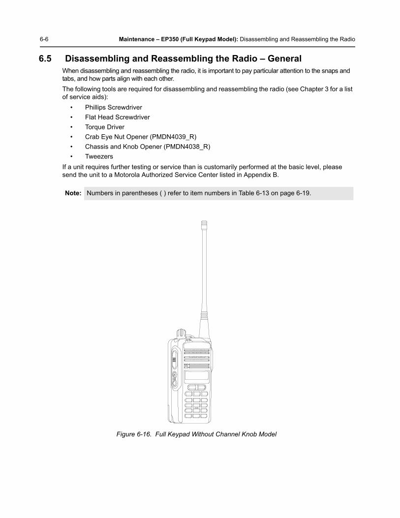
6-6 Maintenance – EP350 (Full Keypad Model): Disassembling and Reassembling the Radio
6.5 Disassembling and Reassembling the Radio – GeneralWhen disassembling and reassembling the radio, it is important to pay particular attention to the snaps and tabs, and how parts align with each other.The following tools are required for disassembling and reassembling the radio (see Chapter 3 for a list of service aids):
• Phillips Screwdriver• Flat Head Screwdriver• Torque Driver• Crab Eye Nut Opener (PMDN4039_R)• Chassis and Knob Opener (PMDN4038_R)• Tweezers
If a unit requires further testing or service than is customarily performed at the basic level, please send the unit to a Motorola Authorized Service Center listed in Appendix B.
Note: Numbers in parentheses ( ) refer to item numbers in Table 6-13 on page 6-19.
Figure 6-16. Full Keypad Without Channel Knob Model

Maintenance – EP350 (Full Keypad Model): Disassembling and Reassembling the Radio 6-7
6.5.1 Radio Disassembly – Detailed
6.5.1.1 Front Housing From Chassis Disassembly1. Turn off the radio.2. Remove the Battery (29):
a. Release the battery latch by moving it into the unlock position.
b. Slide the Battery downwards.
c. Remove the Battery from the radio.
3. Remove the Antenna (21) by turning it counterclockwise.4. Remove the Volume Knob (7) from its shaft using the Chassis and Knob Opener.
(Refer Figure 6-18).
Figure 6-17. Battery and Antenna Removal
Figure 6-18. Knob Removal
AntennaBelt Clip
Battery
Battery Latch
Volume Knob
Chassis and Knob Opener
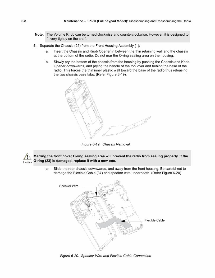
6-8 Maintenance – EP350 (Full Keypad Model): Disassembling and Reassembling the Radio
5. Separate the Chassis (25) from the Front Housing Assembly (1):a. Insert the Chassis and Knob Opener in between the thin retaining wall and the chassis
at the bottom of the radio. Do not mar the O-ring sealing area on the housing.
b. Slowly pry the bottom of the chassis from the housing by pushing the Chassis and Knob Opener downwards, and prying the handle of the tool over and behind the base of the radio. This forces the thin inner plastic wall toward the base of the radio thus releasing the two chassis base tabs. (Refer Figure 6-19).
Figure 6-19. Chassis Removal
c. Slide the rear chassis downwards, and away from the front housing. Be careful not to damage the Flexible Cable (37) and speaker wire underneath. (Refer Figure 6-20).
Note: The Volume Knob can be turned clockwise and counterclockwise. However, it is designed tofit very tightly on the shaft.
Marring the front cover O-ring sealing area will prevent the radio from sealing properly. If the O-ring (23) is damaged, replace it with a new one.
Figure 6-20. Speaker Wire and Flexible Cable Connection
Speaker Wire
Flexible Cable

Maintenance – EP350 (Full Keypad Model): Disassembling and Reassembling the Radio 6-9
d. Remove the speaker wire connector connecting the main circuit board and the internal speaker on the front housing with the tweezers. (Refer Figure 6-21)
e. Lay the front housing down. Rotate the chassis sideways from the Front Housing Assembly (1) and lay it down.
f. Push the latches on the Front Circuit Board (39) sideways to the right to release the flexible cable from the connector. (Refer Figure 6-22).
Note: The speaker wire and flexible cable connector connecting the Front Housing Assembly (1)and the Chassis (25) prevent the two units from being completely separated
Figure 6-21. Speaker Wire Removal
Figure 6-22. Unlatch the Flexible Cable
Speaker Connector
Latches
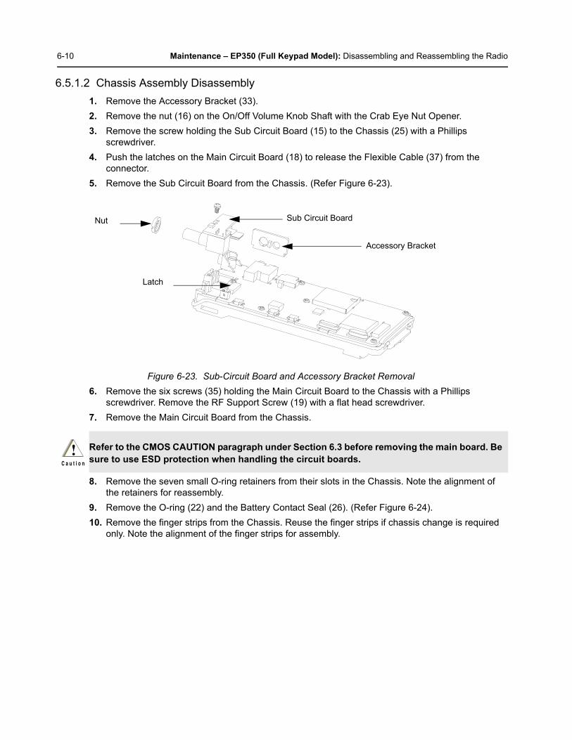
6-10 Maintenance – EP350 (Full Keypad Model): Disassembling and Reassembling the Radio
6.5.1.2 Chassis Assembly Disassembly1. Remove the Accessory Bracket (33).2. Remove the nut (16) on the On/Off Volume Knob Shaft with the Crab Eye Nut Opener.3. Remove the screw holding the Sub Circuit Board (15) to the Chassis (25) with a Phillips
screwdriver. 4. Push the latches on the Main Circuit Board (18) to release the Flexible Cable (37) from the
connector.5. Remove the Sub Circuit Board from the Chassis. (Refer Figure 6-23).
6. Remove the six screws (35) holding the Main Circuit Board to the Chassis with a Phillips screwdriver. Remove the RF Support Screw (19) with a flat head screwdriver.
7. Remove the Main Circuit Board from the Chassis.
8. Remove the seven small O-ring retainers from their slots in the Chassis. Note the alignment of the retainers for reassembly.
9. Remove the O-ring (22) and the Battery Contact Seal (26). (Refer Figure 6-24).10. Remove the finger strips from the Chassis. Reuse the finger strips if chassis change is required
only. Note the alignment of the finger strips for assembly.
Figure 6-23. Sub-Circuit Board and Accessory Bracket Removal
Refer to the CMOS CAUTION paragraph under Section 6.3 before removing the main board. Be sure to use ESD protection when handling the circuit boards.
Nut
Accessory Bracket
Sub Circuit Board
Latch
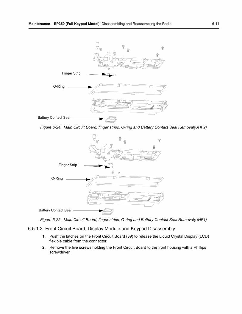
Maintenance – EP350 (Full Keypad Model): Disassembling and Reassembling the Radio 6-11
6.5.1.3 Front Circuit Board, Display Module and Keypad Disassembly1. Push the latches on the Front Circuit Board (39) to release the Liquid Crystal Display (LCD)
flexible cable from the connector.2. Remove the five screws holding the Front Circuit Board to the front housing with a Phillips
screwdriver.
Figure 6-24. Main Circuit Board, finger strips, O-ring and Battery Contact Seal Removal(UHF2)
Figure 6-25. Main Circuit Board, finger strips, O-ring and Battery Contact Seal Removal(UHF1)
O-Ring
Battery Contact Seal
Finger Strip
O-Ring
Battery Contact Seal
Finger Strip
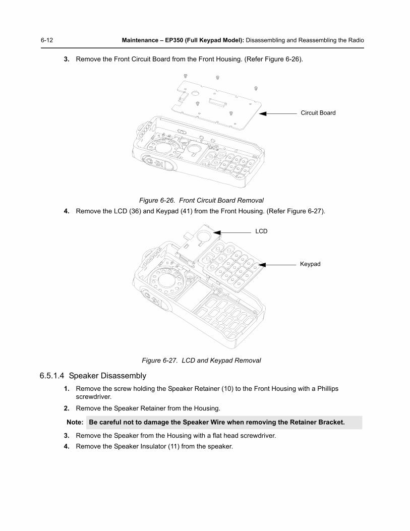
6-12 Maintenance – EP350 (Full Keypad Model): Disassembling and Reassembling the Radio
3. Remove the Front Circuit Board from the Front Housing. (Refer Figure 6-26).
4. Remove the LCD (36) and Keypad (41) from the Front Housing. (Refer Figure 6-27).
6.5.1.4 Speaker Disassembly1. Remove the screw holding the Speaker Retainer (10) to the Front Housing with a Phillips
screwdriver.
2. Remove the Speaker Retainer from the Housing.
3. Remove the Speaker from the Housing with a flat head screwdriver.4. Remove the Speaker Insulator (11) from the speaker.
Figure 6-26. Front Circuit Board Removal
Figure 6-27. LCD and Keypad Removal
Note: Be careful not to damage the Speaker Wire when removing the Retainer Bracket.
Circuit Board
Keypad
LCD

Maintenance – EP350 (Full Keypad Model): Disassembling and Reassembling the Radio 6-13
5. Remove the Speaker Felt (8) from the grille area (Refer Figure 6-28).
6.5.2 Radio Reassembly – Detailed
6.5.2.1 Speaker Reassembly1. Place the Speaker Felt (8) onto the grille area.2. Align the speaker wire at three o'clock position and push down the speaker until fully adhere onto
the front housing.3. Align the Speaker Insulator (11) at twelve o'clock position and push down until fully adhere onto
the speaker.4. Install the Speaker Retainer (10).5. Tighten the Speaker Retainer to the housing with a Phillips screw torque to (Refer Table 6-12 on
page 6-17 for torque in other units).
Figure 6-28. Speaker Removal
Figure 6-29. Speaker Reassembly
Speaker Retainer
Speaker
Speaker Felt
Speaker Insulator
Speaker Retainer
Speaker
Speaker Felt
Speaker Insulator
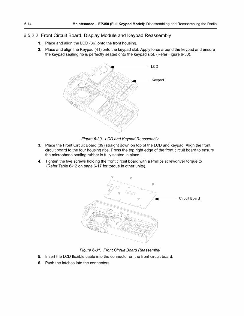
6-14 Maintenance – EP350 (Full Keypad Model): Disassembling and Reassembling the Radio
6.5.2.2 Front Circuit Board, Display Module and Keypad Reassembly1. Place and align the LCD (36) onto the front housing.2. Place and align the Keypad (41) onto the keypad slot. Apply force around the keypad and ensure
the keypad sealing rib is perfectly seated onto the keypad slot. (Refer Figure 6-30).
3. Place the Front Circuit Board (39) straight down on top of the LCD and keypad. Align the front circuit board to the four housing ribs. Press the top right edge of the front circuit board to ensure the microphone sealing rubber is fully seated in place.
4. Tighten the five screws holding the front circuit board with a Phillips screwdriver torque to (Refer Table 6-12 on page 6-17 for torque in other units).
5. Insert the LCD flexible cable into the connector on the front circuit board.6. Push the latches into the connectors.
Figure 6-30. LCD and Keypad Reassembly
Figure 6-31. Front Circuit Board Reassembly
LCD
Keypad
Circuit Board

Maintenance – EP350 (Full Keypad Model): Disassembling and Reassembling the Radio 6-15
6.5.2.3 Chassis Assembly Reassembly1. Fit the Battery Contact Seal (26) onto the battery contact slot.2. Align and assemble the finger strips for assembly. 3. Fit the main O-ring (22) onto the chassis as follow:
a. Ensure that the main O-ring is not twisted. Untangle to original form if necessary.
b. Secure A into the bottom two notches on the chassis. (Refer Figure 6-32).
c. Fit the bottom section of the main O-ring around the bottom two grooves.
d. Insert B into the top two catches on the chassis.
e. Fit the top section of the main O-ring around the top two corners of the chassis.
f. Secure C into the remaining three notches on the chassis.
4. Place the main circuit board straight down on top of the chassis.
5. Tighten the six screws holding the main circuit board with a Phillips screwdriver torque to (Refer Table 6-12 on page 6-17 for torque in other units).
6. Tighten the RF Support Screw (19) with a flat head screw torque to (Refer Table 6-12 on page 6-17 for torque in other units)..
Note: Make sure the battery contact seal protrudes through the chassis and is not squeezed under the chassis. Ensure the O-ring is also not squeezed under main circuit board.
Figure 6-32. Main Circuit Board, finger strips, O-ring and Battery Contact Seal Reassembly(UHF2)
AB
C
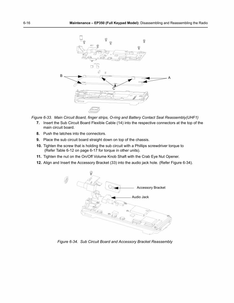
6-16 Maintenance – EP350 (Full Keypad Model): Disassembling and Reassembling the Radio
7. Insert the Sub Circuit Board Flexible Cable (14) into the respective connectors at the top of the main circuit board.
8. Push the latches into the connectors.9. Place the sub circuit board straight down on top of the chassis. 10. Tighten the screw that is holding the sub circuit with a Phillips screwdriver torque to
(Refer Table 6-12 on page 6-17 for torque in other units).11. Tighten the nut on the On/Off Volume Knob Shaft with the Crab Eye Nut Opener.12. Align and Insert the Accessory Bracket (33) into the audio jack hole. (Refer Figure 6-34).
Figure 6-33. Main Circuit Board, finger strips, O-ring and Battery Contact Seal Reassembly(UHF1)
Figure 6-34. Sub Circuit Board and Accessory Bracket Reassembly
AB
C
Accessory Bracket
Audio Jack
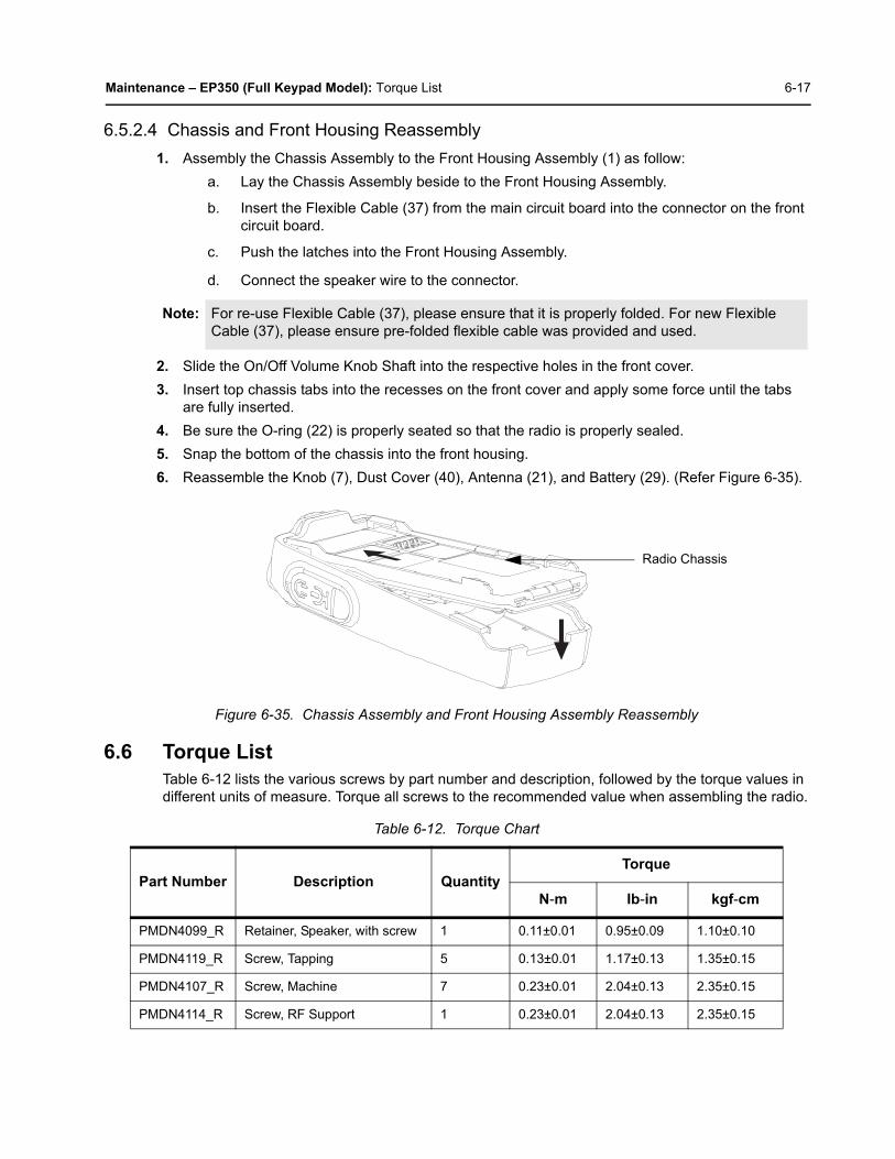
Maintenance – EP350 (Full Keypad Model): Torque List 6-17
6.5.2.4 Chassis and Front Housing Reassembly1. Assembly the Chassis Assembly to the Front Housing Assembly (1) as follow:
a. Lay the Chassis Assembly beside to the Front Housing Assembly.
b. Insert the Flexible Cable (37) from the main circuit board into the connector on the front circuit board.
c. Push the latches into the Front Housing Assembly.
d. Connect the speaker wire to the connector.
2. Slide the On/Off Volume Knob Shaft into the respective holes in the front cover.3. Insert top chassis tabs into the recesses on the front cover and apply some force until the tabs
are fully inserted.4. Be sure the O-ring (22) is properly seated so that the radio is properly sealed.5. Snap the bottom of the chassis into the front housing.6. Reassemble the Knob (7), Dust Cover (40), Antenna (21), and Battery (29). (Refer Figure 6-35).
6.6 Torque ListTable 6-12 lists the various screws by part number and description, followed by the torque values in different units of measure. Torque all screws to the recommended value when assembling the radio.
Note: For re-use Flexible Cable (37), please ensure that it is properly folded. For new Flexible Cable (37), please ensure pre-folded flexible cable was provided and used.
Figure 6-35. Chassis Assembly and Front Housing Assembly Reassembly
Table 6-12. Torque Chart
Part Number Description QuantityTorque
N-m Ib-in kgf-cm
PMDN4099_R Retainer, Speaker, with screw 1 0.11±0.01 0.95±0.09 1.10±0.10
PMDN4119_R Screw, Tapping 5 0.13±0.01 1.17±0.13 1.35±0.15
PMDN4107_R Screw, Machine 7 0.23±0.01 2.04±0.13 2.35±0.15
PMDN4114_R Screw, RF Support 1 0.23±0.01 2.04±0.13 2.35±0.15
Radio Chassis
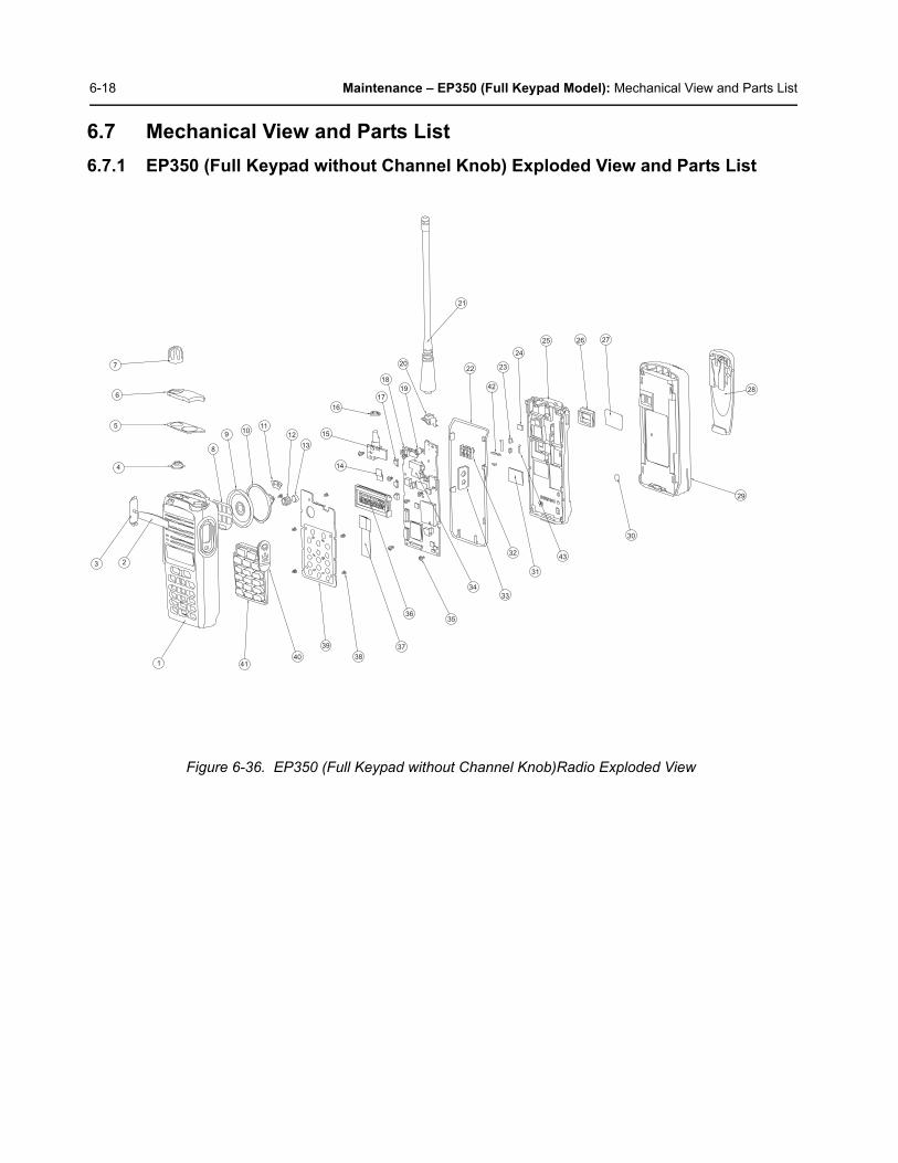
6-18 Maintenance – EP350 (Full Keypad Model): Mechanical View and Parts List
6.7 Mechanical View and Parts List6.7.1 EP350 (Full Keypad without Channel Knob) Exploded View and Parts List
Figure 6-36. EP350 (Full Keypad without Channel Knob)Radio Exploded View
7
6
5
4
8
9 10
11
12
13
14
15
16
17
18
20
21
22
42
23
24
25 26 27
28
29
30
43
31
32
33
34
35 36
37
38
39
40 41 1
2 3
19
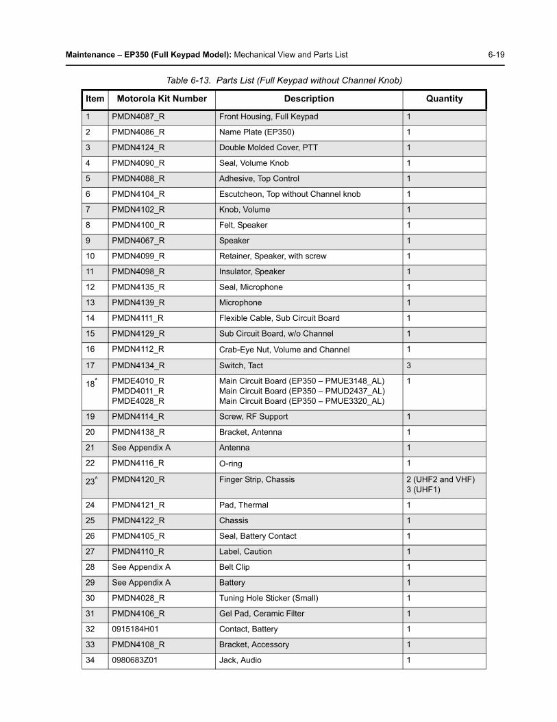
Maintenance – EP350 (Full Keypad Model): Mechanical View and Parts List 6-19
Table 6-13. Parts List (Full Keypad without Channel Knob)
Item Motorola Kit Number Description Quantity
1 PMDN4087_R Front Housing, Full Keypad 1
2 PMDN4086_R Name Plate (EP350) 1
3 PMDN4124_R Double Molded Cover, PTT 1
4 PMDN4090_R Seal, Volume Knob 1
5 PMDN4088_R Adhesive, Top Control 1
6 PMDN4104_R Escutcheon, Top without Channel knob 1
7 PMDN4102_R Knob, Volume 1
8 PMDN4100_R Felt, Speaker 1
9 PMDN4067_R Speaker 1
10 PMDN4099_R Retainer, Speaker, with screw 1
11 PMDN4098_R Insulator, Speaker 1
12 PMDN4135_R Seal, Microphone 1
13 PMDN4139_R Microphone 1
14 PMDN4111_R Flexible Cable, Sub Circuit Board 1
15 PMDN4129_R Sub Circuit Board, w/o Channel 1
16 PMDN4112_R Crab-Eye Nut, Volume and Channel 1
17 PMDN4134_R Switch, Tact 3
18* PMDE4010_RPMDD4011_RPMDE4028_R
Main Circuit Board (EP350 – PMUE3148_AL)Main Circuit Board (EP350 – PMUD2437_AL)Main Circuit Board (EP350 – PMUE3320_AL)
1
19 PMDN4114_R Screw, RF Support 1
20 PMDN4138_R Bracket, Antenna 1
21 See Appendix A Antenna 1
22 PMDN4116_R O-ring 1
23^ PMDN4120_R Finger Strip, Chassis 2 (UHF2 and VHF)3 (UHF1)
24 PMDN4121_R Pad, Thermal 1
25 PMDN4122_R Chassis 1
26 PMDN4105_R Seal, Battery Contact 1
27 PMDN4110_R Label, Caution 1
28 See Appendix A Belt Clip 1
29 See Appendix A Battery 1
30 PMDN4028_R Tuning Hole Sticker (Small) 1
31 PMDN4106_R Gel Pad, Ceramic Filter 1
32 0915184H01 Contact, Battery 1
33 PMDN4108_R Bracket, Accessory 1
34 0980683Z01 Jack, Audio 1
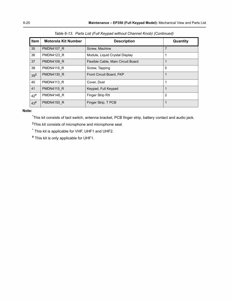
6-20 Maintenance – EP350 (Full Keypad Model): Mechanical View and Parts List
Note: *This kit consists of tact switch, antenna bracket, PCB finger strip, battery contact and audio jack.‡This kit consists of microphone and microphone seal.^ This kit is applicable for VHF, UHF1 and UHF2.# This kit is only applicable for UHF1.
35 PMDN4107_R Screw, Machine 7
36 PMDN4123_R Module, Liquid Crystal Display 1
37 PMDN4109_R Flexible Cable, Main Circuit Board 1
38 PMDN4119_R Screw, Tapping 5
39‡ PMDN4130_R Front Circuit Board, FKP 1
40 PMDN4113_R Cover, Dust 1
41 PMDN4115_R Keypad, Full Keypad 1
42# PMDN4148_R Finger Strip RX 2
43# PMDN4150_R Finger Strip, T PCB 1
Table 6-13. Parts List (Full Keypad without Channel Knob) (Continued)
Item Motorola Kit Number Description Quantity
Chapter 7 Maintenance – EP350 (Limited Keypad Model)
7.1 IntroductionThis section provides details about the following:
• Preventive maintenance (inspection and cleaning)• Safe handling of CMOS and LDMOS devices• Disassembly and reassembly of the radio• Repair procedures and techniques• Mechanical View and Parts List
7.2 Preventive MaintenanceThe radios do not require a scheduled preventive maintenance program; however, periodic visual inspection and cleaning is recommended.
7.2.1 Inspection
Check that the external surfaces of the radio are clean, and that all external controls and switches are functional. It is not recommended to inspect the interior electronic circuitry.
7.2.2 Cleaning Procedures
The following procedures describe the recommended cleaning agents and the methods to be used when cleaning the external and internal surfaces of the radio. External surfaces include the front cover, housing assembly and battery case. These surfaces should be cleaned whenever a periodic visual inspection reveals the presence of smudges, grease, and/or grime.
The only recommended agent for cleaning the external radio surfaces is a 0.5% solution of a mild dishwashing detergent in water. The only factory recommended liquid for cleaning the printed circuit boards and their components is isopropyl alcohol (100% by volume).
Note: Internal surfaces should be cleaned only when the radio is disassembled for service or repair.
The effects of certain chemicals and their vapors can have harmful results on certain plastics. Avoid using aerosol sprays, tuner cleaners, and other chemicals.
7-2 Maintenance – EP350 (Limited Keypad Model): Safe Handling of CMOS and LDMOS Devices
Cleaning External Plastic Surfaces
Apply the 0.5% detergent-water solution sparingly with a stiff, non-metallic, short-bristled brush to work all loose dirt away from the radio. Use a soft, absorbent, lintless cloth or tissue to remove the solution and dry the radio. Make sure that no water remains entrapped near the connectors, cracks, or crevices.
Cleaning Internal Circuit Boards and Components
Isopropyl alcohol (100%) may be applied with a stiff, non-metallic, short-bristled brush to dislodge embedded or caked materials located in hard-to-reach areas. The brush stroke should direct the dislodged material out and away from the inside of the radio. Make sure that controls or tunable components are not soaked with alcohol. Do not use high-pressure air to hasten the drying process since this could cause the liquid to collect in unwanted places. After completing the cleaning process, use a soft, absorbent, lintless cloth to dry the area. Do not brush or apply any isopropyl alcohol to the frame, front cover, or back cover.
7.3 Safe Handling of CMOS and LDMOS DevicesComplementary metal-oxide semiconductor (CMOS) devices are used in this family of radios, and are susceptible to damage by electrostatic or high voltage charges. Damage can be latent, resulting in failures occurring weeks or months later. Therefore, special precautions must be taken to prevent device damage during disassembly, troubleshooting, and repair.
Handling precautions are mandatory for CMOS circuits and are especially important in low humidity conditions. DO NOT attempt to disassemble the radio without first referring to the following CAUTION statement.
Note: Always use a fresh supply of alcohol and a clean container to prevent contamination by dissolved material (from previous usage).
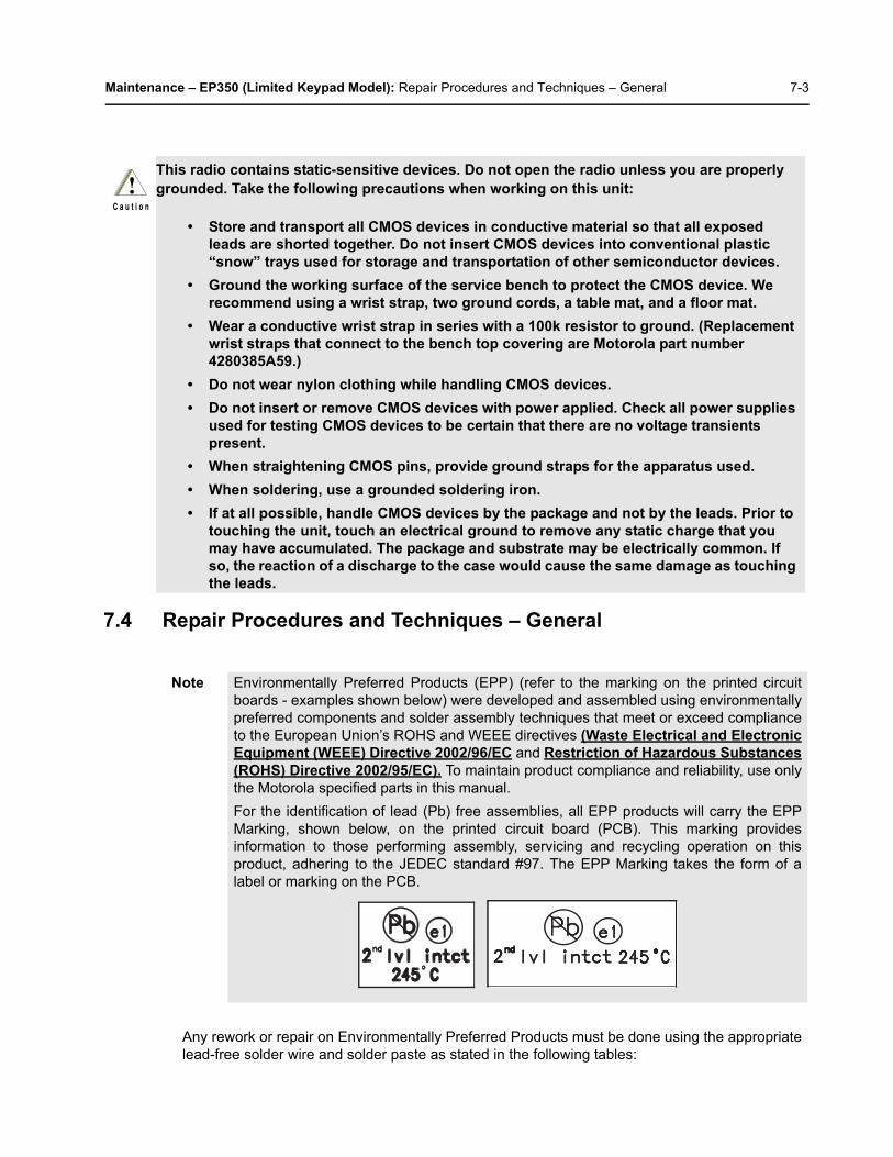
Maintenance – EP350 (Limited Keypad Model): Repair Procedures and Techniques – General 7-3
7.4 Repair Procedures and Techniques – General
Any rework or repair on Environmentally Preferred Products must be done using the appropriate lead-free solder wire and solder paste as stated in the following tables:
This radio contains static-sensitive devices. Do not open the radio unless you are properly grounded. Take the following precautions when working on this unit:
• Store and transport all CMOS devices in conductive material so that all exposed leads are shorted together. Do not insert CMOS devices into conventional plastic “snow” trays used for storage and transportation of other semiconductor devices.
• Ground the working surface of the service bench to protect the CMOS device. We recommend using a wrist strap, two ground cords, a table mat, and a floor mat.
• Wear a conductive wrist strap in series with a 100k resistor to ground. (Replacement wrist straps that connect to the bench top covering are Motorola part number 4280385A59.)
• Do not wear nylon clothing while handling CMOS devices.• Do not insert or remove CMOS devices with power applied. Check all power supplies
used for testing CMOS devices to be certain that there are no voltage transients present.
• When straightening CMOS pins, provide ground straps for the apparatus used.• When soldering, use a grounded soldering iron.• If at all possible, handle CMOS devices by the package and not by the leads. Prior to
touching the unit, touch an electrical ground to remove any static charge that you may have accumulated. The package and substrate may be electrically common. If so, the reaction of a discharge to the case would cause the same damage as touching the leads.
Note Environmentally Preferred Products (EPP) (refer to the marking on the printed circuitboards - examples shown below) were developed and assembled using environmentallypreferred components and solder assembly techniques that meet or exceed complianceto the European Union’s ROHS and WEEE directives (Waste Electrical and ElectronicEquipment (WEEE) Directive 2002/96/EC and Restriction of Hazardous Substances(ROHS) Directive 2002/95/EC). To maintain product compliance and reliability, use onlythe Motorola specified parts in this manual.For the identification of lead (Pb) free assemblies, all EPP products will carry the EPPMarking, shown below, on the printed circuit board (PCB). This marking providesinformation to those performing assembly, servicing and recycling operation on thisproduct, adhering to the JEDEC standard #97. The EPP Marking takes the form of alabel or marking on the PCB.
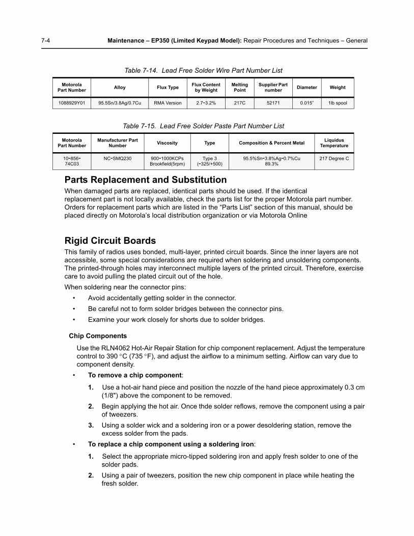
7-4 Maintenance – EP350 (Limited Keypad Model): Repair Procedures and Techniques – General
Parts Replacement and SubstitutionWhen damaged parts are replaced, identical parts should be used. If the identicalreplacement part is not locally available, check the parts list for the proper Motorola part number.Orders for replacement parts which are listed in the “Parts List” section of this manual, should beplaced directly on Motorola’s local distribution organization or via Motorola Online
Rigid Circuit BoardsThis family of radios uses bonded, multi-layer, printed circuit boards. Since the inner layers are not accessible, some special considerations are required when soldering and unsoldering components. The printed-through holes may interconnect multiple layers of the printed circuit. Therefore, exercise care to avoid pulling the plated circuit out of the hole.When soldering near the connector pins:
• Avoid accidentally getting solder in the connector. • Be careful not to form solder bridges between the connector pins. • Examine your work closely for shorts due to solder bridges.
Chip Components
Use the RLN4062 Hot-Air Repair Station for chip component replacement. Adjust the temperature control to 390 °C (735 °F), and adjust the airflow to a minimum setting. Airflow can vary due to component density.
• To remove a chip component:
1. Use a hot-air hand piece and position the nozzle of the hand piece approximately 0.3 cm (1/8") above the component to be removed.
2. Begin applying the hot air. Once thde solder reflows, remove the component using a pair of tweezers.
3. Using a solder wick and a soldering iron or a power desoldering station, remove the excess solder from the pads.
• To replace a chip component using a soldering iron:
1. Select the appropriate micro-tipped soldering iron and apply fresh solder to one of the solder pads.
2. Using a pair of tweezers, position the new chip component in place while heating the fresh solder.
Table 7-14. Lead Free Solder Wire Part Number List
Motorola Part Number Alloy Flux Type Flux Content
by WeightMelting Point
Supplier Part number Diameter Weight
1088929Y01 95.5Sn/3.8Ag/0.7Cu RMA Version 2.7-3.2% 217C 52171 0.015” 1lb spool
Table 7-15. Lead Free Solder Paste Part Number List
Motorola Part Number
Manufacturer Part Number Viscosity Type Composition & Percent Metal Liquidus
Temperature
10-856-74C03
NC-SMQ230 900-1000KCPs Brookfield(5rpm)
Type 3(-325/+500)
95.5%Sn-3.8%Ag-0.7%Cu89.3%
217 Degree C
Maintenance – EP350 (Limited Keypad Model): Repair Procedures and Techniques – General 7-5
3. Once solder wicks onto the new component, remove the heat from the solder. 4. Heat the remaining pad with the soldering iron and apply solder until it wicks to the
component. If necessary, touch up the first side. All solder joints should be smooth and shiny.
• To replace a chip component using hot air:
1. Use the hot-air hand piece and reflow the solder on the solder pads to smooth it. 2. Apply a drop of solder paste flux to each pad. 3. Using a pair of tweezers, position the new component in place. 4. Position the hot-air hand piece approximately 0.3 cm (1/8") above the component and
begin applying heat. 5. Once the solder wicks to the component, remove the heat and inspect the repair. All
joints should be smooth and shiny.
Shields
Removing and replacing shields is recommended to be done with the Air Blower, BOSCH GHG 603 or equivalent.
• To remove the shield:
1. Place the circuit board in the circuit board holder. 2. Add solder paste flux around the base of the shield. 3. Position the heat-focus head onto the shield. 4. Turn on the heater and wait until the shield lifts off the circuit board. 5. Once the shield is off, turn off the heat, and grab the part with a pair of tweezers.6. Remove the circuit board from the circuit board holder.
• To replace the shield:
1. Add solder to the shield if necessary, using a micro-tipped soldering iron. 2. Next, rub the soldering iron tip along the edge of the shield to smooth out any excess
solder. Use solder wick and a soldering iron to remove excess solder from the solder pads on the circuit board.
3. Place the circuit board back in the circuit board holder. 4. Place the shield on the circuit board using a pair of tweezers. 5. Position the heat-focus head over the shield. 6. Turn on the heater and wait for the solder to reflow.7. Once complete, turn off the heat, raise the heat-focus head and wait approximately one
minute for the part to cool. 8. Remove the circuit board and inspect the repair. No cleaning should be necessary.

7-6 Maintenance – EP350 (Limited Keypad Model): Disassembling and Reassembling the Radio
7.5 Disassembling and Reassembling the Radio – GeneralWhen disassembling and reassembling the radio, it is important to pay particular attention to the snaps and tabs, and how parts align with each other.
The following tools are required for disassembling and reassembling the radio (see Chapter 3 for a list of service aids):
• Phillips Screwdriver• Flat Head Screwdriver• Torque Driver• Crab Eye Nut Opener (PMDN4039_R)• Chassis and Knob Opener (PMDN4038_R)• Tweezers
If a unit requires further testing or service than is customarily performed at the basic level, please send the unit to a Motorola Authorized Service Center listed in Appendix B.
Note: Numbers in parentheses ( ) refer to item numbers in Table 7-17 on page 7-19.
Figure 7-37. Limited Keypad Without Channel Knob Model
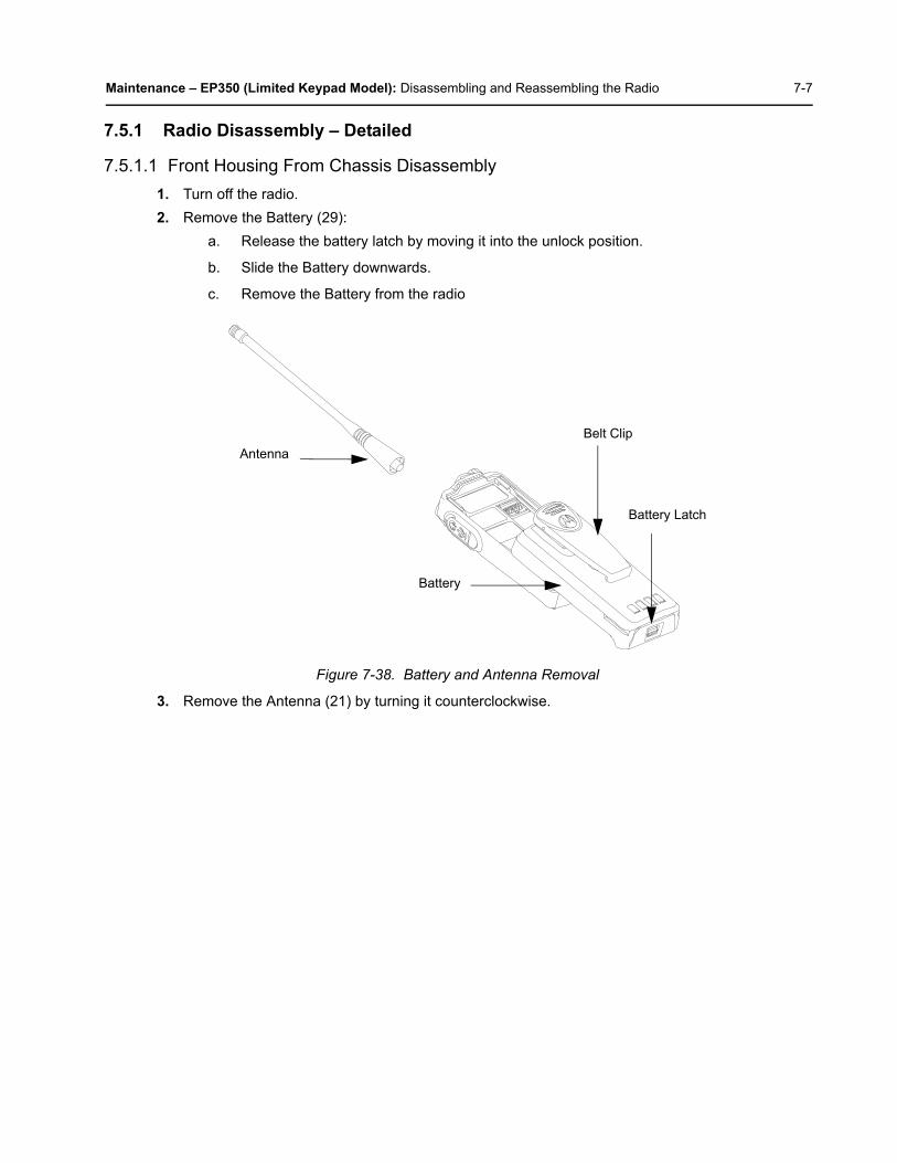
Maintenance – EP350 (Limited Keypad Model): Disassembling and Reassembling the Radio 7-7
7.5.1 Radio Disassembly – Detailed
7.5.1.1 Front Housing From Chassis Disassembly1. Turn off the radio.2. Remove the Battery (29):
a. Release the battery latch by moving it into the unlock position.
b. Slide the Battery downwards.
c. Remove the Battery from the radio
3. Remove the Antenna (21) by turning it counterclockwise.
Figure 7-38. Battery and Antenna Removal
AntennaBelt Clip
Battery
Battery Latch

7-8 Maintenance – EP350 (Limited Keypad Model): Disassembling and Reassembling the Radio
4. Remove the Volume Knob (7) from its shaft using the Chassis and Knob Opener. (Refer Figure 7-39.
5. Separate the Chassis (25) from the Front Housing Assembly (1):a. Insert the Chassis and Knob Opener in between the thin retaining wall and the chassis
at the bottom of the radio. Do not mar the O-ring sealing area on the housing.
b. Slowly pry the bottom of the chassis from the housing by pushing the Chassis and Knob Opener downwards, and prying the handle of the tool over and behind the base of the radio. This forces the thin inner plastic wall toward the base of the radio thus releasing the two chassis base tabs. (Refer Figure 7-40).
Figure 7-40. Chassis Removal
Figure 7-39. Knob Removal
Note: The Volume Knob can be turned clockwise and counterclockwise. However, it is designedto fit very tightly on the shaft.
Marring the front cover O-ring sealing area will prevent the radio from sealing properly. If the O-ring (23) is damaged, replace it with a new one.
Volume Knob
Chassis and Knob Opener

Maintenance – EP350 (Limited Keypad Model): Disassembling and Reassembling the Radio 7-9
c. Slide the rear chassis downwards, and away from the front housing. Be careful not to damage the Flexible Cable (37) and speaker wire underneath. (Refer Figure 7-41).
d. Remove the speaker wire connector connecting the main circuit board and the internal speaker on the front housing with the tweezers. (Refer Figure 7-42).
e. Lay the front housing down. Rotate the chassis sideways from the Front Housing Assembly (1) and lay it down.
Figure 7-41. Speaker Wire and Flexible Cable Connection
Note: The speaker wire and flexible cable connector connecting the Front Housing Assembly (1)and the Chassis (25) prevent the two units from being completely separated
Figure 7-42. Speaker Wire Removal
Speaker Wire
Flexible Cable
Speaker Connector

7-10 Maintenance – EP350 (Limited Keypad Model): Disassembling and Reassembling the Radio
f. Push the latches on the Front Circuit Board (39) sideways to the right to release the flexible cable from the connector. (Refer Figure 7-43).
7.5.1.2 Chassis Assembly Disassembly1. Remove the Accessory Bracket (33).2. Remove the nut (16) on the On Off Volume Knob Shaft with the Crab Eye Nut Opener.3. Remove the screw holding the Sub Circuit Board (15) to the Chassis (25) with a Phillips
screwdriver. 4. Push the latches on the Main Circuit Board (18) to release the Flexible Cable (37) from the
connector.5. Remove the Sub Circuit Board from the Chassis. (Refer Figure 7-44).
6. Remove the six screws (35) holding the Main Circuit Board to the Chassis with a Phillips screwdriver. Remove the RF Support Screw (19) with a flat head screwdriver.
Figure 7-43. Unlatch the Flexible Cable
Figure 7-44. Sub-Circuit Board and Accessory Bracket Removal
Latches
Nut
Accessory Bracket
Sub Circuit Board
Latch
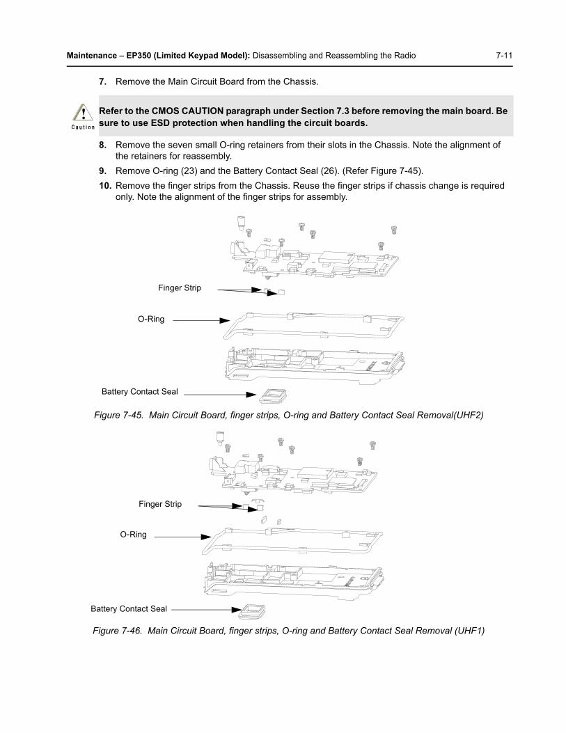
Maintenance – EP350 (Limited Keypad Model): Disassembling and Reassembling the Radio 7-11
7. Remove the Main Circuit Board from the Chassis.
8. Remove the seven small O-ring retainers from their slots in the Chassis. Note the alignment of the retainers for reassembly.
9. Remove O-ring (23) and the Battery Contact Seal (26). (Refer Figure 7-45).10. Remove the finger strips from the Chassis. Reuse the finger strips if chassis change is required
only. Note the alignment of the finger strips for assembly.
Refer to the CMOS CAUTION paragraph under Section 7.3 before removing the main board. Be sure to use ESD protection when handling the circuit boards.
Figure 7-45. Main Circuit Board, finger strips, O-ring and Battery Contact Seal Removal(UHF2)
Figure 7-46. Main Circuit Board, finger strips, O-ring and Battery Contact Seal Removal (UHF1)
O-Ring
Battery Contact Seal
Finger Strip
O-Ring
Battery Contact Seal
Finger Strip
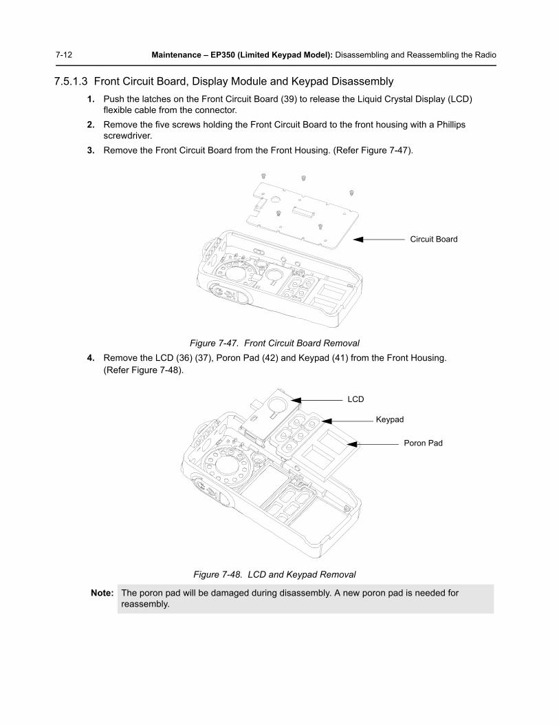
7-12 Maintenance – EP350 (Limited Keypad Model): Disassembling and Reassembling the Radio
7.5.1.3 Front Circuit Board, Display Module and Keypad Disassembly1. Push the latches on the Front Circuit Board (39) to release the Liquid Crystal Display (LCD)
flexible cable from the connector.2. Remove the five screws holding the Front Circuit Board to the front housing with a Phillips
screwdriver. 3. Remove the Front Circuit Board from the Front Housing. (Refer Figure 7-47).
4. Remove the LCD (36) (37), Poron Pad (42) and Keypad (41) from the Front Housing. (Refer Figure 7-48).
Figure 7-47. Front Circuit Board Removal
Figure 7-48. LCD and Keypad Removal
Note: The poron pad will be damaged during disassembly. A new poron pad is needed for reassembly.
Circuit Board
Poron Pad
LCD
Keypad
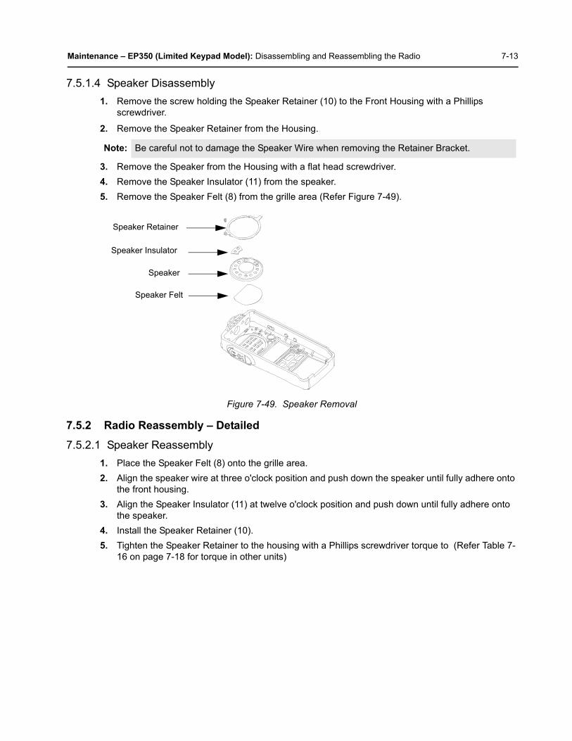
Maintenance – EP350 (Limited Keypad Model): Disassembling and Reassembling the Radio 7-13
7.5.1.4 Speaker Disassembly1. Remove the screw holding the Speaker Retainer (10) to the Front Housing with a Phillips
screwdriver.
2. Remove the Speaker Retainer from the Housing.
3. Remove the Speaker from the Housing with a flat head screwdriver.4. Remove the Speaker Insulator (11) from the speaker.5. Remove the Speaker Felt (8) from the grille area (Refer Figure 7-49).
7.5.2 Radio Reassembly – Detailed
7.5.2.1 Speaker Reassembly1. Place the Speaker Felt (8) onto the grille area.2. Align the speaker wire at three o'clock position and push down the speaker until fully adhere onto
the front housing.3. Align the Speaker Insulator (11) at twelve o'clock position and push down until fully adhere onto
the speaker.4. Install the Speaker Retainer (10).5. Tighten the Speaker Retainer to the housing with a Phillips screwdriver torque to (Refer Table 7-
16 on page 7-18 for torque in other units)
Note: Be careful not to damage the Speaker Wire when removing the Retainer Bracket.
Figure 7-49. Speaker Removal
Speaker Retainer
Speaker
Speaker Felt
Speaker Insulator

7-14 Maintenance – EP350 (Limited Keypad Model): Disassembling and Reassembling the Radio
7.5.2.2 Front Circuit Board, Display Module and Keypad Reassembly1. Place and align the LCD (36) onto the front housing.2. Place and align the Keypad (41) onto the keypad slot. Apply force around the keypad and ensure
the keypad sealing rib is perfectly seated onto the keypad slot. (Refer Figure 7-51).
3. Place the Front Circuit Board (39) straight down on top of the LCD and keypad. Align the front circuit board to the four housing ribs. Press the top right edge of the front circuit board to ensure the microphone sealing rubber is fully seated in place.
4. Tighten the five screws holding the front circuit board with a Phillips screwdriver torque to (Refer Table 7-16 on page 7-18 for torque in other units)
Figure 7-50. Speaker Reassembly
Figure 7-51. LCD and Keypad Reassembly
Speaker Retainer
Speaker
Speaker Felt
Speaker Insulator
LCD
Keypad Poron Pad
Keypad
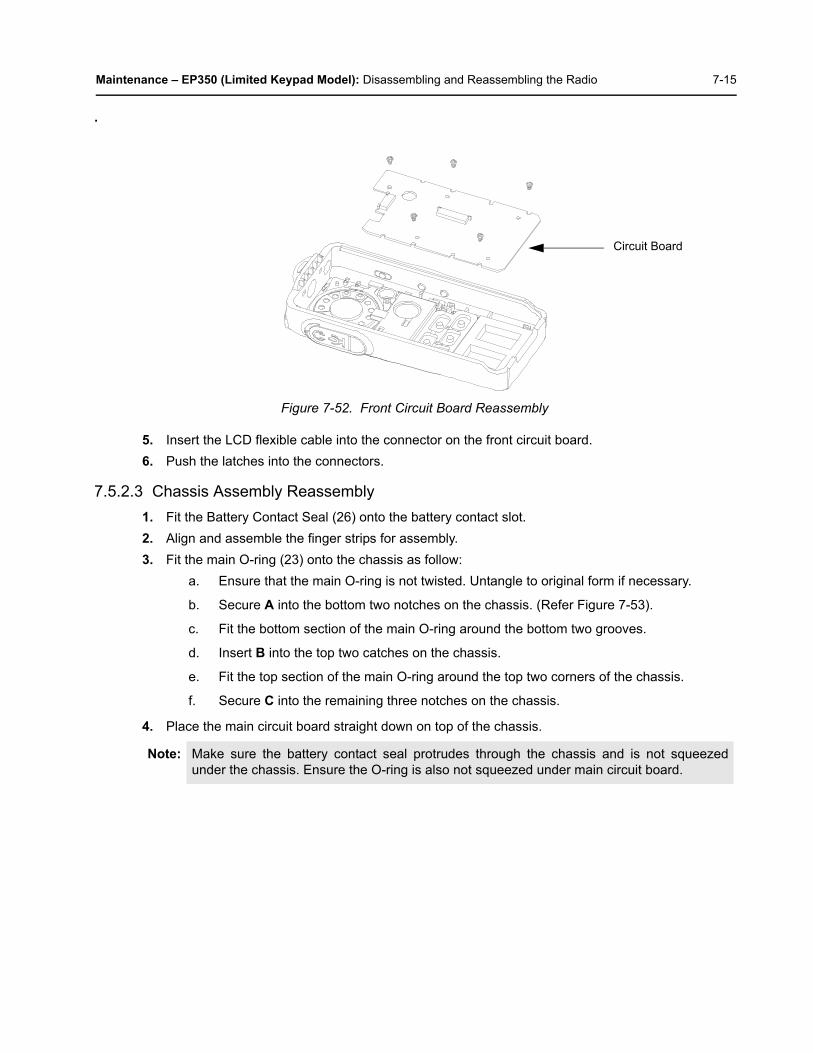
Maintenance – EP350 (Limited Keypad Model): Disassembling and Reassembling the Radio 7-15
.
5. Insert the LCD flexible cable into the connector on the front circuit board.6. Push the latches into the connectors.
7.5.2.3 Chassis Assembly Reassembly1. Fit the Battery Contact Seal (26) onto the battery contact slot.2. Align and assemble the finger strips for assembly.3. Fit the main O-ring (23) onto the chassis as follow:
a. Ensure that the main O-ring is not twisted. Untangle to original form if necessary.
b. Secure A into the bottom two notches on the chassis. (Refer Figure 7-53).
c. Fit the bottom section of the main O-ring around the bottom two grooves.
d. Insert B into the top two catches on the chassis.
e. Fit the top section of the main O-ring around the top two corners of the chassis.
f. Secure C into the remaining three notches on the chassis.
4. Place the main circuit board straight down on top of the chassis.
Figure 7-52. Front Circuit Board Reassembly
Note: Make sure the battery contact seal protrudes through the chassis and is not squeezedunder the chassis. Ensure the O-ring is also not squeezed under main circuit board.
Circuit Board
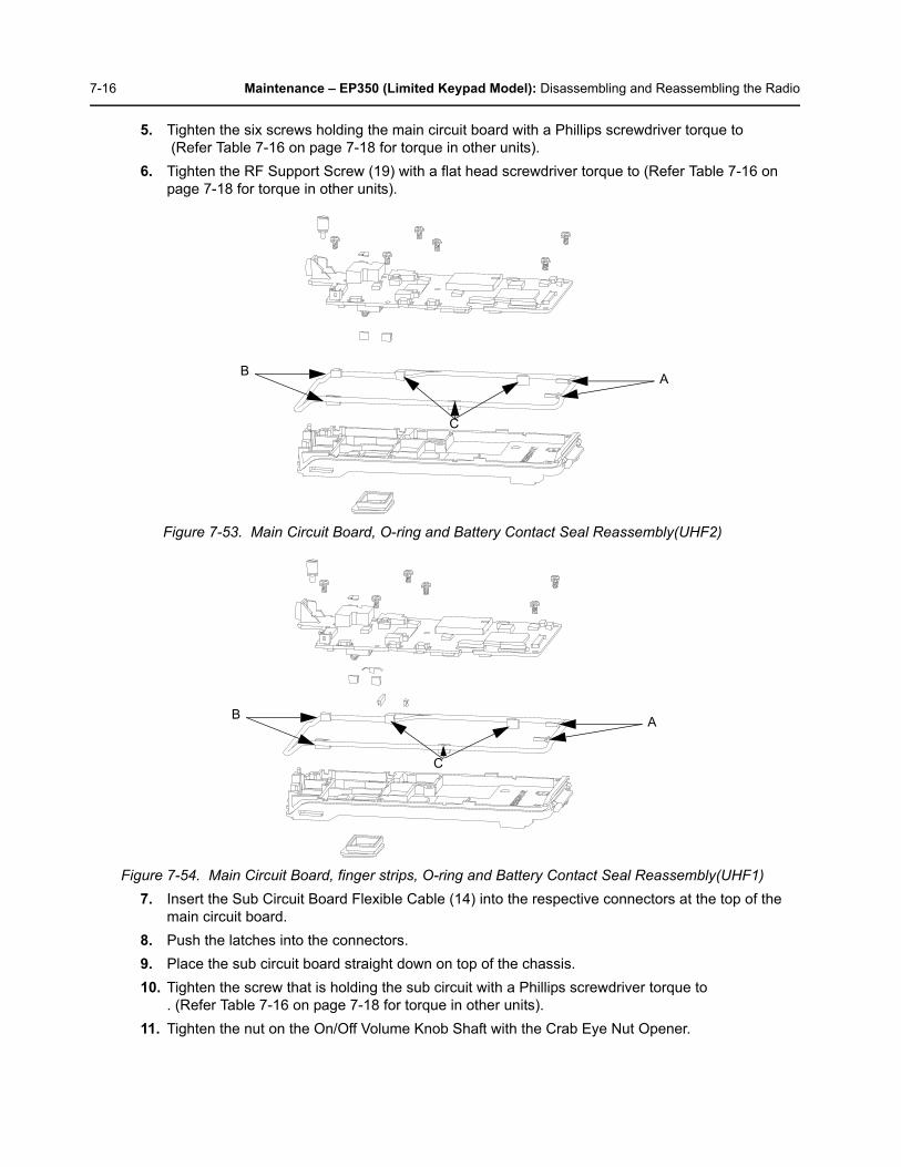
7-16 Maintenance – EP350 (Limited Keypad Model): Disassembling and Reassembling the Radio
5. Tighten the six screws holding the main circuit board with a Phillips screwdriver torque to (Refer Table 7-16 on page 7-18 for torque in other units).
6. Tighten the RF Support Screw (19) with a flat head screwdriver torque to (Refer Table 7-16 on page 7-18 for torque in other units).
7. Insert the Sub Circuit Board Flexible Cable (14) into the respective connectors at the top of the main circuit board.
8. Push the latches into the connectors.9. Place the sub circuit board straight down on top of the chassis. 10. Tighten the screw that is holding the sub circuit with a Phillips screwdriver torque to
. (Refer Table 7-16 on page 7-18 for torque in other units).11. Tighten the nut on the On/Off Volume Knob Shaft with the Crab Eye Nut Opener.
Figure 7-53. Main Circuit Board, O-ring and Battery Contact Seal Reassembly(UHF2)
Figure 7-54. Main Circuit Board, finger strips, O-ring and Battery Contact Seal Reassembly(UHF1)
AB
C
AB
C
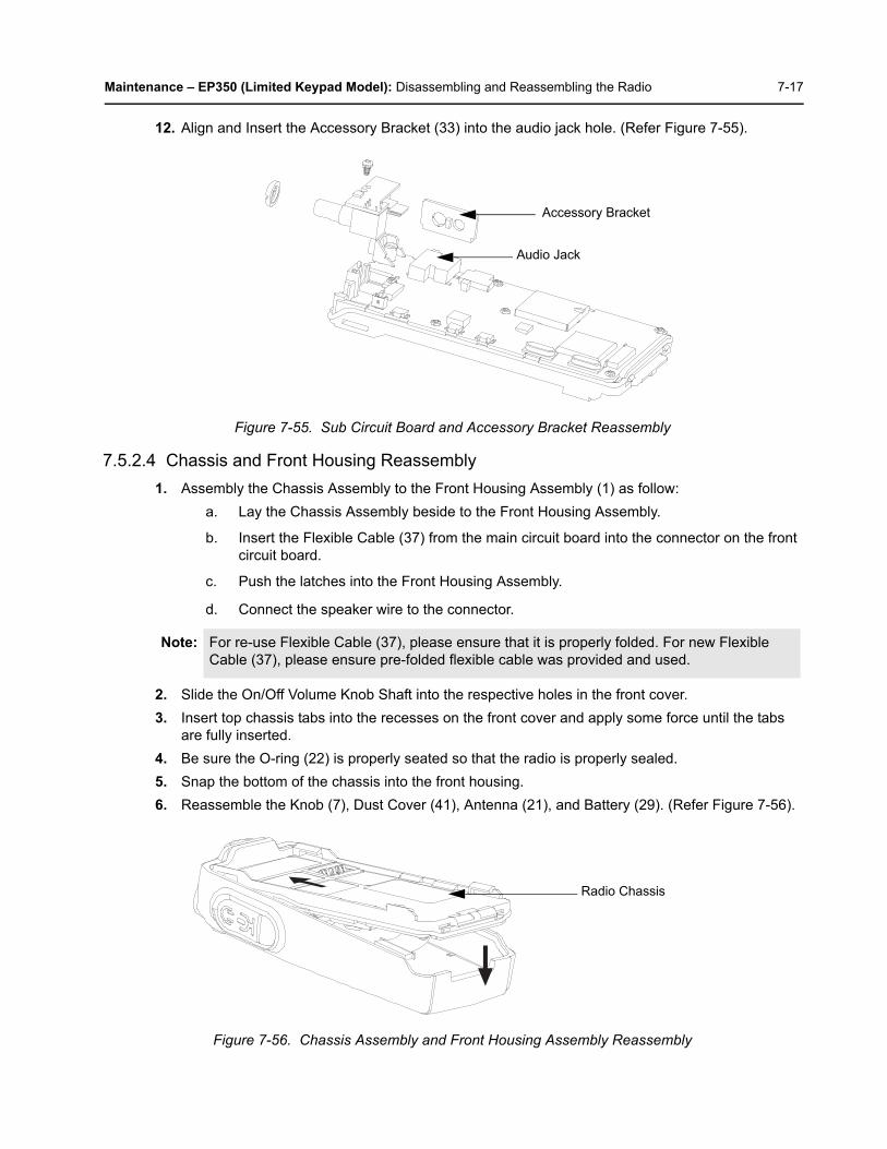
Maintenance – EP350 (Limited Keypad Model): Disassembling and Reassembling the Radio 7-17
12. Align and Insert the Accessory Bracket (33) into the audio jack hole. (Refer Figure 7-55).
7.5.2.4 Chassis and Front Housing Reassembly1. Assembly the Chassis Assembly to the Front Housing Assembly (1) as follow:
a. Lay the Chassis Assembly beside to the Front Housing Assembly.
b. Insert the Flexible Cable (37) from the main circuit board into the connector on the front circuit board.
c. Push the latches into the Front Housing Assembly.
d. Connect the speaker wire to the connector.
2. Slide the On/Off Volume Knob Shaft into the respective holes in the front cover.3. Insert top chassis tabs into the recesses on the front cover and apply some force until the tabs
are fully inserted.4. Be sure the O-ring (22) is properly seated so that the radio is properly sealed.5. Snap the bottom of the chassis into the front housing.6. Reassemble the Knob (7), Dust Cover (41), Antenna (21), and Battery (29). (Refer Figure 7-56).
Figure 7-55. Sub Circuit Board and Accessory Bracket Reassembly
Note: For re-use Flexible Cable (37), please ensure that it is properly folded. For new Flexible Cable (37), please ensure pre-folded flexible cable was provided and used.
Figure 7-56. Chassis Assembly and Front Housing Assembly Reassembly
Accessory Bracket
Audio Jack
Radio Chassis
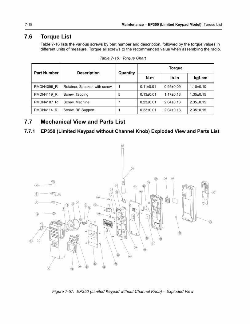
7-18 Maintenance – EP350 (Limited Keypad Model): Torque List
7.6 Torque ListTable 7-16 lists the various screws by part number and description, followed by the torque values in different units of measure. Torque all screws to the recommended value when assembling the radio.
7.7 Mechanical View and Parts List7.7.1 EP350 (Limited Keypad without Channel Knob) Exploded View and Parts List
Figure 7-57. EP350 (Limited Keypad without Channel Knob) – Exploded View
Table 7-16. Torque Chart
Part Number Description QuantityTorque
N-m Ib-in kgf-cm
PMDN4099_R Retainer, Speaker, with screw 1 0.11±0.01 0.95±0.09 1.10±0.10
PMDN4119_R Screw, Tapping 5 0.13±0.01 1.17±0.13 1.35±0.15
PMDN4107_R Screw, Machine 7 0.23±0.01 2.04±0.13 2.35±0.15
PMDN4114_R Screw, RF Support 1 0.23±0.01 2.04±0.13 2.35±0.15
7
6
5
4
3 2
1
8
9 10
11
12
13
14
15
16
17
18
20
19
21
22
43
23
24
25 26 27
28
29
30
44
31
32
33
34
35 36
37
38
39
40 41 42
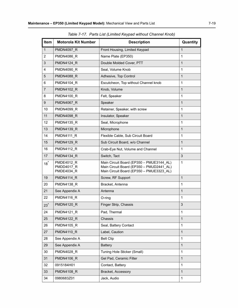
Maintenance – EP350 (Limited Keypad Model): Mechanical View and Parts List 7-19
Table 7-17. Parts List (Limited Keypad without Channel Knob)
Item Motorola Kit Number Description Quantity
1 PMDN4097_R Front Housing, Limited Keypad 1
2 PMDN4086_R Name Plate (EP350) 1
3 PMDN4124_R Double Molded Cover, PTT 1
4 PMDN4090_R Seal, Volume Knob 1
5 PMDN4088_R Adhesive, Top Control 1
6 PMDN4104_R Escutcheon, Top without Channel knob 1
7 PMDN4102_R Knob, Volume 1
8 PMDN4100_R Felt, Speaker 1
9 PMDN4067_R Speaker 1
10 PMDN4099_R Retainer, Speaker, with screw 1
11 PMDN4098_R Insulator, Speaker 1
12 PMDN4135_R Seal, Microphone 1
13 PMDN4139_R Microphone 1
14 PMDN4111_R Flexible Cable, Sub Circuit Board 1
15 PMDN4129_R Sub Circuit Board, w/o Channel 1
16 PMDN4112_R Crab-Eye Nut, Volume and Channel 1
17 PMDN4134_R Switch, Tact 3
18* PMDE4012_RPMDD4017_RPMDE4034_R
Main Circuit Board (EP350 – PMUE3144_AL)Main Circuit Board (EP350 – PMUD2441_AL)Main Circuit Board (EP350 – PMUE3323_AL)
1
19 PMDN4114_R Screw, RF Support 1
20 PMDN4138_R Bracket, Antenna 1
21 See Appendix A Antenna 1
22 PMDN4116_R O-ring 1
23^ PMDN4120_R Finger Strip, Chassis 3
24 PMDN4121_R Pad, Thermal 1
25 PMDN4122_R Chassis 1
26 PMDN4105_R Seal, Battery Contact 1
27 PMDN4110_R Label, Caution 1
28 See Appendix A Belt Clip 1
29 See Appendix A Battery 1
30 PMDN4028_R Tuning Hole Sticker (Small) 1
31 PMDN4106_R Gel Pad, Ceramic Filter 1
32 0915184H01 Contact, Battery 1
33 PMDN4108_R Bracket, Accessory 1
34 0980683Z01 Jack, Audio 1
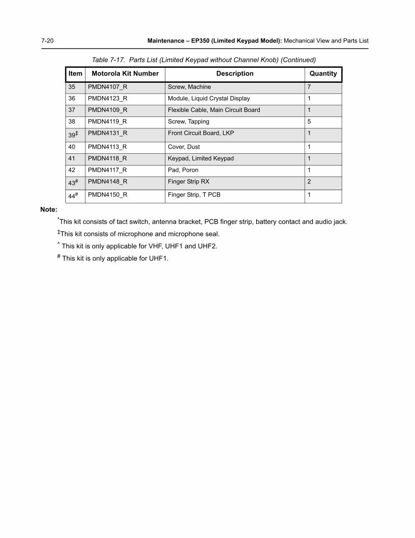
7-20 Maintenance – EP350 (Limited Keypad Model): Mechanical View and Parts List
Note: *This kit consists of tact switch, antenna bracket, PCB finger strip, battery contact and audio jack.‡This kit consists of microphone and microphone seal.^ This kit is only applicable for VHF, UHF1 and UHF2.# This kit is only applicable for UHF1.
35 PMDN4107_R Screw, Machine 7
36 PMDN4123_R Module, Liquid Crystal Display 1
37 PMDN4109_R Flexible Cable, Main Circuit Board 1
38 PMDN4119_R Screw, Tapping 5
39‡ PMDN4131_R Front Circuit Board, LKP 1
40 PMDN4113_R Cover, Dust 1
41 PMDN4118_R Keypad, Limited Keypad 1
42 PMDN4117_R Pad, Poron 1
43# PMDN4148_R Finger Strip RX 2
44# PMDN4150_R Finger Strip, T PCB 1
Table 7-17. Parts List (Limited Keypad without Channel Knob) (Continued)
Item Motorola Kit Number Description Quantity
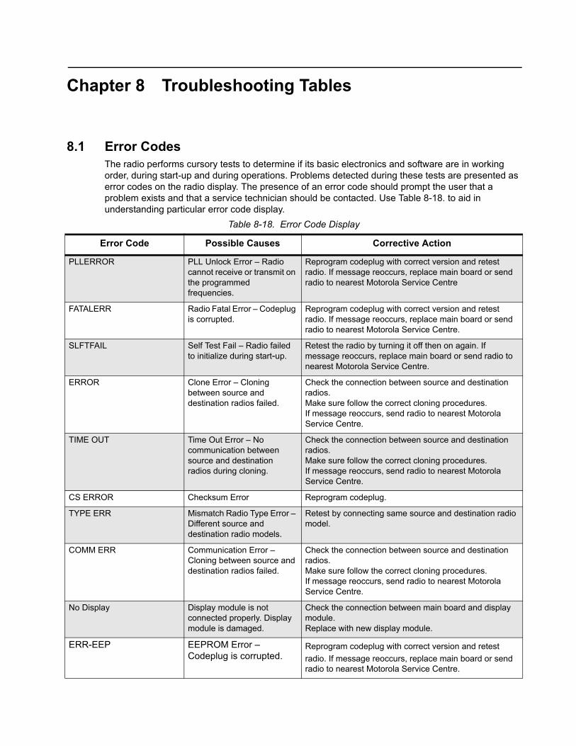
Chapter 8 Troubleshooting Tables
8.1 Error CodesThe radio performs cursory tests to determine if its basic electronics and software are in working order, during start-up and during operations. Problems detected during these tests are presented as error codes on the radio display. The presence of an error code should prompt the user that a problem exists and that a service technician should be contacted. Use Table 8-18. to aid in understanding particular error code display.
Table 8-18. Error Code Display
Error Code Possible Causes Corrective Action
PLLERROR PLL Unlock Error – Radio cannot receive or transmit on the programmed frequencies.
Reprogram codeplug with correct version and retest radio. If message reoccurs, replace main board or send radio to nearest Motorola Service Centre
FATALERR Radio Fatal Error – Codeplug is corrupted.
Reprogram codeplug with correct version and retest radio. If message reoccurs, replace main board or send radio to nearest Motorola Service Centre.
SLFTFAIL Self Test Fail – Radio failed to initialize during start-up.
Retest the radio by turning it off then on again. If message reoccurs, replace main board or send radio to nearest Motorola Service Centre.
ERROR Clone Error – Cloning between source and destination radios failed.
Check the connection between source and destination radios.Make sure follow the correct cloning procedures.If message reoccurs, send radio to nearest Motorola Service Centre.
TIME OUT Time Out Error – No communication between source and destination radios during cloning.
Check the connection between source and destination radios.Make sure follow the correct cloning procedures.If message reoccurs, send radio to nearest Motorola Service Centre.
CS ERROR Checksum Error Reprogram codeplug.
TYPE ERR Mismatch Radio Type Error – Different source and destination radio models.
Retest by connecting same source and destination radio model.
COMM ERR Communication Error – Cloning between source and destination radios failed.
Check the connection between source and destination radios.Make sure follow the correct cloning procedures.If message reoccurs, send radio to nearest Motorola Service Centre.
No Display Display module is not connected properly. Display module is damaged.
Check the connection between main board and display module. Replace with new display module.
ERR-EEP EEPROM Error – Codeplug is corrupted.
Reprogram codeplug with correct version and retestradio. If message reoccurs, replace main board or sendradio to nearest Motorola Service Centre.

8-2 Troubleshooting Tables: Troubleshooting Table for Receiver
8.2 Troubleshooting Table for Receiver Table 8-19. lists the possible causes of, and corrections for, receiver problems.
Symptom Possible Causes Corrective or Test(Measurements at Room Temperature)
Radio Dead; Display Does Not Turn On
1. Dead Battery Replace with charged battery.
2. On/Off Switch Send radio to nearest Motorola Service Centre.
3. Regulators
4. Regulator fault
Radio Dead; Display Turns On
Transceiver Board Send radio to nearest Motorola Service Centre.
No Receive Audio, or Receiver Does Not Unmute
Programming 1. Does the transmitted signal match the receiver configuration (PL, DPL, etc.)?
2. With the monitor function enabled, can the radio be unmuted?
Audio Distorted or Not Loud Enough
Synthesizer Not On Frequency
Send radio to nearest Motorola Service Centre.
Poor RF Sensitivity 1. Synthesizer Not on Frequency
Send radio to nearest Motorola Service Centre.
2. Antenna Switch/Connector
3. Receiver Front End Tuning
Radio Will Not Turn Off Transceiver Board Send radio to nearest Motorola Service Centre.
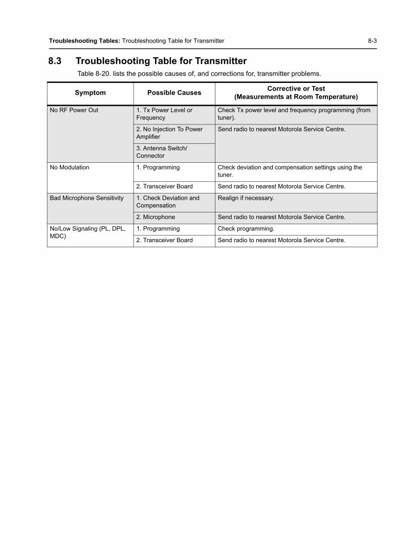
Troubleshooting Tables: Troubleshooting Table for Transmitter 8-3
8.3 Troubleshooting Table for Transmitter Table 8-20. lists the possible causes of, and corrections for, transmitter problems.
Symptom Possible Causes Corrective or Test(Measurements at Room Temperature)
No RF Power Out 1. Tx Power Level or Frequency
Check Tx power level and frequency programming (from tuner).
2. No Injection To Power Amplifier
Send radio to nearest Motorola Service Centre.
3. Antenna Switch/Connector
No Modulation 1. Programming Check deviation and compensation settings using the tuner.
2. Transceiver Board Send radio to nearest Motorola Service Centre.
Bad Microphone Sensitivity 1. Check Deviation and Compensation
Realign if necessary.
2. Microphone Send radio to nearest Motorola Service Centre.
No/Low Signaling (PL, DPL, MDC)
1. Programming Check programming.
2. Transceiver Board Send radio to nearest Motorola Service Centre.

8-4 Troubleshooting Tables: Troubleshooting Table for Transmitter
Notes

Appendix A Accessories
AntennasVHFHAD9338_R VHF Heliflex Antenna (136 – 162 MHz)NAD6502_R VHF Heliflex Antenna (146 – 174 Mhz)NAD6579_ VHF Whip Antenna (148 – 161 MHz)PMAD4012_ VHF Stubby Antenna, 9cm (136 – 155 MHz)PMAD4013_ VHF Stubby Antenna, 9cm (155 – 174 MHz)PMAD4014_ VHF Antenna, 14 cm (136 – 155 MHz)PMAD4049_ VHF Helical Antenna (146 – 174 MHz)
UHFNAE6483_R UHF Whip Antenna, 16.5 cm (403 – 520 MHz)PMAE4002_ UHF Stubby Antenna, 9 cm (403 – 433 MHz)PMAE4003_ UHF Stubby Antenna, 9 cm (430 – 470 MHz)PMAE4006_ UHF Antenna, 9 cm (465 – 495 MHz)PMAE4007_ UHF Antenna, 9 cm (490 – 527 MHz)PMAE4008_ UHF Whip Antenna,13 cm (470 – 530 MHz)PMAE4016_ UHF Whip Antenna (403 – 520 MHz)
Audio Accessories AARLN4885_ Receive Only Earbud for Remote Speaker Microphone Only 3.5 mm AdapterHMN9013_ Lightweight Single Muff Adjustable Headset with Swivel Boom MicrophoneHMN9754_ 2-Wire Earpiece with Microphone and PTT Combined, BeigeRLN5317_ 2-Wire Earpiece with Microphone and PTT Combined, Translucent Tube –
BeigeRLN5318_ 2-Wire Earpiece with Microphone and PTT Combined, Translucent Tube –
BlackRLN4895_ 2-Wire Earpiece with Microphone and PTT Combined, BlackPMMN4008_ Remote Speaker Microphone (MagOne)PMMN4013_ Remote Speaker Microphone with Ear JackPMMN4029_ Remote Speaker MicrophonePMLN4442_ Earbud with In-Line Microphone/PTT/VOX Switch (MagOne)PMLN4443_ Ear Receiver with In-Line Microphone/PTT/VOX Switch (MagOne)PMLN4444_ Earset with Boom Microphone and In-Line PTT/VOX Switch (MagOne)PMLN4445_ Ultra-Light Headset with Boom Microphone and In-Line PTT/VOX Switch
(MagOne)PMLN4620_ D-Shell Earpiece (Remote Speaker Microphone Only) 3.5 mm AdapterPMLN5001_ D-Style Earpiece with Microphone/PTT
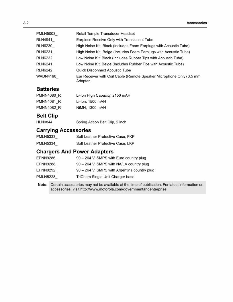
A-2 Accessories
PMLN5003_ Retail Temple Transducer HeadsetRLN4941_ Earpiece Receive Only with Translucent TubeRLN6230_ High Noise Kit, Black (Includes Foam Earplugs with Acoustic Tube)RLN6231_ High Noise Kit, Beige (Includes Foam Earplugs with Acoustic Tube)RLN6232_ Low Noise Kit, Black (Includes Rubber Tips with Acoustic Tube)RLN6241_ Low Noise Kit, Beige (Includes Rubber Tips with Acoustic Tube)RLN6242_ Quick Disconnect Acoustic TubeWADN4190_ Ear Receiver with Coil Cable (Remote Speaker Microphone Only) 3.5 mm
Adapter
BatteriesPMNN4080_R Li-Ion High Capacity, 2150 mAHPMNN4081_R Li-Ion, 1500 mAHPMNN4082_R NiMH, 1300 mAH
Belt ClipHLN9844_ Spring Action Belt Clip, 2 inch
Carrying AccessoriesPMLN5333_ Soft Leather Protective Case, FKP
PMLN5334_ Soft Leather Protective Case, LKP
Chargers And Power AdaptersEPNN9286_ 90 – 264 V, SMPS with Euro country plugEPNN9288_ 90 – 264 V, SMPS with NA/LA country plugEPNN9292_ 90 – 264 V, SMPS with Argentina country plug
PMLN5228_ TriChem Single Unit Charger base
Note: Certain accessories may not be available at the time of publication. For latest information on accessories, visit:http://www.motorola.com/governmentandenterprise.
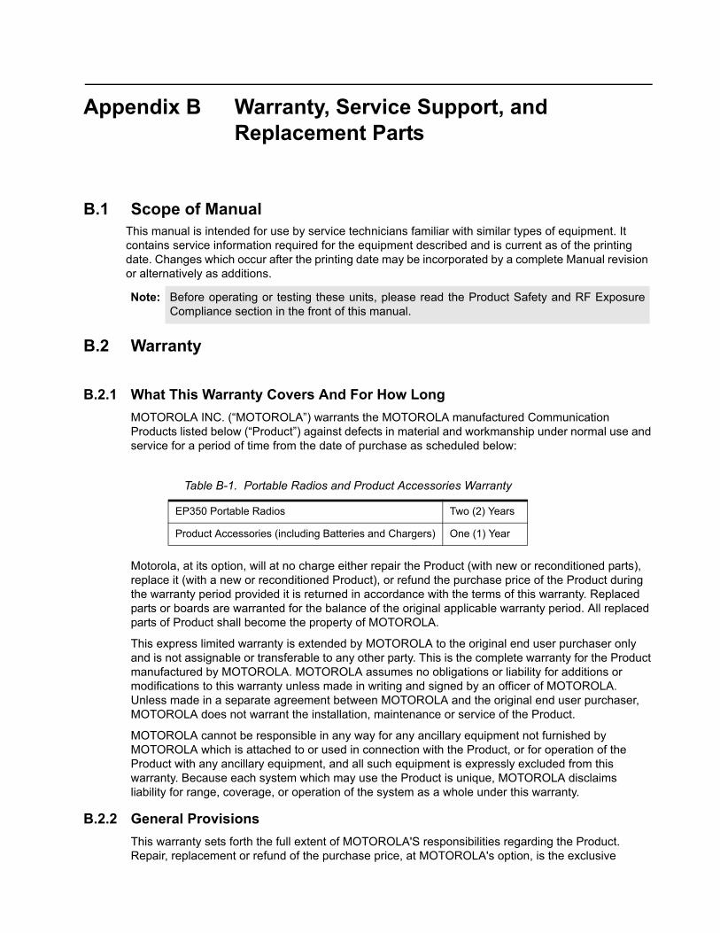
Appendix B Warranty, Service Support, and Replacement Parts
B.1 Scope of ManualThis manual is intended for use by service technicians familiar with similar types of equipment. It contains service information required for the equipment described and is current as of the printing date. Changes which occur after the printing date may be incorporated by a complete Manual revision or alternatively as additions.
B.2 Warranty
B.2.1 What This Warranty Covers And For How LongMOTOROLA INC. (“MOTOROLA”) warrants the MOTOROLA manufactured CommunicationProducts listed below (“Product”) against defects in material and workmanship under normal use andservice for a period of time from the date of purchase as scheduled below:
Motorola, at its option, will at no charge either repair the Product (with new or reconditioned parts),replace it (with a new or reconditioned Product), or refund the purchase price of the Product duringthe warranty period provided it is returned in accordance with the terms of this warranty. Replacedparts or boards are warranted for the balance of the original applicable warranty period. All replacedparts of Product shall become the property of MOTOROLA.
This express limited warranty is extended by MOTOROLA to the original end user purchaser onlyand is not assignable or transferable to any other party. This is the complete warranty for the Productmanufactured by MOTOROLA. MOTOROLA assumes no obligations or liability for additions ormodifications to this warranty unless made in writing and signed by an officer of MOTOROLA. Unless made in a separate agreement between MOTOROLA and the original end user purchaser,MOTOROLA does not warrant the installation, maintenance or service of the Product.
MOTOROLA cannot be responsible in any way for any ancillary equipment not furnished by MOTOROLA which is attached to or used in connection with the Product, or for operation of theProduct with any ancillary equipment, and all such equipment is expressly excluded from this warranty. Because each system which may use the Product is unique, MOTOROLA disclaims liability for range, coverage, or operation of the system as a whole under this warranty.
B.2.2 General ProvisionsThis warranty sets forth the full extent of MOTOROLA'S responsibilities regarding the Product.Repair, replacement or refund of the purchase price, at MOTOROLA's option, is the exclusive
Note: Before operating or testing these units, please read the Product Safety and RF ExposureCompliance section in the front of this manual.
Table B-1. Portable Radios and Product Accessories Warranty
EP350 Portable Radios Two (2) Years
Product Accessories (including Batteries and Chargers) One (1) Year

B-2 Warranty, Service Support, and Replacement Parts: Warranty
remedy. THIS WARRANTY IS GIVEN IN LIEU OF ALL OTHER EXPRESS WARRANTIES. IMPLIEDWARRANTIES, INCLUDING WITHOUT LIMITATION, IMPLIED WARRANTIES OFMERCHANTABILITY AND FITNESS FOR A PARTICULAR PURPOSE, ARE LIMITED TO THEDURATION OF THIS LIMITED WARRANTY. IN NO EVENT SHALL MOTOROLA BE LIABLE FORDAMAGES IN EXCESS OF THE PURCHASE PRICE OF THE PRODUCT, FOR ANY LOSS OFUSE, LOSS OF TIME, INCONVENIENCE, COMMERCIAL LOSS, LOST PROFITS OR SAVINGSOR OTHER INCIDENTAL, SPECIAL OR CONSEQUENTIAL DAMAGES ARISING OUT OF THEUSE OR INABILITY TO USE SUCH PRODUCT, TO THE FULL EXTENT SUCH MAY BEDISCLAIMED BY LAW.
B.2.3 How To Get Warranty ServiceYou must provide proof of purchase (bearing the date of purchase and Product item serial number in order to receive warranty service and, also, deliver or send the Product item, transportation andinsurance prepaid, to an authorized warranty service location. Warranty service will be provided byMotorola through one of its authorized warranty service locations. If you first contact the companywhich sold you the Product, it can facilitate your obtaining warranty service. You can also open aContact Us case on Motorola Online (www.motorola.com/businessonline).
B.2.4 What This Warranty Does Not Cover• Defects or damage resulting from use of the Product in other than its normal and customary• manner.• Defects or damage from misuse, accident, water, or neglect.• Defects or damage from improper testing, operation, maintenance, installation, alteration,• modification, or adjustment.• Breakage or damage to antennas unless caused directly by defects in material workmanship.• A Product subjected to unauthorized Product modifications, disassemblies or repairs (including,• without limitation, the addition to the Product of non-Motorola supplied equipment) which• adversely affect performance of the Product or interfere with Motorola's normal warranty• inspection and testing of the Product to verify any warranty claim.• Product which has had the serial number removed or made illegible.• Rechargeable batteries if:
- any of the seals on the battery enclosure of cells are broken or show evidence of tampering.
- the damage or defect is caused by charging or using the battery in equipment or service other than the Product for which it is specified.
• Freight costs to the repair depot.• A Product which, due to illegal or unauthorized alteration of the software/firmware in the
Product,• does not function in accordance with MOTOROLA’s published specifications or the FCC• type acceptance labeling in effect for the Product at the time the Product was initially distributed• from MOTOROLA.• Scratches or other cosmetic damage to Product surfaces that does not affect the operation of• the Product.• Normal and customary wear and tear.
Warranty, Service Support, and Replacement Parts: Warranty B-3
B.2.5 Patent And Software ProvisionsMOTOROLA will defend, at its own expense, any suit brought against the end user purchaser to theextent that it is based on a claim that the Product or parts infringe a United States patent, andMOTOROLA will pay those costs and damages finally awarded against the end user purchaser inany such suit which are attributable to any such claim, but such defense and payments areconditioned on the following:
• that MOTOROLA will be notified promptly in writing by such purchaser of any notice of suchclaim
• that MOTOROLA will have sole control of the defense of such suit and all negotiations for itssettlement or compromise
• should the Product or parts become, or in MOTOROLA's opinion be likely to become, thesubject of a claim of infringement of a United States patent, that such purchaser will permitMOTOROLA, at its option and expense, either to procure for such purchaser the right tocontinue using the Product or parts or to replace or modify the same so that it becomesnoninfringing or to grant such purchaser a credit for the Product or parts as depreciated andaccept its return. The depreciation will be an equal amount per year over the lifetime of theProduct or parts as established by MOTOROLA.
MOTOROLA will have no liability with respect to any claim of patent infringement which is basedupon the combination of the Product or parts furnished hereunder with software, apparatus ordevices not furnished by MOTOROLA, nor will MOTOROLA have any liability for the use of ancillaryequipment or software not furnished by MOTOROLA which is attached to or used in connection withthe Product. The foregoing states the entire liability of MOTOROLA with respect to infringement ofpatents by the Product or any parts thereof.
Laws in the United States and other countries preserve for MOTOROLA certain exclusive rights forcopyrighted MOTOROLA software such as the exclusive rights to reproduce in copies and distributecopies of such Motorola software. MOTOROLA software may be used in only the Product in whichthe software was originally embodied and such software in such Product may not be replaced,copied, distributed, modified in any way, or used to produce any derivative thereof. No other useincluding, without limitation, alteration, modification, reproduction, distribution, or reverseengineering of such MOTOROLA software or exercise of rights in such MOTOROLA software ispermitted. No license is granted by implication, estoppel or otherwise under MOTOROLA patentrights or copyrights.
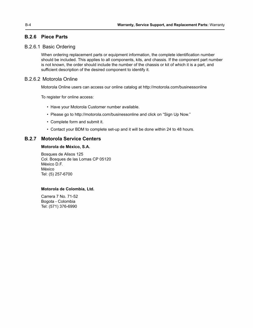
B-4 Warranty, Service Support, and Replacement Parts: Warranty
B.2.6 Piece Parts
B.2.6.1 Basic OrderingWhen ordering replacement parts or equipment information, the complete identification numbershould be included. This applies to all components, kits, and chassis. If the component part numberis not known, the order should include the number of the chassis or kit of which it is a part, andsufficient description of the desired component to identify it.
B.2.6.2 Motorola OnlineMotorola Online users can access our online catalog at http://motorola.com/businessonline
To register for online access:
• Have your Motorola Customer number available.
• Please go to http://motorola.com/businessonline and click on “Sign Up Now.”
• Complete form and submit it.
• Contact your BDM to complete set-up and it will be done within 24 to 48 hours.
B.2.7 Motorola Service CentersMotorola de México, S.A.
Bosques de Alisos 125Col. Bosques de las Lomas CP 05120México D.F.MéxicoTel: (5) 257-6700
Motorola de Colombia, Ltd.
Carrera 7 No. 71-52Bogota - ColombiaTel: (571) 376-6990
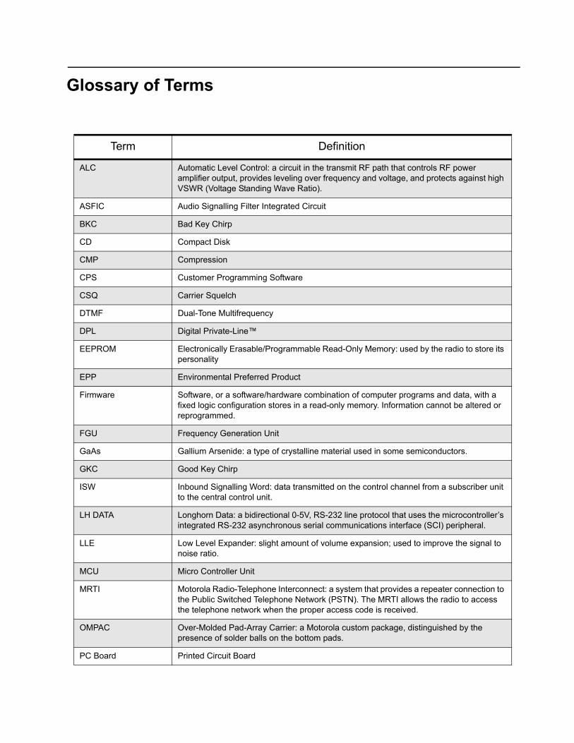
Glossary of Terms
Term Definition
ALC Automatic Level Control: a circuit in the transmit RF path that controls RF power amplifier output, provides leveling over frequency and voltage, and protects against high VSWR (Voltage Standing Wave Ratio).
ASFIC Audio Signalling Filter Integrated Circuit
BKC Bad Key Chirp
CD Compact Disk
CMP Compression
CPS Customer Programming Software
CSQ Carrier Squelch
DTMF Dual-Tone Multifrequency
DPL Digital Private-Line™
EEPROM Electronically Erasable/Programmable Read-Only Memory: used by the radio to store its personality
EPP Environmental Preferred Product
Firmware Software, or a software/hardware combination of computer programs and data, with a fixed logic configuration stores in a read-only memory. Information cannot be altered or reprogrammed.
FGU Frequency Generation Unit
GaAs Gallium Arsenide: a type of crystalline material used in some semiconductors.
GKC Good Key Chirp
ISW Inbound Signalling Word: data transmitted on the control channel from a subscriber unit to the central control unit.
LH DATA Longhorn Data: a bidirectional 0-5V, RS-232 line protocol that uses the microcontroller’s integrated RS-232 asynchronous serial communications interface (SCI) peripheral.
LLE Low Level Expander: slight amount of volume expansion; used to improve the signal to noise ratio.
MCU Micro Controller Unit
MRTI Motorola Radio-Telephone Interconnect: a system that provides a repeater connection to the Public Switched Telephone Network (PSTN). The MRTI allows the radio to access the telephone network when the proper access code is received.
OMPAC Over-Molded Pad-Array Carrier: a Motorola custom package, distinguished by the presence of solder balls on the bottom pads.
PC Board Printed Circuit Board
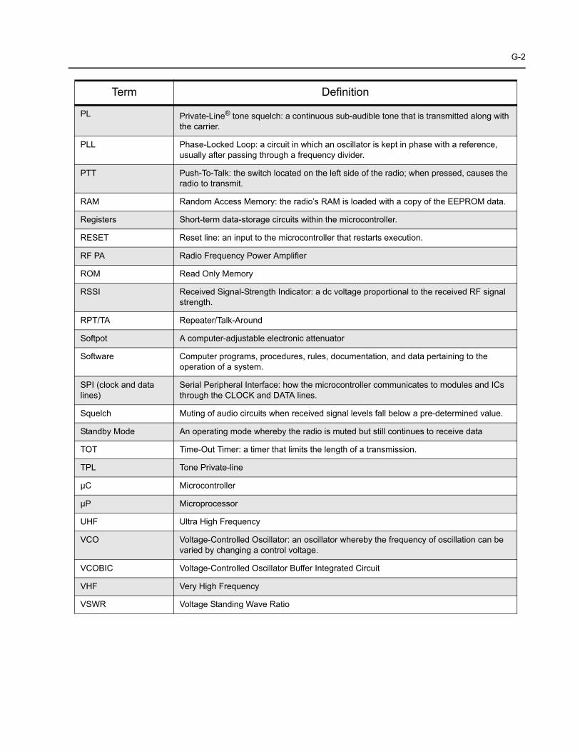
G-2
PL Private-Line® tone squelch: a continuous sub-audible tone that is transmitted along with the carrier.
PLL Phase-Locked Loop: a circuit in which an oscillator is kept in phase with a reference, usually after passing through a frequency divider.
PTT Push-To-Talk: the switch located on the left side of the radio; when pressed, causes the radio to transmit.
RAM Random Access Memory: the radio’s RAM is loaded with a copy of the EEPROM data.
Registers Short-term data-storage circuits within the microcontroller.
RESET Reset line: an input to the microcontroller that restarts execution.
RF PA Radio Frequency Power Amplifier
ROM Read Only Memory
RSSI Received Signal-Strength Indicator: a dc voltage proportional to the received RF signal strength.
RPT/TA Repeater/Talk-Around
Softpot A computer-adjustable electronic attenuator
Software Computer programs, procedures, rules, documentation, and data pertaining to the operation of a system.
SPI (clock and data lines)
Serial Peripheral Interface: how the microcontroller communicates to modules and ICs through the CLOCK and DATA lines.
Squelch Muting of audio circuits when received signal levels fall below a pre-determined value.
Standby Mode An operating mode whereby the radio is muted but still continues to receive data
TOT Time-Out Timer: a timer that limits the length of a transmission.
TPL Tone Private-line
µC Microcontroller
µP Microprocessor
UHF Ultra High Frequency
VCO Voltage-Controlled Oscillator: an oscillator whereby the frequency of oscillation can be varied by changing a control voltage.
VCOBIC Voltage-Controlled Oscillator Buffer Integrated Circuit
VHF Very High Frequency
VSWR Voltage Standing Wave Ratio
Term Definition


© 2009 Motorola Inc. All rights reserved.Motorola Technology Sdn Bhd (Co. No. 455657-H)Plot 2 Bayan Lepas Technoplex Industrial ParkMukim 12 S.W.D11900 Penang, Malaysia
Printed in MalaysiaSeptember 2009
6878419A01-B*6878419A01*


