Embed Size (px)
Citation preview

Capstone Design
14:332:468
A Wearable Pulse Oximeter
Team Members:
Fanpeng Kong
Yubo Qin
Zhengyu Yang
Zhongtian Lin
Faculty Advisor:
Dr. Laleh Najafizadeh
Abstract
In this report, the design and implementation of a low-cost, portable and wearable
pulse oximeter is presented. A pulse oximeter is a non-invasive device capable of
monitoring the blood’s oxygen saturation. It has been widely used in the medical,
fitness and clinical care worlds. A low-cost wearable oximeter can significantly
expand its applicability. The goal of this capstone design project was to design and
build a low-cost wearable pulse oximeter, by using wearable electronics. The system
consists of three main parts: 1) the optical sensor: consisting of the optical
transmitter and receiver for emitting the light and receiving it and filter; 2) the
microcontroller: which receives and processes the signal to display the heart rate and
blood’s oxygen saturation on an LCD display in real time; and 3) mobile phone app
which is designed to receive data wirelessly through Bluetooth. The app can send the
data to another phone via text message, which will make it easy for sending the
heart-rate information to medical doctors in real time, in case of emergency.
I. Introduction
Pulse oximeter is a medical instrument that can detect heart-rate and oxygen
saturation as signatures of our level of health condition. It can be implemented as a
small device, and therefore, has been used widely in different applications. The core
theory behind the pulse oximeter is the variability of the absorption coefficient of
photons going through human tissues at different wavelength. Since people are caring
about the amount of oxygen saturation in our blood, the specific wavelength region
should be settled which is the most sensitive to the oxygen in our blood. In our blood,
oxygenated hemoglobin (Hb) and deoxygenated hemoglobin (deoxy-Hb), which can
be used to measure human blood oxygen level, have stronger absorbers of light with
wavelength in the range of 650 nm-1000 nm (Figure 1). In this wavelength range,
other layers of human body, for instance water and fat, have a very low absorption
coefficient comparing with that of oxygenated hemoglobin and deoxygenated
hemoglobin. Also the good news is that the light absorption of Hb and deoxy-Hb at
the two different wavelengths is different. When the light of around 650 nm
wavelength is emitted to our blood, deoxy-Hb absorbs more than oxy. And vice versa,
if the wavelength is around 1000 nm, a majority portion of photons are absorbed by
Hb. Thus, the ratio of absorption at the two different wavelengths can be used to
determine the oxygen saturation level in the blood. From this discussion, light at
wavelengths of 680 nm and 940 nm are selected in this project.

Figure 1. Absorption Spectrum of Oxy and Deoxy Hemoglobin [1]
The optical sensor is consisted of two different wavelength LEDs and a
photo-detector for receiving the light coming from the finger. In Figure 2, the probe
structure has been shown.
Figure 2. Optical Probe (sensor and detector)
The small amplitude analog current coming from the photo-detector needs to be
amplified by the transimpedance amplifier (TIA) and then processed by a filter. The
microcontroller is one of the most important parts in our design. We programmed it in
order to do the necessary calculations to measure the heart rate and oxygen saturation
level. Also, the Bluetooth communication and LCD display are controlled by our
microcontroller. In the end, the software engineer of the team developed a phone
application which is used to manipulate the whole system. Figure3 shows the design
vision of our target system.
Figure 3. Vision for the target system

The report is organized as follows: the “design approach” section describes the
design of each part of the system. It includes the design of the optical transmitter,
receiver, microcontroller, PCB, Bluetooth communication and development of the
phone application. Next, task distribution, cost comparison and future work for
improving the design are presented. The report is concluded in the Conclusions
section.
II. Design Approach
The project is divided into different blocks as shown in Figure 4.
II.a) Transmitter & Photo-detector
Transmitter is composed by 660 nm and 940 nm LEDs. These two LEDs are
controlled by the microcontroller.
Figure 4. Building Block of Full System
The microcontroller sends two square waves to turn on and off the two LEDs. The
turn on and off timing should be carefully designed because red LED and infrared
LED cannot be turned on at the same time. To control the light intensity, we included
a resistor for each LED. If the light is at high intensity, the photo-detector cannot
work properly. At first, we used bread board to test the microcontroller controlling the
LEDs. In Figure 5, we show the transmitter realized on the breadboard. Because we
needed to put the transmitter on our finger, we needed to implement a compact
transmitter.. Also, this transmitter needs to be smaller for portable applications. After
successful testing of the transmitter on the breadboard, we soldered the LEDs and
resistors on a small board. Figure 6 shows the final transmitter.
On the other side of the finger, there should be a photo-detector which is used to
convert the light signal into electrical signal. The electrical signal’s amplitude,
however, is extremely low. Thus, we need to add an amplifier directly after our
photo-detector to make the signal detectable. This amplifier is named as
transimpedence amplifier (TIA) which can be used not only to amplify but also to
convert the current into voltage. For the photodetector we used IC “OPT101” [2]. The
circuit for this chip can be found in Figure 7. This chip includes both the
photo-detector and TIA together. This IC chip has a 1 MΏ internal resistor and up to
14 KHZ bandwidth. The open loop gain is 90 dB, contributing a very low offset
voltage, around 0.5 V. Also, the minimum operateing power supply is 2.7 V,

consuming a relative low power. Using this IC chip, we do not need to build our own
TIA. This chip can give a good performance output signal.
Figure 5. Bread Board Testing Figure 6. Final Transmitter
Figure 7. Circuit of OPT101 Chip [2]
II-b) Filter
The received signal from OPT101 contains lots of other undesired frequency
components. Thus, we need a band-pass filter to remove the undesired signal, leaving
the signal with the frequency range we need. The receiver filter is set 0.8 HZ to 3 HZ
as the pass band. In addition, the filter should provide some gain added to the signal.
Even though TIA is put behind photo-detector, the overall gain is not enough. In
Figure 8, the circuit schematic is presented.

Figure 8. Whole Receiver Schematic
As presented in the Figure 8, there are two identical filters placed in cascade. Each
filter has the same gain and pass band. Gain is around 20 dB per stage, the pass band
is 0.8 Hz-3Hz. Here we analyze one stage (shown in Figure 9). The band pass filter is
composed by a high pass filter and a low pass filter. The operational amplifier is a
dual amplifier. It should have a large open loop gain. A large open loop gain means
less offset voltage. Thus, the calculated result is more close to the measured result. We
can derive the transfer function for this filter. Equation (1) describes the transfer
function.
Figure 9. First stage filter
Transfer function:
Vout/Vin=
2 3 21 1
2 3 2 3
2 3 2 1 1
(1 )
( )(1 )(1 )
SR R CSC R
R R R R
R SR C SR C
(1)
From this equation, we can directly see the gain equals to:

2 3
2
R RGain
R
(2)
There are two poles in this filter, the first pole cut off frequency is:
1
3 2
1p
R C (3)
The second pole is:
2
1 1
1p
R C (4)
Also, in the numerator we can find the first zero is 0 Hz. The second one is;
2 32
2 3 2
z
R R
R R C
(5)
If we add the second stage together, the gain will be squared. Now, we put the
components value in these equations, and then we get: total gain is 41.7 dB. First pole,
pole1: 0.796 Hz; Second pole, pole2: 3.12 Hz. First zero is at 0 Hz; second zero is at
34.3 Hz. We use Cadence design tool and simulation [3], a standardized industry
software for design and simulating circuits, to design and simulate this whole filter
stage and get the simulation result. The simulation is shown in Figure 10. From the
simulation result, we can see that the pass band is from 0.8-3HZ and the total gain is
around 37.1 dB. These numbers are close to our initial calculation results.
Figure 10. Transfer Function Cadence Simulation Result.
After the simulation, we do the real test. We implemented this circuit on a bread board
and gave a sine signal to the input and used oscilloscope to see the output. We gave
two different signals to the filter. One is very low frequency, only 0.1 Hz. The other
one is in the pass band 1.48 Hz. The measured test results are shown in Figure 11.

Figure 11. Measured Results for the Filter.
From the test results, we can see that the filter works according to our theoretical
analysis. This filter can be used in our receiver part. We built the filter circuit on the
bread board, and added the OPT101 (Figure 12). Then we put our finger on the
optical sensor to test the output signal coming from the whole receiver. We use the
oscilloscope to detect the output signal (Figure 13). From the oscilloscope, we can see
the maximum and minimum value of the signal. These values are lower than 0.7 V.
The analog signal needs to be detected by the microcontroller. But the microcontroller
can only detect the positive analog signal. Half of the raw signal which comes from
the filter is negative. If these negative signals are detected by the microcontroller, the
analog value read from microcontroller is only “0”. Thus, we need to make all of the
value comes from the filter to be positive, and do not change the peak to peak value.
To solve this problem, at the filter output we add a diode. If the diode is forward
biased, the voltage cross diode is fixed, around 0.7 V. Therefore, we used the negative
port of diode to connect the filter output, and making the diode forward biased. Thus,
all of the voltage coming from the filter is lifted up by 0.7 V.
Figure 12. Receiver Circuit on Bread Board

Figure 13. Measured Results from Oscilloscope for the Output Signal from Receiver
At last to make the device portable, we needed to integrate this filter circuit into a
small board. Thus, implemented a PCB board for integrating all of the circuit
components on a small board. The design and implementation of the PCB board is
described in the next section.
II-c) PCB Design
Our design goal is to make a portable and wearable device. Therefore, we cannot have
the whole circuit on the bread board. We needed to implement a small board. The way
to remove the bread board circuit is to design a printed circuit board (PCB) board,
then mount all required circuit components on it. The designed board has a small size
(1.772" ×0.984") PCB. Altium Designer 10 [4] was used to design our PCB. Altium
Designer is a standardized electronic design automation software package for PCB,
FPGA and embedded software design, and associated library and release management
automation [4]. It comes with a comprehensive set of design rules like limiting the
minimum distance between wires to prevent mistakes when fabricating. To minimize
the damage done by over-etching and ensurin all the copper wires’ continuities, we
change the design width of wire to 15mil (1000 mil = 1 inch), and added new design
rule for VCC and GND wires which sets the width to even higher value (25 mil).
Because we want our components to be compact, we use a two-layer board for routing
which slightly increases the cost but markedly simplifies wiring and allows our circuit
to be as small as possible. And to ensure the solder pads lie exactly as our components,
we check the data sheets of all the elements and get the distances between each pin.
Then we draw the footprints by ourselves. The PCB layouts are shown in Figure 14.
Figure 14. PCB Layout

After we designed PCB in our computer, we needed to fabricate it. To produce our
printed circuit board, we used the positive photo fabrication method. Contains
(products by MG Chemicals): One 6"× 6"presensitized double sided PCB (Cat. NO.
650), Developer (Cat. NO. 418-500ML), Ferric Chloride (Cat. NO. 415-500ML).
First, we needed to make our top and bottom layers PCB layouts transparent by
copying them on transparency films. Second, we put one artwork on one side of our
presensitized double sided PCB, and then used the exposure kit 416-X which emits
UV light to do exposure in a darkroom for 10 minutes. And we repeated the procedure
for another side of our PCB. When doing so, we carefully matched the coordinates we
put on both the artworks to minimize the mismatch between top and bottom layers.
Now, the double sided PCB is ready for developing. For safety concerns, we carry the
rest of the fabrication in MERL Lab [5] under supervision. To develop the board, we
put it in the positive developer diluents (1 part developer with 10 parts water), and
brush it lightly with smoother brush for less than 2 minutes. Developing too long will
remove the desired photo resist that should cover the copper wires, leading copper
wires’ discontinuity. After rinsing the developed PCB for 1 minute, we put it in Ferric
Chloride and mix enchant over board with brush for 30 minutes to etch away the
unprotected copper. Then we rinse the PCB for 1 minute, and the board is completed.
One 6" ×6”presensitized double sided PCB allows us to do 8 copies of our small size
circuit. Because the etching procedure is carried artificially, some desired wires might
be cutoff due to over-etching. We checked the board under microscope and solved
problems by using soldering tin. The described procedures are shown in Figure 15.
Because of our PCB board, we can now integrate our receiver circuit (Figure 16).
We placed the receiver board underneath our finger. We used electrical wires to
connect the output of the receiver to our microcontroller.
II-d) Bluetooth Communication
In our design project, we need to transfer the data being processed by the
micro-controller to user’s Android device. To establish a stable short-distance
connection between the micro-controller and device, three possible ways are as
follows:
1) Bluetooth: A wireless technology standard for exchanging data over short
distances (using short-wavelength UHF radio waves in the unlicensed industrial,
scientific and medical ISM band from 2.4 to 2.485 GHz ) from fixed and mobile
devices, and building personal area networks (PANS) [6].
2) Wi-Fi: A technology that allows an electronic device to exchange data or
connect to the internet wirelessly using 2.4 GHz UHF and 5 GHz SHF radio
waves [7].
3) Near field communication (NFC): A set of standards for smart phones and
similar devices to establish radio communication with each other by touching
them together or bringing them in proximity [8].

Figure 15. PCB Fabrication Steps [9]
Figure 16. Integrated Receiver Circuit

A. Bluetooth Module HC-05 B. Wi-Fi Module WIFI232 C. NFC Module LGT8FF8A
Figure 17. Different Types of Bluetooth
But the Wi-Fi Module needs to be connected to an external antenna which consumes
too much space, so it cannot be implemented on a wearable device. As for the NFC
Module, the communication has to be formed within no more than a few inches. After
comparison, Bluetooth module stood out because of its low cost, small size and
applicability for this project.
The Bluetooth module we use is a ubiquitous HC-05. Table I lists all of the
parameters of the Bluetooth, see Table I.
Table I. Properties of Bluetooth HC-05
In our design project, micro-controller receives and samples the data from the
photo detector to get the period and maximum/minimum voltage values. Connection
between the micro-controller and Bluetooth module allows the data being sent via
Bluetooth after processed. The calculated values get out from micro-controller’s TXD
pin and go to Bluetooth module’s RXD pin. Then it is transferred to user’s Android
device. This path is what we need in our system. But in order to make sure the
Bluetooth module functions properly, we also need to connect Bluetooth module’s
Product Description
Bluetooth protocol Bluetooth Specification v2.0+EDR
Size 1.1 x 0.5 x 0.1 inches
Modulation GFSK(Gaussian Frequency Shift Keying)
Range Class 2 (~10m)
Voltage 3.3 V (2.7 V - 4.2 V)
Speed Asynchronous: 2.1 Mbps(Max) / 160
kbps
Synchronous: 1Mbps / 1Mbps
User defined baud rate 4800/9600(default)/19200/38400/57600/115200/230400/460800/
921600/1382400
API VCC, GND, TXD, RXD, KEY, LED

RXD pin to micro-controller’s TXD pin, which allows data received by Bluetooth,
goes back to the micro-controller. And the micro-controller provides the VCC voltage
and ground for the Bluetooth module.
The described connection is shown in Figure 18.
Figure 18. Connection between micro-controller and Bluetooth module
The HC-05 module’s PIO8 pin was connected to LED cathode with 470 ohm series
resistor in between. LED NEGATIVE was connected to ground. It is used to indicate
the state of the module. After powered on, flashing intervals differ in different states.
Applying high voltage to KEY pin, the LED will flash slowly (once per second),
which implies the module is in AT command mode. In this mode, we can change the
settings of the HC-05 Bluetooth module. The HC-05 comes with a rich set of AT
commands to perform various tasks such as changing the module’s default settings
including changing the pass code, the device name, and the baud rate. For our design
project, we used the default setting for the Bluetooth module, so we just left the KEY
pin floating (or grounded). The LED now flashes more quickly (twice per second),
which indicates the module is ready for paring. Then we launched the application on
the Android device and pressed “Connect” button to search for new device. Our
Bluetooth module appeared as HC-05, and then was added using pairing code 1234.
The LED will be steady on when pairing is successful. After establishing steady
connection, user’s heart-rate and oxygen saturation values will be sent by Bluetooth
module to the android device, and the application can monitor the data in real time.
The code we used to realize the connection between micro-controller and the
Bluetooth module is included in the Appendix.
II-e) Microcontroller & LCD Display
The microcontroller is one of the most important parts in this design project. It can be
used to realize so many functions, for example, transmitter controlling, analog to
digital convert, calculation the data, LCD display and Bluetooth communication. Also,
for matching our design, the microcontroller should be as tiny as possible. At first, we
used Gemma [10], which is a wearable microcontroller shown in Figure 19. Although,
this chip is small enough, it has limited number of pins, which cannot be used to
control the LCD display. Thus, we reselect our chip. Finally, Arduino pro mini [11]
(Figure 19) was selected as our “CPU”.
Bluetooth Module
LED
KEY
RXD
TXD
GND
VCC
Micro-controller VCC
TXD
RXD
GND

Figure19. Gemma [10] (left) Arduino pro mini [11] (right)
There are several advantages to use this so called “CPU”. First, it has small dimension,
which is 1.299" × 0.709”. Also, there are more pins than the Gemma: 14 digital pins
and 8 analog pins. We can use these pins to control the two LEDs separately, also use
to connect our Bluetooth and LCD display. The LCD display needs lots of pins. The 5
V power supply has been chosen for marching the analog voltage and the LCD supply.
In Table II, we put the parameters of our “CPU”, Ardunio pro mini.
Table II. Ardunio pro mini parameters
Microcontroller ATmega328
Operating Voltage 5V
Input Voltage 5 - 12 V (5V model)
Digital I/O Pins 14 (of which 6 provide PWM output)
Analog Input Pins 8
DC Current per I/O Pin 40 mA
Flash Memory 16 KB (of which 2 KB used by bootloader)
SRAM 1 KB
EEPROM 512 bytes
Clock Speed 8 MHz (3.3V model) or 16 MHz (5V model)
The microcontroller program was developed in Arduino IDE, an open-source Arduino
environment [12]. This program is basically consisted by four parts: interrupt
sampling, algorithm, LCD display and Bluetooth communication. As we mentioned
before, the principle of measuring oxygen saturation is that we alternatively emit two
different wavelength lights (Red and Infrared light) to pass through human body then
measure the absorption to calculate the oxygen saturation. We measured the
maximum voltage and minimum voltage of the output from receiver for each diode
and then used the following formula to calculate.
R = (6)
SpO2 = (10.0002*R^3 )-(52.887*R^2 )+(26.871*R)+98.283 (7)

To calculate the max and min value, we use interrupt to sample signal in every 0.04
seconds, which works best through experiment, and calculated the value using the
algorithm shown on Figure 20.
Figure 20. Oxygen Saturation Calculation Algorithm
This algorithm works as follow: we first initialize the max and min value, and then
compare the sampled value with max value, if it’s bigger than max, we set the max to
this sampled value, if not, we then compare with the min value. So, every time the
program calling the interrupt, it will sample one value and run this algorithm. After a
period, we could get the max and min value related to red light and infrared light
signal. On the other hand, we also use interrupt sampling to calculate the heart rate.
The algorithm is shown in Figure 21. The basic idea is that, since the signal is
sinusoidal, every period the signal will cross a certain value, we call it set point. The
cross could be up-down or down-up, we chose to detect up-down cross. This is
implemented by comparing current sampled value and last sampled value with the set
point value. If last sampled value is bigger than the set point value and the current
sampled value smaller than set point value, we could say the signal has up-down cross
the set point. And then, we count the sampled times between two up-down crosses.
For communicating with LCD display, we included an Arduino built-in function
library called Liquid Crystal.h. It’s easy to display the result by the command
“lcd.println(“your result”)”. Figure 22 is the pins connection diagram.

Figure 21. Heart Rate Algorithm
Figure 22. Microcontroller and LCD connection
II-f) Phone Application
Nowadays, the mobile phone is very popular in our daily life. To make our device
much more user friendly and easy to be used, our group designed a phone application.
Considering the popularity, we focus on the Apple IOS and Google Android. Since we
have used Bluetooth to transmit data between phone and device and the Google
Android OS has better freedom in calling Bluetooth APIs, this is the main reason why
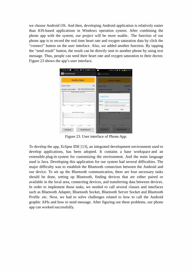
we choose Android OS. And then, developing Android application is relatively easier
than IOS-based applications in Windows operation system. After combining the
phone app with the system, our project will be more usable.. The function of our
phone app is to record the real time heart rate and oxygen saturation data by click the
“connect” button on the user interface. Also, we added another function. By tapping
the “send result” button, the result can be directly sent to another phone by using text
message. Thus, people can send their heart rate and oxygen saturation to their doctor.
Figure 23 shows the app’s user interface.
Figure 23. User interface of Phone App.
To develop the app, Eclipse IDE [13], an integrated development environment used to
develop applications, has been adopted. It contains a base workspace and an
extensible plug-in system for customizing the environment. And the main language
used is Java. Developing this application for our system had several difficulties. The
major difficulty was to establish the Bluetooth connection between the Android and
our device. To set up the Bluetooth communication, there are four necessary tasks
should be done, setting up Bluetooth, finding devices that are either paired or
available in the local area, connecting devices, and transferring data between devices.
In order to implement those tasks, we needed to call several classes and interfaces
such as Bluetooth Adapter, Bluetooth Socket, Bluetooth Server Socket and Bluetooth
Profile .etc. Next, we had to solve challenges related to how to call the Android
graphic APIs and how to send message. After figuring out these problems, our phone
app can worked successfully.
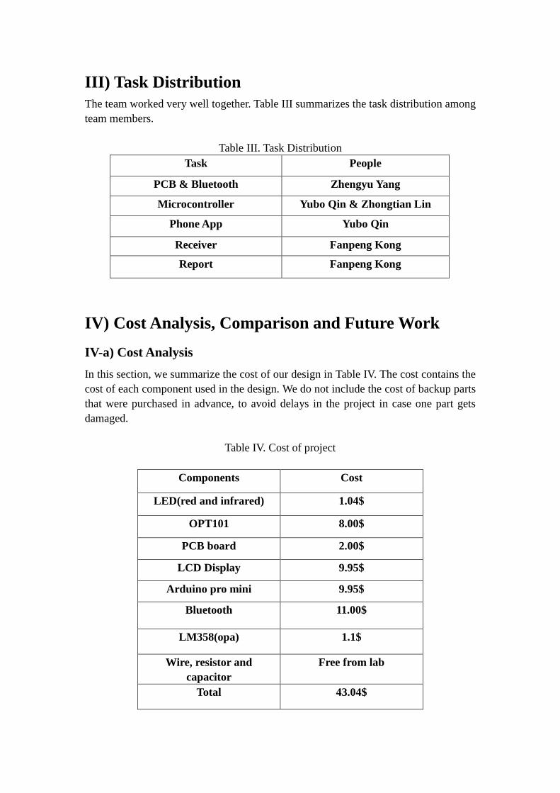
III) Task Distribution
The team worked very well together. Table III summarizes the task distribution among
team members.
Table III. Task Distribution
Task People
PCB & Bluetooth Zhengyu Yang
Microcontroller Yubo Qin & Zhongtian Lin
Phone App Yubo Qin
Receiver Fanpeng Kong
Report Fanpeng Kong
IV) Cost Analysis, Comparison and Future Work
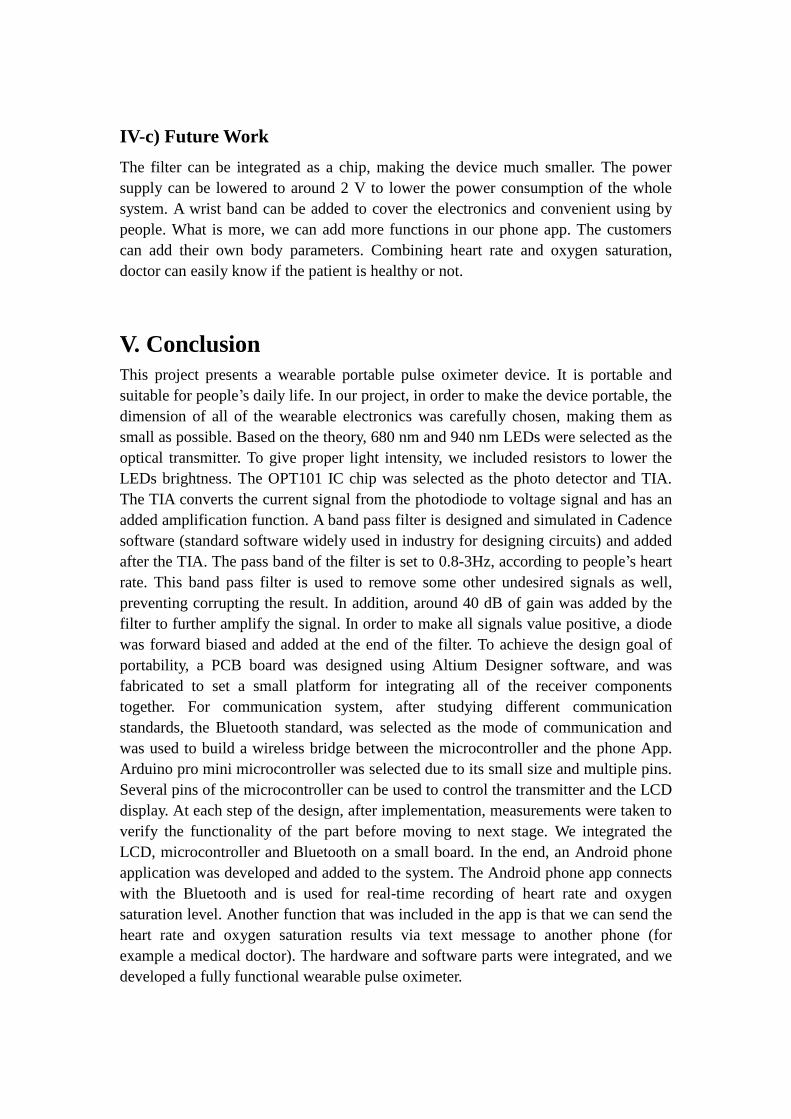
IV-a) Cost Analysis
In this section, we summarize the cost of our design in Table IV. The cost contains the
cost of each component used in the design. We do not include the cost of backup parts
that were purchased in advance, to avoid delays in the project in case one part gets
damaged.
Table IV. Cost of project
Components Cost
LED(red and infrared) 1.04$
OPT101 8.00$
PCB board 2.00$
LCD Display 9.95$
Arduino pro mini 9.95$
Bluetooth 11.00$
LM358(opa) 1.1$
Wire, resistor and
capacitor
Free from lab
Total 43.04$

Figure 24 shows the picture of the final product.
Figure 24. Final pulse oximeter system
IV-b) Comparison
Today, there exists different types of pulse oximeters in the market. Table V compares
the cost and performance of few commercial products with the system from our
capstone project. The comparison is focused on the cost, phone application
availability, pulse rate and oxygen saturation range, and dimension.
Compared to what exists in the market, our device offers less cost while having
comparable accuracy and offering the phone app with the applicability of texting the
heart-rate information in real-time to medical doctor.
Table V. Comparison
Device
Pulse Rate
Resolution
SpO2
Accuracy
Phone
App
Dimension
(mm)
Cost
($)
Pulse Oximeter
CMS50DL [14]
+-1bpm
+-1%
No
57*31*34
35
Wrist Pulse
Oximeter
PC-68A [15]
+-1bpm
+-1%
No
59*49*22
239.99
Santamedical
SM-240 [16]
+-1bpm
+-1%
No
NA
199
This Work
+-0.1bpm
+-0.1%
Yes
41*31*35
43
IV-c) Future Work
The filter can be integrated as a chip, making the device much smaller. The power
supply can be lowered to around 2 V to lower the power consumption of the whole
system. A wrist band can be added to cover the electronics and convenient using by
people. What is more, we can add more functions in our phone app. The customers
can add their own body parameters. Combining heart rate and oxygen saturation,
doctor can easily know if the patient is healthy or not.
V. Conclusion
This project presents a wearable portable pulse oximeter device. It is portable and
suitable for people’s daily life. In our project, in order to make the device portable, the
dimension of all of the wearable electronics was carefully chosen, making them as
small as possible. Based on the theory, 680 nm and 940 nm LEDs were selected as the
optical transmitter. To give proper light intensity, we included resistors to lower the
LEDs brightness. The OPT101 IC chip was selected as the photo detector and TIA.
The TIA converts the current signal from the photodiode to voltage signal and has an
added amplification function. A band pass filter is designed and simulated in Cadence
software (standard software widely used in industry for designing circuits) and added
after the TIA. The pass band of the filter is set to 0.8-3Hz, according to people’s heart
rate. This band pass filter is used to remove some other undesired signals as well,
preventing corrupting the result. In addition, around 40 dB of gain was added by the
filter to further amplify the signal. In order to make all signals value positive, a diode
was forward biased and added at the end of the filter. To achieve the design goal of
portability, a PCB board was designed using Altium Designer software, and was
fabricated to set a small platform for integrating all of the receiver components
together. For communication system, after studying different communication
standards, the Bluetooth standard, was selected as the mode of communication and
was used to build a wireless bridge between the microcontroller and the phone App.
Arduino pro mini microcontroller was selected due to its small size and multiple pins.
Several pins of the microcontroller can be used to control the transmitter and the LCD
display. At each step of the design, after implementation, measurements were taken to
verify the functionality of the part before moving to next stage. We integrated the
LCD, microcontroller and Bluetooth on a small board. In the end, an Android phone
application was developed and added to the system. The Android phone app connects
with the Bluetooth and is used for real-time recording of heart rate and oxygen
saturation level. Another function that was included in the app is that we can send the
heart rate and oxygen saturation results via text message to another phone (for
example a medical doctor). The hardware and software parts were integrated, and we
developed a fully functional wearable pulse oximeter.

References
[1] Young-Dong Lee, Sang-Joong Jung, Yong-Su Seo and Wan-Young Chung “Measurement
of Motion Activity during Ambulatory Using Pulse Oximeter and Triaxial Accelerometer” Third
2008 International Conference on Convergence and Hybrid Information Technology
[2] OPT101 Datasheet Texas Instrument. http://www.ti.com/lit/ds/symlink/opt101.pdf
[3] http://www.cadence.com/us/pages/default.aspx
[4] http://www.altium.com/en/products/altium-designer
[5] http://www.merl.rutgers.edu
[6] http://www.bluetooth.com/Pages/Bluetooth-Home.aspx
[7] http://www.tutorialspoint.com/wi-fi/wifi_ieee_standards.htm
[8] http://www.nearfieldcommunication.org/technology.html
[9] Mgchemical Product Catalog.
http://www.mgchemicals.com/downloads/catalog/index.html#page/1
[10] http://www.adafruit.com/products/1222
[11] http://arduino.cc/en/Main/ArduinoBoardProMini
[12] http://arduino.cc/en/main/software
[13] https://www.eclipse.org/downloads/
[14] http://www.clinicalguard.com/fingertip-pulse-oximeter-cms50dl-p-161.html
[15] http://www.favoriteplus.com/wrist-pulse-oximeter-pc-68b.php
[16] http://santamedical.com/santamedicalsm-240oledfingerpulseoximeter.aspx
Appendix
Ardunio Code
#include <LiquidCrystal.h> //LCD #include"floatToString.h"
#include <SoftwareSerial.h> //bluetooth
#include <TimerOne.h> //interrupts
#define analogPin A0
#define Theta 0.6
#define RxD 1 //bluetooth read
#define TxD 0 //bluetooth transmit
#define DEBUG_ENABLED //bluetooth
#define redLED 11 //High is Red led on, Low is Infrared on.
//#define iredLED 12
volatile int maxTemp,minTemp; //shared variables between interrupts and loop
volatile int lastcount,count;
int Rmax, Rmin, IRmax, IRmin;
float R, Spo2,HeartR_frq;
int Sp02_int;

int HeartRate, HeartR;
float LastHeartRate = 70; //default
int average = 140; //average is average crossing
//int average2 = 220;
int interrupts_counter =0; //count the times of interrupts
float value=0.5;
float Spo2_float;
char buffer[25];
SoftwareSerial blueToothSerial(RxD,TxD); //define bluetooth
void setup()
{
pinMode(redLED, OUTPUT); //define LED
pinMode(RxD, INPUT); //bluetooth input
pinMode(TxD, OUTPUT); //bluetooth output
pinMode(analogPin, INPUT); //analog signal input
//initially switch on Red LED, after each interrupt will turn on the other
digitalWrite(redLED, HIGH);
Serial.begin(9600);
//bluetooth
setupBlueToothConnection();
//initialize LCD
LiquidCrystal lcd(8, 9, 4, 5, 6, 7); // initialize LCD, the pins are all depends
lcd.begin(8, 2); //set up the LCD's number of columns and rows:
lcd.clear();
init_interrupts();
Timer1.initialize(40000); //terrupt every 0.04 seconds
Timer1.attachInterrupt(max_min_num); //interrupt call max_min_num function
Rmax = 0;
IRmax = 0;
Rmin = 0;
IRmin = 0;
LastHeartRate = 70;
}
void setupBlueToothConnection() //initialize bluetooth
{
blueToothSerial.begin(9600); //Set BluetoothBee BaudRate to default baud rate
38400
blueToothSerial.print("\r\n+STWMOD=0\r\n"); //t the bluetooth work in slave
mode
blueToothSerial.print("\r\n+STNA=HC-06\r\n"); //t the bluetooth name as "HC-05"
blueToothSerial.print("\r\n+STOAUT=1\r\n"); // Permit Paired device to connect

me
blueToothSerial.print("\r\n+STAUTO=0\r\n"); // Auto-connection should be
forbidden here
delay(2000); // This delay is required.
//blueToothSerial.print("\r\n+INQ=1\r\n"); //make the slave bluetooth inquirable
blueToothSerial.print("bluetooth connected!\n");
delay(2000); // This delay is required.
blueToothSerial.flush();
}
void max_min_num()
{
lastcount = count;
count = analogRead(analogPin); //read signa
if(count> maxTemp){
maxTemp = count;
}
else if(count<minTemp){
minTemp = count;
}
interrupts_counter++; //interrupt counter
}
void init_interrupts()
{
maxTemp = 0;
minTemp = 1023;
count = 0;
lastcount =0;
interrupts_counter = 0;
}
void loop(){
//initialize LCD
LiquidCrystal lcd(8, 9, 4, 5, 6, 7); // initialize LCD, the pins are all depends
lcd.begin(8, 2); //set up the LCD's number of columns and rows:
while(1){ //the whole while is used to avoid LCD reinitialize
digitalWrite(redLED,HIGH);
delay(2000); //let red led signal to be stable
//interrupts();
while(!((lastcount>average )&& (count<average)) ){ }
digitalWrite(redLED,HIGH);
init_interrupts();
while(!((lastcount>average )&& (count<average)) ){ }

noInterrupts(); // temporarily disabel interrupts, to be sure it will not change while
we are reading
Rmax = maxTemp;
Rmin = minTemp;
delay(100);
HeartR_frq = 1/(0.04*interrupts_counter); //d is the times of ISR in 1 second,
interrupts(); //enable interrupts
HeartRate = HeartR_frq * 60;
if(HeartRate> 60 && HeartRate< 120){
HeartR = Theta*HeartRate + (1 - Theta)*LastHeartRate; //Use theta to smooth
LastHeartRate = HeartR;
}
digitalWrite(redLED, LOW);
//initialize lcd
lcd.setCursor(0,0);
lcd.print("HR:");
lcd.setCursor(5,0);
lcd.print(HeartR);
R = (Rmax - Rmin);
Spo2 = (R-180)*0.01 +97.838;
int Spo2_int = (int)Spo2; //float Spo2 to int Spo2_int
String Spo2_float = floatToString(buffer,Spo2,2);
lcd.setCursor(0,1);
lcd.print("SPO2:");
lcd.setCursor(5,1);
lcd.print(Spo2_int);
//transmit data to phone app through bluetooth
String H = String("H")+HeartR +String("S") +Spo2_float;
Serial.println(H);
delay(1000);
init_interrupts();
}
}