Embed Size (px)
Citation preview
Chapter 11Thyristors And Other
Devices
Objectives Describe the basic structure and operation of the Shockley diode
Describe the basic structure and operation of a silicon controlled rectifier and applications of an SCR Describe the basic operation of the SCS
Describe the basic operation of diacs and triacs
Objectives Describe the basic operation of UJTs and PUTs
Describe the basic operation of a phototransistor Describe the basic operation of a Light Activated SCR Describe the various types of optical couplers
Describe the basic operation of the insulated-gate bipolar transistor.
Discuss fiber optic basics
Describe the various types of optical couplers
Introduction
The devices covered in this chapter are mainly used in industrial applications where power control and switching are needed.
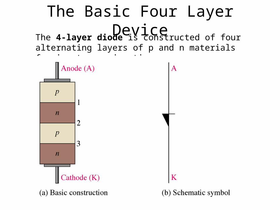
The Basic Four Layer DeviceThe 4-layer diode is constructed of four alternating layers of p and n materials forming two pn junctions.
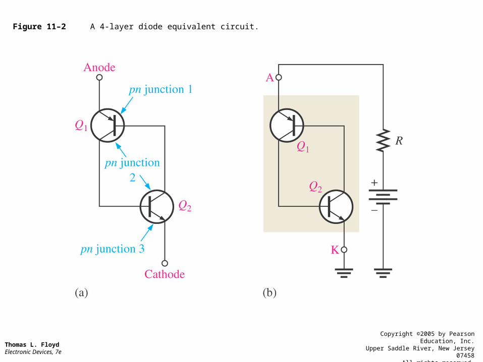
Figure 11–2 A 4-layer diode equivalent circuit.
Thomas L. Floyd Electronic Devices, 7e
Copyright ©2005 by Pearson Education, Inc.Upper Saddle River, New Jersey 07458
All rights reserved.
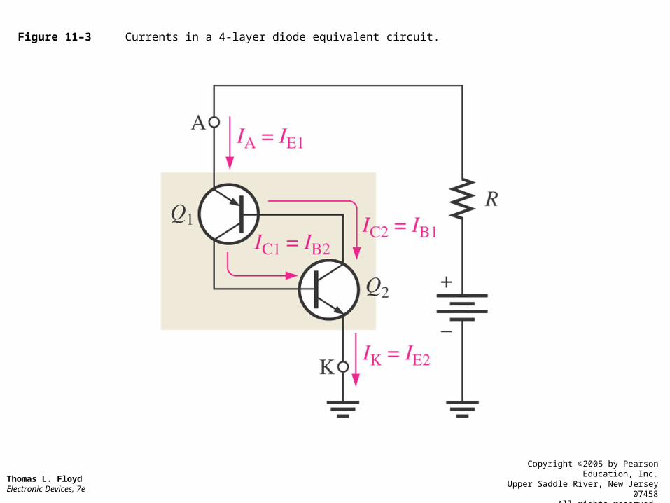
Figure 11–3 Currents in a 4-layer diode equivalent circuit.
Thomas L. Floyd Electronic Devices, 7e
Copyright ©2005 by Pearson Education, Inc.Upper Saddle River, New Jersey 07458
All rights reserved.
The Basic Four Layer Device
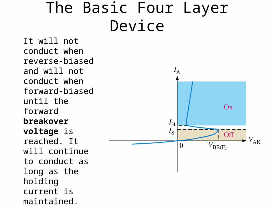
It will not conduct when reverse-biased and will not conduct when forward-biased until the forward breakover voltage is reached. It will continue to conduct as long as the holding current is maintained. The region prior to breakover is called the forward blocking region.
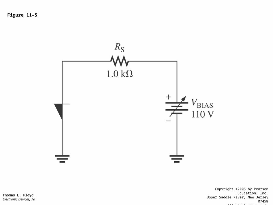
Figure 11–5
Thomas L. Floyd Electronic Devices, 7e
Copyright ©2005 by Pearson Education, Inc.Upper Saddle River, New Jersey 07458
All rights reserved.
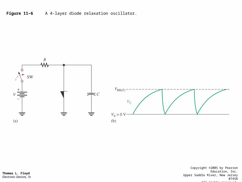
Figure 11–6 A 4-layer diode relaxation oscillator.
Thomas L. Floyd Electronic Devices, 7e
Copyright ©2005 by Pearson Education, Inc.Upper Saddle River, New Jersey 07458
All rights reserved.
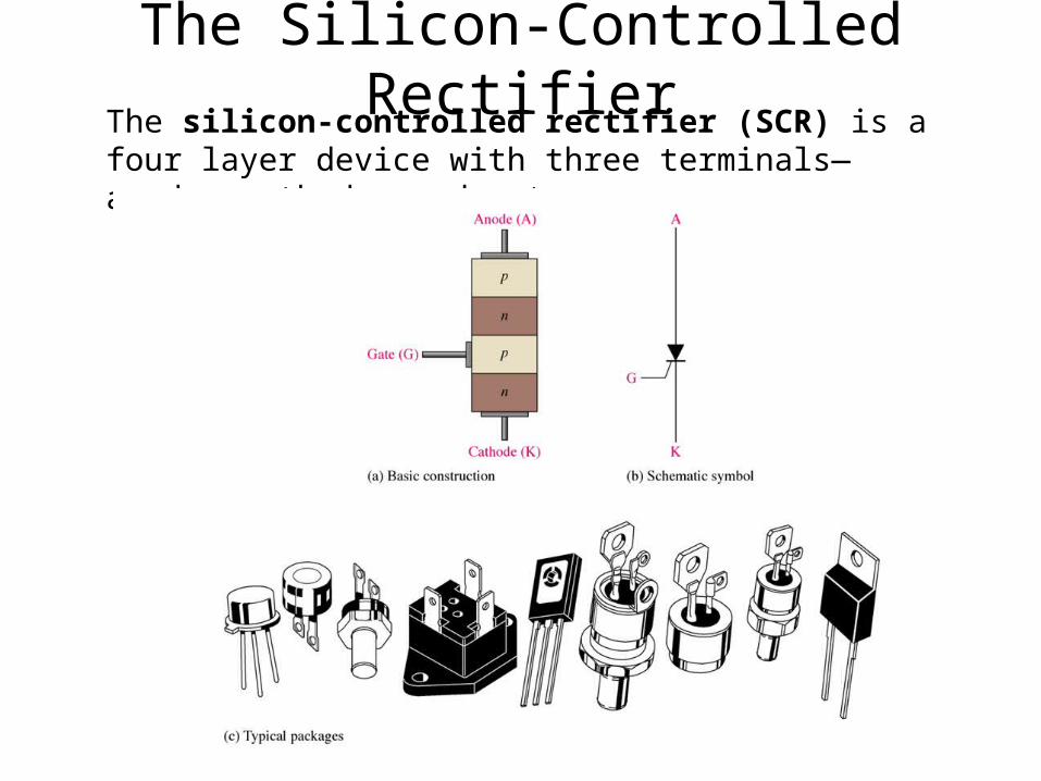
The Silicon-Controlled RectifierThe silicon-controlled rectifier (SCR) is a four layer device with three terminals— anode, cathode, and gate.
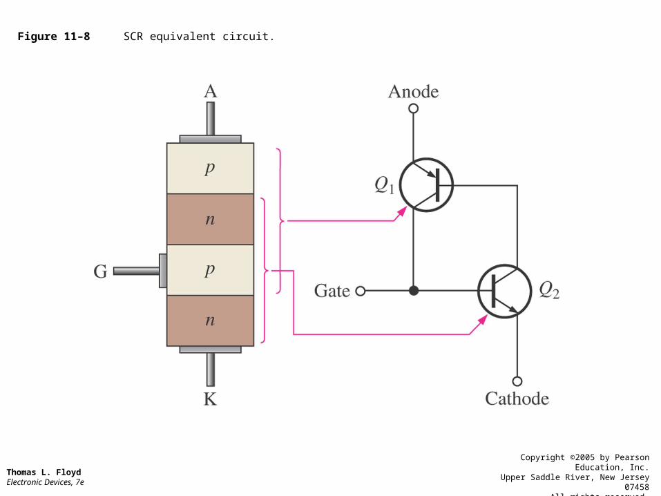
Figure 11–8 SCR equivalent circuit.
Thomas L. Floyd Electronic Devices, 7e
Copyright ©2005 by Pearson Education, Inc.Upper Saddle River, New Jersey 07458
All rights reserved.
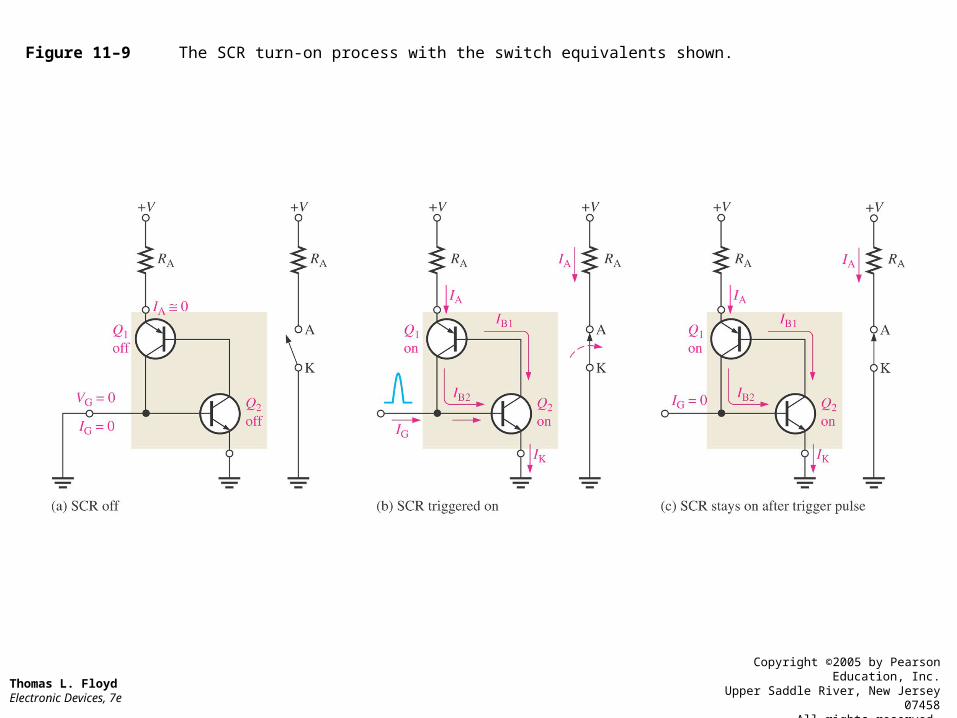
Figure 11–9 The SCR turn-on process with the switch equivalents shown.
Thomas L. Floyd Electronic Devices, 7e
Copyright ©2005 by Pearson Education, Inc.Upper Saddle River, New Jersey 07458
All rights reserved.
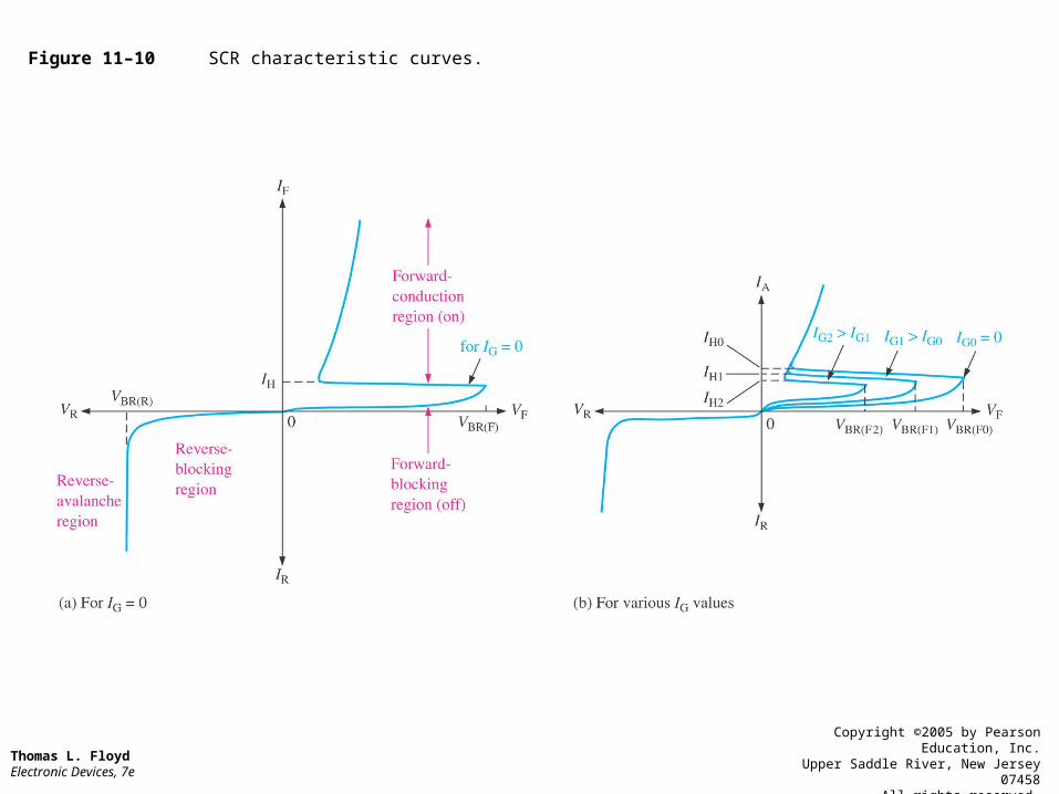
Figure 11–10 SCR characteristic curves.
Thomas L. Floyd Electronic Devices, 7e
Copyright ©2005 by Pearson Education, Inc.Upper Saddle River, New Jersey 07458
All rights reserved.
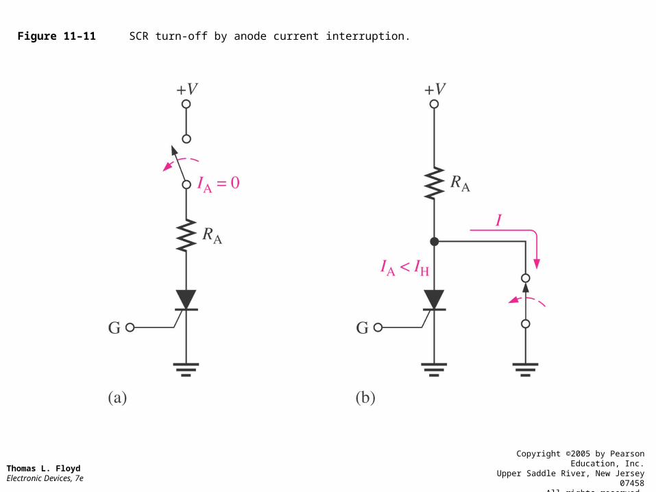
Figure 11–11 SCR turn-off by anode current interruption.
Thomas L. Floyd Electronic Devices, 7e
Copyright ©2005 by Pearson Education, Inc.Upper Saddle River, New Jersey 07458
All rights reserved.
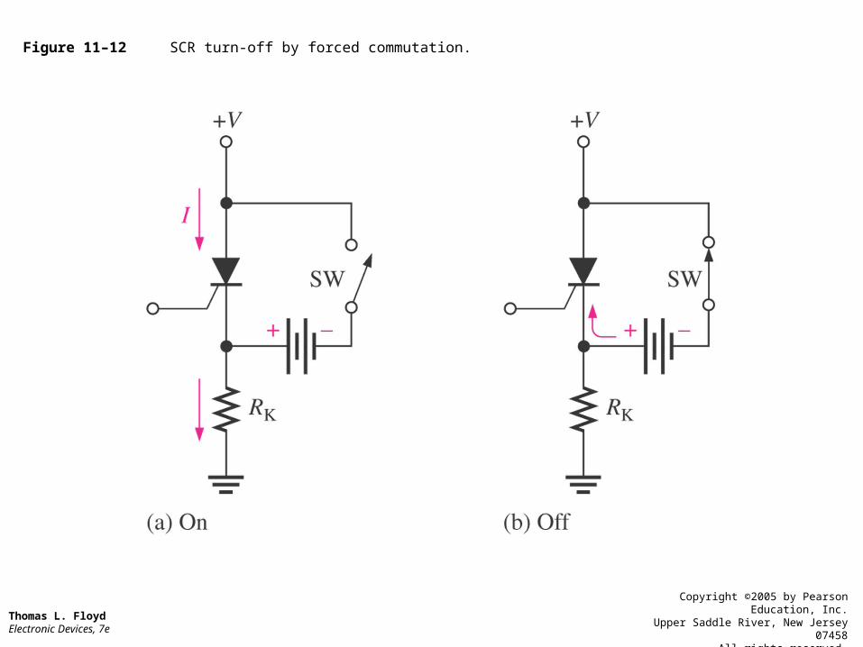
Figure 11–12 SCR turn-off by forced commutation.
Thomas L. Floyd Electronic Devices, 7e
Copyright ©2005 by Pearson Education, Inc.Upper Saddle River, New Jersey 07458
All rights reserved.
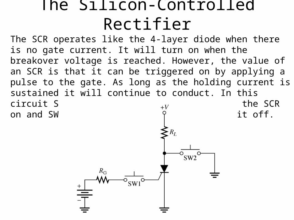
The Silicon-Controlled RectifierThe SCR operates like the 4-layer diode when there is no gate current. It will turn on when the breakover voltage is reached. However, the value of an SCR is that it can be triggered on by applying a pulse to the gate. As long as the holding current is sustained it will continue to conduct. In this circuit SW1 is pressed momentarily to turn the SCR on and SW2 is pressed momentarily to turn it off.
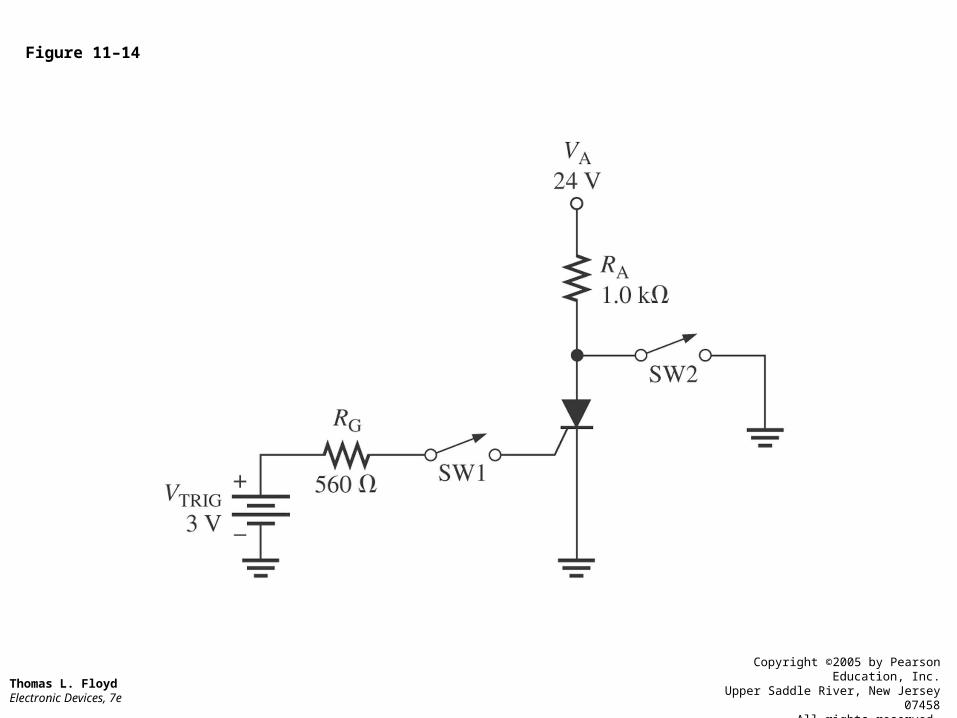
Figure 11–14
Thomas L. Floyd Electronic Devices, 7e
Copyright ©2005 by Pearson Education, Inc.Upper Saddle River, New Jersey 07458
All rights reserved.
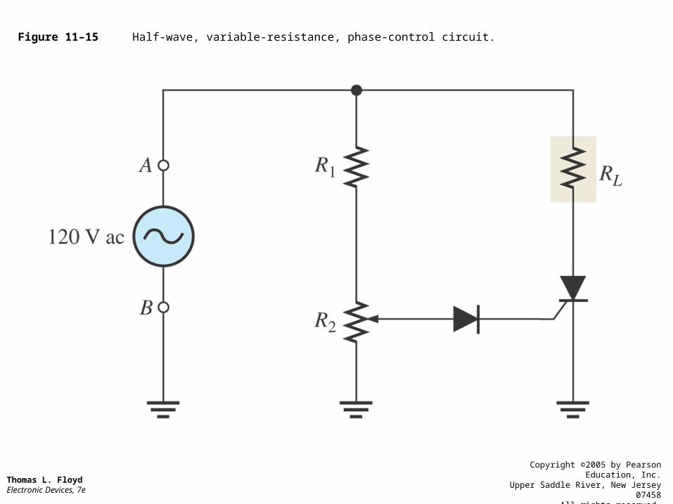
Figure 11–15 Half-wave, variable-resistance, phase-control circuit.
Thomas L. Floyd Electronic Devices, 7e
Copyright ©2005 by Pearson Education, Inc.Upper Saddle River, New Jersey 07458
All rights reserved.
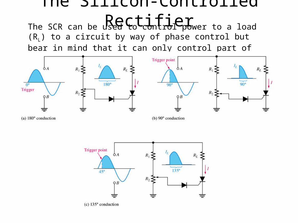
The Silicon-Controlled RectifierThe SCR can be used to control power to a load (RL) to a circuit by way of phase control but bear in mind that it can only control part of half the signal since it will not conduct in reverse bias.
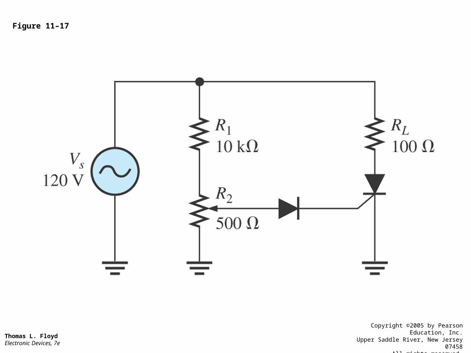
Figure 11–17
Thomas L. Floyd Electronic Devices, 7e
Copyright ©2005 by Pearson Education, Inc.Upper Saddle River, New Jersey 07458
All rights reserved.
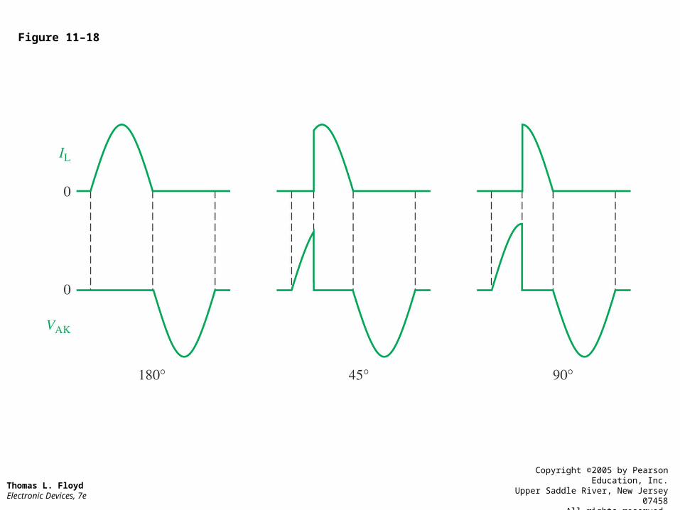
Figure 11–18
Thomas L. Floyd Electronic Devices, 7e
Copyright ©2005 by Pearson Education, Inc.Upper Saddle River, New Jersey 07458
All rights reserved.
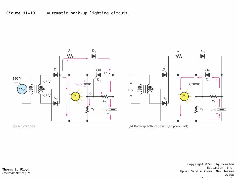
Figure 11–19 Automatic back-up lighting circuit.
Thomas L. Floyd Electronic Devices, 7e
Copyright ©2005 by Pearson Education, Inc.Upper Saddle River, New Jersey 07458
All rights reserved.
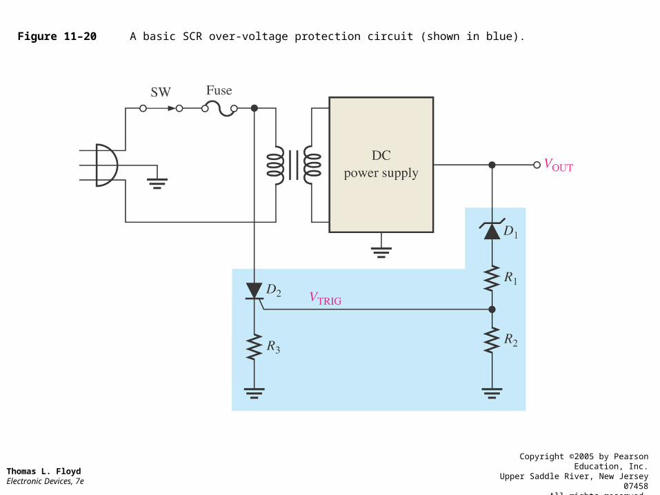
Figure 11–20 A basic SCR over-voltage protection circuit (shown in blue).
Thomas L. Floyd Electronic Devices, 7e
Copyright ©2005 by Pearson Education, Inc.Upper Saddle River, New Jersey 07458
All rights reserved.
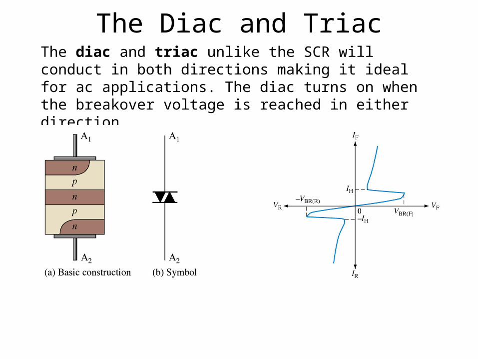
The Diac and TriacThe diac and triac unlike the SCR will conduct in both directions making it ideal for ac applications. The diac turns on when the breakover voltage is reached in either direction.
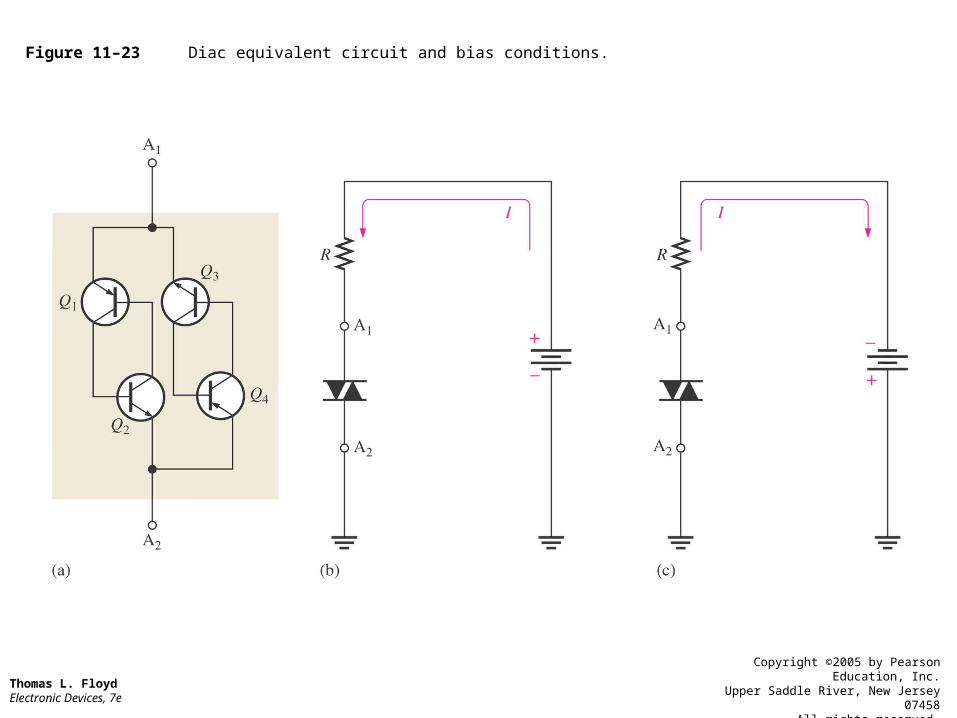
Figure 11–23 Diac equivalent circuit and bias conditions.
Thomas L. Floyd Electronic Devices, 7e
Copyright ©2005 by Pearson Education, Inc.Upper Saddle River, New Jersey 07458
All rights reserved.
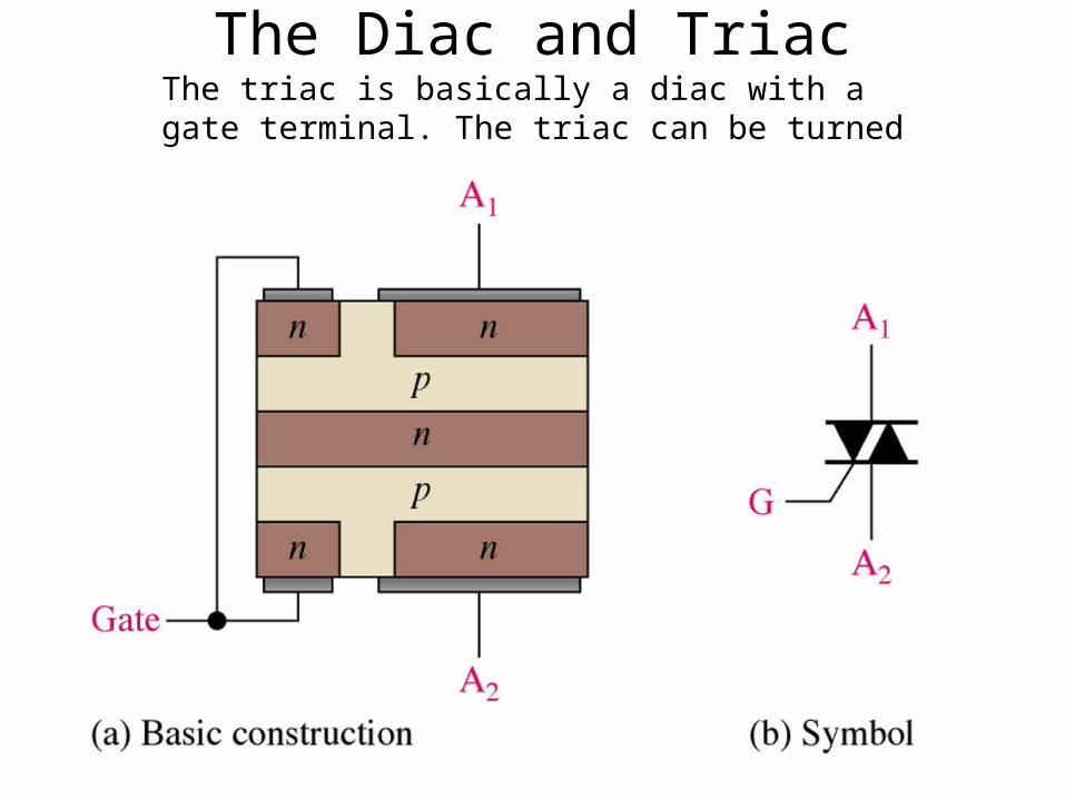
The Diac and TriacThe triac is basically a diac with a gate terminal. The triac can be turned by a pulse at the gate.
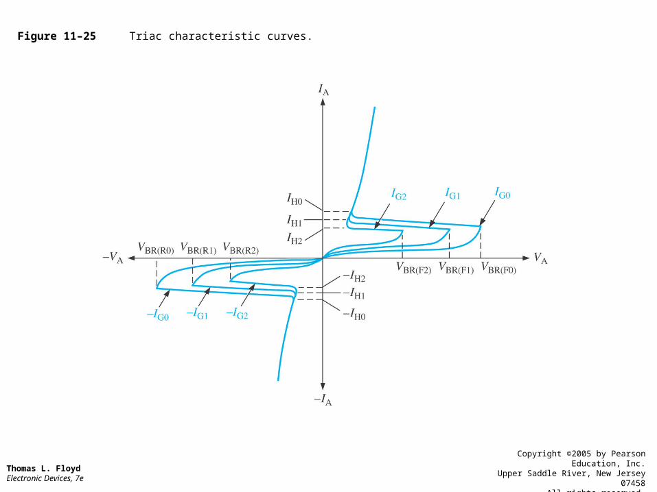
Figure 11–25 Triac characteristic curves.
Thomas L. Floyd Electronic Devices, 7e
Copyright ©2005 by Pearson Education, Inc.Upper Saddle River, New Jersey 07458
All rights reserved.
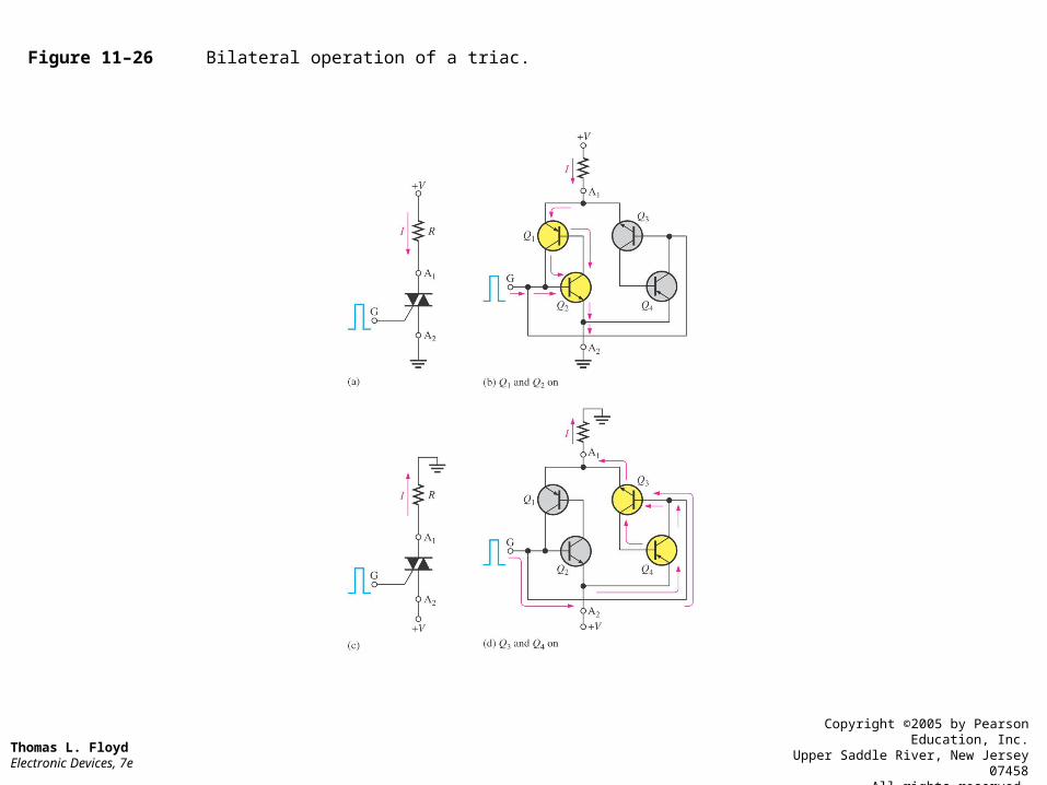
Figure 11–26 Bilateral operation of a triac.
Thomas L. Floyd Electronic Devices, 7e
Copyright ©2005 by Pearson Education, Inc.Upper Saddle River, New Jersey 07458
All rights reserved.
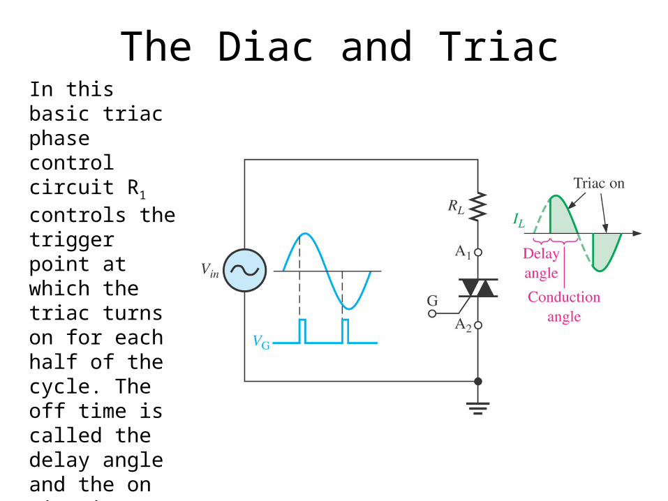
The Diac and TriacIn this basic triac phase control circuit R1 controls the trigger point at which the triac turns on for each half of the cycle. The off time is called the delay angle and the on time is called the conduction angle.
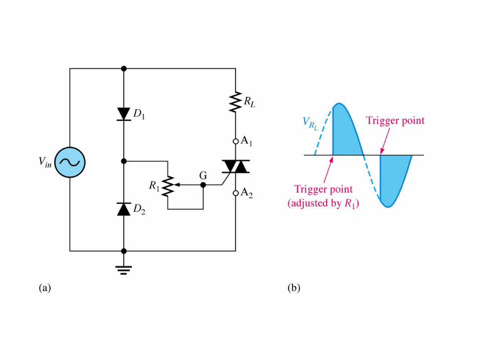
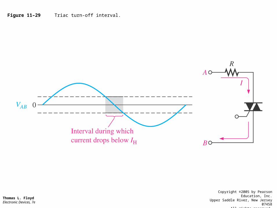
Figure 11–29 Triac turn-off interval.
Thomas L. Floyd Electronic Devices, 7e
Copyright ©2005 by Pearson Education, Inc.Upper Saddle River, New Jersey 07458
All rights reserved.
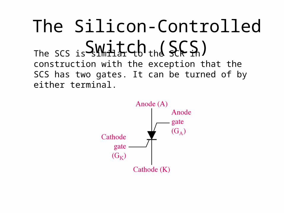
The Silicon-Controlled Switch (SCS)The SCS is similar to the SCR in construction with
the exception that the SCS has two gates. It can be turned of by either terminal.
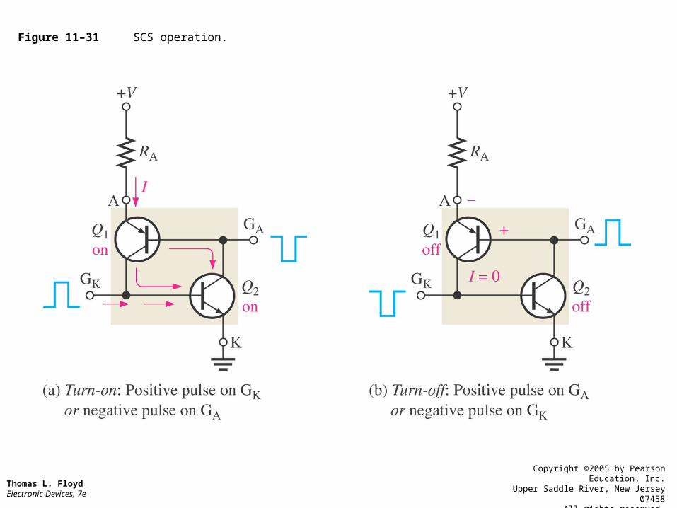
Figure 11–31 SCS operation.
Thomas L. Floyd Electronic Devices, 7e
Copyright ©2005 by Pearson Education, Inc.Upper Saddle River, New Jersey 07458
All rights reserved.
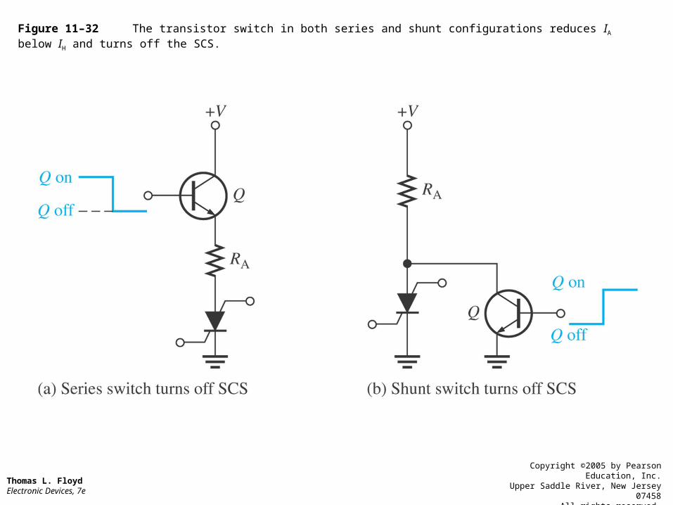
Figure 11–32 The transistor switch in both series and shunt configurations reduces IA below IH and turns off the SCS.
Thomas L. Floyd Electronic Devices, 7e
Copyright ©2005 by Pearson Education, Inc.Upper Saddle River, New Jersey 07458
All rights reserved.
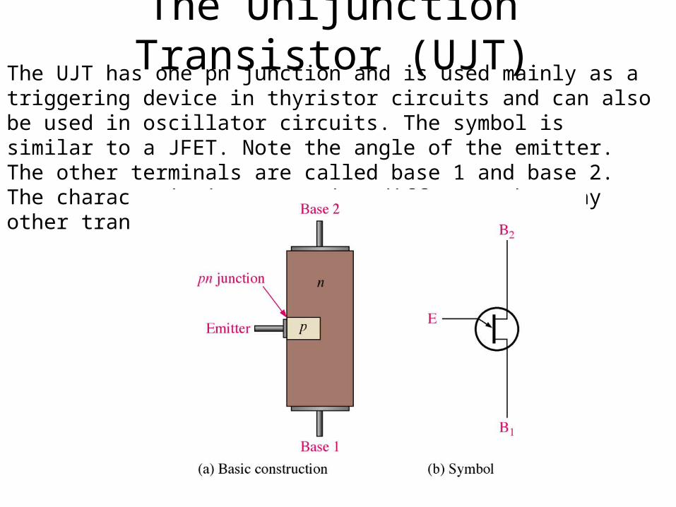
The Unijunction Transistor (UJT)The UJT has one pn junction and is used mainly as a triggering device in thyristor circuits and can also be used in oscillator circuits. The symbol is similar to a JFET. Note the angle of the emitter. The other terminals are called base 1 and base 2. The characteristics are quite different than any other transistor.
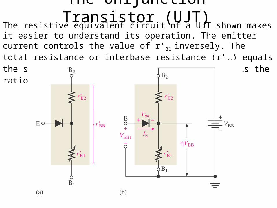
The Unijunction Transistor (UJT)The resistive equivalent circuit of a UJT shown makes it easier to understand its operation. The emitter current controls the value of r’B1 inversely. The total resistance or interbase resistance (r’BB) equals the sum of r’B1 and r’B2. The standoff ratio () is the ratio r’B1/ r’BB.
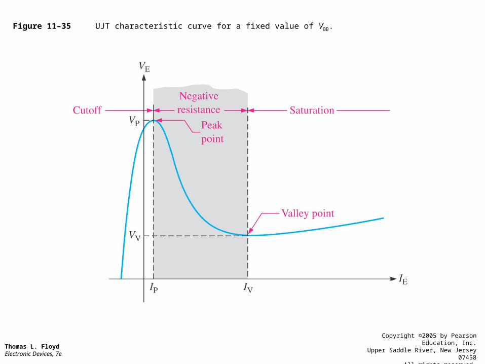
Figure 11–35 UJT characteristic curve for a fixed value of VBB.
Thomas L. Floyd Electronic Devices, 7e
Copyright ©2005 by Pearson Education, Inc.Upper Saddle River, New Jersey 07458
All rights reserved.
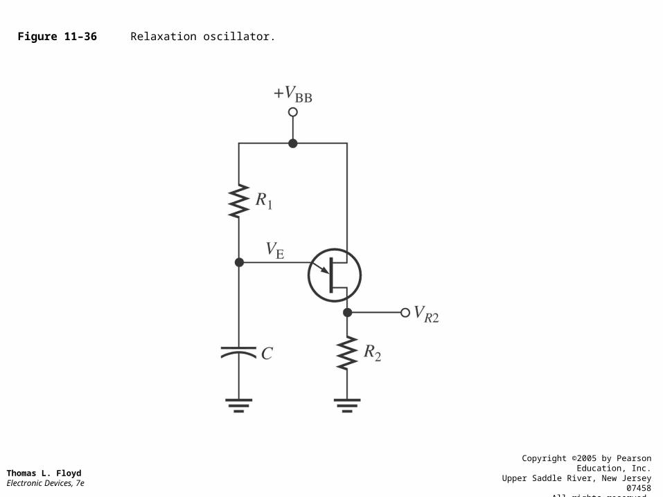
Figure 11–36 Relaxation oscillator.
Thomas L. Floyd Electronic Devices, 7e
Copyright ©2005 by Pearson Education, Inc.Upper Saddle River, New Jersey 07458
All rights reserved.
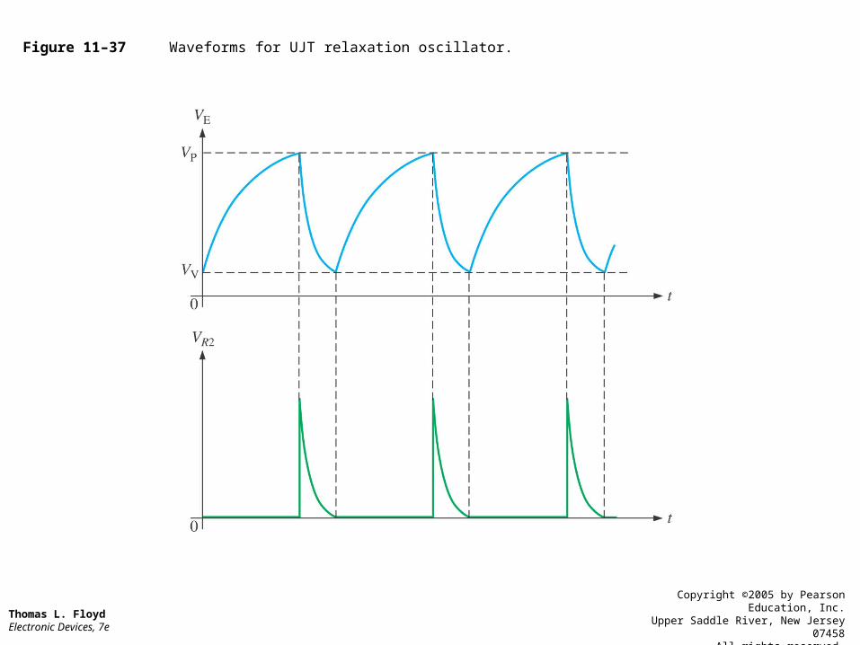
Figure 11–37 Waveforms for UJT relaxation oscillator.
Thomas L. Floyd Electronic Devices, 7e
Copyright ©2005 by Pearson Education, Inc.Upper Saddle River, New Jersey 07458
All rights reserved.
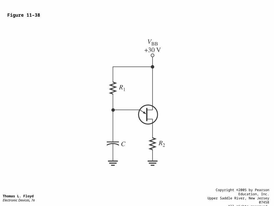
Figure 11–38
Thomas L. Floyd Electronic Devices, 7e
Copyright ©2005 by Pearson Education, Inc.Upper Saddle River, New Jersey 07458
All rights reserved.
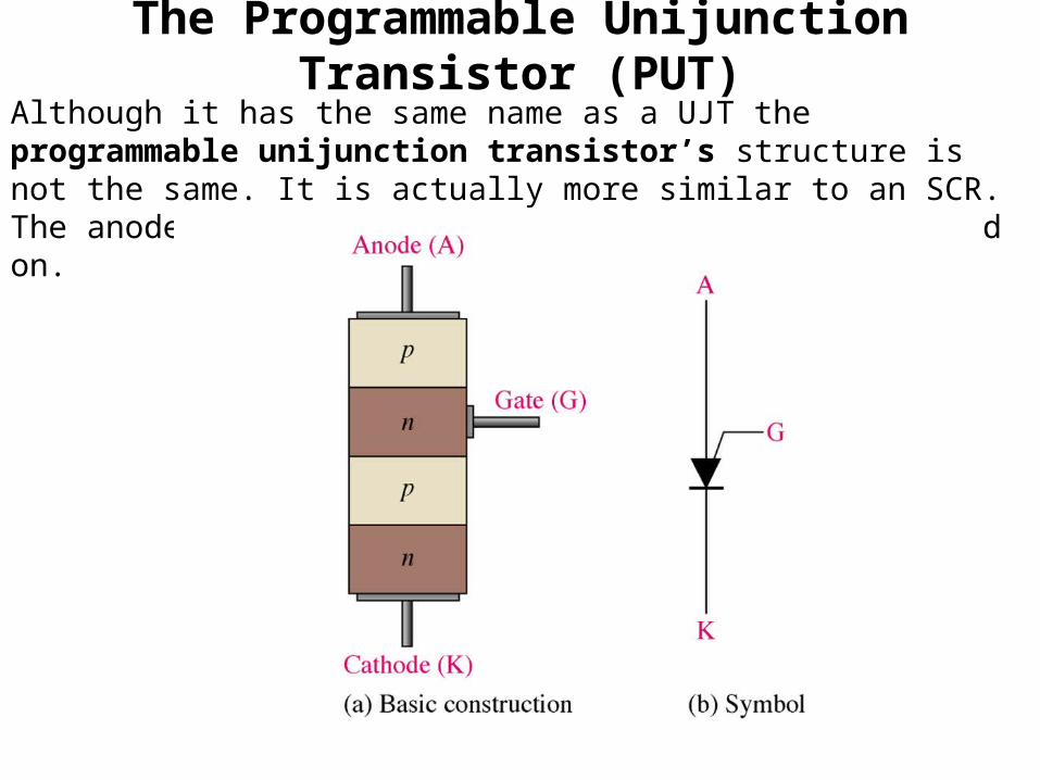
The Programmable Unijunction Transistor (PUT)Although it has the same name as a UJT the programmable unijunction transistor’s structure is not the same. It is actually more similar to an SCR. The anode to gate voltage is used to turn it off and on.
The Programmable Unijunction Transistor (PUT)
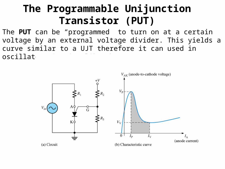
The PUT can be “programmed” to turn on at a certain voltage by an external voltage divider. This yields a curve similar to a UJT therefore it can used in oscillator circuits like the UJT.
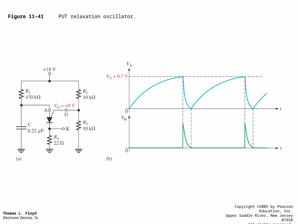
Figure 11–41 PUT relaxation oscillator.
Thomas L. Floyd Electronic Devices, 7e
Copyright ©2005 by Pearson Education, Inc.Upper Saddle River, New Jersey 07458
All rights reserved.
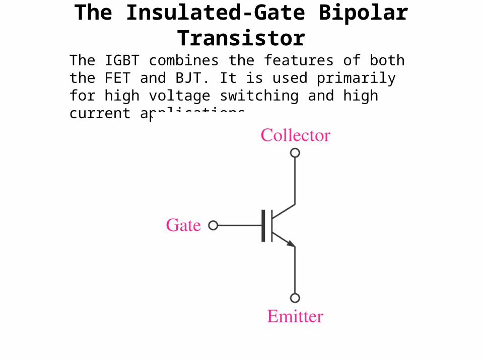
The Insulated-Gate Bipolar Transistor
The IGBT combines the features of both the FET and BJT. It is used primarily for high voltage switching and high current applications.
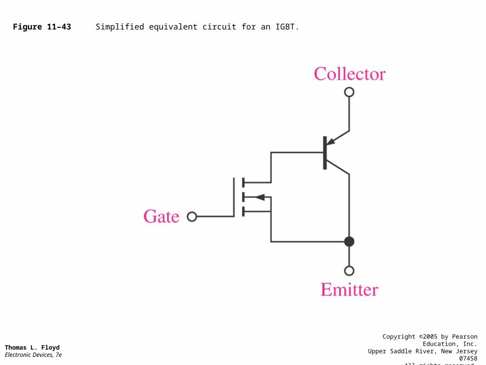
Figure 11–43 Simplified equivalent circuit for an IGBT.
Thomas L. Floyd Electronic Devices, 7e
Copyright ©2005 by Pearson Education, Inc.Upper Saddle River, New Jersey 07458
All rights reserved.
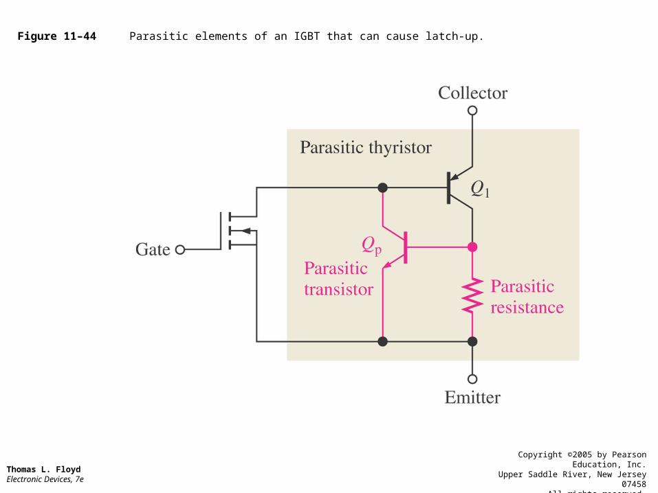
Figure 11–44 Parasitic elements of an IGBT that can cause latch-up.
Thomas L. Floyd Electronic Devices, 7e
Copyright ©2005 by Pearson Education, Inc.Upper Saddle River, New Jersey 07458
All rights reserved.
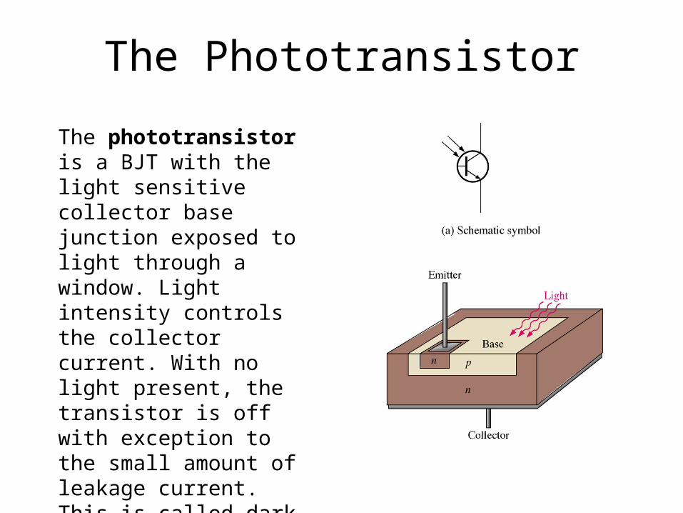
The Phototransistor
The phototransistor is a BJT with the light sensitive collector base junction exposed to light through a window. Light intensity controls the collector current. With no light present, the transistor is off with exception to the small amount of leakage current. This is called dark current.
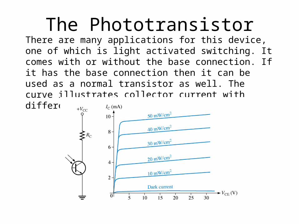
The PhototransistorThere are many applications for this device, one of which is light activated switching. It comes with or without the base connection. If it has the base connection then it can be used as a normal transistor as well. The curve illustrates collector current with different light intensities.
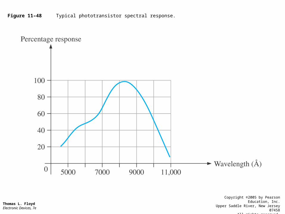
Figure 11–48 Typical phototransistor spectral response.
Thomas L. Floyd Electronic Devices, 7e
Copyright ©2005 by Pearson Education, Inc.Upper Saddle River, New Jersey 07458
All rights reserved.
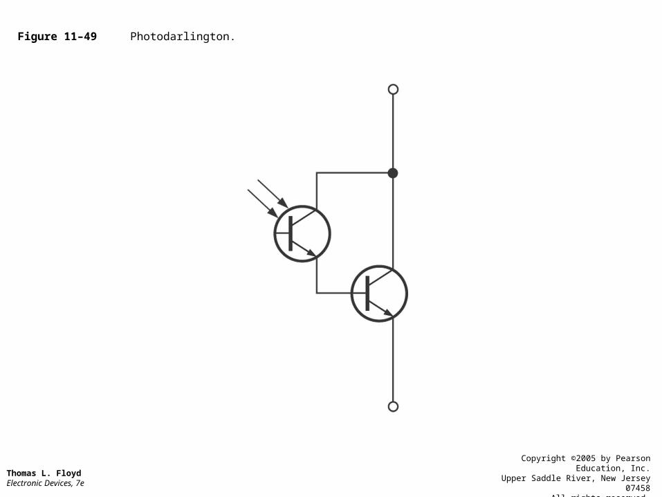
Figure 11–49 Photodarlington.
Thomas L. Floyd Electronic Devices, 7e
Copyright ©2005 by Pearson Education, Inc.Upper Saddle River, New Jersey 07458
All rights reserved.
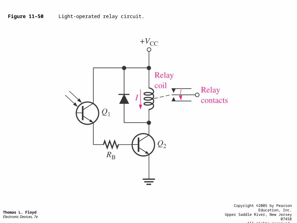
Figure 11–50 Light-operated relay circuit.
Thomas L. Floyd Electronic Devices, 7e
Copyright ©2005 by Pearson Education, Inc.Upper Saddle River, New Jersey 07458
All rights reserved.
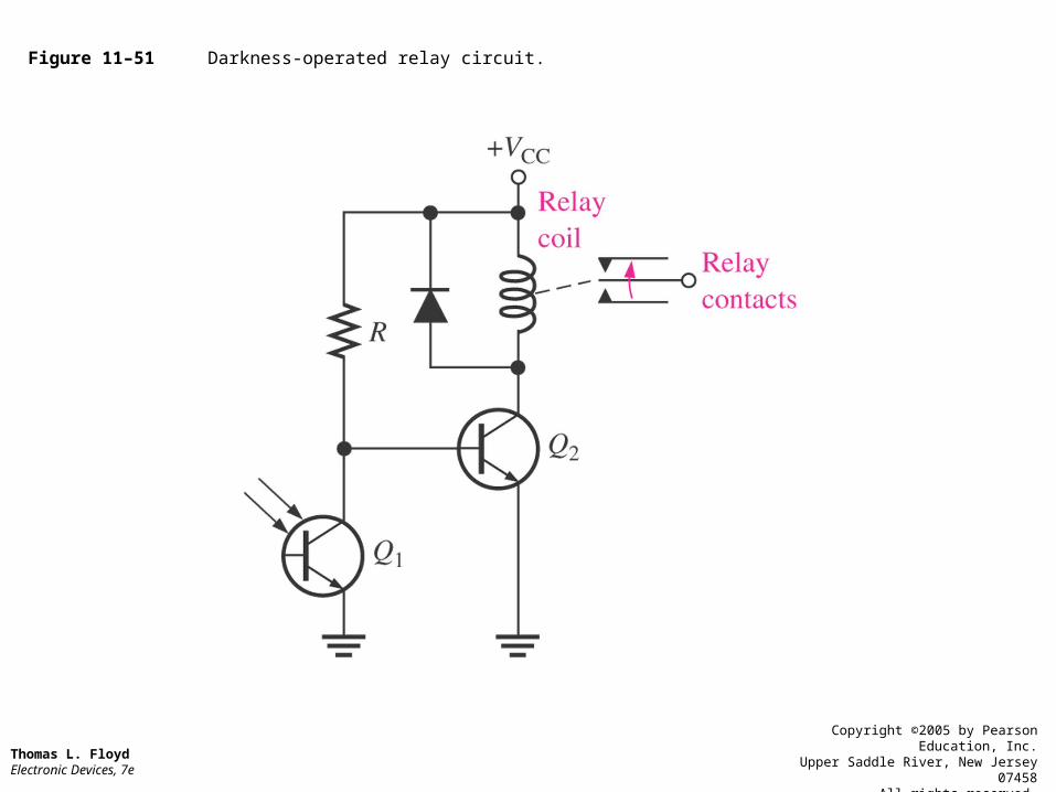
Figure 11–51 Darkness-operated relay circuit.
Thomas L. Floyd Electronic Devices, 7e
Copyright ©2005 by Pearson Education, Inc.Upper Saddle River, New Jersey 07458
All rights reserved.
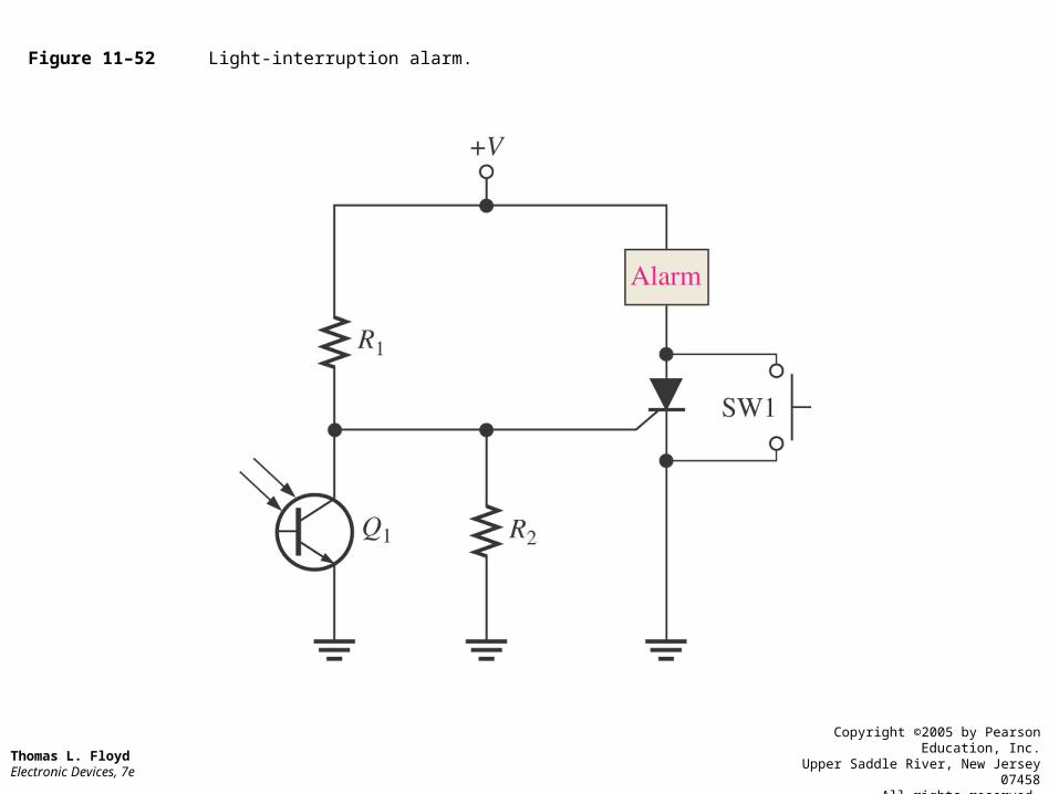
Figure 11–52 Light-interruption alarm.
Thomas L. Floyd Electronic Devices, 7e
Copyright ©2005 by Pearson Education, Inc.Upper Saddle River, New Jersey 07458
All rights reserved.
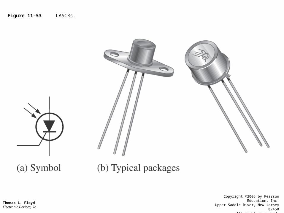
Figure 11–53 LASCRs.
Thomas L. Floyd Electronic Devices, 7e
Copyright ©2005 by Pearson Education, Inc.Upper Saddle River, New Jersey 07458
All rights reserved.
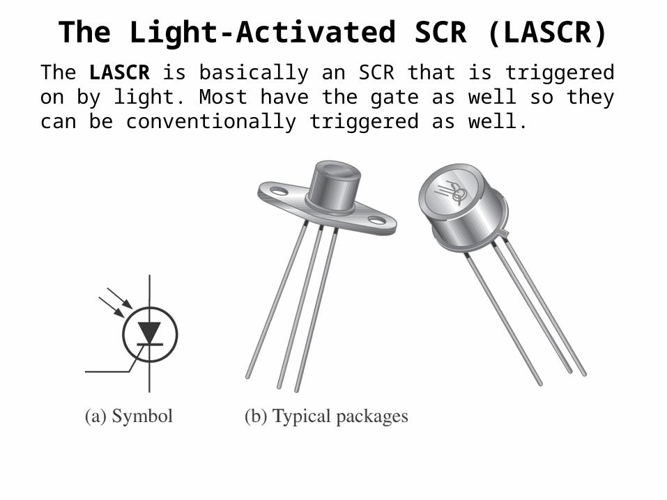
The Light-Activated SCR (LASCR)The LASCR is basically an SCR that is triggered on by light. Most have the gate as well so they can be conventionally triggered as well.
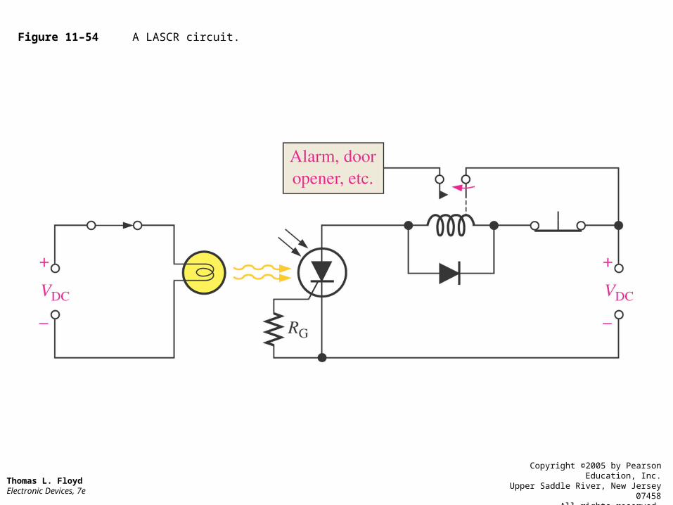
Figure 11–54 A LASCR circuit.
Thomas L. Floyd Electronic Devices, 7e
Copyright ©2005 by Pearson Education, Inc.Upper Saddle River, New Jersey 07458
All rights reserved.
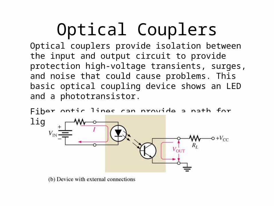
Optical CouplersOptical couplers provide isolation between the input and output circuit to provide protection high-voltage transients, surges, and noise that could cause problems. This basic optical coupling device shows an LED and a phototransistor.
Fiber optic lines can provide a path for light to travel between the devices.
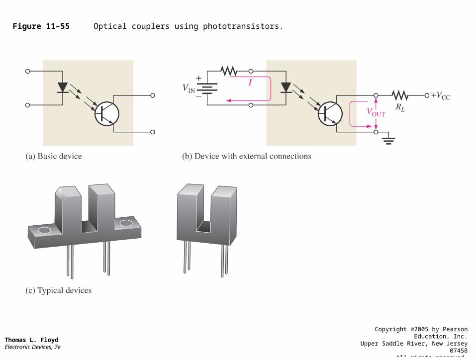
Figure 11–55 Optical couplers using phototransistors.
Thomas L. Floyd Electronic Devices, 7e
Copyright ©2005 by Pearson Education, Inc.Upper Saddle River, New Jersey 07458
All rights reserved.
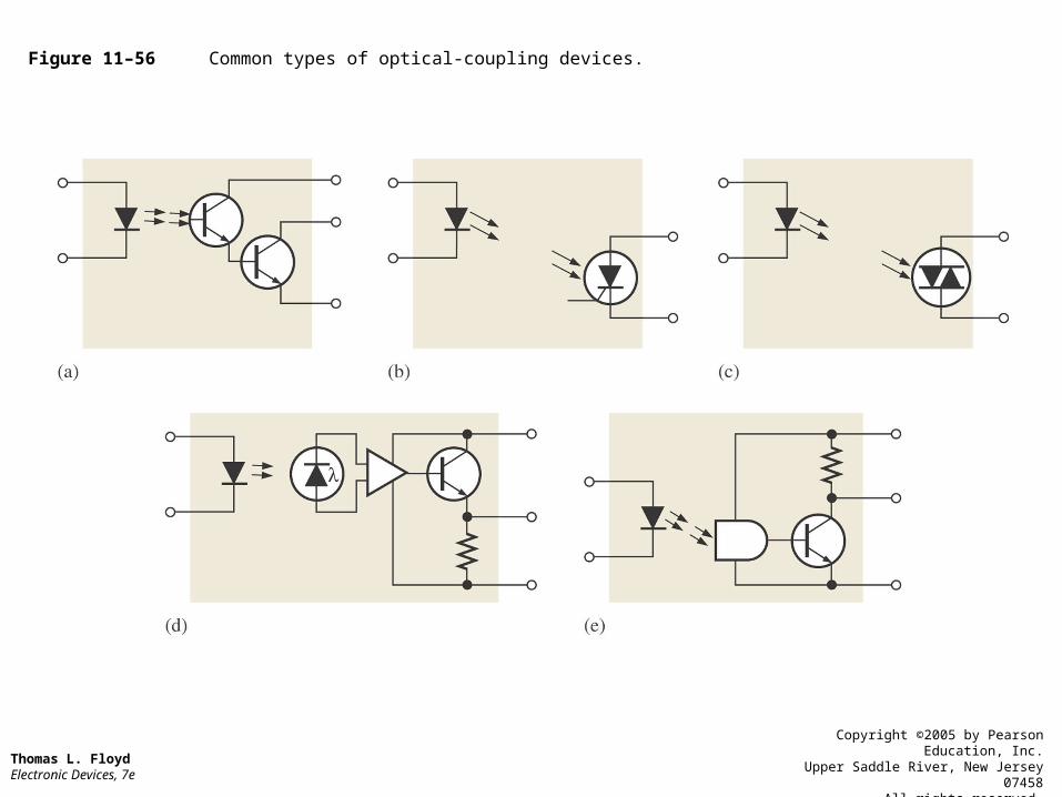
Figure 11–56 Common types of optical-coupling devices.
Thomas L. Floyd Electronic Devices, 7e
Copyright ©2005 by Pearson Education, Inc.Upper Saddle River, New Jersey 07458
All rights reserved.
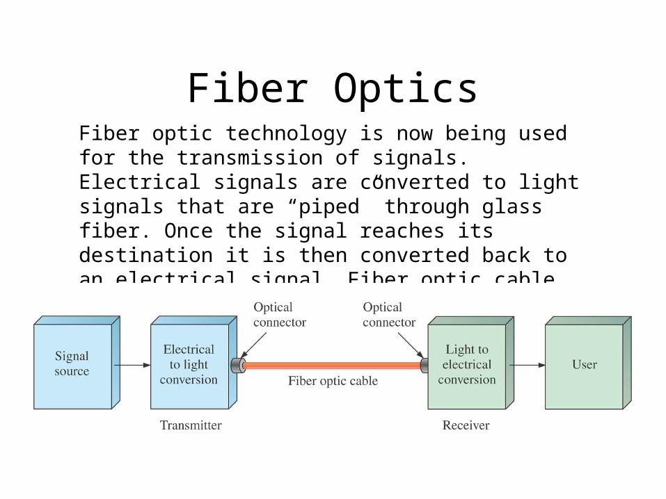
Fiber OpticsFiber optic technology is now being used for the transmission of signals. Electrical signals are converted to light signals that are “piped” through glass fiber. Once the signal reaches its destination it is then converted back to an electrical signal. Fiber optic cable provides a low-loss means of signal transmission.
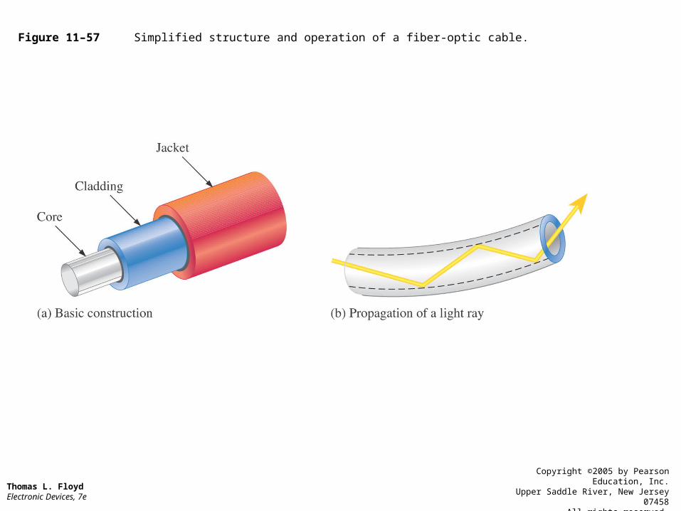
Figure 11–57 Simplified structure and operation of a fiber-optic cable.
Thomas L. Floyd Electronic Devices, 7e
Copyright ©2005 by Pearson Education, Inc.Upper Saddle River, New Jersey 07458
All rights reserved.
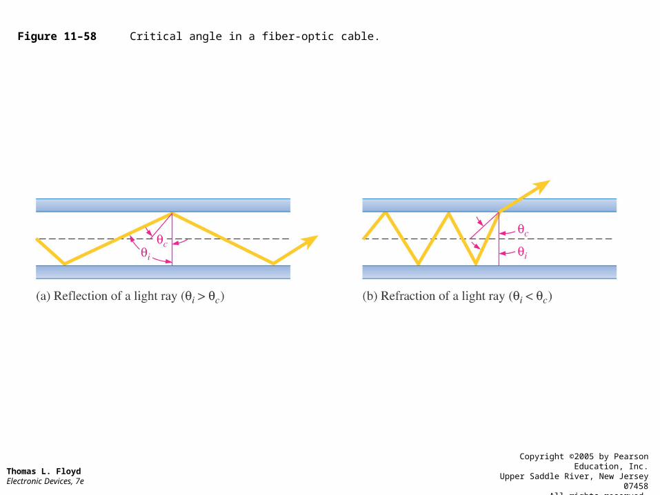
Figure 11–58 Critical angle in a fiber-optic cable.
Thomas L. Floyd Electronic Devices, 7e
Copyright ©2005 by Pearson Education, Inc.Upper Saddle River, New Jersey 07458
All rights reserved.
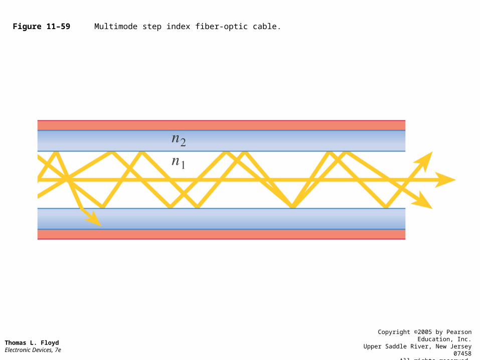
Figure 11–59 Multimode step index fiber-optic cable.
Thomas L. Floyd Electronic Devices, 7e
Copyright ©2005 by Pearson Education, Inc.Upper Saddle River, New Jersey 07458
All rights reserved.
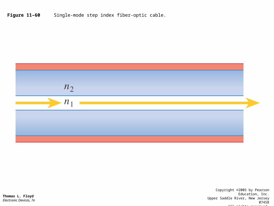
Figure 11–60 Single-mode step index fiber-optic cable.
Thomas L. Floyd Electronic Devices, 7e
Copyright ©2005 by Pearson Education, Inc.Upper Saddle River, New Jersey 07458
All rights reserved.
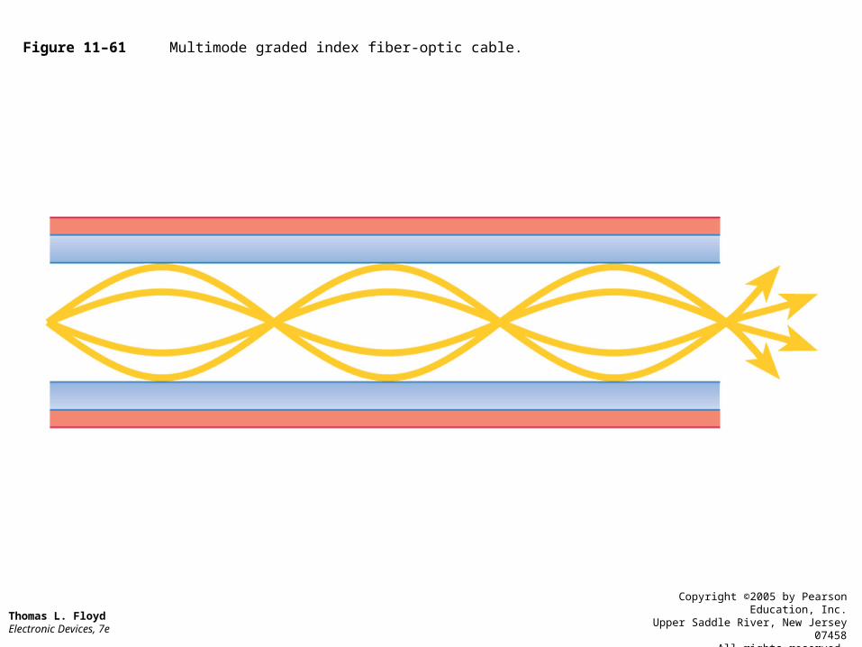
Figure 11–61 Multimode graded index fiber-optic cable.
Thomas L. Floyd Electronic Devices, 7e
Copyright ©2005 by Pearson Education, Inc.Upper Saddle River, New Jersey 07458
All rights reserved.
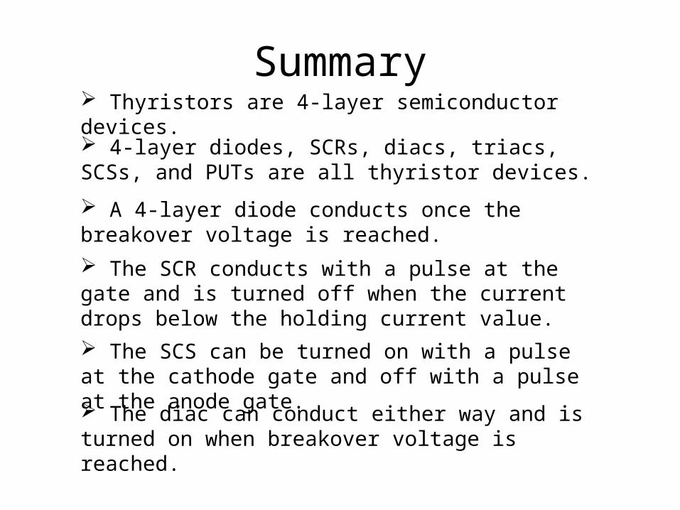
Summary Thyristors are 4-layer semiconductor devices.
4-layer diodes, SCRs, diacs, triacs, SCSs, and PUTs are all thyristor devices.
The SCR conducts with a pulse at the gate and is turned off when the current drops below the holding current value. The SCS can be turned on with a pulse at the cathode gate and off with a pulse at the anode gate.
A 4-layer diode conducts once the breakover voltage is reached.
The diac can conduct either way and is turned on when breakover voltage is reached.
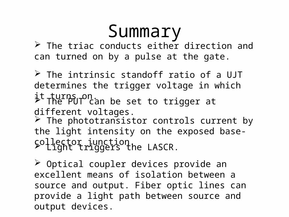
Summary The triac conducts either direction and can turned on by a pulse at the gate.
The intrinsic standoff ratio of a UJT determines the trigger voltage in which it turns on.
The PUT can be set to trigger at different voltages. The phototransistor controls current by the light intensity on the exposed base-collector junction. Light triggers the LASCR.
Optical coupler devices provide an excellent means of isolation between a source and output. Fiber optic lines can provide a light path between source and output devices.
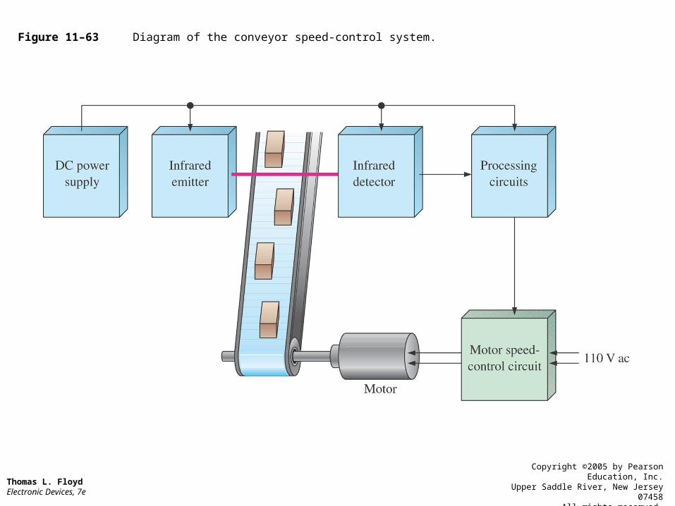
Figure 11–63 Diagram of the conveyor speed-control system.
Thomas L. Floyd Electronic Devices, 7e
Copyright ©2005 by Pearson Education, Inc.Upper Saddle River, New Jersey 07458
All rights reserved.
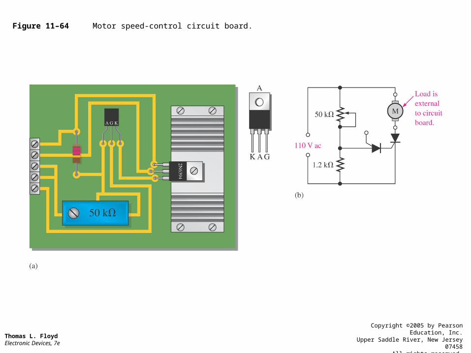
Figure 11–64 Motor speed-control circuit board.
Thomas L. Floyd Electronic Devices, 7e
Copyright ©2005 by Pearson Education, Inc.Upper Saddle River, New Jersey 07458
All rights reserved.
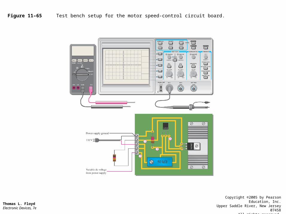
Figure 11–65 Test bench setup for the motor speed-control circuit board.
Thomas L. Floyd Electronic Devices, 7e
Copyright ©2005 by Pearson Education, Inc.Upper Saddle River, New Jersey 07458
All rights reserved.
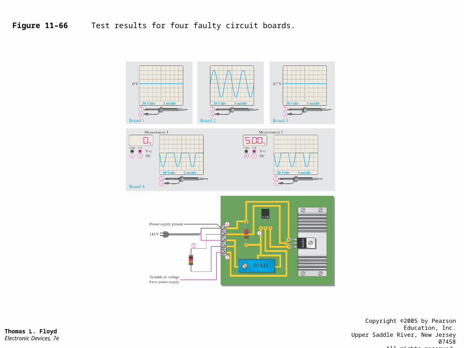
Figure 11–66 Test results for four faulty circuit boards.
Thomas L. Floyd Electronic Devices, 7e
Copyright ©2005 by Pearson Education, Inc.Upper Saddle River, New Jersey 07458
All rights reserved.
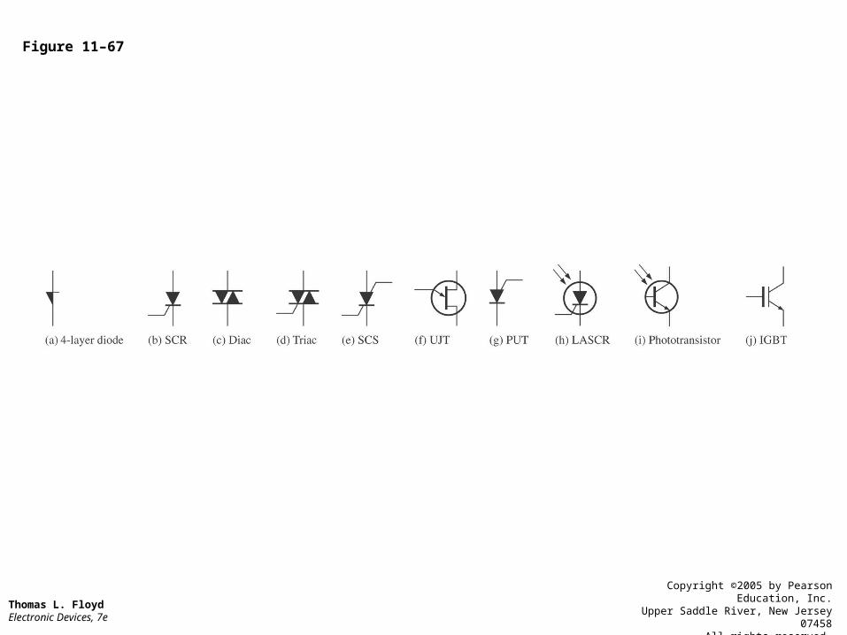
Figure 11–67
Thomas L. Floyd Electronic Devices, 7e
Copyright ©2005 by Pearson Education, Inc.Upper Saddle River, New Jersey 07458
All rights reserved.
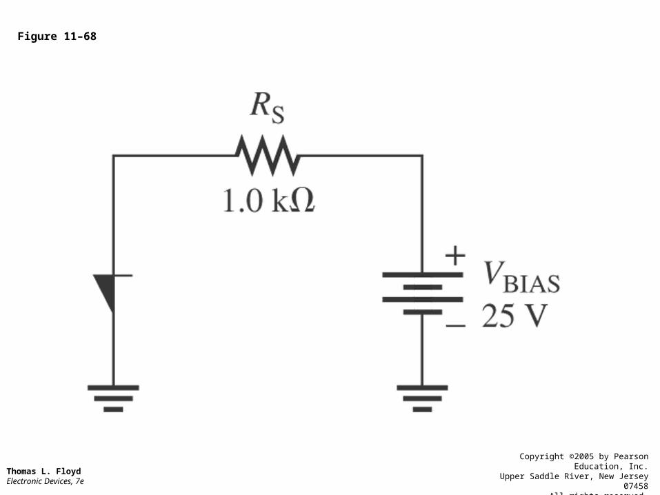
Figure 11–68
Thomas L. Floyd Electronic Devices, 7e
Copyright ©2005 by Pearson Education, Inc.Upper Saddle River, New Jersey 07458
All rights reserved.
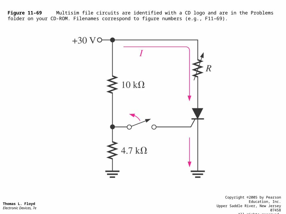
Figure 11–69 Multisim file circuits are identified with a CD logo and are in the Problems folder on your CD-ROM. Filenames correspond to figure numbers (e.g., F11–69).
Thomas L. Floyd Electronic Devices, 7e
Copyright ©2005 by Pearson Education, Inc.Upper Saddle River, New Jersey 07458
All rights reserved.
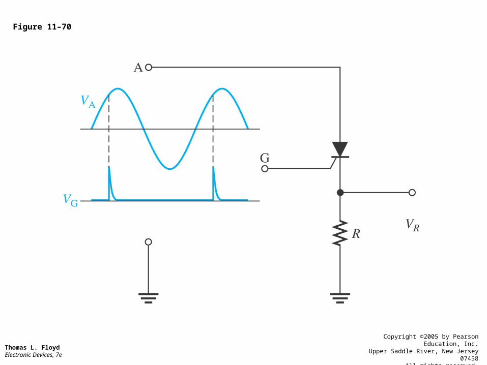
Figure 11–70
Thomas L. Floyd Electronic Devices, 7e
Copyright ©2005 by Pearson Education, Inc.Upper Saddle River, New Jersey 07458
All rights reserved.
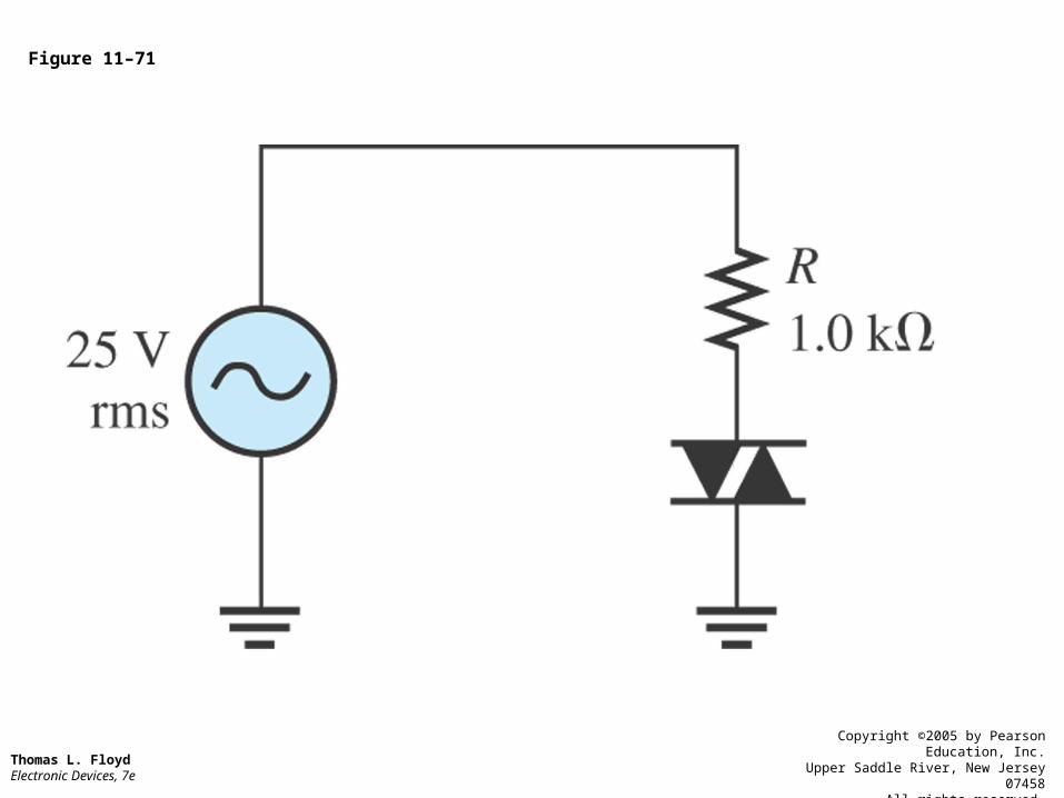
Figure 11–71
Thomas L. Floyd Electronic Devices, 7e
Copyright ©2005 by Pearson Education, Inc.Upper Saddle River, New Jersey 07458
All rights reserved.
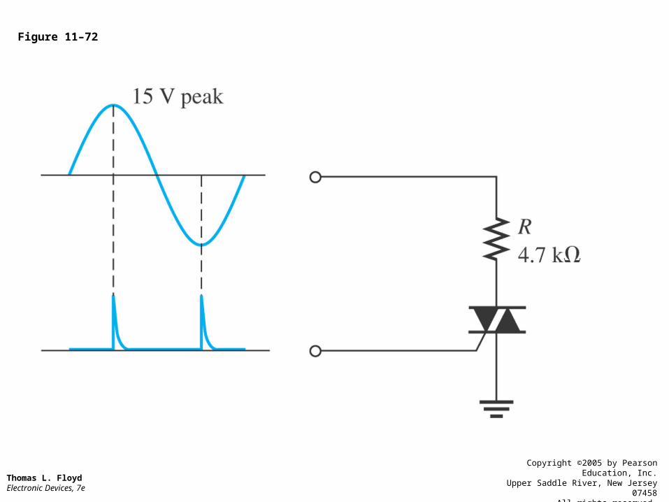
Figure 11–72
Thomas L. Floyd Electronic Devices, 7e
Copyright ©2005 by Pearson Education, Inc.Upper Saddle River, New Jersey 07458
All rights reserved.
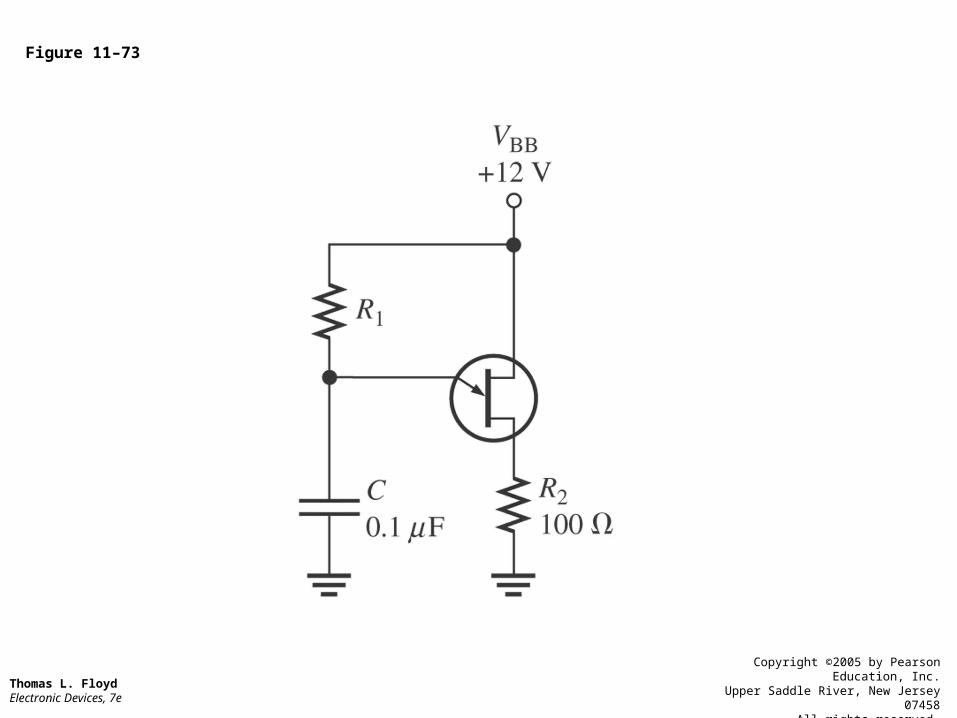
Figure 11–73
Thomas L. Floyd Electronic Devices, 7e
Copyright ©2005 by Pearson Education, Inc.Upper Saddle River, New Jersey 07458
All rights reserved.
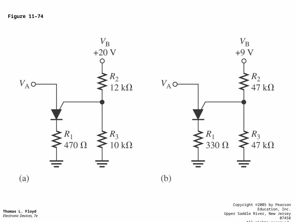
Figure 11–74
Thomas L. Floyd Electronic Devices, 7e
Copyright ©2005 by Pearson Education, Inc.Upper Saddle River, New Jersey 07458
All rights reserved.
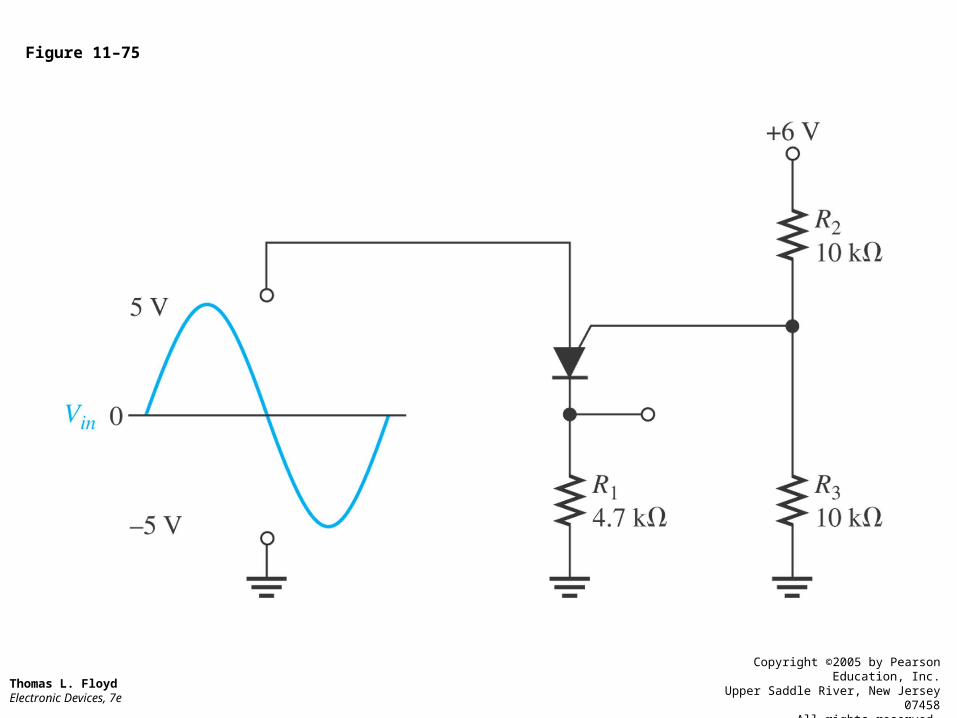
Figure 11–75
Thomas L. Floyd Electronic Devices, 7e
Copyright ©2005 by Pearson Education, Inc.Upper Saddle River, New Jersey 07458
All rights reserved.
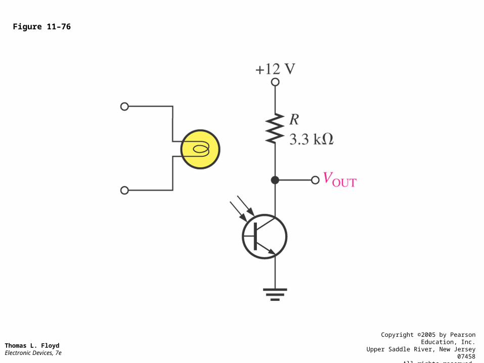
Figure 11–76
Thomas L. Floyd Electronic Devices, 7e
Copyright ©2005 by Pearson Education, Inc.Upper Saddle River, New Jersey 07458
All rights reserved.
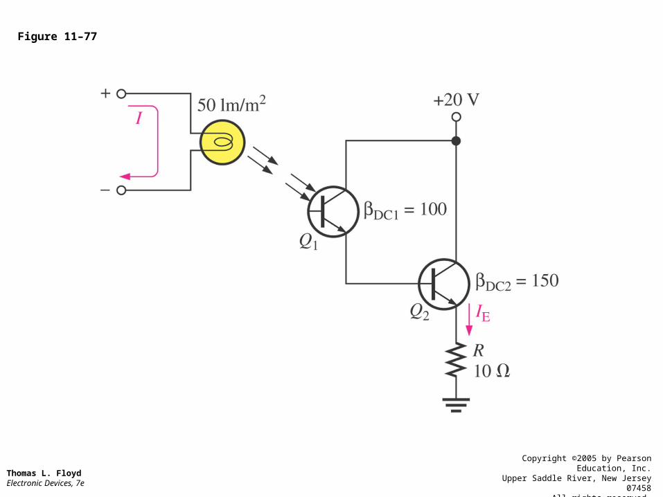
Figure 11–77
Thomas L. Floyd Electronic Devices, 7e
Copyright ©2005 by Pearson Education, Inc.Upper Saddle River, New Jersey 07458
All rights reserved.
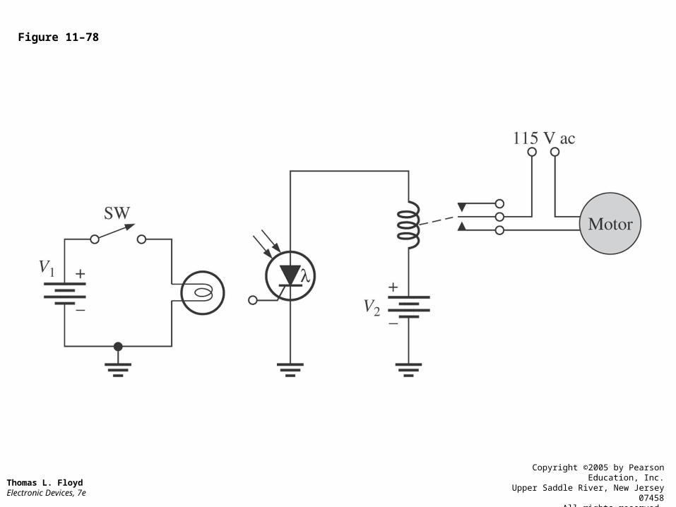
Figure 11–78
Thomas L. Floyd Electronic Devices, 7e
Copyright ©2005 by Pearson Education, Inc.Upper Saddle River, New Jersey 07458
All rights reserved.
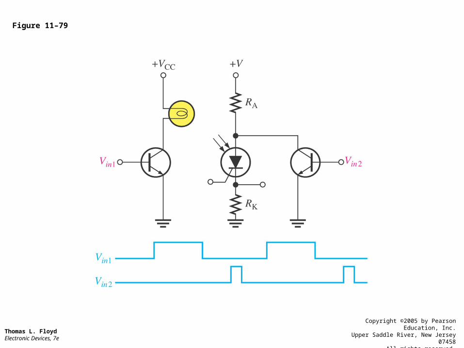
Figure 11–79
Thomas L. Floyd Electronic Devices, 7e
Copyright ©2005 by Pearson Education, Inc.Upper Saddle River, New Jersey 07458
All rights reserved.
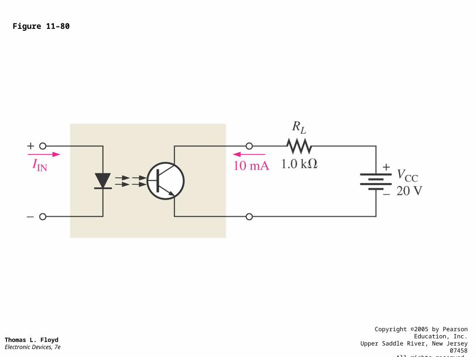
Figure 11–80
Thomas L. Floyd Electronic Devices, 7e
Copyright ©2005 by Pearson Education, Inc.Upper Saddle River, New Jersey 07458
All rights reserved.


