Embed Size (px)
Citation preview

Channel operating margin for PAM4
CDAUI-8 chip-to-chip interfaces
Adam Healey
Avago Technologies
IEEE P802.3bs 400 GbE Task Force
March 2015
2
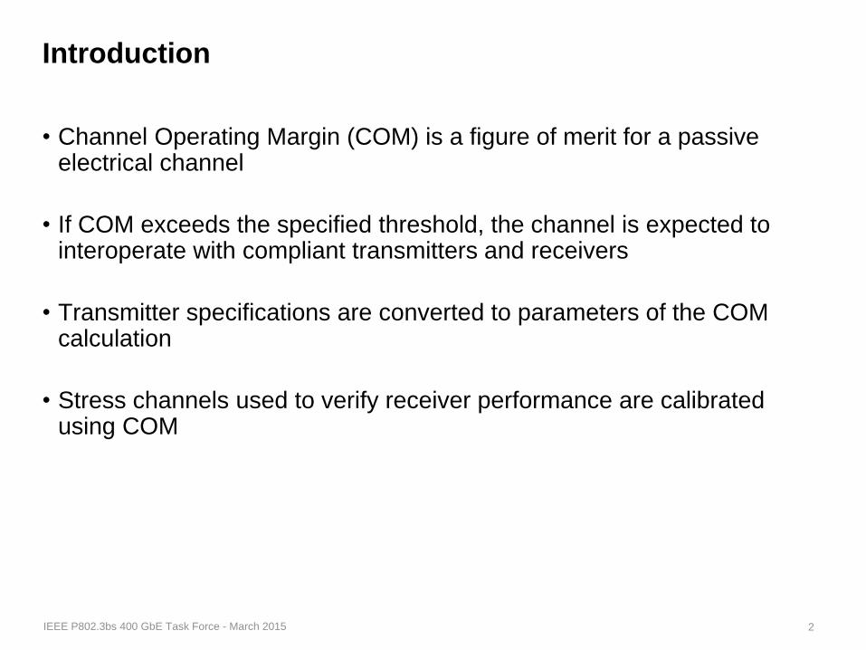
Introduction
• Channel Operating Margin (COM) is a figure of merit for a passive electrical channel
• If COM exceeds the specified threshold, the channel is expected to interoperate with compliant transmitters and receivers
• Transmitter specifications are converted to parameters of the COM calculation
• Stress channels used to verify receiver performance are calibrated using COM
IEEE P802.3bs 400 GbE Task Force - March 2015

3
Words of caution
• A COM value is not a demonstration of feasibility (or lack thereof)
• Transmitters must be able to satisfy the requirements implied by the COM parameters
• Receivers must be able to tolerate the stress implied by the minimum COM
• The reference receiver employed by COM is not an implementation guide
– Enable innovation so long as the performance requirements are met
IEEE P802.3bs 400 GbE Task Force - March 2015
4
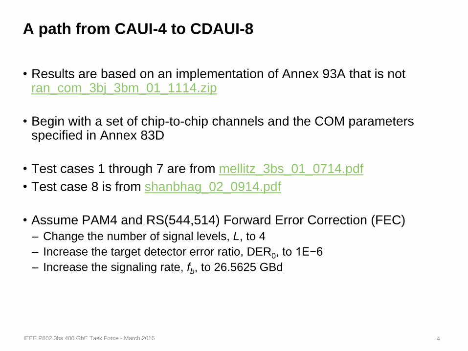
A path from CAUI-4 to CDAUI-8
• Results are based on an implementation of Annex 93A that is not ran_com_3bj_3bm_01_1114.zip
• Begin with a set of chip-to-chip channels and the COM parameters specified in Annex 83D
• Test cases 1 through 7 are from mellitz_3bs_01_0714.pdf
• Test case 8 is from shanbhag_02_0914.pdf
• Assume PAM4 and RS(544,514) Forward Error Correction (FEC)
– Change the number of signal levels, L, to 4
– Increase the target detector error ratio, DER0, to 1E−6
– Increase the signaling rate, fb, to 26.5625 GBd
IEEE P802.3bs 400 GbE Task Force - March 2015

5
Results, first pass
IEEE P802.3bs 400 GbE Task Force - March 2015
Test case 1 2 3 4 5 6 7 8
mellitz_3bs_01_0714.pdf 2.01 2.78 3.06 2.01 2.18 2.95 3.02 n/a
This implementation, zp = 12 mm 3.20 3.70 3.24 3.23 3.13 3.73 3.42 4.77
This implementation, zp = 30 mm 2.00 2.77 3.00 2.03 2.09 2.95 2.86 3.11
Change L to 4, zp = 30 mm −6.39 −5.67 −5.33 −6.36 −6.27 −5.45 −5.46 −5.46
Add RS(544,514), zp = 30 mm −3.55 −2.91 −2.78 −3.58 −3.24 −2.65 −2.74 −2.79
• Inter-symbol interference (ISI)
• Transmitter noise (TXN)
• Uncorrelated jitter (UJN)
Top impairments
6
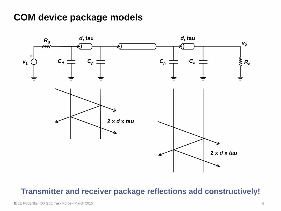
COM device package models
IEEE P802.3bs 400 GbE Task Force - March 2015
Cd Cp
Rd d, tau
v1
Transmitter and receiver package reflections add constructively!
2 x d x tau
2 x d x tau
Rd
d, tau
Cp Cd
v2

7
Influence of COM device package models
IEEE P802.3bs 400 GbE Task Force - March 2015
2 x (12 mm) x (6.14 ps/mm) ~ 3.9 UI 2 x (30 mm) x (6.14 ps/mm) ~ 9.8 UI
zp = 12 mm zp = 30 mm
8
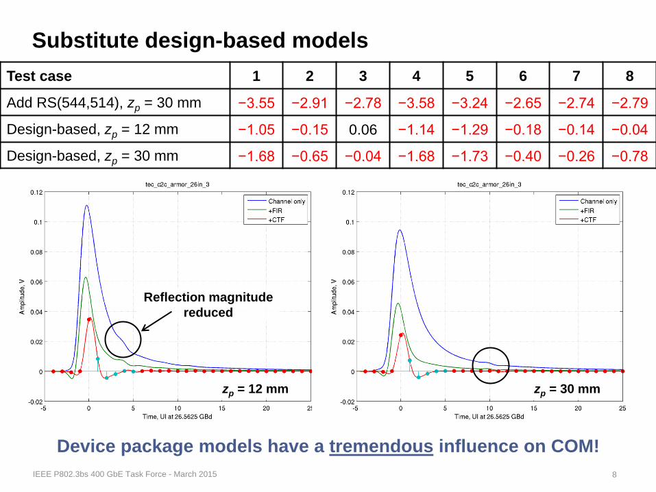
Substitute design-based models
IEEE P802.3bs 400 GbE Task Force - March 2015
Test case 1 2 3 4 5 6 7 8
Add RS(544,514), zp = 30 mm −3.55 −2.91 −2.78 −3.58 −3.24 −2.65 −2.74 −2.79
Design-based, zp = 12 mm −1.05 −0.15 0.06 −1.14 −1.29 −0.18 −0.14 −0.04
Design-based, zp = 30 mm −1.68 −0.65 −0.04 −1.68 −1.73 −0.40 −0.26 −0.78
Device package models have a tremendous influence on COM!
Reflection magnitude
reduced
zp = 12 mm zp = 30 mm

9
Transmitter noise and jitter
• Reduce peak dual-Dirac jitter, ADD, to 0.02 UI
• Increase transmitter signal-to-noise ratio, SNRTX, to 31 dB
• SNRTX represents the signal-to-noise-and-distortion ratio (SNDR) requirement imposed on the transmitter
• SNDR includes linear fit error (distortion) and uncorrelated noise
• SNRTX defines an additive Gaussian noise source based on the SNDR value
• This could result in a conservative COM value
IEEE P802.3bs 400 GbE Task Force - March 2015

10
What is the problem?
• In principle, the transmitter modeled by COM should meet all of the transmitter requirements
– Balancing on the “edge of compliance” to the largest extent possible
• SNRTX = SNDR can result in a non-compliant transmitter model
– A component of SNDR is linear fit error which includes residual ISI
– In this context, “residual” implies ISI outside of an exception window
– The exception window is typically set to equal the DFE length (Np = Nb)
– E.g., if Np = 5 then reflections 10 UI from the main cursor degrade SNDR
• The noise is presumably added to the waveform and impacts both sampling and transition times
– Noise is converted to jitter via the slope of the waveform at the crossing
– However, the model also defines a timing error based on the worst-case uncorrelated jitter
– By definition, the jitter measured at the crossing times will then be larger than allowed
IEEE P802.3bs 400 GbE Task Force - March 2015

11
Path forward for transmitter noise and jitter
• In general, SNRTX should be greater than or equal to SNDR
• SNRTX should be pro-rated by the residual ISI corresponding to the device package model and specified exception window
• Any correction may be applied to the COM parameters or used as a justification to reduce the transmitter SNDR requirement
• Consider reducing the RMS random jitter parameter, sRJ, to account for the jitter induced by the SNRTX noise source
IEEE P802.3bs 400 GbE Task Force - March 2015
12
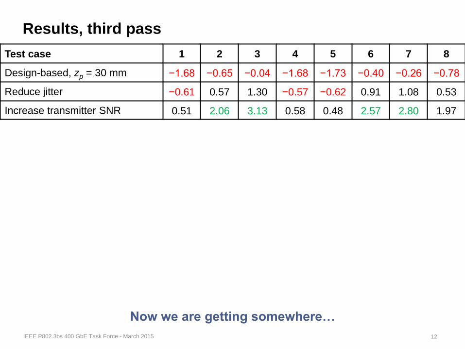
Results, third pass
IEEE P802.3bs 400 GbE Task Force - March 2015
Test case 1 2 3 4 5 6 7 8
Design-based, zp = 30 mm −1.68 −0.65 −0.04 −1.68 −1.73 −0.40 −0.26 −0.78
Reduce jitter −0.61 0.57 1.30 −0.57 −0.62 0.91 1.08 0.53
Increase transmitter SNR 0.51 2.06 3.13 0.58 0.48 2.57 2.80 1.97
Now we are getting somewhere…

13
Equalization
• Increase de-emphasis range of the continuous time filter by 3 dB
– gDC from −15 to 0 dB in 1 dB steps
• For CAUI-4, decision feedback equalizer (DFE) coefficients were constrained to limit error propagation
• CDAUI-8 is assumed to leverage RS(544,514) or a similar code
• Adopt the 100GBASE-KP4 coefficient constraints
– bmax(1) = 1, otherwise bmax(n) = 0.2
IEEE P802.3bs 400 GbE Task Force - March 2015

14
Results, final pass
• Level separation mismatch ratio corresponds to a significant penalty
• E.g., tightening requirement from 0.92 to 0.95 yields COM+0.28 dB
– However, more data is needed to justify a change
IEEE P802.3bs 400 GbE Task Force - March 2015
Test case 1 2 3 4 5 6 7 8
Increase transmitter SNR 0.51 2.06 3.13 0.58 0.48 2.57 2.80 1.97
Increase gDC range 1.14 2.54 3.13 0.72 0.86 2.76 2.81 2.58
Relax DFE constraints 1.88 2.94 3.13 1.81 1.37 2.76 2.81 2.92
Reduce level separation 1.16 2.22 2.41 1.09 0.65 2.04 2.09 2.20
A number of interesting channels show greater than 2 dB margin
15
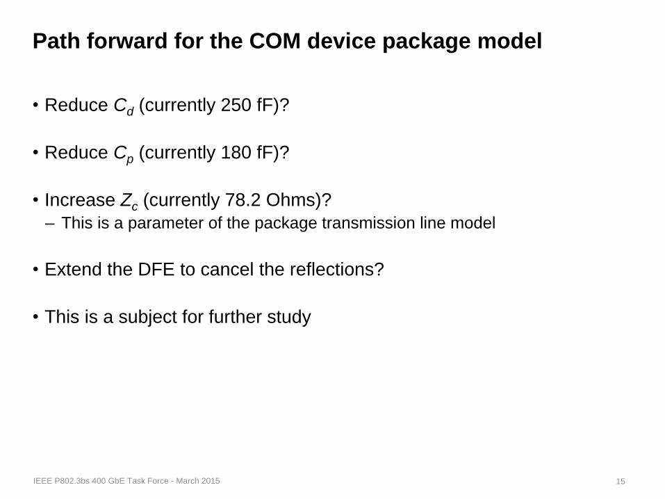
Path forward for the COM device package model
• Reduce Cd (currently 250 fF)?
• Reduce Cp (currently 180 fF)?
• Increase Zc (currently 78.2 Ohms)?
– This is a parameter of the package transmission line model
• Extend the DFE to cancel the reflections?
• This is a subject for further study
IEEE P802.3bs 400 GbE Task Force - March 2015
16
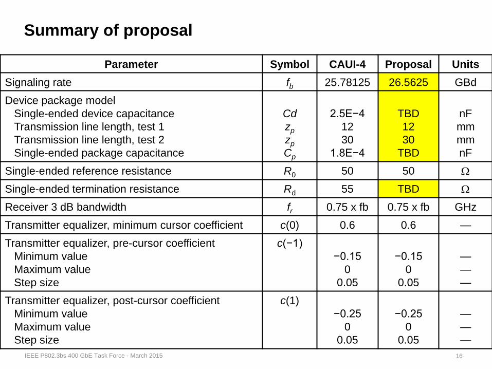
Summary of proposal
IEEE P802.3bs 400 GbE Task Force - March 2015
Parameter Symbol CAUI-4 Proposal Units
Signaling rate fb 25.78125 26.5625 GBd
Device package model
Single-ended device capacitance
Transmission line length, test 1
Transmission line length, test 2
Single-ended package capacitance
Cd
zp
zp
Cp
2.5E−4
12
30
1.8E−4
TBD
12
30
TBD
nF
mm
mm
nF
Single-ended reference resistance R0 50 50 W
Single-ended termination resistance Rd 55 TBD W
Receiver 3 dB bandwidth fr 0.75 x fb 0.75 x fb GHz
Transmitter equalizer, minimum cursor coefficient c(0) 0.6 0.6 —
Transmitter equalizer, pre-cursor coefficient
Minimum value
Maximum value
Step size
c(−1)
−0.15
0
0.05
−0.15
0
0.05
—
—
—
Transmitter equalizer, post-cursor coefficient
Minimum value
Maximum value
Step size
c(1)
−0.25
0
0.05
−0.25
0
0.05
—
—
—
17
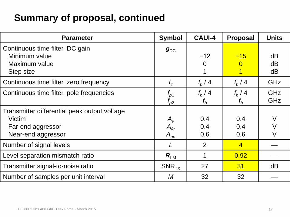
Summary of proposal, continued
IEEE P802.3bs 400 GbE Task Force - March 2015
Parameter Symbol CAUI-4 Proposal Units
Continuous time filter, DC gain
Minimum value
Maximum value
Step size
gDC
−12
0
1
−15
0
1
dB
dB
dB
Continuous time filter, zero frequency fz fb / 4 fb / 4 GHz
Continuous time filter, pole frequencies fp1
fp2
fb / 4
fb
fb / 4
fb
GHz
GHz
Transmitter differential peak output voltage
Victim
Far-end aggressor
Near-end aggressor
Av
Afe
Ane
0.4
0.4
0.6
0.4
0.4
0.6
V
V
V
Number of signal levels L 2 4 —
Level separation mismatch ratio RLM 1 0.92 —
Transmitter signal-to-noise ratio SNRTX 27 31 dB
Number of samples per unit interval M 32 32 —

18
Summary of proposal, continued
IEEE P802.3bs 400 GbE Task Force - March 2015
Parameter Symbol CAUI-4 Proposal Units
Decision feedback equalizer (DFE) length Nb 5 5 UI
Normalized DFE coefficient magnitude limit
n = 1
n = 2 to Nb
bmax(n)
0.3
0.3
1.0
0.2
—
—
Random jitter, RMS sRJ 0.01 0.01 UI
Dual-Dirac jitter, peak ADD 0.05 0.02 UI
One-sided noise spectral density h0 5.2E−8 5.2E−8 V2/GHz
Target detector error ratio DER0 1E−15 1E−6 —
Channel operating margin, min. COM 2 2 dB

19
Key take-aways
• Device package models have a large influence on COM
• Design-based package models yield significantly higher COM values
• Transmitter noise and jitter parameters must be properly calibrated to avoid worse than worst-case modeling and hidden margin
• This proposal yields COM values greater than 2 dB for a multiple chip-to-chip channels given appropriate adjustments to the device package models
• Additional enhancements will be investigated
IEEE P802.3bs 400 GbE Task Force - March 2015