Embed Size (px)
Citation preview
1
CHAPTER 1
REVIEW AND PREPARATION OF DILUTED
MAGNETIC SEMICONDUCTORS
1.1 REVIEW OF DILUTED MAGNETIC SEMICONDUCTORS
Diluted magnetic semiconductors (DMS) are referred as
semimagnetic semiconductors, with lattice partly substituted by magnetic
atoms. In semiconductor devices, the information is transferred by charge
carriers and in contrast, magnetic materials are utilized on the basis of
electron spin in DMS. In order to develop multi functional devices, it is
essential to combine both charge and spin of the electrons. In this, the spin of
electrons that carries the information can be used as an added degree of
freedom in novel electronic devices (Wolf et al 2001). Thus the emerging
research area known as ‘spintronics’ or spin based electronics seeks to extend
the properties and applications of established devices by making use of the
spin of electrons in addition to their charge (Das Sarma 2001). It is possible to
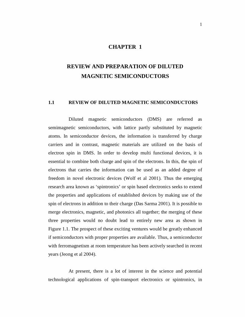
merge electronics, magnetic, and photonics all together; the merging of these
three properties would no doubt lead to entirely new area as shown in
Figure 1.1. The prospect of these exciting ventures would be greatly enhanced
if semiconductors with proper properties are available. Thus, a semiconductor
with ferromagnetism at room temperature has been actively searched in recent
years (Jeong et al 2004).
At present, there is a lot of interest in the science and potential
technological applications of spin-transport electronics or spintronics, in
2
which the spin of charge carriers is exploited to provide new functionality for
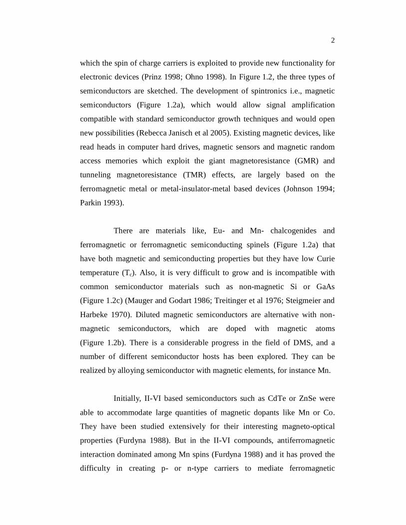
electronic devices (Prinz 1998; Ohno 1998). In Figure 1.2, the three types of
semiconductors are sketched. The development of spintronics i.e., magnetic
semiconductors (Figure 1.2a), which would allow signal amplification
compatible with standard semiconductor growth techniques and would open
new possibilities (Rebecca Janisch et al 2005). Existing magnetic devices, like
read heads in computer hard drives, magnetic sensors and magnetic random
access memories which exploit the giant magnetoresistance (GMR) and
tunneling magnetoresistance (TMR) effects, are largely based on the
ferromagnetic metal or metal-insulator-metal based devices (Johnson 1994;
Parkin 1993).
There are materials like, Eu- and Mn- chalcogenides and
ferromagnetic or ferromagnetic semiconducting spinels (Figure 1.2a) that
have both magnetic and semiconducting properties but they have low Curie
temperature (Tc). Also, it is very difficult to grow and is incompatible with
common semiconductor materials such as non-magnetic Si or GaAs
(Figure 1.2c) (Mauger and Godart 1986; Treitinger et al 1976; Steigmeier and
Harbeke 1970). Diluted magnetic semiconductors are alternative with non-
magnetic semiconductors, which are doped with magnetic atoms
(Figure 1.2b). There is a considerable progress in the field of DMS, and a
number of different semiconductor hosts has been explored. They can be
realized by alloying semiconductor with magnetic elements, for instance Mn.
Initially, II-VI based semiconductors such as CdTe or ZnSe were
able to accommodate large quantities of magnetic dopants like Mn or Co.
They have been studied extensively for their interesting magneto-optical
properties (Furdyna 1988). But in the II-VI compounds, antiferromagnetic
interaction dominated among Mn spins (Furdyna 1988) and it has proved the
difficulty in creating p- or n-type carriers to mediate ferromagnetic
3
Electron Charge
Photonics
Electron Spin
Semiconductor Spintronics
Figure 1.1 Schematic representations of spintronics
Figure 1.2 Three types of magnetic semiconductors a) magnetic
semiconductor, b) diluted magnetic semiconductor, an alloy
between magnetic element and nonmagnetic semiconductor,
c) nonmagnetic semiconductor with no magnetic ions
(a) (b) (c)
4
interaction. Also, the ferromagnetic property was detected at low temperature,
which is not suitable for practical applications. III-V semiconductors such as
GaAs or InAs are more promising for DMS. When divalent transition metal
ions are doped in a trivalent III-V host lattice, holes are also introduced to
mediate the observed ferromagnetic ordering in these systems. The Curie
temperature (Tc) of III-V semiconductors based DMS goes upto ~100 K
which is higher than those of II-VI DMS, but have not reached the room
temperature values that are desirable for device applications (Ohno 1998;
Sanvito et al 2002).
1.1.1 Ferromagnetism in DMS Materials
Oxides based DMS have been reported to be robust room
temperature ferromagnets due to several distinct reasons like, possibility of
tuning the lattice constant and band parameter by varying the composition of
the material, the random distribution of magnetic ions over the cation
sublattice leads to important magnetic effects and large electronegativity of
oxygen is expected to produce strong p-d exchange coupling between band
carriers and localized spins (Mizokawa et al 2002) etc. Among the oxide
based semiconductors, Zinc oxide (ZnO) and Titanium dioxide (TiO2)
systems have received much attention due to the existence of ferromagnetic
property at room temperature. The ferromagnetic property in oxide DMS
materials has been explained by given various models.
Dietl et al (2000) proposed a model called free carrier mediated exchage model and this model was based on the original model of Zener and the Ruderman-Kittel-Kasuya-Yoshida (RKKY) interaction (Fukumura et al 2005; Liu et al 2005). This model explained the ferromagnetism by exchange interaction between carriers and localized spins ie the magnetic property was mediated by the charge carriers of the materials. The transition temperature
5
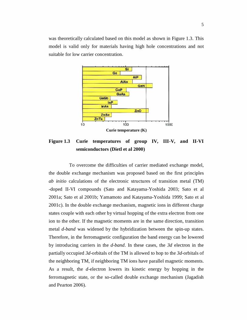
was theoretically calculated based on this model as shown in Figure 1.3. This model is valid only for materials having high hole concentrations and not suitable for low carrier concentration.
Figure 1.3 Curie temperatures of group IV, III-V, and II-VI semiconductors (Dietl et al 2000)
To overcome the difficulties of carrier mediated exchange model, the double exchange mechanism was proposed based on the first principles ab initio calculations of the electronic structures of transition metal (TM) -doped II-VI compounds (Sato and Katayama-Yoshida 2003; Sato et al 2001a; Sato et al 2001b; Yamamoto and Katayama-Yoshida 1999; Sato et al 2001c). In the double exchange mechanism, magnetic ions in different charge states couple with each other by virtual hopping of the extra electron from one ion to the other. If the magnetic moments are in the same direction, transition metal d-band was widened by the hybridization between the spin-up states. Therefore, in the ferromagnetic configuration the band energy can be lowered by introducing carriers in the d-band. In these cases, the 3d electron in the partially occupied 3d-orbitals of the TM is allowed to hop to the 3d-orbitals of the neighboring TM, if neighboring TM ions have parallel magnetic moments. As a result, the d-electron lowers its kinetic energy by hopping in the ferromagnetic state, or the so-called double exchange mechanism (Jagadish and Pearton 2006).
Curie temperature (K)
6
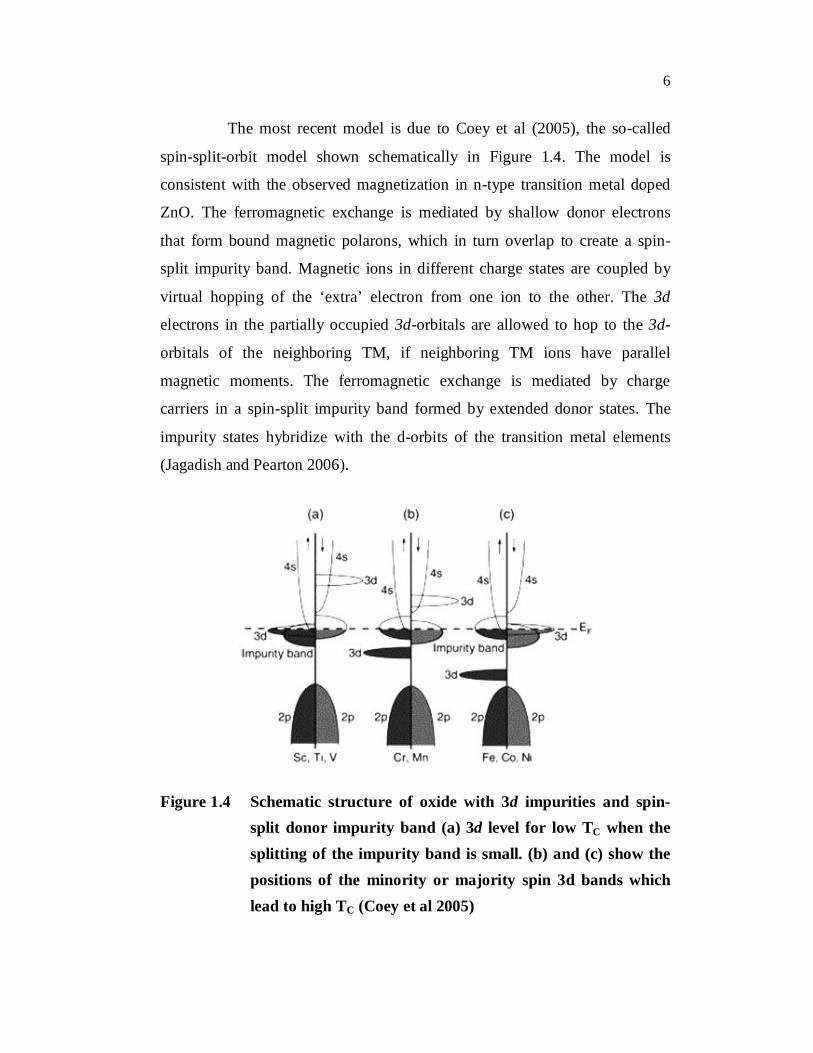
The most recent model is due to Coey et al (2005), the so-called
spin-split-orbit model shown schematically in Figure 1.4. The model is
consistent with the observed magnetization in n-type transition metal doped
ZnO. The ferromagnetic exchange is mediated by shallow donor electrons
that form bound magnetic polarons, which in turn overlap to create a spin-
split impurity band. Magnetic ions in different charge states are coupled by
virtual hopping of the ‘extra’ electron from one ion to the other. The 3d
electrons in the partially occupied 3d-orbitals are allowed to hop to the 3d-
orbitals of the neighboring TM, if neighboring TM ions have parallel
magnetic moments. The ferromagnetic exchange is mediated by charge
carriers in a spin-split impurity band formed by extended donor states. The
impurity states hybridize with the d-orbits of the transition metal elements
(Jagadish and Pearton 2006).
Figure 1.4 Schematic structure of oxide with 3d impurities and spin-split donor impurity band (a) 3d level for low TC when the splitting of the impurity band is small. (b) and (c) show the positions of the minority or majority spin 3d bands which lead to high TC (Coey et al 2005)
7
1.2 BASIC PROPERTIES OF ZnO
Zinc Oxide (ZnO) is a wide band gap (direct) material and presents
an interesting system because of its multidirectional applications e.g. Opto-
electronic displays, electrophotography, photovoltaic conversion and
electroacoustic transducers etc. Its band gap is 3.35 eV at room temperature
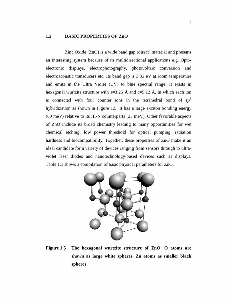
and emits in the Ultra Violet (UV) to blue spectral range. It exists in
hexagonal wurtzite structure with a=3.25 Å and c=5.12 Å, in which each ion
is connected with four counter ions in the tetrahedral bond of sp3
hybridization as shown in Figure 1.5. It has a large exciton bonding energy
(60 meV) relative to its III-N counterparts (25 meV). Other favorable aspects
of ZnO include its broad chemistry leading to many opportunities for wet
chemical etching, low power threshold for optical pumping, radiation
hardness and biocompatibility. Together, these properties of ZnO make it an
ideal candidate for a variety of devices ranging from sensors through to ultra-
violet laser diodes and nanotechnology-based devices such as displays.
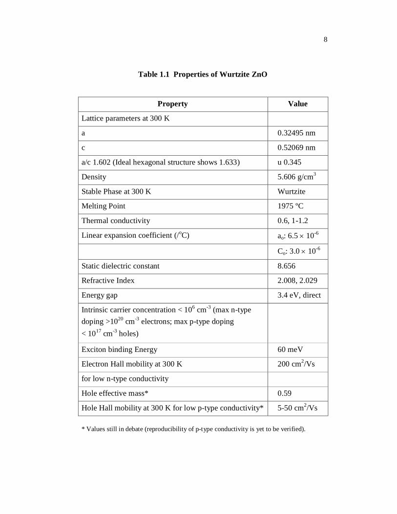
Table 1.1 shows a compilation of basic physical parameters for ZnO.
Figure 1.5 The hexagonal wurtzite structure of ZnO. O atoms are
shown as large white spheres, Zn atoms as smaller black
spheres
8
Table 1.1 Properties of Wurtzite ZnO
Property Value
Lattice parameters at 300 K
a 0.32495 nm
c 0.52069 nm
a/c 1.602 (Ideal hexagonal structure shows 1.633) u 0.345
Density 5.606 g/cm3
Stable Phase at 300 K Wurtzite
Melting Point 1975 ºC
Thermal conductivity 0.6, 1-1.2
Linear expansion coefficient (/oC) ao: 6.5 10-6
Co: 3.0 10-6
Static dielectric constant 8.656
Refractive Index 2.008, 2.029
Energy gap 3.4 eV, direct
Intrinsic carrier concentration < 106 cm-3 (max n-type doping >1020 cm-3 electrons; max p-type doping < 1017 cm-3 holes)
Exciton binding Energy 60 meV
Electron Hall mobility at 300 K 200 cm2/Vs
for low n-type conductivity
Hole effective mass* 0.59
Hole Hall mobility at 300 K for low p-type conductivity* 5-50 cm2/Vs
* Values still in debate (reproducibility of p-type conductivity is yet to be verified).
9
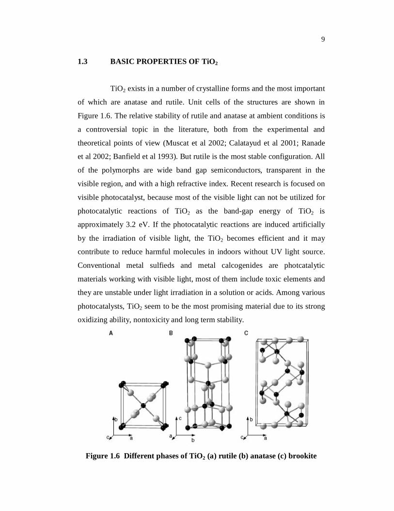
1.3 BASIC PROPERTIES OF TiO2
TiO2 exists in a number of crystalline forms and the most important
of which are anatase and rutile. Unit cells of the structures are shown in
Figure 1.6. The relative stability of rutile and anatase at ambient conditions is
a controversial topic in the literature, both from the experimental and
theoretical points of view (Muscat et al 2002; Calatayud et al 2001; Ranade
et al 2002; Banfield et al 1993). But rutile is the most stable configuration. All
of the polymorphs are wide band gap semiconductors, transparent in the
visible region, and with a high refractive index. Recent research is focused on
visible photocatalyst, because most of the visible light can not be utilized for
photocatalytic reactions of TiO2 as the band-gap energy of TiO2 is
approximately 3.2 eV. If the photocatalytic reactions are induced artificially
by the irradiation of visible light, the TiO2 becomes efficient and it may
contribute to reduce harmful molecules in indoors without UV light source.
Conventional metal sulfieds and metal calcogenides are photcatalytic
materials working with visible light, most of them include toxic elements and
they are unstable under light irradiation in a solution or acids. Among various
photocatalysts, TiO2 seem to be the most promising material due to its strong
oxidizing ability, nontoxicity and long term stability.
Figure 1.6 Different phases of TiO2 (a) rutile (b) anatase (c) brookite
10
1.4 PREPARATION TECHNIQUES
1.4.1 Sol-gel Method
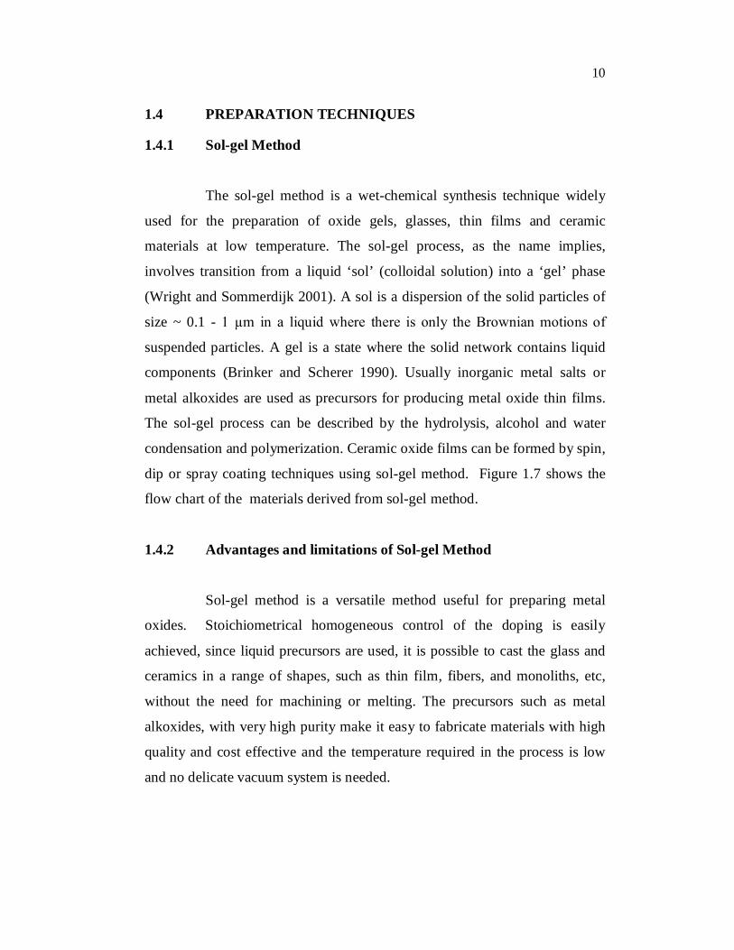
The sol-gel method is a wet-chemical synthesis technique widely
used for the preparation of oxide gels, glasses, thin films and ceramic
materials at low temperature. The sol-gel process, as the name implies,
involves transition from a liquid ‘sol’ (colloidal solution) into a ‘gel’ phase
(Wright and Sommerdijk 2001). A sol is a dispersion of the solid particles of
size ~ 0.1 - 1 µm in a liquid where there is only the Brownian motions of
suspended particles. A gel is a state where the solid network contains liquid
components (Brinker and Scherer 1990). Usually inorganic metal salts or
metal alkoxides are used as precursors for producing metal oxide thin films.
The sol-gel process can be described by the hydrolysis, alcohol and water
condensation and polymerization. Ceramic oxide films can be formed by spin,
dip or spray coating techniques using sol-gel method. Figure 1.7 shows the
flow chart of the materials derived from sol-gel method.
1.4.2 Advantages and limitations of Sol-gel Method
Sol-gel method is a versatile method useful for preparing metal
oxides. Stoichiometrical homogeneous control of the doping is easily
achieved, since liquid precursors are used, it is possible to cast the glass and
ceramics in a range of shapes, such as thin film, fibers, and monoliths, etc,
without the need for machining or melting. The precursors such as metal
alkoxides, with very high purity make it easy to fabricate materials with high
quality and cost effective and the temperature required in the process is low
and no delicate vacuum system is needed.
11
Despite its advantages, sol-gel method still has some limitation.
Sol-gel technique is not widely used in industries due to weak bonding, low
wear-resistance, high permeability and difficulty in controlling the porosity.
Very careful attentions are needed to avoid cracking of the thin films. The
trapped organics with the thick coating often result in failure during thermal
process. The present sol-gel technique is very substrate-dependent, and the
thermal expansion mismatch limits the wide application of sol-gel technique.
1.4.3 Spin Coating Technique
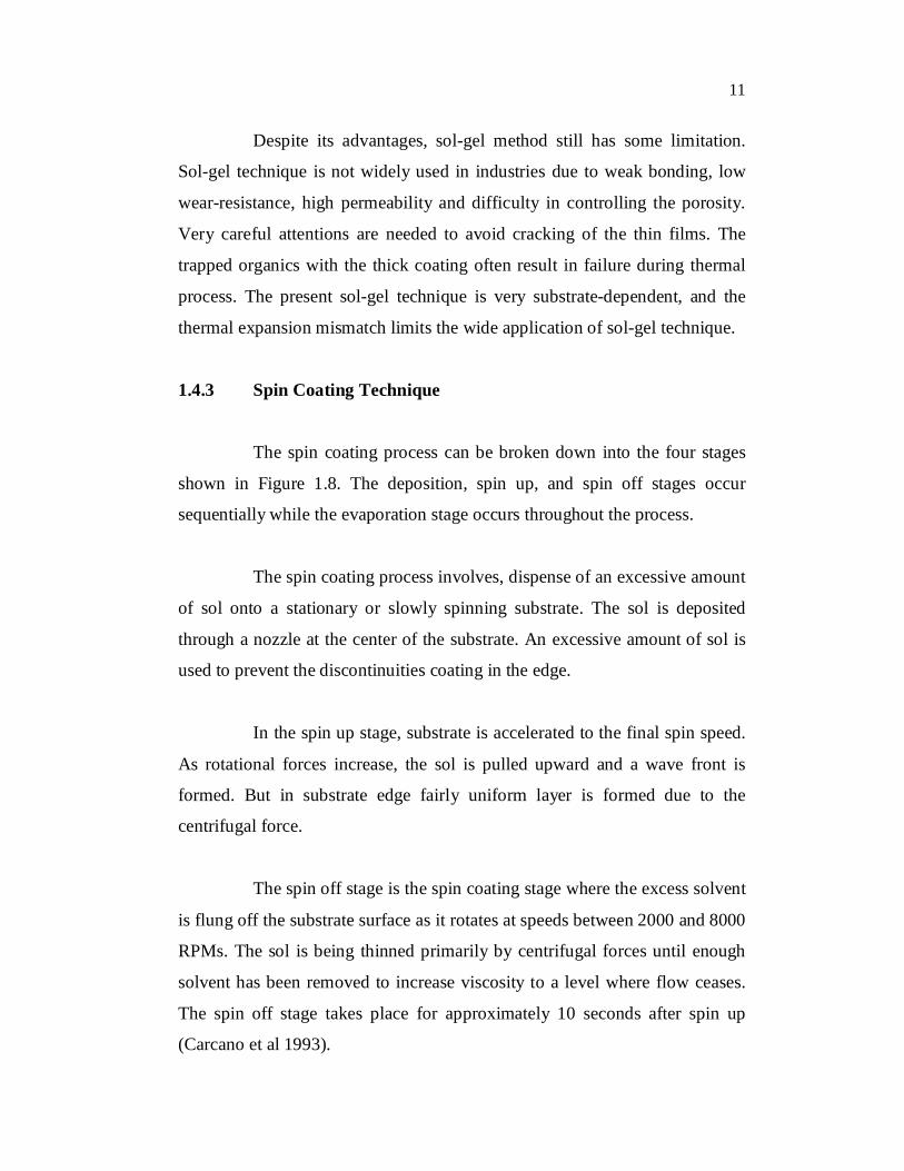
The spin coating process can be broken down into the four stages
shown in Figure 1.8. The deposition, spin up, and spin off stages occur
sequentially while the evaporation stage occurs throughout the process.
The spin coating process involves, dispense of an excessive amount
of sol onto a stationary or slowly spinning substrate. The sol is deposited
through a nozzle at the center of the substrate. An excessive amount of sol is
used to prevent the discontinuities coating in the edge.
In the spin up stage, substrate is accelerated to the final spin speed.
As rotational forces increase, the sol is pulled upward and a wave front is
formed. But in substrate edge fairly uniform layer is formed due to the
centrifugal force.
The spin off stage is the spin coating stage where the excess solvent
is flung off the substrate surface as it rotates at speeds between 2000 and 8000
RPMs. The sol is being thinned primarily by centrifugal forces until enough
solvent has been removed to increase viscosity to a level where flow ceases.
The spin off stage takes place for approximately 10 seconds after spin up
(Carcano et al 1993).
12
Figure 1.7 Flow chart of materials derived from sol-gel process
Figure 1.8 The Four Stages of the Spin Coating Process (Bornside et al
1987)
Sol
Xerogel Film
Dense Film
Gel
Aerogel Xerogel
Dense Ceramic
Fibers
Deposition Spin up
Spin off Evaporation
13
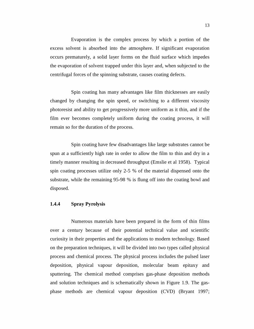
Evaporation is the complex process by which a portion of the
excess solvent is absorbed into the atmosphere. If significant evaporation
occurs prematurely, a solid layer forms on the fluid surface which impedes
the evaporation of solvent trapped under this layer and, when subjected to the
centrifugal forces of the spinning substrate, causes coating defects.
Spin coating has many advantages like film thicknesses are easily
changed by changing the spin speed, or switching to a different viscosity
photoresist and ability to get progressively more uniform as it thin, and if the
film ever becomes completely uniform during the coating process, it will
remain so for the duration of the process.
Spin coating have few disadvantages like large substrates cannot be
spun at a sufficiently high rate in order to allow the film to thin and dry in a
timely manner resulting in decreased throughput (Emslie et al 1958). Typical
spin coating processes utilize only 2-5 % of the material dispensed onto the
substrate, while the remaining 95-98 % is flung off into the coating bowl and
disposed.
1.4.4 Spray Pyrolysis
Numerous materials have been prepared in the form of thin films
over a century because of their potential technical value and scientific
curiosity in their properties and the applications to modern technology. Based
on the preparation techniques, it will be divided into two types called physical
process and chemical process. The physical process includes the pulsed laser
deposition, physical vapour deposition, molecular beam epitaxy and
sputtering. The chemical method comprises gas-phase deposition methods
and solution techniques and is schematically shown in Figure 1.9. The gas-
phase methods are chemical vapour deposition (CVD) (Bryant 1997;
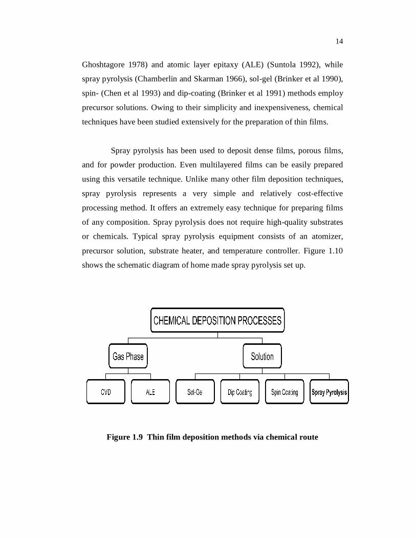
14
Ghoshtagore 1978) and atomic layer epitaxy (ALE) (Suntola 1992), while
spray pyrolysis (Chamberlin and Skarman 1966), sol-gel (Brinker et al 1990),
spin- (Chen et al 1993) and dip-coating (Brinker et al 1991) methods employ
precursor solutions. Owing to their simplicity and inexpensiveness, chemical
techniques have been studied extensively for the preparation of thin films.
Spray pyrolysis has been used to deposit dense films, porous films,
and for powder production. Even multilayered films can be easily prepared
using this versatile technique. Unlike many other film deposition techniques,
spray pyrolysis represents a very simple and relatively cost-effective
processing method. It offers an extremely easy technique for preparing films
of any composition. Spray pyrolysis does not require high-quality substrates
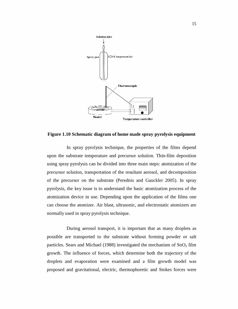
or chemicals. Typical spray pyrolysis equipment consists of an atomizer,
precursor solution, substrate heater, and temperature controller. Figure 1.10
shows the schematic diagram of home made spray pyrolysis set up.
Figure 1.9 Thin film deposition methods via chemical route
15
Figure 1.10 Schematic diagram of home made spray pyrolysis equipment
In spray pyrolysis technique, the properties of the films depend
upon the substrate temperature and precursor solution. Thin-film deposition
using spray pyrolysis can be divided into three main steps: atomization of the
precursor solution, transportation of the resultant aerosol, and decomposition
of the precursor on the substrate (Perednis and Gauckler 2005). In spray
pyrolysis, the key issue is to understand the basic atomization process of the
atomization device in use. Depending upon the application of the films one
can choose the atomizer. Air blast, ultrasonic, and electrostatic atomizers are
normally used in spray pyrolysis technique.
During aerosol transport, it is important that as many droplets as
possible are transported to the substrate without forming powder or salt
particles. Sears and Michael (1988) investigated the mechanism of SnO2 film
growth. The influence of forces, which determine both the trajectory of the
droplets and evaporation were examined and a film growth model was
proposed and gravitational, electric, thermophoretic and Stokes forces were
16
also taken into account. Hsuan-Fu Yu and Wen-Haur Liao (1998) developed a
model describing the evaporation of solution droplets before the formation of
a solid crust and according to his model the transfer of mass, momentum,
temperature outside and around the droplet as well as effects of precursor
precipitation were taken into account. The interactions between droplets were
ignored. Lenggoro et al (2000) investigated powder production by spray
pyrolysis using a temperature-graded laminar flow aerosol reactor and they
calculated the evaporation rate and the change of the precursor concentration
within the droplets. The predicted numerical simulation results were in good
agreement with the experimental results.
Finally in decomposition of the precursor, many processes occur
simultaneously when a droplet hits the surface of the substrate: evaporation of
residual solvent, spreading of the droplet, and salt decomposition. Many
models exist for the decomposition of a precursor and most of the authors
suggest that chemical vapour deposition based process gives high quality
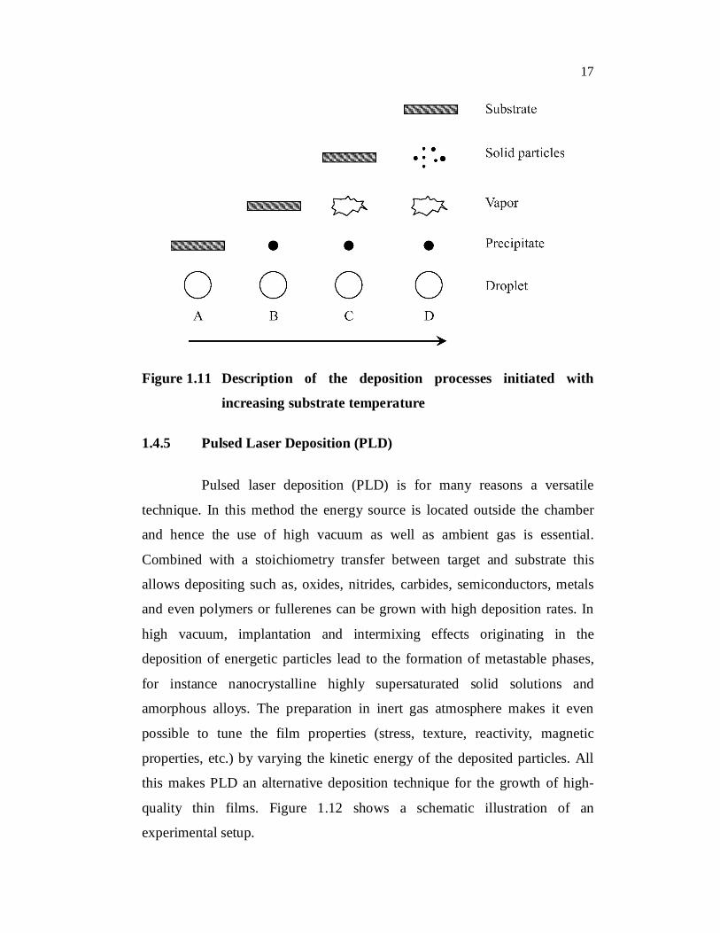
films by spray pyrolysis. Figure 1.11 shows the decomposition of the
precursor when increasing the substrate temperature (Perednis and Gauckler
2005).
Spray pyrolysis is a versatile and effective technique to deposit
metal oxide films. The most important parameter is the substrate temperature
and if the substrate temperature is high then the films are rougher and more
porous. If the temperature is too low, the films will be cracked. Also, the
substrate temperature influences the crystallinity, texture, and other physical
properties of the deposited films. Another important spray parameter is the
precursor solution and it affects the morphology and the properties of the
deposited films. In addition, the film morphology and properties can be
drastically changed by using various additives in the precursor solution
(Perednis and Gauckler 2005).
17
Figure 1.11 Description of the deposition processes initiated with
increasing substrate temperature
1.4.5 Pulsed Laser Deposition (PLD)
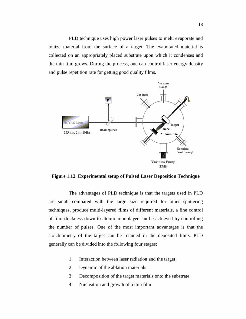
Pulsed laser deposition (PLD) is for many reasons a versatile
technique. In this method the energy source is located outside the chamber
and hence the use of high vacuum as well as ambient gas is essential.
Combined with a stoichiometry transfer between target and substrate this
allows depositing such as, oxides, nitrides, carbides, semiconductors, metals
and even polymers or fullerenes can be grown with high deposition rates. In
high vacuum, implantation and intermixing effects originating in the
deposition of energetic particles lead to the formation of metastable phases,
for instance nanocrystalline highly supersaturated solid solutions and
amorphous alloys. The preparation in inert gas atmosphere makes it even
possible to tune the film properties (stress, texture, reactivity, magnetic
properties, etc.) by varying the kinetic energy of the deposited particles. All
this makes PLD an alternative deposition technique for the growth of high-
quality thin films. Figure 1.12 shows a schematic illustration of an
experimental setup.
18
PLD technique uses high power laser pulses to melt, evaporate and
ionize material from the surface of a target. The evaporated material is
collected on an appropriately placed substrate upon which it condenses and
the thin film grows. During the process, one can control laser energy density
and pulse repetition rate for getting good quality films.
Figure 1.12 Experimental setup of Pulsed Laser Deposition Technique
The advantages of PLD technique is that the targets used in PLD
are small compared with the large size required for other sputtering
techniques, produce multi-layered films of different materials, a fine control
of film thickness down to atomic monolayer can be achieved by controlling
the number of pulses. One of the most important advantages is that the
stoichiometry of the target can be retained in the deposited films. PLD
generally can be divided into the following four stages:
1. Interaction between laser radiation and the target
2. Dynamic of the ablation materials
3. Decomposition of the target materials onto the substrate
4. Nucleation and growth of a thin film
19
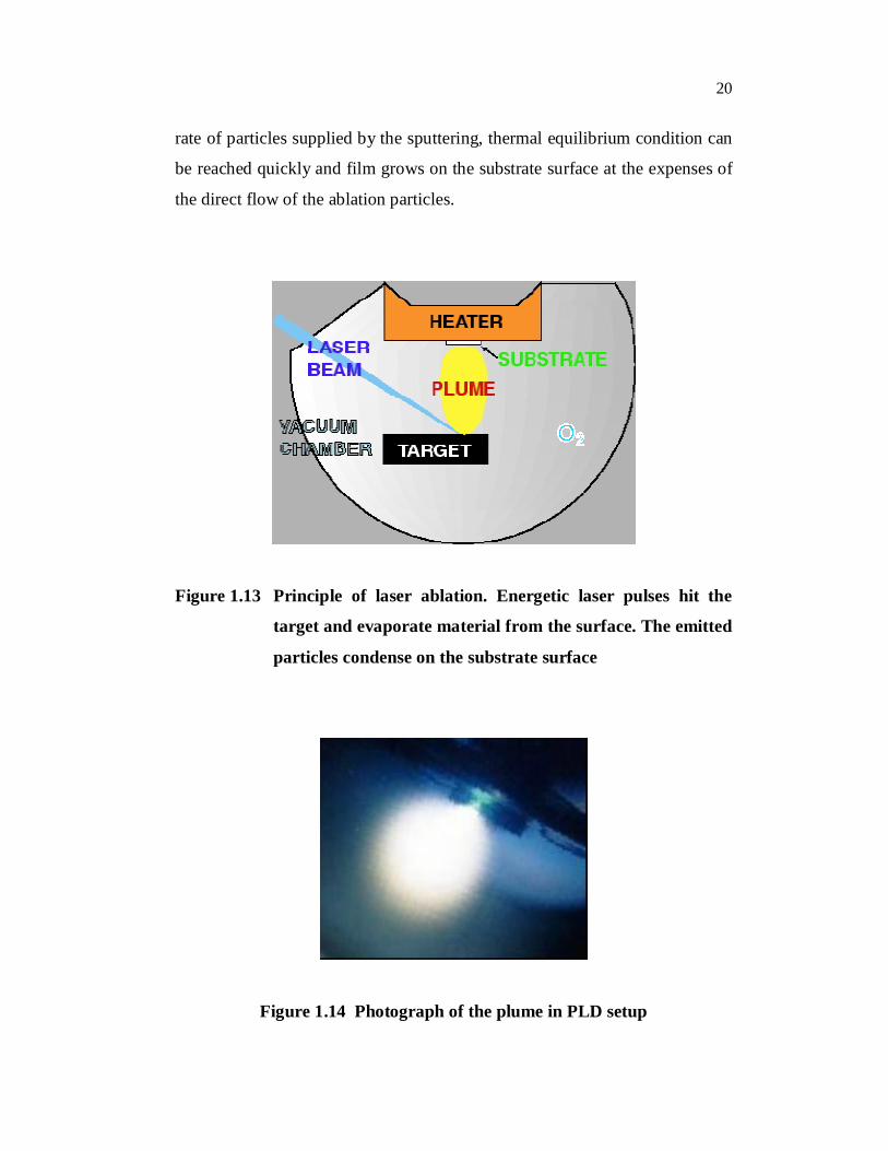
In the first stage, pulsed laser beam is focused on a target and the
laser beam results in a locally very high energy density on the target surface.
The electromagnetic energy is converted into thermal energy via electronic
processes, and results in evaporation of the source material (Chrisey and
Hubler 1994). This process takes place on a very short timescale, shorter than
the laser pulse duration. Extremely high temperatures are reached resulting in
high density plasma that starts to expand due to the pressure gradient close to
the target surface. The instantaneous ablation rate is highly dependent on the
fluences of the laser irradiation on the target. The ablation mechanisms
involve many complex physical phenomena such as collision, thermal and
electronic excitation, exfoliation and hydrodynamics. Figure 1.13 shows the
schematic representation of the laser ablation and Figure 1.14 shows the
photograph of observed plume in PLD setup.
In the second stage, the emitted materials (plume) tend to move
towards the substrate according to the laws of gas-dynamic and show the
forward peaking phenomenon (Namiki et al 1986). The uniformity of the
films can be controlled by controlling the laser spot size and the plasma
temperature. The target-to-substrate distance is another parameter that
governs the angular spread of the ablated materials and Hanabusa (1993)
found a mask placed close to the substrate could reduce the spreading.
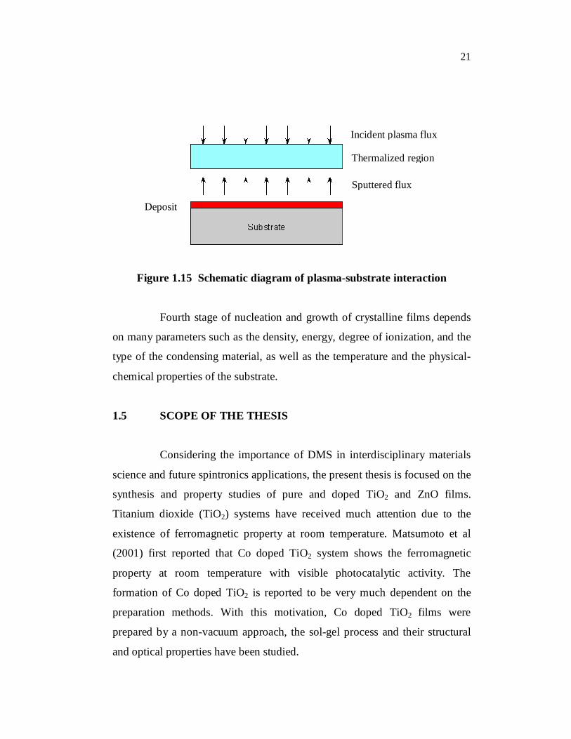
The third stage is important to determine the quality of thin film.
The ejected high-energy species from the target material impinge onto the
substrate surface. The mechanism of the interaction is illustrated in the
following Figure 1.15. The energetic species sputter some of the surface
atoms on the substrate and a collision region is established between the
incident flow and the sputtered atoms. Film grows immediately after this
thermalized region (collision region) is formed. The region serves as a source
for condensation of particles. When the condensation rate is higher than the
20
rate of particles supplied by the sputtering, thermal equilibrium condition can
be reached quickly and film grows on the substrate surface at the expenses of
the direct flow of the ablation particles.
Figure 1.13 Principle of laser ablation. Energetic laser pulses hit the
target and evaporate material from the surface. The emitted
particles condense on the substrate surface
Figure 1.14 Photograph of the plume in PLD setup
21
Figure 1.15 Schematic diagram of plasma-substrate interaction
Fourth stage of nucleation and growth of crystalline films depends
on many parameters such as the density, energy, degree of ionization, and the
type of the condensing material, as well as the temperature and the physical-
chemical properties of the substrate.
1.5 SCOPE OF THE THESIS
Considering the importance of DMS in interdisciplinary materials
science and future spintronics applications, the present thesis is focused on the
synthesis and property studies of pure and doped TiO2 and ZnO films.
Titanium dioxide (TiO2) systems have received much attention due to the
existence of ferromagnetic property at room temperature. Matsumoto et al
(2001) first reported that Co doped TiO2 system shows the ferromagnetic
property at room temperature with visible photocatalytic activity. The
formation of Co doped TiO2 is reported to be very much dependent on the
preparation methods. With this motivation, Co doped TiO2 films were
prepared by a non-vacuum approach, the sol-gel process and their structural
and optical properties have been studied.
Incident plasma flux
Thermalized region
Sputtered flux
Deposit
22
Transition and rare earth metal doped ZnO were predicted as the
promising materials for future spintronics devices (Dietl et al 2000; Potzger et
al 2006). Recently ZnO based system motivated the research in DMS due to
prediction of room temperature ferromagnetism in p-type Mn doped ZnO
(Dietl et al 2000). To explore the origin of the ferromagnetism arising due to
the valance state of Mn, the Mn doped ZnO was prepared by spray pyrolysis
and detailed studies on structural, magnetic and optical properties have been
carried out. Ferromagnetism has also been observed in Gd and Nd doped ZnO
(Potzger et al 2006, Mariana Ungureanu et al 2007). In the present study Gd
and Nd doped ZnO thin films have been prepared by spray pyrolysis and the
properties are investigated in detail. It is a challenge to achieve highly
conducting transition metal doped ZnO films without degrading their
magnetic properties, as substitution of transition metal often leads to an
increase in resistivity of films. With this motivation, thin films of
Zn0.95Mn0.05O and Zn0.95Co0.05O with codoping of Ga were prepared by PLD
and their structural, optical and magnetotransport properties have been
studied.
The shift heavy ion (SHI) irradiation has been widely used for
modifications of physical properties of various materials. In this investigation,
Mn doped ZnO films were irradiated with heavy ions like oxygen and nickel
and the effect of irradiation on the structural and optical properties.


![INAS 342 - the Flying Sentinels [Indian Navy]](https://img.pdfslide.net/doc/110x75/577d1cf51a28ab4e1e8b4993/inas-342-the-flying-sentinels-indian-navy.jpg)