Embed Size (px)
Citation preview

1
University of Wisconsin - MadisonECE/Comp Sci 352 Digital Systems FundamentalsKewal K. Saluja and Yu Hen Hu Spring 2002
Chapter 3 – Part 2
Combinational Logic Design
Originals by: Charles R. Kime and Tom Kamisnski
Modified for course use by: Kewal K. Saluja and Yu Hen Hu
© 2001 Prentice Hall, Inc
Logic and Computer Design Fundamentals
Logic and Computer Design Fundamentals© 2001 Prentice Hall, Inc
Chapter 3-2 2
Functional Blocks: Addition
§ Binary addition occurs frequently in digital and computer systems.§ In this section, we:
• Develop a Half-Adder (HA), a 2-input bit-wise addition functional block,
• Develop a Full-Adder (FA), a 3-input bit-wise addition functional block,
• Iterate full-adders using a ripple-carry to perform parallel binary addition, and
• Develop a Carry-Look-Ahead Adder CLA to improve performance.

2
Logic and Computer Design Fundamentals© 2001 Prentice Hall, Inc
Chapter 3-2 3
Functional Block: Half-Adder
§ A 2-input, 1-bit width binary adder that produces the following values:
§ A half adder adds two bits to produce a two-bit sum.§ The sum is expressed as a
sum bit , S and a carry bit, C.§ The half adder can be specified
as a combined truth table for S and C: ⇒
X 0 0 1 1
+ Y + 0 + 1 + 0 + 1
C S 0 0 0 1 0 1 1 0
X Y C S
0 0 0 00 1 0 11 0 0 1
1 1 1 0
Logic and Computer Design Fundamentals© 2001 Prentice Hall, Inc
Chapter 3-2 4
Logic Simplification: Half-Adder
§ The K-Map for S, C is:§ This is a pretty trivial
map! By inspection:
§ and
§ These equations lead to several implementations.
Y
X0 1
321
1
S Y
X0 1
32 1
C
)YX()YX(S
YXYXYXS+⋅+=
⊕=⋅+⋅=
)(C
YXC
)YX( ⋅=
⋅=

3
Logic and Computer Design Fundamentals© 2001 Prentice Hall, Inc
Chapter 3-2 5
Five Implementations: Half-Adder
§ We can derive following sets of equations for a half-adder:
§ (a), (b), and (e) are SOP, POS, and XOR implementations for S.
§ In (c), the C function is used as a term in the AND-NOR implementation of S, and in (d), the function is used in a POS term for S.
YXC)(S)c(
YXC)YX()YX(S)b(
YXCYXYXS)a(
YXC⋅=
=⋅=
+⋅+=⋅=
⋅+⋅=
⋅+YXCYXS)e(
)YX(CC)YX(S)d(
⋅=⊕=+=
⋅+=
C
Logic and Computer Design Fundamentals© 2001 Prentice Hall, Inc
Chapter 3-2 6
Implementations: Half-Adder
§ The most common half adder implementation (e) is:
§ A NAND only implemen-tation (equivalent to equation d) is:
X
Y S
C
X
Y
S
C
C
YXCYXS
⋅=⊕=
)(CC)YX(S
)YX( ⋅=⋅+=
4
Logic and Computer Design Fundamentals© 2001 Prentice Hall, Inc
Chapter 3-2 7
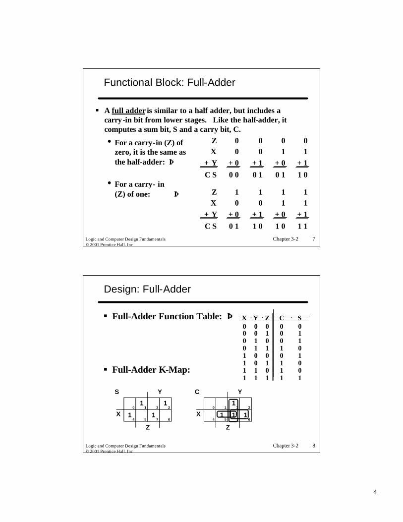
Functional Block: Full-Adder
§ A full adder is similar to a half adder, but includes a carry-in bit from lower stages. Like the half-adder, it computes a sum bit, S and a carry bit, C.
• For a carry-in (Z) of zero, it is the same as the half-adder: ⇒
• For a carry- in(Z) of one: ⇒
Z 0 0 0 0X 0 0 1 1
+ Y + 0 + 1 + 0 + 1C S 0 0 0 1 0 1 1 0
Z 1 1 1 1X 0 0 1 1
+ Y + 0 + 1 + 0 + 1C S 0 1 1 0 1 0 1 1
Logic and Computer Design Fundamentals© 2001 Prentice Hall, Inc
Chapter 3-2 8
Design: Full-Adder
§ Full-Adder Function Table: ⇒
§ Full-Adder K-Map:
X Y Z C S0 0 0 0 00 0 1 0 10 1 0 0 10 1 1 1 01 0 0 0 11 0 1 1 01 1 0 1 01 1 1 1 1
X
Y
Z
0 1 3 2
4 5 7 61
1
1
1
S
X
Y
Z
0 1 3 2
4 5 7 61 11
1
C

5
Logic and Computer Design Fundamentals© 2001 Prentice Hall, Inc
Chapter 3-2 9
Design: Full-Adder
§ From the K-Map, we get:
§ The S function is the three-bit XOR function (Odd Function):
§ The Carry bit C is 1 if both X and Y are 1 (the sum is 2), or if the sum is 1 and a carry-in (Z) occurs. Thus C can be re-written as:
§ The term X·Y is carry generate.
§ The term X⊕Y is carry propagate.
ZYZXYXCZYXZYXZYXZYXS
++=+++=
ZYXS ⊕⊕=
Z)YX(YXC ⊕+=
Logic and Computer Design Fundamentals© 2001 Prentice Hall, Inc
Chapter 3-2 10
Implementation: Full Adder
§ Full Adder Schematic ⇒
§ Here X, Y, and Z, and C (from the previous pages) are A, B, Ci and Co respectively. Also,
G = Generate and P = Propagate.
§ Note: This is really a combination of a 3-bit odd function (for S = sum) and Carry logic:
(G = Generate) OR (P =Propagate AND Ci = Carry In)
Co = G + P · Ci
A
BP
G
S
Co
Ci

6
Logic and Computer Design Fundamentals© 2001 Prentice Hall, Inc
Chapter 3-2 11
Parallel Binary Adders
§ To add more than one bit, we "bundle" sets of logical signals together and build devices that operate on the whole set in parallel.
§ Example: 4-bit binary adder:Adds an input vector "A(3..0) " to "B(3..0)“ to get a sum S(3..0) thus: ⇒
§ Note: the carry out of Stage i becomes the carry in of Stage i+1.
Description Subscript3 2 1 0
Name
Input Carry 0 1 1 0 Ci
Augend 1 0 1 1 Ai
Addend 0 0 1 1 Bi
Sum 1 1 1 0 S i
Output Carry
0 0 1 1 Ci+1
Logic and Computer Design Fundamentals© 2001 Prentice Hall, Inc
Chapter 3-2 12
4-bit Ripple-Carry Binary Adder
§ A four-bit Full Adder made from four 1-bit Full Adders: ⇒
§ Here FA is a Full-Adder from before: ⇒ A
BP
G
S
Co
Ci
Co Ci
x y
SFA
A(3)B(3)
S(3)
Co Ci
x y
SFA
B(2)
S(2)
Co Ci
x y
SFA
B(1)
S(1)
Co Ci
x y
SFA
S(0)
B(0)A(2) A(1) A(0)
C(4) C(3) C(2) C(1) C(0)
7
Logic and Computer Design Fundamentals© 2001 Prentice Hall, Inc
Chapter 3-2 13
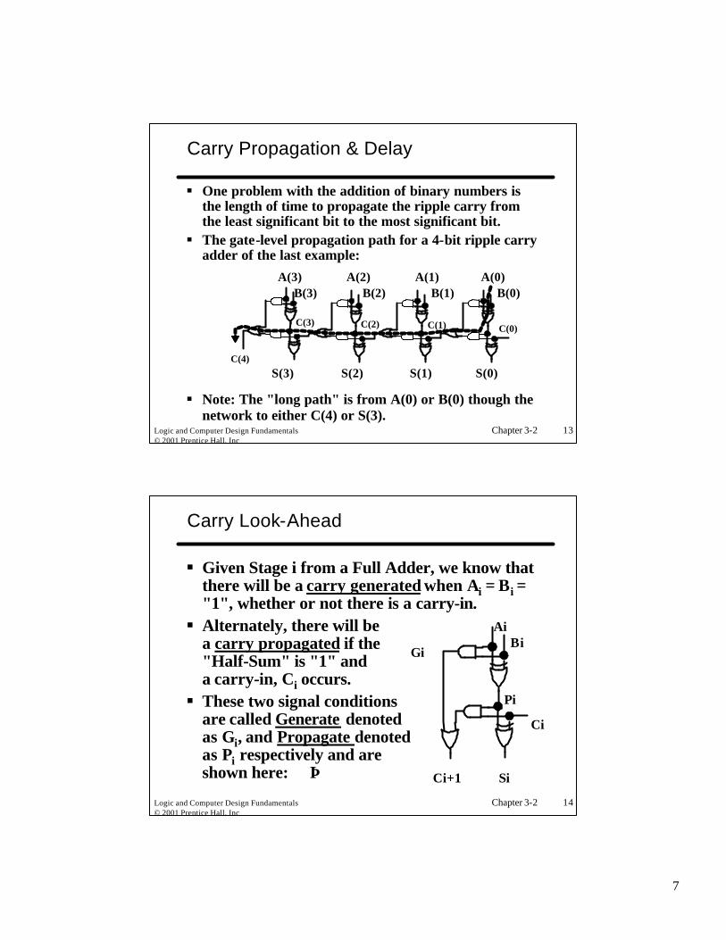
Carry Propagation & Delay
§ One problem with the addition of binary numbers is the length of time to propagate the ripple carry from the least significant bit to the most significant bit.
§ The gate-level propagation path for a 4-bit ripple carry adder of the last example:
§ Note: The "long path" is from A(0) or B(0) though the network to either C(4) or S(3).
A(3)B(3)
S(3)
B(2)
S(2)
B(1)
S(1) S(0)
B(0)A(2) A(1) A(0)
C(4)
C(3) C(2) C(1) C(0)
Logic and Computer Design Fundamentals© 2001 Prentice Hall, Inc
Chapter 3-2 14
Carry Look-Ahead
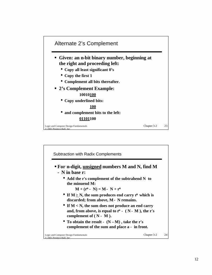
§ Given Stage i from a Full Adder, we know that there will be a carry generated when Ai = Bi = "1", whether or not there is a carry-in.§ Alternately, there will be
a carry propagated if the "Half-Sum" is "1" and a carry-in, Ci occurs. § These two signal conditions
are called Generate denoted as Gi, and Propagate denoted as Pi respectively and are shown here: ⇒
AiBi
Pi
Gi
SiCi+1
Ci

8
Logic and Computer Design Fundamentals© 2001 Prentice Hall, Inc
Chapter 3-2 15
Carry Look-Ahead (Continued)
§ By defining the equations for the Full Adder in term of the Pi and Gi, we have:
§ And the output sum S(i) and carry C(i+1) is defined as:
§ Starting the stage numbering at zero, we have:
where C0 is a carry in to the least significant bit.
iiiiii BAGBAP =⊕=
iii1iiii CPGCCPS +=⊕= +
001230123
1232334
CPPPPGPPP
GPPGPGC++
++=
Logic and Computer Design Fundamentals© 2001 Prentice Hall, Inc
Chapter 3-2 16
Carry Look-Ahead (Continued)
§ Look at the following addition examples, all of which generate a carry of 1 out of the third stage:
Use a carry into stage 0 and
1xxx+1xxx1xxxx
Generate a carry inStage3.
11xx+01xx10xxx
Generate a carry inStage 2 and propagate it through stage 3.
111x+001x100xx
Generate a carry inStage 1 and propagate it through stage 2 & stage 3.
1111+00011000x
Generate a carry in stage 0 and propagate it through Stage 1, stage 2, & stage 3.
1111+000010000
propagate it through stage 0, Stage 1, stage 2 & stage 3.

9
Logic and Computer Design Fundamentals© 2001 Prentice Hall, Inc
Chapter 3-2 17
Group Carry Look-Ahead Logic
§ Figure 3-28 in the text shows how to implement a carry look-ahead circuit for four bits. This could be extended to more than four bits. In practice, though, it becomes more difficult to implement this over more than a few bits. The concept can be extended another level by considering a Group Generate (G 0-3) and Group Propagate (P 0-3) logic condition:
§ Using these two equations:
§ Thus, it is possible to have four 4-bit adders use one of the same carry look-ahead circuits to add 16 bits!
012330
0012312323330
PPPPP
GPPPPGPPGPGG=
+++=
−
−
030304 CPGC −− +=
Logic and Computer Design Fundamentals© 2001 Prentice Hall, Inc
Chapter 3-2 18
Complements
§ Subtraction of numbers requires a different algorithm from that for addition§ Adding the complement of a number is
equivalent to subtraction§ We will discuss two complements:
• Diminished Radix Complement• Radix Complement
§ Subtraction will be done by adding the complement of the subtrahend

10
Logic and Computer Design Fundamentals© 2001 Prentice Hall, Inc
Chapter 3-2 19
Diminished Radix Complement
§ Given a number N in Base r having n digits, the (r – 1)’s-complement (called the Diminished Radix Complement) is defined as: (rn – 1) – N§ Example:
• For r = 10, N = 123410, n = 4 (4 digits),we have:
(rn – 1) = 10,000 – 1 = 999910• The 9's complement of 123410 is then:
999910 - 123410 = 876510
Logic and Computer Design Fundamentals© 2001 Prentice Hall, Inc
Chapter 3-2 20
Binary 1's Complement
§ For r = 2, N = 011100112, n = 8 (8 digits):(rn – 1) = 256 -1 = 25510 or 111111112
§ The 1's complement of 011100112 is then:11111111
– 0111001110001100
§ Since the 2n – 1 factor consists of all 1's and since 1 – 0 = 1 and 1 – 1 = 0, the one's complement is obtained by complementing each individual bit (bitwise NOT).

11
Logic and Computer Design Fundamentals© 2001 Prentice Hall, Inc
Chapter 3-2 21
Radix Complement
§ Given a number N in Base r having n digits, the r's complement (called the radix complement) is defined as:
• rn – N for N ≠ 0 and• 0 for N = 0
§ The radix complement is obtained by adding 1 to the diminished radix complement
§ Example:•For r = 10, N = 123410, n = 4 (4 digits), we have:
rn = 10,00010
•The 10's complement of 1234 is then10,000 - 1234 = 876610 or 8765 + 1 (9's complement
plus 1)
Logic and Computer Design Fundamentals© 2001 Prentice Hall, Inc
Chapter 3-2 22
Binary 2's Complement
§ For r = 2, N = 011100112, n = 8 (8 digits), we have:(rn ) = 25610 or 1000000002§ The 2's complement of 01110011 is then:
100000000– 01110011
10001101§ Note the result is the 1's complement plus
1
12
Logic and Computer Design Fundamentals© 2001 Prentice Hall, Inc
Chapter 3-2 23
Alternate 2’s Complement
§ Given: an n-bit binary number, beginning at the right and proceeding left: • Copy all least significant 0’s• Copy the first 1• Complement all bits thereafter.
§ 2’s Complement Example:10010100
• Copy underlined bits:100
• and complement bits to the left:01101100
Logic and Computer Design Fundamentals© 2001 Prentice Hall, Inc
Chapter 3-2 24
Subtraction with Radix Complements
§For n-digit, unsigned numbers M and N, find M − N in base r:
• Add the r's complement of the subtrahend N to the minuend M:
M + (rn − N) = M − N + rn
• If M > N, the sum produces end carry rn which is discarded; from above, M − N remains.
• If M < N, the sum does not produce an end carry and, from above, is equal to rn − ( N − M ), the r's complement of ( N − M ).
• To obtain the result − (N – M) , take the r's complement of the sum and place a − in front.

13
Logic and Computer Design Fundamentals© 2001 Prentice Hall, Inc
Chapter 3-2 25
Unsigned 10’s Complement Subtraction Example 1
§ Find 54310 – 12310
543 543– 123 + 877
420§ The carry of 1 indicates that no
correction of the result is required.
1
10’s comp
Logic and Computer Design Fundamentals© 2001 Prentice Hall, Inc
Chapter 3-2 26
Unsigned 10’s Complement Subtraction Example 2
§ Find 12310 – 54310
123 123– 543 + 457
580 520§ The carry of 0 indicates that a correction
of the result is required.§ Result = – (520)
010’s comp
10’s comp

14
Logic and Computer Design Fundamentals© 2001 Prentice Hall, Inc
Chapter 3-2 27
Unsigned 2’s Complement Subtraction Example 1
§ Find 010101002 – 010000112
01010100 01010100– 01000011 + 10111101
00010001§ The carry of 1 indicates that no
correction of the result is required.
12’s comp
Logic and Computer Design Fundamentals© 2001 Prentice Hall, Inc
Chapter 3-2 28
Unsigned 2’s Complement Subtraction Example 2
§ Find 010000112 – 010101002
01000011 01000011– 01010100 + 10101100
1110111100010001
§ The carry of 0 indicates that a correction of the result is required.§ Result = – (00010001)
02’s comp
2’s comp
15
Logic and Computer Design Fundamentals© 2001 Prentice Hall, Inc
Chapter 3-2 29
Subtraction with Diminished Radix Complement
§ For n-digit, unsigned numbers M and N, find M − N in base r:• Add the (r − 1)'s complement of the subtrahend N to the
minuend M:M + (rn − 1 − N) = M − N + rn − 1
• If M > N, the result is excess by rn − 1. The end carry rn when discarded removes rn, leaving a result short by 1. To fix this shortage, whenever and end carry occurs we all 1 in the LSB position. This is called end-around carry.
• If M < N, the sum does not produce an end carry and, from above, is equal to rn − 1 − ( N − M ), the r − 1 's complement of ( N − M ).
• To obtain the result − (N – M) , take the r − 1 's complement of the sum and place a − in front.
Logic and Computer Design Fundamentals© 2001 Prentice Hall, Inc
Chapter 3-2 30
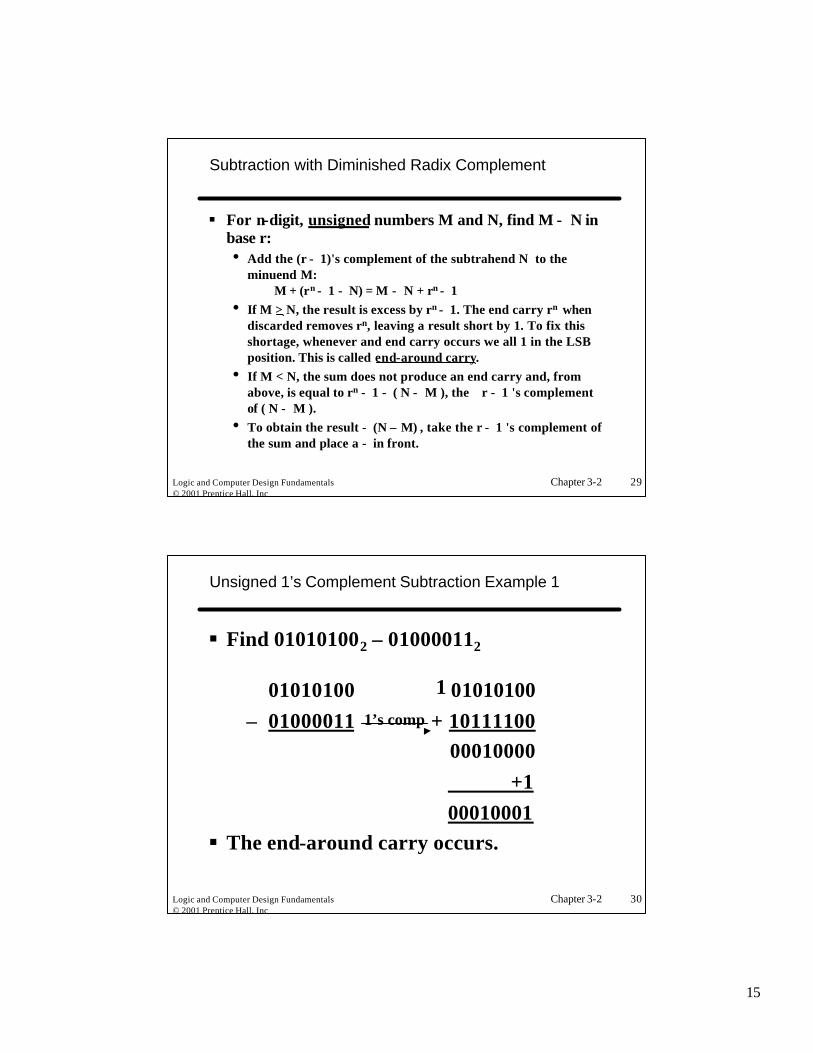
Unsigned 1’s Complement Subtraction Example 1
§ Find 010101002 – 010000112
01010100 01010100– 01000011 + 10111100
00010000+1
00010001§ The end-around carry occurs.
11’s comp

16
Logic and Computer Design Fundamentals© 2001 Prentice Hall, Inc
Chapter 3-2 31
Unsigned 1’s Complement Subtraction Example 2
§ Find 010000112 – 010101002
01000011 01000011– 01010100 + 10101011
1110111000010001
§ The carry of 0 indicates that a correction of the result is required.§ Result = – (00010001)
1’s comp
1’s comp
0
Logic and Computer Design Fundamentals© 2001 Prentice Hall, Inc
Chapter 3-2 32
Signed Integers
§Positive numbers and zero can be represented by unsigned n-digit, radix r numbers. We need a representation for negative numbers . §To represent a sign (+ or–) we need exactly one more bit of information (1 binary digit gives 21 = 2 elements which is exactly what is needed).§Since computers use binary numbers, by convention, (and, for convenience), the most significant bit is interpreted as a sign bit:
s an–2 … a2a1a0where:
s = 0 for Positive numbers s = 1 for Negative numbers
and ai = 0 or 1 represent in some form the magnitude.

17
Logic and Computer Design Fundamentals© 2001 Prentice Hall, Inc
Chapter 3-2 33
Signed Integer Representations
§Signed-Magnitude – here the n – 1 digits are interpreted as a positive magnitude.§Signed-Complement – here the digits are interpreted as the rest of the complement of the number. There are two possibilities here:§Signed One's Complement –
• Uses 1's Complement Arithmetic
§Signed Two's Complement –• Use 2's Complement Arithmetic
Logic and Computer Design Fundamentals© 2001 Prentice Hall, Inc
Chapter 3-2 34
Signed Integer Representation Example
§ r =2, n=3
Number Sign -Mag. 1's Comp. 2's Comp.+3 011 011 011+2 010 010 010+1 001 001 001+0 000 000 000– 0 100 111 —– 1 101 110 111– 2 110 101 110– 3 111 100 101– 4 — — 100
18
Logic and Computer Design Fundamentals© 2001 Prentice Hall, Inc
Chapter 3-2 35
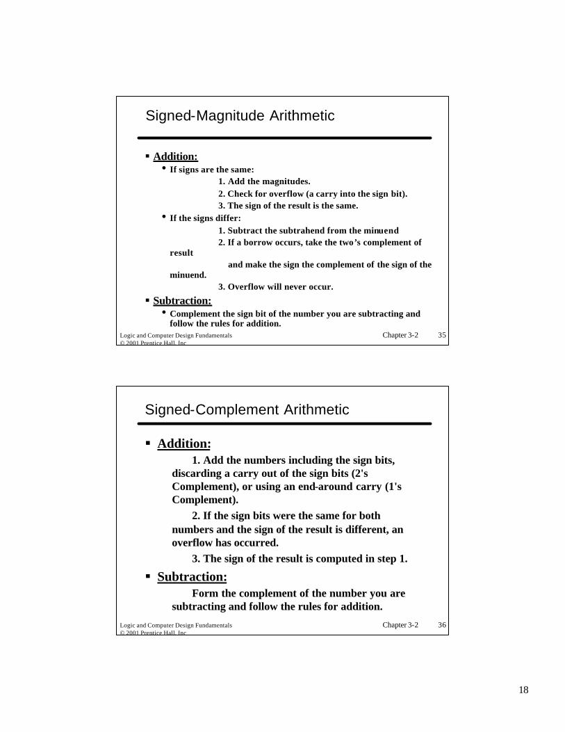
Signed-Magnitude Arithmetic
§ Addition:• If signs are the same:
1. Add the magnitudes.2. Check for overflow (a carry into the sign bit).3. The sign of the result is the same.
• If the signs differ:1. Subtract the subtrahend from the minuend2. If a borrow occurs, take the two’s complement of
resultand make the sign the complement of the sign of the
minuend.3. Overflow will never occur.
§ Subtraction:• Complement the sign bit of the number you are subtracting and
follow the rules for addition.
Logic and Computer Design Fundamentals© 2001 Prentice Hall, Inc
Chapter 3-2 36
Signed-Complement Arithmetic
§ Addition:1. Add the numbers including the sign bits,
discarding a carry out of the sign bits (2's Complement), or using an end-around carry (1's Complement).
2. If the sign bits were the same for both numbers and the sign of the result is different, an overflow has occurred.
3. The sign of the result is computed in step 1.
§ Subtraction:Form the complement of the number you are
subtracting and follow the rules for addition.

19
Logic and Computer Design Fundamentals© 2001 Prentice Hall, Inc
Chapter 3-2 37
Examples
§ Signed-magnitude arithmetic§ Signed 2’s complement arithmetic§ Signed 1’s complement arithmetic
Logic and Computer Design Fundamentals© 2001 Prentice Hall, Inc
Chapter 3-2 38
2’s Complement Adder/Subtractor
§ Subtraction can be accomplished by addition of the Two's Complement.
1. Complement each bit (One's Comp.)2. Add one to the result.
§ The following circuit computes A - B:§ When the Carry-In
is 1, the 2’s comp of B is formed using XORs to form the 1’s comp and adding the 1 on C(0). Co Ci
x y
S
FA
A(3)B(3)
S(3)
Co Ci
x y
S
FA
B(2)
S(2)
Co Ci
x y
S
FA
B(1)
S(1)
Co Ci
x y
S
FA
S(0)
B(0)A(2) A(1) A(0)
C(4) C(3) C(2) C(1)
C(0)

20
Logic and Computer Design Fundamentals© 2001 Prentice Hall, Inc
Chapter 3-2 39
Overflow Detection and comments
§ Overflow detection example§ Comments on hardware for
• Sign-Magnitude• Complement-Based• Overflow detection hardware
Logic and Computer Design Fundamentals© 2001 Prentice Hall, Inc
Chapter 3-2 40
Binary Multiplication
§The binary digit multiplication table is trivial:
§This is simply the Boolean AND function.§Form larger products the same way we
form larger products in base 10.
(a × b) b = 0 b =1
a = 0 0 0
a = 1 0 1

21
Logic and Computer Design Fundamentals© 2001 Prentice Hall, Inc
Chapter 3-2 41
Review of Decimal Multiplication
§ Perform base 10 multiplication by:• Computing partial products, and• Justifying and summing the partial
products.§ To compute partial products:
• Multiply the row of multiplicand digits by each multiplier digit, one at a time.
§ Partial product formation here require carries to be added – more complex than binary
Logic and Computer Design Fundamentals© 2001 Prentice Hall, Inc
Chapter 3-2 42
Example: (237 x 149) Base 10
§ Partial products are: 237 × 9, 237 × 4, and 237 × 1§ Note that the partial product
summation for n digit, base 10 numbers requires adding up to n digits (with carries).§ Note also n x m digit
multiply generates up to an m+n digit result.
2 3 7
× 1 4 9
2 1 3 3
9 4 8 -
+ 2 3 7 - -
3 5 3 1 3

22
Logic and Computer Design Fundamentals© 2001 Prentice Hall, Inc
Chapter 3-2 43
Binary Multiplication Algorithm
§ We compute base 2 multiplication by:• Computing partial products, and• Justifying and summing the partial products. (same as
decimal!)§ To compute partial products:
• Multiply the row of multiplicand digits by each multiplier digit, one at a time.
• With binary numbers, partial products are very simple! They are either:§ all zero (if the multiplier digit is zero), or§ the same as the multiplicand (if the multiplier digit is one).
§ Note: No carries are added in partial product formation!
Logic and Computer Design Fundamentals© 2001 Prentice Hall, Inc
Chapter 3-2 44
Example: (101 x 011) Base 2
§ Partial products are: 101 x 0, 101 x 1, and 101 x 1§ Note that the partial product
summation for n digit, base 2 numbers requires adding up to n digits (with carries) in a column.§ Note also n x m digit
multiply generates up to an m + n digit result (same as decimal).
1 0 1
× 0 1 1
1 0 1
1 0 1
0 0 0
0 0 1 1 1 1

23
Logic and Computer Design Fundamentals© 2001 Prentice Hall, Inc
Chapter 3-2 45
Multiplier Boolean Equations
§ We can also make an n x m "block" multiplier and use that to form partial products.§ Example: 2 x 2 – The logic equations for each
partial-product binary digit are shown below:§ We need to "add" the columns
to get the product bits P0, P1, P2, and P3.§ Note that some
columns may generate carries.
b1 b0X a1 a0
(a0 ⋅ b1) (a0 ⋅ b0)+ (a1 ⋅ b1) (a1 ⋅ b0)P3 P2 P1 P0
Logic and Computer Design Fundamentals© 2001 Prentice Hall, Inc
Chapter 3-2 46
Multiplier Arrays Using Adders
§ An implementation of the 2 x 2 multiplier array is shown (Figure 3-33):
A B
Co SHA
a0
a1
b0b1
A B
Co SHA
P0P1P2P3

24
Logic and Computer Design Fundamentals© 2001 Prentice Hall, Inc
Chapter 3-2 47
Multiplier Using Wide Adders
§ A more "structured" way to develop an n × m multiplier is to sum partial products using adder trees§ The partial products are formed using an n × m
array of AND gates§ Partial products are summed using m – 1 adders
of width n bits§ Example: 4-bit by 3-bit adder§ Text Figure 3-34 shows a 4 × 3 = 12 element
array of AND gates and 2 4-bit adders
Logic and Computer Design Fundamentals© 2001 Prentice Hall, Inc
Chapter 3-2 48
Cellular Multiplier Arrays
§ Another way to imple-ment multipliers is to use an n × m cellular array structure of uniform elements as shown:§ Each element computes
a single bit product equal to ai·bj, and implements a single bit full adder
Carry [ j, (k - 1)]
a[ j ]
b[ k ]
pp [ j , k ]
Cell [ j , k ]
Column Sum from above
Carry [ j , k ]
Column Sum to below
A BCo
SFACi
25
Logic and Computer Design Fundamentals© 2001 Prentice Hall, Inc
Chapter 3-2 49
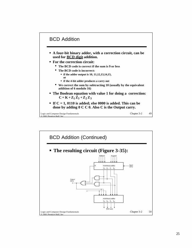
BCD Addition
§ A four-bit binary adder, with a correction circuit, can be used for BCD digit addition.§ For the correction circuit:
• The BCD code is correct if the sum is 9 or less• The BCD code is incorrect:§ if the adder output is 10, 11,12,13,14,15,
or§ if the 4-bit adder produces a carry out
• We correct the sum by subtracting 10 (usually by the equivalent addition of 6 modulo 16)
§ The Boolean equation with value 1 for doing a correction:
§ If C = 1, 0110 is added; else 0000 is added. This can be done by adding 0 C C 0. Also C is the Output carry.
3231 ZZZZKC ++=
Logic and Computer Design Fundamentals© 2001 Prentice Hall, Inc
Chapter 3-2 50
BCD Addition (Continued)
§ The resulting circuit (Figure 3-35):

26
Logic and Computer Design Fundamentals© 2001 Prentice Hall, Inc
Chapter 3-2 51
Overview of Verilog – Part 1
§ Objectives§ Verilog Basics
• Notation• Keywords & Constructs• Operators
§ Types of Descriptions• Structural• Dataflow§ Boolean Equations§ Conditions using Binary Combinations§ Conditions using Binary Decisions
• Behavioral & Hierarchical• Process (Procedural) – not discussed
Logic and Computer Design Fundamentals© 2001 Prentice Hall, Inc
Chapter 3-2 52
Objectives
§ To become familiar with the hardware description language (HDL) approach to specifying designs• Be able to read a simple Verilog HDL
description• Be able to write a simple Verilog HDL
description using a limited set of syntax and semantics
• Understanding the need for a “hardware view” when reading and writing an HDL

27
Logic and Computer Design Fundamentals© 2001 Prentice Hall, Inc
Chapter 3-2 53
Verilog Notation - 1
§ Verilog is: • Case sensitive• Based on the programming language C
§ Comments• Single Line
// [end of line]
• Multiple Line/*
*/
§ List element separator: ,§ Statement terminator: ;
Logic and Computer Design Fundamentals© 2001 Prentice Hall, Inc
Chapter 3-2 54
Verilog Notation - 2
§ Binary Values for Constants and Variables• 0• 1
• X,x – Unknown• Z,z – High impedance state (open circuit)
§ Constants• n’b[integer]: 1’b1 = 1, 8’b1 = 000000001, 4’b0101=
0101, 8’bxxxxxxxx, 8’bxxxx = 0000xxxx• n’h[integer]: 8’hA9 = 10101001, 16’hf1=
0000000011110001
§ Identifier Examples• Scalar: A,C,RUN,stop,m,n• Vector: sel[0:2], f[0:5], ACC[31:0], SUM[15:0],
sum[15:0]

28
Logic and Computer Design Fundamentals© 2001 Prentice Hall, Inc
Chapter 3-2 55
Verilog Keywords & Constructs - 1
§ Keywords are lower case§ module – fundamental building block for Verilog
designs • Used to construct design hierarchy• Cannot be nested
§ endmodule – ends a module – not a statement=> no “;”
§ Module Declaration • module module_name (module_port, module_port, …);• Example: module full_adder (A, B, c_in,
c_out, S);
Logic and Computer Design Fundamentals© 2001 Prentice Hall, Inc
Chapter 3-2 56
Verilog Keywords & Constructs - 2
§ Input Declaration• Scalar § input list of input identifiers;§ Example: input A, B, c_in;
• Vector§ input[range] list of input identifiers;§ Example: input[15:0] A, B, data;
§ Output Declaration• Scalar Example: output c_out, OV, MINUS;• Vector Example: output[7:0] ACC, REG_IN,
data_out;

29
Logic and Computer Design Fundamentals© 2001 Prentice Hall, Inc
Chapter 3-2 57
Verilog Keywords & Constructs - 3
§ Primitive Gates• buf, not, and, or, nand, nor, xor, xnor• Syntax: gate_operator instance_identifier
(output, input_1, input_2, …)• Examples:
and A1 (F, A, B); //F = A Bor O1 (w, a, b, c)
O2 (x, b, c, d, e); //w=a+b+c,x=b+c+d+e
Logic and Computer Design Fundamentals© 2001 Prentice Hall, Inc
Chapter 3-2 58
Verilog Operators - 1
§ Bitwise Operators~ NOT& AND| OR^ XOR^~ or ~^ XNOR
§ Example: input[3:0] A, B;output[3:0] Z ;
assign Z = A | ~B;
30
Logic and Computer Design Fundamentals© 2001 Prentice Hall, Inc
Chapter 3-2 59
Verilog Operators - 2
§ Arithmetic Operators+, -, (plus others)
§ Logical & Relational Operators!, &&, | |, = =, !=, >=, <=, >, < (plus others)
§ Concatenation & Replication Operators{identifier_1, identifier_2, …}{n{identifier}}• Examples: {REG_IN[6:0],Serial_in},{8 {1’b0}}
Logic and Computer Design Fundamentals© 2001 Prentice Hall, Inc
Chapter 3-2 60
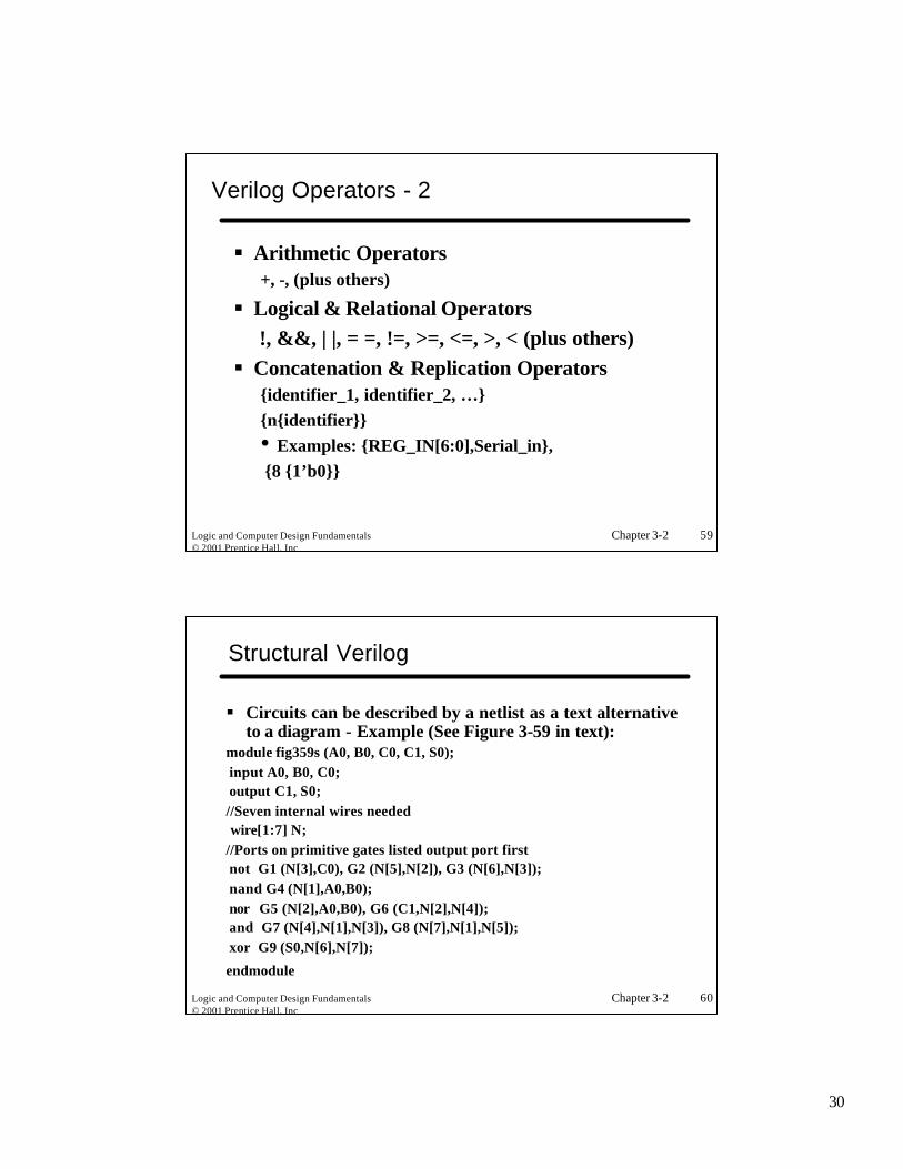
Structural Verilog
§ Circuits can be described by a netlist as a text alternative to a diagram - Example (See Figure 3-59 in text):
module fig359s (A0, B0, C0, C1, S0);input A0, B0, C0;output C1, S0;//Seven internal wires neededwire[1:7] N;
//Ports on primitive gates listed output port firstnot G1 (N[3],C0), G2 (N[5],N[2]), G3 (N[6],N[3]);nand G4 (N[1],A0,B0);nor G5 (N[2],A0,B0), G6 (C1,N[2],N[4]);and G7 (N[4],N[1],N[3]), G8 (N[7],N[1],N[5]);xor G9 (S0,N[6],N[7]);
endmodule

31
Logic and Computer Design Fundamentals© 2001 Prentice Hall, Inc
Chapter 3-2 61
Dataflow Verilog - 1
§ Circuit function can be described by assign statements using Boolean equations (See Figure 3-59 in text):
module fig359d (A0, B0, C0, C1, S0);input A0, B0, C0;output C1, S0;wire[1:2] N;assign N[1] = ~(A0 & B0); /*Note: Cannot write ~& for
NAND */assign N[2] = ~(A0 | B0);assign C1 = ~((N[1] & ~C0) | N[2]);assign S0 = (~N[2] & N[1])^(~(~C0));endmodule
Logic and Computer Design Fundamentals© 2001 Prentice Hall, Inc
Chapter 3-2 62
Dataflow Verilog - 2
§ Circuit function can be described by assign statements using the conditional operator with binary combinations as in a truth table (See Figure 3-14 in text):
module fig314dm (A, E_n, D_n);input[1:0] A;input E_n;output[3:0] D_n;//Conditional: (X) ? Y: Z - if X is true, then Y,else Zassign D_n = {4{E_n}}&(
(A == 2'b00) ? 4'b1110:(A == 2'b01) ? 4'b1101:(A == 2'b10) ? 4'b1011:(A == 2'b11) ? 4'b0111:4'bxxxx);
endmodule

32
Logic and Computer Design Fundamentals© 2001 Prentice Hall, Inc
Chapter 3-2 63
Dataflow Verilog - 3
§ Circuit function can be described by assign statements using the conditional operator for binary decisions on inputs(See Figure 3-14 in text):
module fig314dc (A, E_n, D_n);input[1:0] A;input E_n;output[3:0] D_n;/* Conditional: (X) ? Y: Z - if X is true, then Y,else Z */assign D_n = {4{E_n}} & (A[1] ? (A[0] ? 4'h7 : 4'hB): (A[0] ?
4'hD : 4'hE));endmodule
Logic and Computer Design Fundamentals© 2001 Prentice Hall, Inc
Chapter 3-2 64
Behavioral & Hierarchical Verilog
§ Circuit function can be described by assign statements at higher than the logic level (See Figure 3-31 in text):
module addsub (A, B, R, sub) ;input [3:0] A, B ;output [3:0] R ;//See Fig. 3-51 for carry outinput sub ;wire [3:0] data_out;add A1 (A, data_out, sub, R);M1comp C1 (B, data_out, sub);endmodule

33
Logic and Computer Design Fundamentals© 2001 Prentice Hall, Inc
Chapter 3-2 65
Behavioral & Hierarchical Verilog
module add (X, Y, C_in, S);input [3:0] X, Y;input C_in;output [3:0] S;assign S = X + Y + {3'b0, C_in};endmodulemodule M1comp (data_in, data_out, comp);input[3:0] data_in;input comp;output [3:0] data_out;assign data_out = {4{comp}} ^ data_in;endmodule
Logic and Computer Design Fundamentals© 2001 Prentice Hall, Inc
Chapter 3-2 66
Summary
§ Analysis• Forward – backward trace through the circuit to
obtain output equations or truth table• Vice versa will also find the equations and truth
table§ Know the functions performed by the following
functional blocks:• Decoders, Demultiplexers , Encoders, Multiplexers
§ Know how to implement Boolean functions using:• Multiplexers • Decoders