Embed Size (px)
Citation preview
46
CHAPTER 3
COMBINED MULTIPULSE MULTILEVEL
INVERTER BASED STATCOM
3.1 INTRODUCTION
Static synchronous compensator is a shunt connected reactive power
compensation device that is capable of generating or absorbing reactive power. The
output voltage of the STATCOM is adjusted to control power factor, regulate
voltage, stabilize power flow and improve the dynamic performance of the power
system. The voltage source inverter is an important part in the STATCOM that
generate a fundamental output voltage waveform with demanded magnitude and
phase angle in synchronism with the sinusoidal system which forces the reactive
power exchange required for compensation.
The traditional two-level VSI produces a square wave output as it switches the direct voltage source on and off. However for high voltage applications, a near sinusoidal ac voltage with minimal harmonic distortion is required. Several high power inverter topologies such as multipulse and multilevel inverters have been proposed for the implementation of FACTS devices.
The key problem with the multipulse inverter is the requirement of magnetic interfaces constituted by complex zig-zag phase shifting transformers which tremendously increases the cost of the complete system [57, 61]. However the multipulse inverter doesn’t have complex control and provides lesser THD. MLI is cheaper than MPI, but requires complex control circuit [57, 96] and produces more THD than MPI. Hence in order to obtain an optimal inverter topology, a trade off between the cost and complexity in control is necessary. Therefore a hybrid topology, involving both multipulse and multilevel inverter configurations extracting the advantages of them will be attractive.
47
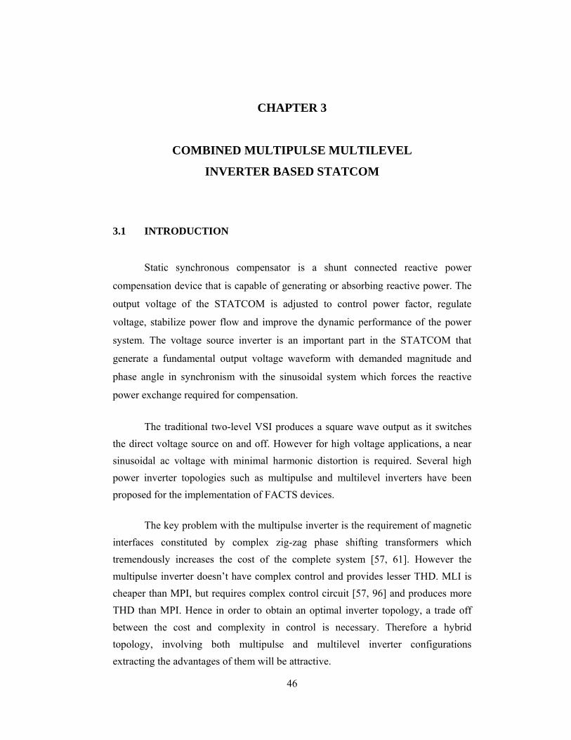
3.2 EXISTING 48-PULSE INVERTER TOPOLOGY
In multi-pulse operation, the harmonic content can be significantly reduced
by using several pulses in each half cycle of the output voltage. The 48-pulse
inverter has low harmonic rate on the ac side and can be used for high power
FACTS controllers without ac filters. The 48-pulse inverter is realized by combining
eight 6-pulse voltage source inverters with adequate phase shifts between them. The
configuration of 48-pulse inverter is depicted in the Fig. 3.1 where each of the VSI
output is connected to the phase shifting transformer. Four of them are connected to
a Y-Y transformer and the remaining four to a Δ-Y transformer. The output of the
phase shifting transformers is connected in series to cancel out the lower order
harmonics.
Fig. 3.1 48-pulse voltage source inverter
48
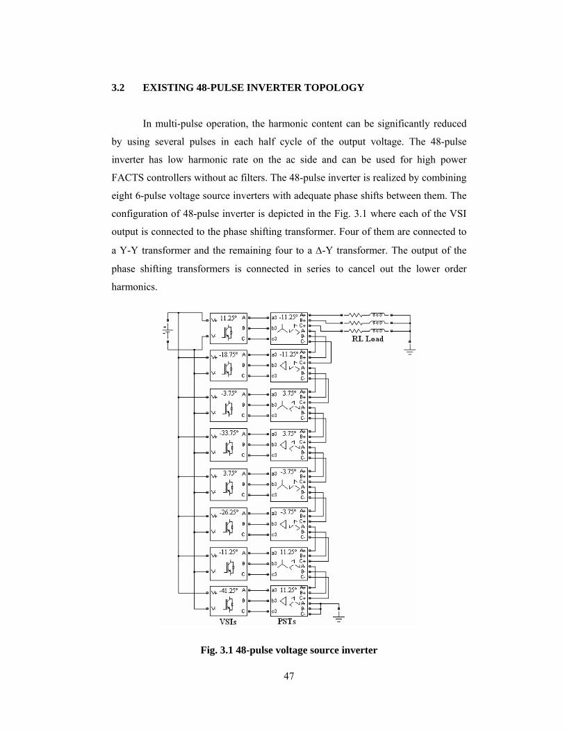
To create a 48-pulse waveform with a harmonic content in the order of
m = 48r±1, (where r = 0, 1, 2,...) the eight 6- pulse inverter voltages need to be phase
shifted. This is implemented by introducing appropriate phase shift in the phase
shifting transformer and the gate pulse pattern of individual VSI. Table 3.1 shows
the phase displacements applied to the gate pulse pattern of each VSI and the
corresponding phase shifting transformer. Thus a premium quality sinusoidal
voltage is obtained with the 48-pulse inverter configuration as depicted in Fig.3.2.
Table 3.1 Phase displacement for a 48-pulse VSI
Coupling transformer
Gate pulse pattern
Phase shifting transformer
Y-Y +11.25˚ -11.25˚
Δ-Y -18.75˚ -11.25˚
Y-Y -3.75 ˚ +3.75˚
Δ-Y -33.75˚ +3.75˚
Y-Y +3.75˚ -3.75˚
Δ-Y -26.25˚ -3.75˚
Y-Y -11.25˚ +11.25˚
Δ-Y -41.25˚ +11.25˚
Fig. 3.2 48-Pulse inverter output voltage
49
It is proposed to build up a forty eight pulse inverter topology through the
twenty four pulse configuration in which each individual two level inverters are
converted to 3-level diode clamped structures. This new topology enjoys the benefits
of both the MPI and MLI configurations and is referred as combined multipulse-
multilevel inverter topology. The harmonic performance of this inverter topology is
evaluated through MATLAB based simulation. It establishes that this structure
almost offers the same response as that of a forty eight pulse inverter in respect of
THD. Further the static synchronous compensator operation is realized using the
proposed high performance, reliable, flexible and cost effective inverter topology.
A closed loop controller based on decoupled control strategy is developed for
effectively operating the STATCOM over a wide range of power system operating
conditions.
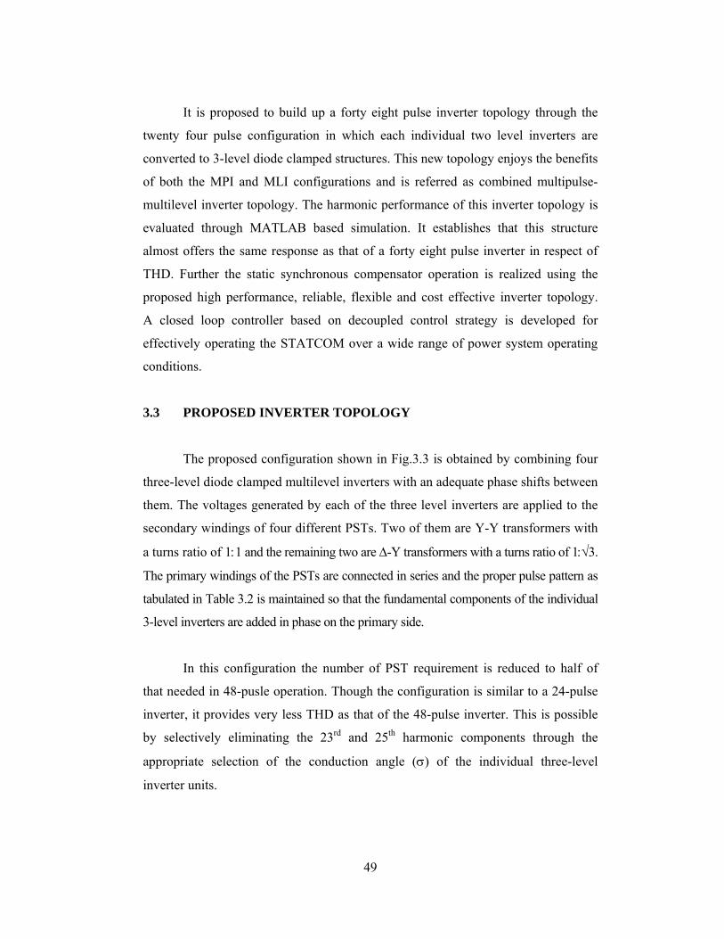
3.3 PROPOSED INVERTER TOPOLOGY
The proposed configuration shown in Fig.3.3 is obtained by combining four
three-level diode clamped multilevel inverters with an adequate phase shifts between
them. The voltages generated by each of the three level inverters are applied to the
secondary windings of four different PSTs. Two of them are Y-Y transformers with
a turns ratio of 1:1 and the remaining two are Δ-Y transformers with a turns ratio of 1:√3.
The primary windings of the PSTs are connected in series and the proper pulse pattern as
tabulated in Table 3.2 is maintained so that the fundamental components of the individual
3-level inverters are added in phase on the primary side.
In this configuration the number of PST requirement is reduced to half of
that needed in 48-pusle operation. Though the configuration is similar to a 24-pulse
inverter, it provides very less THD as that of the 48-pulse inverter. This is possible
by selectively eliminating the 23rd and 25th harmonic components through the
appropriate selection of the conduction angle (σ) of the individual three-level
inverter units.
50
Fig. 3.3 Combined multipulse-multilevel inverter
Table 3.2 Phase displacement for the combined multipulse-multilevel inverter
Coupling transformer
Gate pulse pattern
Phase shifting transformer
Y-Y +7.5˚ -7.5˚ Δ-Y -22.5˚ -7.5˚ Y-Y -7.5˚ +7.5˚ Δ-Y -37.5˚ +7.5˚
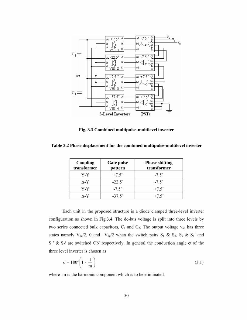
Each unit in the proposed structure is a diode clamped three-level inverter
configuration as shown in Fig.3.4. The dc-bus voltage is split into three levels by
two series connected bulk capacitors, C1 and C2. The output voltage van has three
states namely Vdc/2, 0 and –Vdc/2 when the switch pairs S1 & S2, S2 & S1′ and
S1′ & S2′ are switched ON respectively. In general the conduction angle σ of the
three level inverter is chosen as
1σ = 180° 1 - m
⎛ ⎞⎜ ⎟⎝ ⎠
(3.1)
where m is the harmonic component which is to be eliminated.
51
Fig. 3.4 Diode clamped 3-level inverter
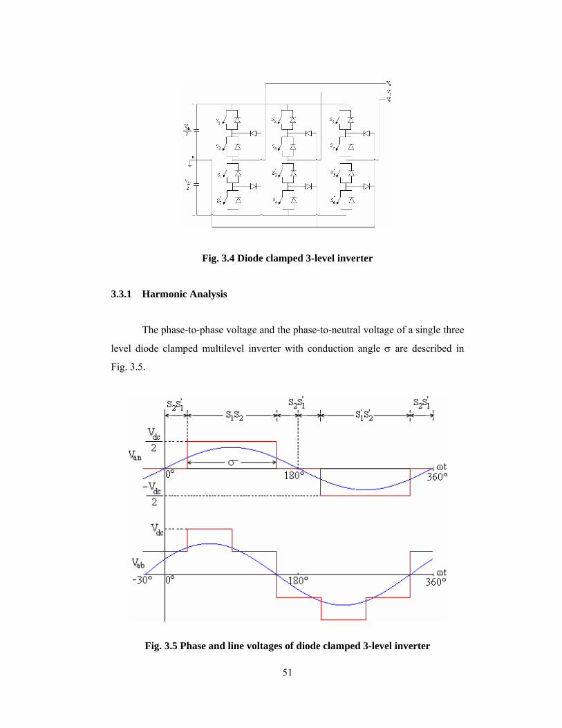
3.3.1 Harmonic Analysis
The phase-to-phase voltage and the phase-to-neutral voltage of a single three
level diode clamped multilevel inverter with conduction angle σ are described in
Fig. 3.5.
Fig. 3.5 Phase and line voltages of diode clamped 3-level inverter
52
Carrying out the Fourier analysis of the inverter output voltage, the
instantaneous phase-to-neutral voltage is expressed as:
( )man anv t = V sin mωt
m=1
∞∑ (3.2)
where m
DCan
2VV =
mπ
π - σcos m2
⎛ ⎞⎜ ⎟⎝ ⎠
(3.3)
Similarly the instantaneous phase-to-phase voltage is expressed as
( )ab abm
πv t = V sin mωt + m6m=1
∞ ⎛ ⎞∑ ⎜ ⎟
⎝ ⎠ (3.4)
where DCab m
4 V mσ mπV = sin cosmπ 2 6
(3.5)
The voltages vbc(t) and vca(t) exhibit a similar pattern except that they are
phase shifted by 120° and 240° respectively. Similarly the phase voltages vbn(t) and
vcn(t) are also phase shifted by 120° and 240° respectively. It contains only odd
harmonics in the order of 6r±1, where r is a numeral can assume values 1, 2, 3,…..
In general star and delta connected windings have a relative phase shift of
30° and the three-level inverters connected to each of these Y and Δ transformers
will give an overall 12-pulse operation and offers a better harmonic performance.
The output voltage will have a twelve pulse waveform, with harmonics of the order
of 12r±1. Thus the twelve pulse inverter will have 11th, 13th, 23rd, 25th,…..
harmonics with amplitudes of 1/11th, 1/13th, 1/23rd, 1/25th,…… respectively of the
fundamental ac voltage.
The relationship between the phase-to-phase voltage and the phase-to-neutral
voltage is expressed as:
( )mm
rab anv = -1 3 v (3.6)
For obtaining 12-pulse inverter the VSI1 output is connected to a Y-Y
transformer with a 1:1 turn ratio, and the line to neutral voltage using equation (3.6)
can be expressed as:

53
( )( )
abman r1
V1v t = sin mωt3 m=1 -1
∞∑ (3.7)
m = 6r ±1, r = 0,1,2,.....∀
If the VSI2 produces phase-to-phase voltages lagging by 30° with respect to
VSI1 and with the same magnitude, it is given by
( )2 mab abv t = V sin mωt
m=1
∞∑ (3.8)
If this inverter output is connected to a Δ-Y transformer with a 1:1/√3 turn
ratio, the line-to-neutral voltage in the Y-connected secondary will be
( )manY an2
v t = V sin mωtm=1
∞∑ (3.9)
Therefore line-to-line voltage in the secondary side is
( )mabY an2
mπv t = 3V sin mωt +6m=1
∞ ⎛ ⎞∑ ⎜ ⎟
⎝ ⎠ (3.10)
The 12-pulse inverter output is obtained by adding the equations (3.4)
and (3.10).
( ) ( ) ( )ab ab abY12 2v t = v t + v t (3.11)
( )12mab ab12
mπv t = V sin mωt +6m=1
∞ ⎛ ⎞∑ ⎜ ⎟
⎝ ⎠ (3.12)
m = 12r ±1, r = 0,1,2,......∀
since 12m m m mab ab an ab V = V + 3V = 2V
∴ ( )mab ab12
mπv t = 2 V sin mωt +6m=1
∞ ⎛ ⎞∑ ⎜ ⎟
⎝ ⎠ (3.13)
Similarly two twelve pulse inverters phase shifted by 15° from each other
can provide a 24-pulse inverter, with much lower harmonics in the ac side. The ac
output voltage will have 24r±1 order harmonics, i.e., 23rd, 25th, 47th, 49th,…..
54
harmonics, with magnitudes of 1/23rd, 1/25th, 1/47th, 1/49th,…. respectively, of the
fundamental ac voltage. Thus the output voltage of twenty four pulse inverter is
obtained as:
( ) ( )24 m
° °ab abv t = 4 V sin mωt + 22.5 m + 7.5 x
m=1
∞∑ (3.14)
( ) ( )24 m
° °an ab
4v t = V sin mωt + 22.5 m - 22.5 x3 m=1
∞∑ (3.15)
where x = 1 for positive sequence harmonics
x = -1 for negative sequence harmonics
m = 24r ±1, r = 0,1,2,......∀
In order to eliminate the 23rd and 25th harmonic components, the conduction
angle of the inverter is set to σ = 172.5° by choosing m = 24 in equation (3.1). This
configuration produces almost a near sinusoidal output voltage since the lowest
significant harmonic component is the 47th harmonic.
3.3.2 Harmonic Neutralisation
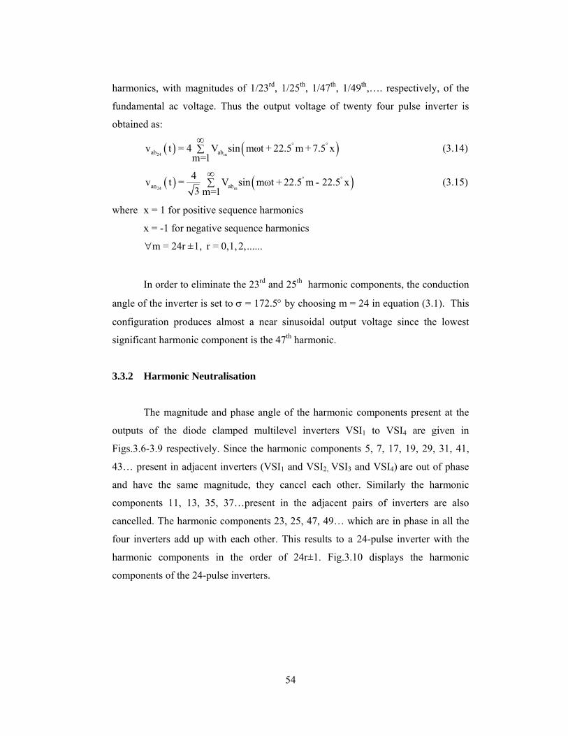
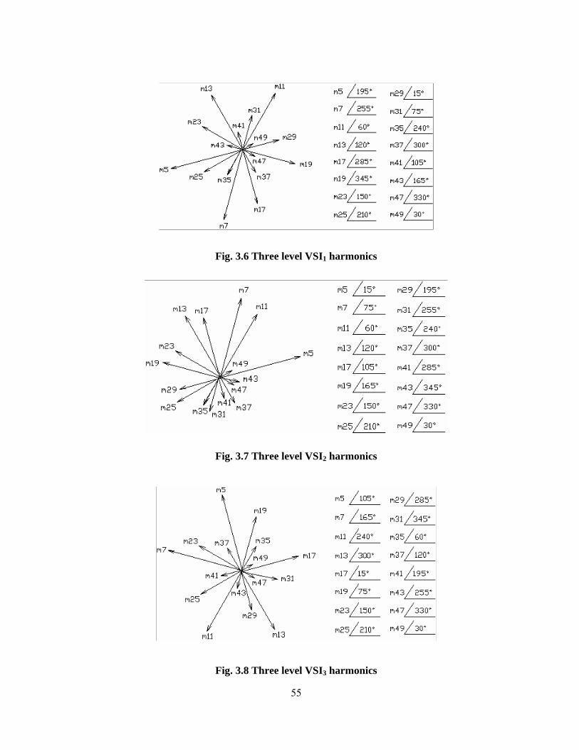
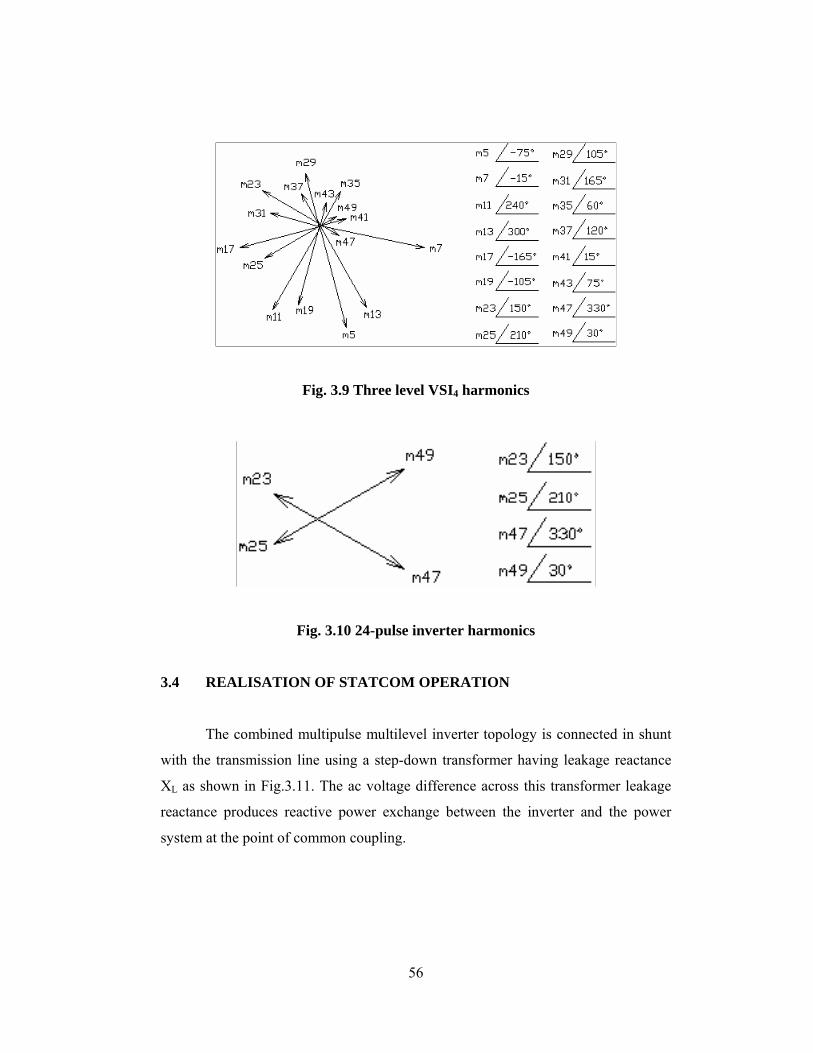
The magnitude and phase angle of the harmonic components present at the
outputs of the diode clamped multilevel inverters VSI1 to VSI4 are given in
Figs.3.6-3.9 respectively. Since the harmonic components 5, 7, 17, 19, 29, 31, 41,
43… present in adjacent inverters (VSI1 and VSI2, VSI3 and VSI4) are out of phase
and have the same magnitude, they cancel each other. Similarly the harmonic
components 11, 13, 35, 37…present in the adjacent pairs of inverters are also
cancelled. The harmonic components 23, 25, 47, 49… which are in phase in all the
four inverters add up with each other. This results to a 24-pulse inverter with the
harmonic components in the order of 24r±1. Fig.3.10 displays the harmonic
components of the 24-pulse inverters.
55
Fig. 3.6 Three level VSI1 harmonics
Fig. 3.7 Three level VSI2 harmonics
Fig. 3.8 Three level VSI3 harmonics
56
Fig. 3.9 Three level VSI4 harmonics
Fig. 3.10 24-pulse inverter harmonics
3.4 REALISATION OF STATCOM OPERATION
The combined multipulse multilevel inverter topology is connected in shunt
with the transmission line using a step-down transformer having leakage reactance
XL as shown in Fig.3.11. The ac voltage difference across this transformer leakage
reactance produces reactive power exchange between the inverter and the power
system at the point of common coupling.
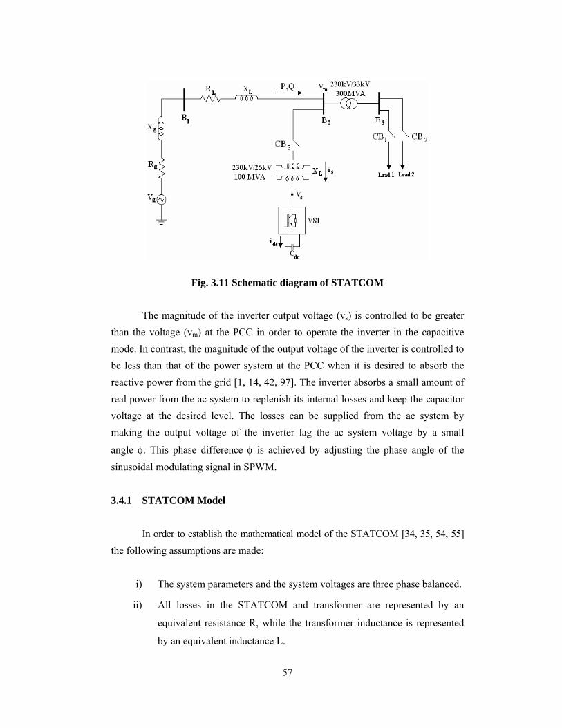
57
Fig. 3.11 Schematic diagram of STATCOM
The magnitude of the inverter output voltage (vs) is controlled to be greater than the voltage (vm) at the PCC in order to operate the inverter in the capacitive mode. In contrast, the magnitude of the output voltage of the inverter is controlled to be less than that of the power system at the PCC when it is desired to absorb the reactive power from the grid [1, 14, 42, 97]. The inverter absorbs a small amount of real power from the ac system to replenish its internal losses and keep the capacitor voltage at the desired level. The losses can be supplied from the ac system by making the output voltage of the inverter lag the ac system voltage by a small
angle φ. This phase difference φ is achieved by adjusting the phase angle of the
sinusoidal modulating signal in SPWM. 3.4.1 STATCOM Model In order to establish the mathematical model of the STATCOM [34, 35, 54, 55] the following assumptions are made:
i) The system parameters and the system voltages are three phase balanced.
ii) All losses in the STATCOM and transformer are represented by an
equivalent resistance R, while the transformer inductance is represented
by an equivalent inductance L.
58
iii) Harmonics produced by the inverter are negligible. Hence the inverter
can be represented by sinusoidal voltage sources.
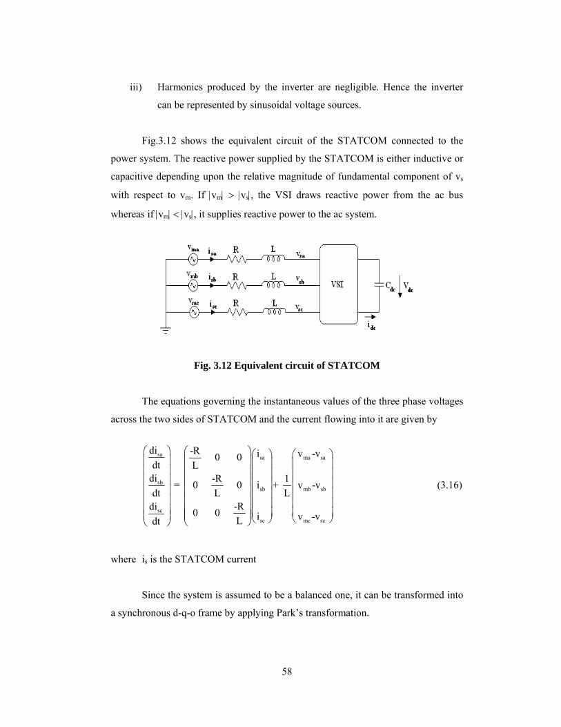
Fig.3.12 shows the equivalent circuit of the STATCOM connected to the
power system. The reactive power supplied by the STATCOM is either inductive or
capacitive depending upon the relative magnitude of fundamental component of vs
with respect to vm. If |vm| > |vs|, the VSI draws reactive power from the ac bus
whereas if |vm| < |vs|, it supplies reactive power to the ac system.
Fig. 3.12 Equivalent circuit of STATCOM
The equations governing the instantaneous values of the three phase voltages
across the two sides of STATCOM and the current flowing into it are given by
sa sa ma sa
sbsb mb sb
sc
sc mc sc
di -R i v -v0 0dt L
di -R 1 = 0 0 i + v -vdt L L
-Rdi 0 0 i v -vLdt
⎛ ⎞ ⎛ ⎞⎛ ⎞ ⎛ ⎞⎜ ⎟ ⎜ ⎟⎜ ⎟ ⎜ ⎟⎜ ⎟ ⎜ ⎟⎜ ⎟ ⎜ ⎟⎜ ⎟ ⎜ ⎟⎜ ⎟ ⎜ ⎟⎜ ⎟ ⎜ ⎟⎜ ⎟ ⎜ ⎟⎜ ⎟ ⎜ ⎟⎜ ⎟ ⎜ ⎟⎜ ⎟ ⎜ ⎟⎜ ⎟ ⎜ ⎟⎜ ⎟⎜ ⎟ ⎝ ⎠ ⎝ ⎠⎝ ⎠⎝ ⎠
(3.16)
where is is the STATCOM current
Since the system is assumed to be a balanced one, it can be transformed into
a synchronous d-q-o frame by applying Park’s transformation.
59
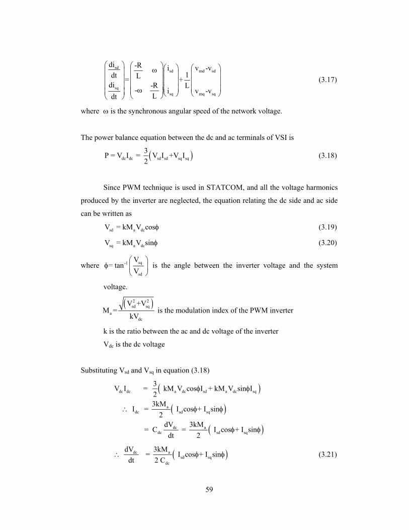
sdsd md sd
sqsq mq sq
di -R i v -vω 1dt L= +di -R L-ω i v -v
Ldt
⎛ ⎞ ⎛ ⎞⎛ ⎞ ⎛ ⎞⎜ ⎟ ⎜ ⎟⎜ ⎟ ⎜ ⎟⎜ ⎟ ⎜ ⎟⎜ ⎟ ⎜ ⎟⎜ ⎟ ⎜ ⎟⎜ ⎟ ⎜ ⎟⎜ ⎟⎜ ⎟ ⎝ ⎠ ⎝ ⎠⎝ ⎠⎝ ⎠
(3.17)
where ω is the synchronous angular speed of the network voltage.
The power balance equation between the dc and ac terminals of VSI is
( )dc dc sd sd sq sq3P = V I = V I +V I2
(3.18)
Since PWM technique is used in STATCOM, and all the voltage harmonics
produced by the inverter are neglected, the equation relating the dc side and ac side
can be written as
sd a dcV = kM V cosφ (3.19)
sq a dcV = kM V sinφ (3.20)
where sq-1
sd
V= tan
V⎛ ⎞
φ ⎜ ⎟⎝ ⎠
is the angle between the inverter voltage and the system
voltage.
( )2 2
sd sqa
dc
V +VM =
kV is the modulation index of the PWM inverter
k is the ratio between the ac and dc voltage of the inverter
Vdc is the dc voltage
Substituting Vsd and Vsq in equation (3.18)
( )
( )
( )
dc dc a dc sd a dc sq
adc sd sq
dc adc sd sq
3 V I = kM V cos I + kM V sin I23kM
I = I cos + I sin2
dV 3kM = C = I cos + I sin
dt 2
φ φ
∴ φ φ
φ φ
( )dc asd sq
dc
dV 3kM = I cos + I sin
dt 2 C∴ φ φ (3.21)
60
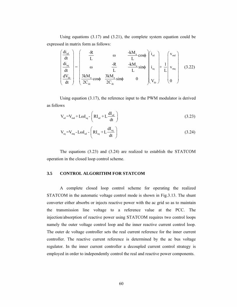
Using equations (3.17) and (3.21), the complete system equation could be
expressed in matrix form as follows:
sd a sd md
sq asq mq
a adc
dcdc dc
di -kM-R i vω cosdt L Ldi -kM-R 1 = ω sin i + vdt L L L
3kM 3kMdV cos sin 0 V 02C 2Cdt
⎛ ⎞⎛ ⎞ ⎛ ⎞ ⎛ ⎞φ⎜ ⎟⎜ ⎟ ⎜ ⎟ ⎜ ⎟⎜ ⎟⎜ ⎟ ⎜ ⎟ ⎜ ⎟⎜ ⎟⎜ ⎟ ⎜ ⎟ ⎜ ⎟φ⎜ ⎟⎜ ⎟ ⎜ ⎟ ⎜ ⎟⎜ ⎟⎜ ⎟ ⎜ ⎟ ⎜ ⎟⎜ ⎟⎜ ⎟ ⎜ ⎟ ⎜ ⎟φ φ⎜ ⎟ ⎜ ⎟ ⎝ ⎠⎝ ⎠⎝ ⎠ ⎝ ⎠
(3.22)
Using equation (3.17), the reference input to the PWM modulator is derived
as follows
sdsd md sq sd
dIV =V + LωI - RI + L
dt⎛ ⎞⎜ ⎟⎝ ⎠
(3.23)
sqsq mq sd sq
dIV =V -LωI - RI + L
dt⎛ ⎞⎜ ⎟⎝ ⎠
(3.24)
The equations (3.23) and (3.24) are realized to establish the STATCOM
operation in the closed loop control scheme.
3.5 CONTROL ALGORITHM FOR STATCOM
A complete closed loop control scheme for operating the realized
STATCOM in the automatic voltage control mode is shown in Fig.3.13. The shunt
converter either absorbs or injects reactive power with the ac grid so as to maintain
the transmission line voltage to a reference value at the PCC. The
injection/absorption of reactive power using STATCOM requires two control loops
namely the outer voltage control loop and the inner reactive current control loop.
The outer dc voltage controller sets the real current reference for the inner current
controller. The reactive current reference is determined by the ac bus voltage
regulator. In the inner current controller a decoupled current control strategy is
employed in order to independently control the real and reactive power components.

61
Fig. 3.13 Closed loop control scheme of STATCOM
A phase locked loop is used to determine the instantaneous angle θ of the
three-phase line voltage Vm sensed at bus B2 of Fig.3.11. The three-phase voltages
sensed at B2 and inverter currents are transformed into two-phase quantities using
Park’s transformation, which gives d – q axis voltage and current for the controller.
The d-axis reference current isd* obtained from the dc voltage controller is compared
with the actual d axis current and stabilized through PI controller to get the
equivalent d axis reference voltage. Similarly the actual q axis current iq is
compared with the reference current isq* derived from the ac voltage controller and
the error so obtained is stabilized through another PI controller to get the equivalent
q axis reference voltage. The parameters of these PI controllers are tuned in order to
minimize the integral square error (ISE) and integral time absolute error (ITAE).
The optimal parameters of PI controllers are tabulated in Table 3.3. Further the
equations (3.23) and (3.24) are realized in the inner current control loop in order to
obtain the reference wave for the PWM modulator.
62
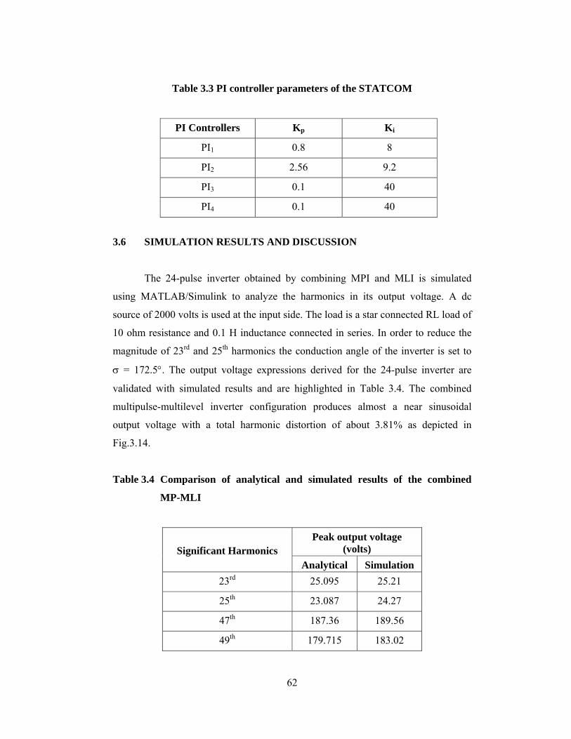
Table 3.3 PI controller parameters of the STATCOM
PI Controllers Kp Ki
PI1 0.8 8
PI2 2.56 9.2
PI3 0.1 40
PI4 0.1 40
3.6 SIMULATION RESULTS AND DISCUSSION
The 24-pulse inverter obtained by combining MPI and MLI is simulated
using MATLAB/Simulink to analyze the harmonics in its output voltage. A dc
source of 2000 volts is used at the input side. The load is a star connected RL load of
10 ohm resistance and 0.1 H inductance connected in series. In order to reduce the
magnitude of 23rd and 25th harmonics the conduction angle of the inverter is set to
σ = 172.5°. The output voltage expressions derived for the 24-pulse inverter are
validated with simulated results and are highlighted in Table 3.4. The combined
multipulse-multilevel inverter configuration produces almost a near sinusoidal
output voltage with a total harmonic distortion of about 3.81% as depicted in
Fig.3.14.
Table 3.4 Comparison of analytical and simulated results of the combined
MP-MLI
Peak output voltage (volts) Significant Harmonics
Analytical Simulation 23rd 25.095 25.21
25th 23.087 24.27
47th 187.36 189.56
49th 179.715 183.02
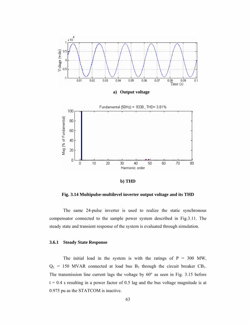
63
a) Output voltage
b) THD
Fig. 3.14 Multipulse-multilevel inverter output voltage and its THD
The same 24-pulse inverter is used to realize the static synchronous
compensator connected to the sample power system described in Fig.3.11. The
steady state and transient response of the system is evaluated through simulation.
3.6.1 Steady State Response
The initial load in the system is with the ratings of P = 300 MW,
QL = 150 MVAR connected at load bus B3 through the circuit breaker CB1.
The transmission line current lags the voltage by 60° as seen in Fig. 3.15 before
t = 0.4 s resulting in a power factor of 0.5 lag and the bus voltage magnitude is at
0.975 pu as the STATCOM is inactive.
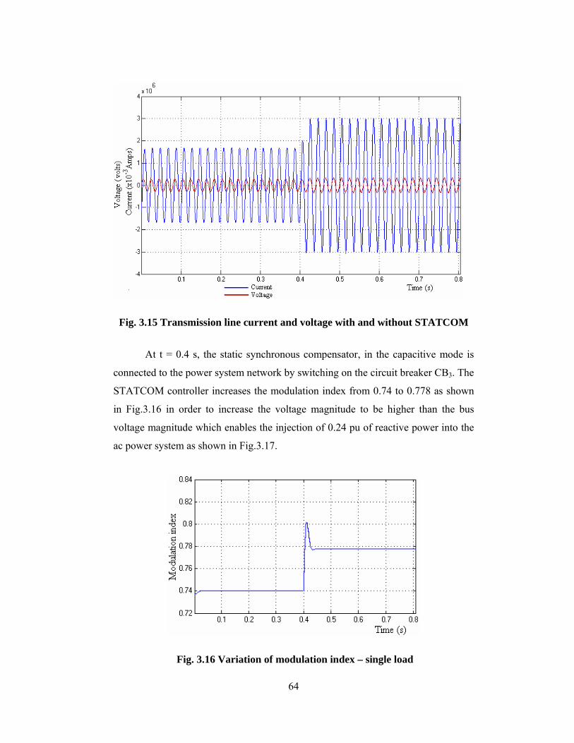
64
Fig. 3.15 Transmission line current and voltage with and without STATCOM
At t = 0.4 s, the static synchronous compensator, in the capacitive mode is
connected to the power system network by switching on the circuit breaker CB3. The
STATCOM controller increases the modulation index from 0.74 to 0.778 as shown
in Fig.3.16 in order to increase the voltage magnitude to be higher than the bus
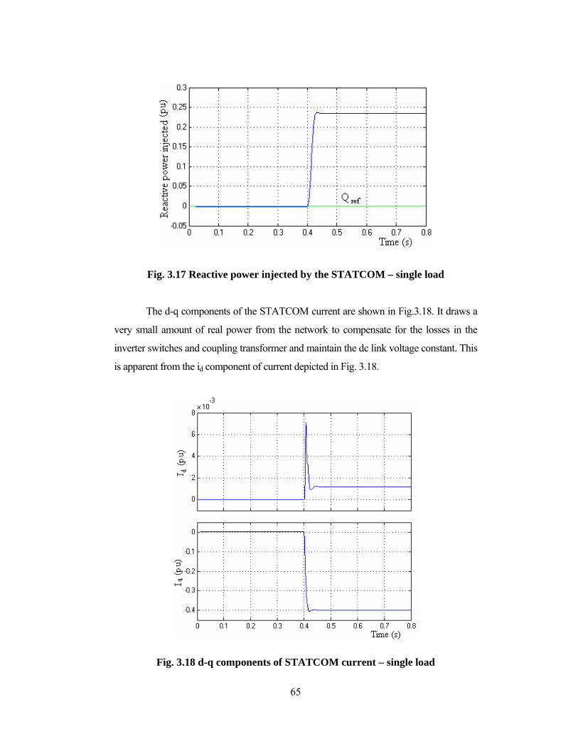
voltage magnitude which enables the injection of 0.24 pu of reactive power into the
ac power system as shown in Fig.3.17.
Fig. 3.16 Variation of modulation index – single load
65
Fig. 3.17 Reactive power injected by the STATCOM – single load
The d-q components of the STATCOM current are shown in Fig.3.18. It draws a
very small amount of real power from the network to compensate for the losses in the
inverter switches and coupling transformer and maintain the dc link voltage constant. This
is apparent from the id component of current depicted in Fig. 3.18.
Fig. 3.18 d-q components of STATCOM current – single load
66
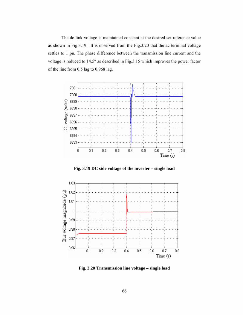
The dc link voltage is maintained constant at the desired set reference value
as shown in Fig.3.19. It is observed from the Fig.3.20 that the ac terminal voltage
settles to 1 pu. The phase difference between the transmission line current and the
voltage is reduced to 14.5° as described in Fig.3.15 which improves the power factor
of the line from 0.5 lag to 0.968 lag.
Fig. 3.19 DC side voltage of the inverter – single load
Fig. 3.20 Transmission line voltage – single load

67
3.6.2 Transient Response of the STATCOM under Variable Load
Figs.3.21-3.27 demonstrate the response of the STATCOM when load
variations are introduced at t = 0.4 s and t = 0.6 s respectively. Initially the inductive
Load (P = 300 MW, QL = 150 MVAR) is connected to the bus system through the
circuit breaker CB1. The bus voltage magnitude is 0.975 pu and the phase lag is 60°.
When the STATCOM is switched on at t = 0.2 s, it injects reactive power to the
system thereby increasing the bus voltage magnitude to 0.999 pu and reducing the
power factor to 0.968 lag (φ = 14.5° lag).
An additional inductive load of P = 300 MW, QL = 180 MVAR (Load 2) is
added to the power system at t = 0.4 s by switching ON the circuit breaker CB2. The
new inductive load connected to the bus system requires further reactive power
compensation. Therefore the STATCOM controller increases the modulation index
from 0.778 to 0.83 as shown in Fig.3.21 which provides a total reactive power
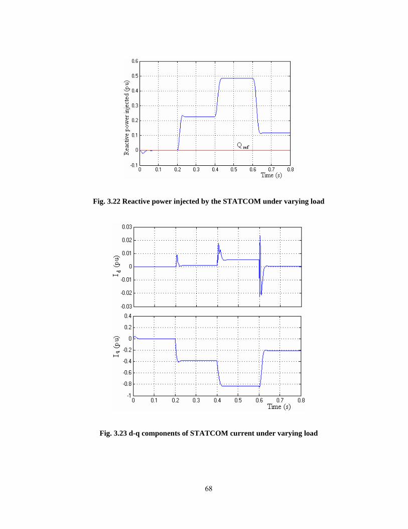
injection to 0.49 pu as seen in Fig.3.22. The corresponding variations in the d-q
components of the STATCOM current are clearly depicted in the Fig.3.23. In order
to maintain the dc link voltage to the desired reference value it draws still more real
power from the network and this result an increase in id component of STATCOM
current.
Fig. 3.21 Variation of modulation index under varying load
68
Fig. 3.22 Reactive power injected by the STATCOM under varying load
Fig. 3.23 d-q components of STATCOM current under varying load
69
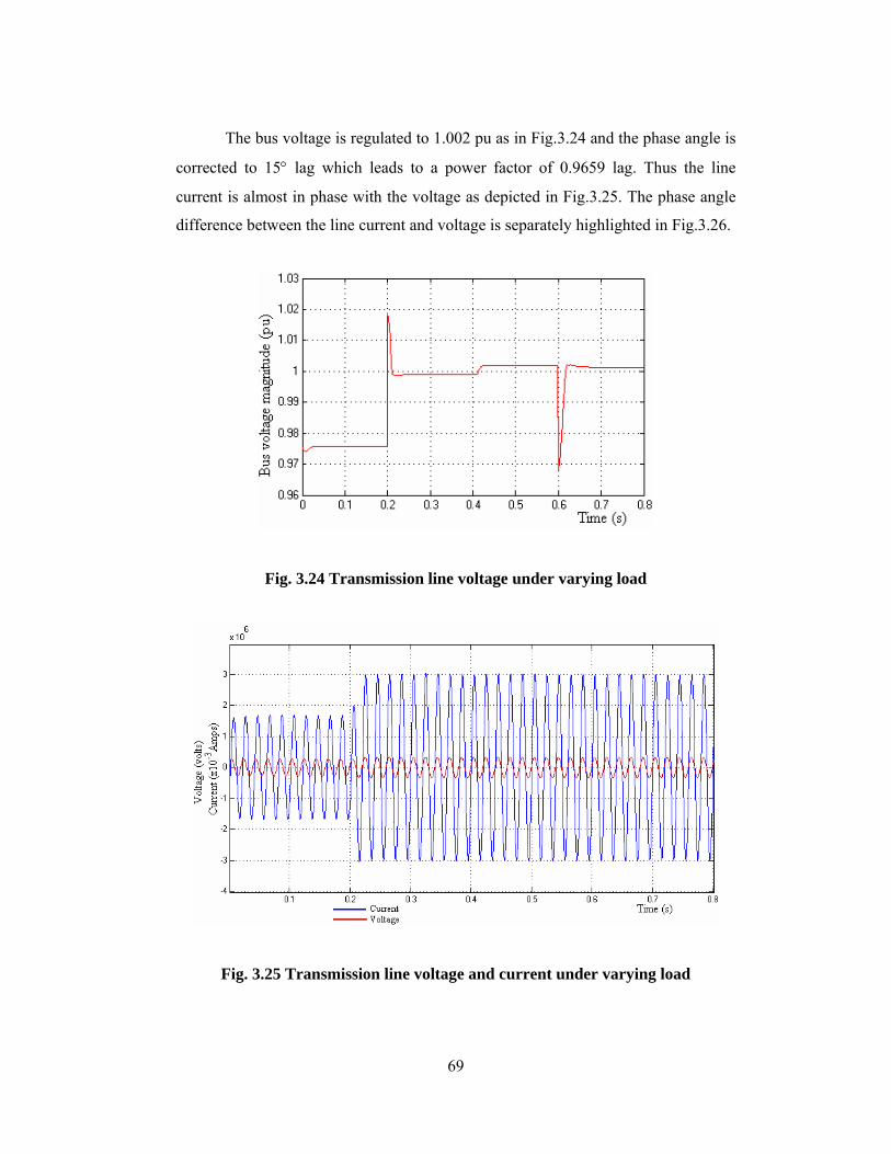
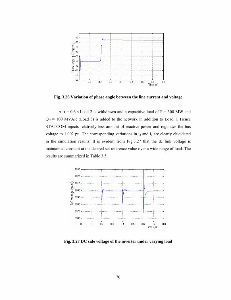
The bus voltage is regulated to 1.002 pu as in Fig.3.24 and the phase angle is
corrected to 15° lag which leads to a power factor of 0.9659 lag. Thus the line
current is almost in phase with the voltage as depicted in Fig.3.25. The phase angle
difference between the line current and voltage is separately highlighted in Fig.3.26.
Fig. 3.24 Transmission line voltage under varying load
Fig. 3.25 Transmission line voltage and current under varying load
70
Fig. 3.26 Variation of phase angle between the line current and voltage
At t = 0.6 s Load 2 is withdrawn and a capacitive load of P = 300 MW and
QC = 100 MVAR (Load 3) is added to the network in addition to Load 1. Hence
STATCOM injects relatively less amount of reactive power and regulates the bus
voltage to 1.002 pu. The corresponding variations in id and iq are clearly elucidated
in the simulation results. It is evident from Fig.3.27 that the dc link voltage is
maintained constant at the desired set reference value over a wide range of load. The
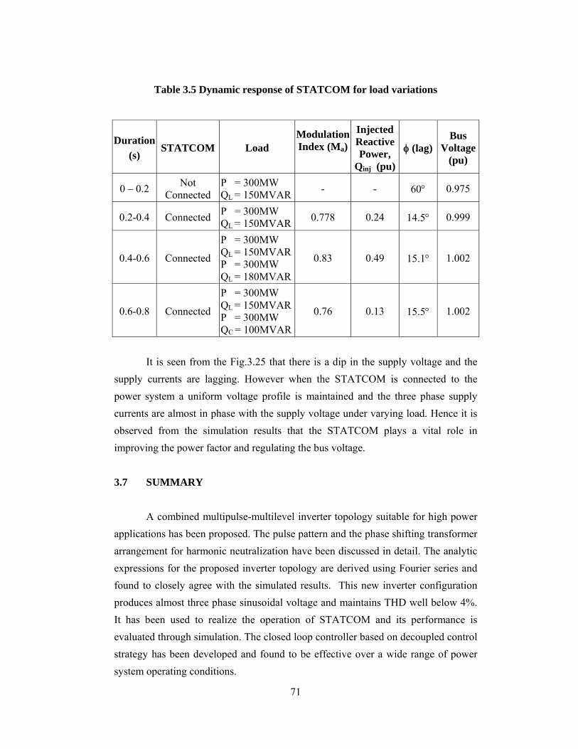
results are summarized in Table 3.5.
Fig. 3.27 DC side voltage of the inverter under varying load
71
Table 3.5 Dynamic response of STATCOM for load variations
Duration (s)
STATCOM Load Modulation Index (Ma)
Injected Reactive Power,
Qinj (pu)
φ (lag) Bus
Voltage (pu)
0 – 0.2 Not Connected
P = 300MW QL = 150MVAR - - 60° 0.975
0.2-0.4 Connected P = 300MW QL = 150MVAR 0.778 0.24 14.5° 0.999
0.4-0.6 Connected
P = 300MW QL = 150MVAR P = 300MW QL = 180MVAR
0.83 0.49 15.1° 1.002
0.6-0.8 Connected
P = 300MW QL = 150MVAR P = 300MW QC = 100MVAR
0.76 0.13 15.5° 1.002
It is seen from the Fig.3.25 that there is a dip in the supply voltage and the supply currents are lagging. However when the STATCOM is connected to the power system a uniform voltage profile is maintained and the three phase supply currents are almost in phase with the supply voltage under varying load. Hence it is observed from the simulation results that the STATCOM plays a vital role in improving the power factor and regulating the bus voltage. 3.7 SUMMARY A combined multipulse-multilevel inverter topology suitable for high power applications has been proposed. The pulse pattern and the phase shifting transformer arrangement for harmonic neutralization have been discussed in detail. The analytic expressions for the proposed inverter topology are derived using Fourier series and found to closely agree with the simulated results. This new inverter configuration produces almost three phase sinusoidal voltage and maintains THD well below 4%. It has been used to realize the operation of STATCOM and its performance is evaluated through simulation. The closed loop controller based on decoupled control strategy has been developed and found to be effective over a wide range of power system operating conditions.


![SCATTERING ANALYSIS OF PERIODIC ARRAYS USING COMBINED … · Fourier transform method (CG-FFT) [13], fast multipole algorithm (FMM) or multilevel fast multipole algorithm (MLFMA)](https://img.pdfslide.net/doc/110x75/60a8f556e81d373cf3227d18/scattering-analysis-of-periodic-arrays-using-combined-fourier-transform-method-cg-fft.jpg)