Embed Size (px)
Citation preview

CHAPTER 6
FSMD
6.1 INTRODUCTION
An FSMD (finite state machine with data path) combines an FSM and regular sequential circuits. The FSM, which is sometimes known as a control path, examines the external commands and status and generates control signals to specify operation of the regular sequential circuits, which are known collectively as a data path. The FSMD is used to implement systems described by RT(register transfer) methodology, in which the operations are specified as data manipulation and transfer among a collection of registers.
6.1.1 Single RT operation
An RT operation specifies data manipulation and transfer for a single destination register. It is represented by the notation
rdest + f(rsrcl, rsrc2, . . . , rsrcn)
where rdest is the destination register, rsrCl, rSrc2, and r,,,, are the source registers, and f ( .) specifies the operation to be performed. The notation indicates that the contents of the source registers are fed to the f ( . ) function, which is realized by a combinational circuit, and the result is passed to the input of the destination register and stored in the destination register at the next rising edge of the clock. Following are several representative RT operations:
0 ri + 0. A constant 0 is stored in the rl register. 0 rl +- ri. The content of the rl register is written back to itself.
FPGA Prototyping by VHDL Examples. By Pong P. Chu Copyright @ 2008 John Wiley & Sons, Inc.
127

128 FSMD
a m
I D- b-reg
clk
(a) Block diagram
clk A-1
7 x 5 a-reg 9
(b) Timing diagram
Figure 6.1 Block and timing diagrams of an RT operation.
0 r2 +- r2 >> 3. The r2 register is shifted right three positions and then written back
0 r2 c rl. The content of the r l register is transferred to the r2 register. 0 i c i + 1. The content of the i register is incremented by 1 and the result is written
0 d c sl + s2 + s3. The summation of the sl, s2, and s3 registers is written to the d
0 y + a*a. The a squared is written to the y register.
to itself.
back to itself.
register.
A single RT operation can be implemented by constructing a combinational circuit for the f (.) function and connecting the input and output of the registers. For example, consider the a + a-b+l operation. The f ( . ) function involves a subtractor and an incrementor. The block diagram is shown in Figure 6.l(a). For clarity, we use the -reg and n e x t suffixes to represent the input and output of a register. Note that an RT operation is synchronized by an embedded clock. The result from the f (.) function is not stored to the destination register until the next rising edge of the clock. The timing diagram of the previous RT operation is shown in Figure 6.l(b).
6.1.2 ASMD chart
A circuit based on the RT methodology specifies which RT operations should be executed in each step. Since an RT operation is done in a clock-by-clock basis, its timing is similar to a state transition of an FSM. Thus, an FSM is a natural choice to specify the sequencing

INTRODUCTION 129
r l t r l + r2 u r l t r l << 2
r l t r l state-reg
clk
(a) ASMD segment (b) Block diagram
Figure 6.2 Realization of an ASMD segment.
of an RT algorithm. We extend the ASM chart to incorporate RT operations and call it an ASMD (ASM with data path) chart. The RT operations are treated as another type of activity and can be placed where the output signals are used.
A segment of an ASMD chart is shown in Figure 6.2(a). It contains one destination register, r l , which is initialized with 8, added with content of the r 2 register, and then shifted left two positions. Note that the rl register must be specified in each state. When r l is not changed, the rl +- r l operation should be used to maintain its current content, as in the s3 state. In future discussion, we assume that r t r is the default RT operation for the r register and do not include it in the ASMD chart. Implementing the RT operations of an ASMD chart involves a multiplexing circuit to route the desired next value to the destination register. For example, the previous segment can be implemented by a 4-to-1 multiplexer, as shown in Figure 6.2(b). The current state (i.e., the output of the state register) of the FSM controls the selection signal of the multiplexer and thus chooses the result of the desired RT operation.
An RT operation can also be specified in a conditional output box, as the r 2 register shown in Figure 6.3(a). Depending on the a>b condition, the FSMD performs either r 2 +- r2+a or r 2 +- r2+b. Note that all operations are done in parallel inside an ASMD block. We need to realize the a>b, r2+a, and r2+b operations and use a multiplexer to route the desired value to r2 . The block diagram is shown in Figure 6.3(b).
6.1.3 Decision box with a register
The appearance of an ASMD chart is similar to that of a normal flowchart. The main difference is that the RT operation in an ASMD chart is controlled by an embedded clock signal and the destination register is updated when the FSMD exits the current ASMD block, but not within the block. The r + r-1 operation actually means that:
0 r n e x t <= r - reg - I ; 0 r - reg <= r n e x t at the rising edge of the clock (i.e., when the FSMD exits the
current block).

130 FSMD
-1 j d 4 -
: u-
I state-reg
(b) Block diagram
rl-reg >
Figure 6.3 Realization of an RT operation in a conditional output box.

CODE DEVELOPMENT OF AN FSMD 131
....................
r t r - I $ T F-
................... 1 (a) Use old value of r
(y r-next=O F+
T ................... 1
(b) Use new value of r
Figure 6.4 ASM block affected by a delayed store.
This “delayed store” may introduce subtle errors when a register is used in a decision box. Consider the FSMD segment in Figure 6.4(a). The r register is decremented in the state box and used in the decision box. Since the r register is not updated until the FSMD exits the block, the old content of r is used for comparison in the decision box. If the new value of r is desired, we should use the output of the combinational logic (i.e., r n e x t ) in the decision box (i.e., replace the r = O expression with rnext=O), as shown in Figure 6.4(b). Note that we use the : = notation, as in r n e x t : =r-i, to indicate the immediate assignment of r n e x t .
Block diagram of an FSMD The conceptual block diagram of an FSMD is divided into a data path and a control path, as shown in Figure 6.5. The data path performs the required RT operations. It consists of
0 Data registers: store the intermediate computation results 0 Functional units: perform the functions specified by the RT operations
Routing network: routes data between the storage registers and the functional units The data path follows the cont ro l signal to perform the desiredRT operations and generates the i n t e r n a l s t a t u s signal.
The control path is an FSM. As a regular FSM, it contains a state register, next-state logic, and output logic. It uses the external command signal and the data path’s s t a t u s signal as the input and generates the cont ro l signal to control the data path operation. The FSM also generates the ex te rna l s t a t u s signal to indicate the status of the FSMD operation.
Note that although an FSMD consists of two types of sequential circuits, both circuits are controlled by the same clock, and thus the FSMD is still a synchronous system.
6.2 CODE DEVELOPMENT OF AN FSMD
We use an improved debouncing circuit to demonstrate derivation of the FSMD code. Although the debouncing circuit in Section 5.3.2 uses an FSM and a timer (which is a regular sequential circuit), it is not based on the RT methodology because the two units are running independently and the FSM has no control over the timer. Since the 10-ms enable

132 FSMD
*
data input
- routing network - functional units - routing
network
- d q data > registers
command
internal status I I t control signal
. . . . . . . . . . . . . . , , . . . . . . . . , . . . . . . . . . . . . . . . . . . . . .
(I-.--
,
- ,
data output
next-state + logic -
external status
output > register logic
state
control path
Figure 6.5 Block diagram of an FSMD.
tick can be asserted at any time, the FSM does not know how much time has elapsed when the first tick is detected in the w a i t i - 1 or w a i t 0 - I state. Thus, the waiting period in this design is between 20 and 30 ms but is not an exact interval. This deficiency can be overcome by applying the RT methodology. In this section, we use this improved debouncing circuit to illustrate the FSMD code development.
6.2.1
With the RT methodology, we can use an FSM to control the initiation of the timer to obtain the exact interval. The ASMD chart is shown in Figure 6.6. The circuit is expanded to include two output signals: db-level , which is the debounced output, and db-tick, which is a one-clock-cycle enable pulse asserted at the zero-to-one transition. The z e r o and one states mean that the s w input has been stabilized for '0' and ' l ' , respectively. The w a i t l and w a i t 0 states are used to filter out short glitches. The s w signal must be stable for a certain amount of time or the transition will be treated as a glitch. The data path contains one register, q, which is 21 bits wide. Assume that the FSMD is originally in the z e r o state. When the s w input signal becomes ' 1 ', the FSMD moves to the w a i t I state and initializes q to "1 . . . 1". In the w a i t l state, the q decrements in each clock cycle. If s w remains as ' 1 ', the FSMD returns to this state repeatedly until q reaches "0 . . . 0 " and then moves to the one state.
Debouncing circuit based on RT methodology

CODE DEVELOPMENT OF AN FSMD 133
. . . . . . . . . . . . . . . . . . . . . . . . . . . . . . . . . . . . . . . .
...
-
q-next := q- 3 q tq -nex t
T
db-tick <= 1 0
d b-level<= 1
T
q -1 ... 1 0 I-
....
wait0
d b-level<= 1
T
Figure 6.6 ASMD chart of a debouncing circuit.

134 FSMD
Recall that the 50-MHz (i.e., 20-11s period) system clock is used on the prototyping board. Since the FSMD stays in the waitl state for 2’l clock cycles, it is about 40 ms (i.e., 221*20 ns). We can modify the initial value of the q register to obtain the desired wait interval.
There are two ways to derive the HDL code, one with explicit description of the data path components and the other with implicit description of the data path components.
6.2.2 Code with explicit data path components
The first approach to FSMD code development is to separate the control FSM and the key data path components. From an ASMD chart, we first identify the key components in the data path and the associated control signals and then describe these components in individual code segments.
The key data path component of the debouncing circuit ASMD chart is a custom 21-bit decrement counter that can:
0 Be initialized with a specific value Count downward or pause Assert a status signal when the counter reaches 0
We can create a binary counter with a q-load signal to load the initial value and a q-dec signal to enable the counting. The counter also generates a q-zero status signal, which is asserted when the counter reaches zero. The complete data path is composed of the q register and the next-state logic of the custom decrement counter. A comparison circuit is included to generate the q-zero status signal. The control path consists of an FSM, which takes the s w input and the q-zero status and asserts the control signals, q-load and q-dec, according to the desired action in the ASMD chart. The HDL code follows the data path specification and the ASMD chart, and is shown in Listing 6.1.
Listing 6.1 Debouncing circuit with an explicit data path component
l i b r a r y ieee; use ieee. std-logic-1164. a l l ; use ieee . numeric-std. a l l ; e n t i t y debounce i s
s p o r t ( c l k , reset: in std-logic; s w : in std-logic; db-level , db-tick: out std-logic
) ; mend debounce ;
a r c h i t e c t u r e exp-fsmd-arch of debounce i s c o n s t a n t N: integer:=21; -- f i l t e r of 2 ^ N * 2 0 n s = 40ms type state-type i s (zero, wait0, one, waitl);
s i g n a l q-reg , q-next : unsigned(N-1 downto 0) ; s i g n a l q-load , q-dec , q-zero : std-logic ;
-- FSMD s t a t e C? d a t a r e g i s t e r s
begin
IS s i g n a l state-reg , state-next : state-type;
begin
zo p r o c e s s (clk ,reset)
if reset=’l’ then state-reg <= zero;

CODE DEVELOPMENT OF AN FSMD 135
q - r e g <= ( o t h e r s = > ’ O ’ ) ;
s t a t e - r e g <= s t a t e - n e x t ; q - r e g <= q - n e x t ;
e l s i f ( c l k ’ e v e n t and c l k = ’ l ’ ) then
end i f ; end p r o c e s s ;
30
-- FSMD d a t a p a t h ( c o u n t e r ) n e x t - s t a t e l o g i c q - n e x t <= ( o t h e r s = > ’ 1 ’ ) when q - l o a d = 1 ’ e l s e
q - r e g - 1 when q - d e c = ’ l J e l s e q - r e g ;
35 q - z e r o <= ’ 1 ’ when q - n e x t = o e l s e j 0 ’ ;
-- FSMD c o n t r o l p a t h n e x t - s t a t e l o g i c p r o c e s s ( s t a t e - r e g , s w , q - z e r o ) beg in
40 q - l o a d <= ’ 0 ’ ; q - d e c <= ’ 0 ’ ; d b - t i c k <= ’ 0 ’ ; s t a t e - n e x t <= s t a t e - r e g ; case s t a t e - r e g i s
55
i 0
5
when z e r o => d b - l e v e l <= > O J ; i f ( s w = ’ l ’ ) then
s t a t e - n e x t <= w a i t l ; q - l o a d <= ’ 1 ’ ;
end i f ; when w a i t l = >
d b - l e v e l <= ’ 0 ’ ; i f ( s w = ’ l ’ ) then
q - d e c <= ’ 1 ’ ; i f ( q - z e r o = ’ l ’ ) then
s t a t e - n e x t (= o n e ; d b - t i c k <= ’1’;
end i f ;
s t a t e - n e x t <= z e r o ; e l s e -- s w = ’ O ’
end i f ;
d b - l e v e l <= ’ 1 ’ ; i f ( s w = ’ O J ) then
when one = >
s t a t e - n e x t <= w a i t 0 ; q - l o a d <= ’1’;
end i f ; when w a i t O = >
d b - l e v e l <= ’ 1 ’ ; i f ( s w = ’ O ’ ) then
q - d e c <= ’ 1 ’ ; i f (q-zero=’l’) then
end i f ;
s t a t e - n e x t <= o n e ;
s t a t e - n e x t <= z e r o ;
e l s e -- sw= ’ 1 ’

136 FSMD
end i f ; end c a s e ;
end p r o c e s s ; 80 end e x p - f s m d - a r c h ;
6.2.3 Code with implicit data path components
An alternative coding style is to embed the RT operations within the FSM control path. Instead of explicitly defining the data path components, we just list RT operations with the corresponding FSM state. The code of the debouncing circuit is shown in Listing 6.2.
15
21
30
35
Listing 6.2 Debouncing circuit with an implicit data path component
a r c h i t e c t u r e imp-f s m d - a r c h of d e b o u n c e i s c o n s t a n t N: i n t e g e r : = 2 1 ; -- f i l t e r o f 2 ^ N * 2 0 n s = 4 0 m s type s t a t e - t y p e i s ( z e r o , w a i t 0 , o n e , w a i t l ) ; s i g n a l s t a t e - r e g , s t a t e - n e x t : s t a t e - t y p e ;
s s i g n a l q - r e g , q - n e x t : u n s i g n e d ( N - 1 downto 0 ) ; begin
-- FSMD s t a t e C? d a t a r e g i s t e r s p r o c e s s ( c l k , r e s e t ) beg in
10 i f r e s e t = 1 ’ then s t a t e - r e g <= z e r o ; q - r e g <= ( o t h e r s = > ’ O ’ ) ;
s t a t e - r e g <= s t a t e - n e x t ; q - r e g <= q - n e x t ;
e l s i f ( c l k ’ e v e n t and c l k = ’ l ’ ) then
end i f ; end p r o c e s s ; -- n e x t - s t a t e l o g i c & d a t a p a t h f u n c t i o n a l u n i t s / r o u t i n g p r o c e s s ( s t a t e - r e g , q - r e g , s w , q - n e x t )
20 beg in s t a t e - n e x t <= s t a t e - r e g ; q - n e x t <= q - r e g ; d b - t i c k <= ’ 0 ’ ; c a s e s t a t e - r e g i s
when z e r o = > d b - l e v e l <= ’ 0 ’ ; i f ( s w = ’ l ’ ) then
s t a t e - n e x t <= w a i t l ; q - n e x t <= ( o t h e r s = > ’ l ’ ) ;
end i f ; when w a i t l = >
d b - l e v e l <= ’ 0 ’ ; i f ( s w = ’ l ’ ) then
q - n e x t <= q - r e g - 1; i f ( q - n e x t = O ) then
s t a t e - n e x t <= o n e ; d b - t i c k <= ’ 1 ’ ;
end i f ;
s t a t e - n e x t <= z e r o ; e l s e -- s w = ’ O ’

CODE DEVELOPMENT OF AN FSMD 137
55
end i f ;
db-level <= ’1 ’ ; i f (sw=’O’) then
when one =>
state-next <= wait0; q-next <= ( o t h e r s = > ’ l ’ ) ;
end i f ; when waitO=>
db-level <= ’ 1 ’ ; i f (sw=’O’) then
q-next <= q-reg - 1; i f (q-next=O) then
end i f ;
state-next <= one;
state-next <= zero;
e l s e -- s w = ’ l ’
end i f ; end c a s e ;
end p r o c e s s ; 60 end imp-f smd-arch ;
The code consists of a memory segment and a combinational logic segment. The former contains the state register of the FSM and the data register of the data path. The latter basically specifies the next-state logic of the control path FSM. Instead of generating control signals, the next data register values are specified in individual states. The next-state logic of the data path, which consists of functional units and routing network, is created accordingly.
6.2.4 Comparison
Code with implicit data path components essentially follows the ASMD chart. We just convert the chart to an HDL description. Although this approach is simpler and more descriptive, we rely on synthesis software for data path construction and have less control. This can best be explained by an example. Consider the ASMD segment in Figure 6.7. The implicit description becomes
c a s e when sl
dl-next <= a * b ; . . .
when s 2 d2-next <= b * c ; . . .
when s3 d3-next <= a * c ; . . .
end c a s e ;
The synthesis software may infer three multipliers. Since a combinational multiplier is a complex circuit, it is more efficient to share the circuit. We can use explicit description to isolate the multiplier:
case when sl

138 FSMD
Figure 6.7 ASMD segment with sharing opportunity.
in1 <= a; in2 <= b ; dl-next <= m-out;
when s 2 in1 <= b ; i n 2 <= c ; d2-next <= m-out;
when s3 in1 <= a ; in2 <= c ; d3-next <= m-out;
end c a s e ; __ e x p l i c i t d e s c r i p t i o n of a s i n g l e m u l t i p l i e r m-out <= in1 * in2;
The code ensures that only one multiplier is inferred during synthesis. The implicit and explicit descriptions can be mixed for a complex FSMD design. We frequently isolate and extract complex data path components for code clarity and efficiency.
6.2.5 Testing circuit
The debouncing testing circuit discussed in Section 5.3.3 can be used to verify operation of the new design. Since the revised debouncing circuit's outputs include a one-clock-cycle tick signal, no edge detector is needed after the debouncing circuit. The revised block

CODE DEVELOPMENT OF AN FSMD 139
- btn(1) - level tick - en q - edge
> detector >counter 4- hex0 sseg sseg - hex1 an - an
Figure 6.8 Debouncing testing circuit.
diagram is shown in Figure 6.8, and the corresponding code is shown in Listing 6.3.
Listing 6.3
l i b r a r y ieee; use ieee, std-logic-1164. a l l ; use ieee. numeric-std. a l l ; e n t i t y debounce-test i s
Verification circuit for a debouncing circuit
5 p o r t ( clk: i n std-logic; btn: i n std-logic-vector (3 downto 0) ; an: o u t std-logic-vector ( 3 downto 0) ; sseg: out std-logic-vector (7 downto 0)
lo ) ; end debounce-test ;
sw db-tick
> clk - debouncing
30
en q disp-mux-hex
> counter reset
a r c h i t e c t u r e arch of debounce-test i s s i g n a l ql-reg , ql-next : unsigned ( 7 downto 0) ;
I S s i g n a l qO-reg, q0-next : unsigned ( 7 downto 0) ; s i g n a l b-count , d-count : std-logic-vector (7 downto 0 ) ; s i g n a l btn-reg : std-logic; s i g n a l db-tick , btn-tick , clr : std-logic;
b e g i n 20 -- i n s t a n t i a t e d e b o u n c i n g c i r c u i t
db-unit : e n t i t y work. debounce (f smd-arch) p o r t map(
clk=>clk, reset=>'O', sw=>btn(l) , db-level=> o p e n , db-tick=>db-tick
1 ; _- i n s t a n t i a t e h e x d i s p l a y t i m e - m u 1 t i p l x i n g c i r c u i t disp-unit : e n t i t y work. disp-hex-mux
p o r t map( clk=>clk , reset=> ' 0 ' , hex3=>b_count (7 downto 4), hex2=>b_count (3 downto 0 1 , hexl=>d-count ( 7 downto 41, hexO=>d-count ( 3 downto 0 1 , dp-in=>"lOll", an=>an, sseg=>sseg
) ;
-- e d g e d e t e c t i o n c i r c u i t f o r u n - d e b o u n c e d i n p u t

140 FSMD
____________________----------------------------- -- ____________________--_--------------------- p r o c e s s (clk) beg in
40 i f (clk event and clk= ’ 1 ’ ) then btn-reg <= btn(1);
end i f ; end p r o c e s s ; btn-tick <= (not btn-reg) and btn(1);
45
. . . . . . . . . . . . . . . . . . . . . . . . . . . . . . . . . . . . . . . . . . . . . . . . . . .
-_ t w o c o u n t e r s
clr <= btn(0);
beg in
. . . . . . . . . . . . . . . . . . . . . . . . . . . . . . . . . . . . . . . . . . . . . . . . . . .
j n p r o c e s s (clk)
i f (clk ’ event and clk= ’ 1 ’ ) then ql-reg <= ql-next; q0-reg <= q0-next;
55 end i f ; end p r o c e s s ; __ n e x t - s t a t e logic f o r t h e c o u n t e r ql-next <= ( o t h e r s = > ’ O ’ ) when clr=’l’ e l s e
ql-reg f 1 when btn-tick=’l’ e l s e 60 ql-reg ;
q0-next <= ( o t h e r s = > ’ O ’ ) when clr=’i’ e l s e q0-reg + 1 when db-tick=’l’ e l s e qO-reg;
-_ c o u n t e r o u t p u t 65 b-count <= std-logic-vector(ql-reg);
d-count <= s t d - l o g i c - v e c t o r ( q 0 - r e g ) ; end arch;
6.3 DESIGN EXAMPLES
6.3.1 Fibonacci number circuit
The Fibonacci numbers constitute a sequence defined as
i f i = O i f i = 1 if i > 1 f i b ( i - 1) + f i b ( i - 2)
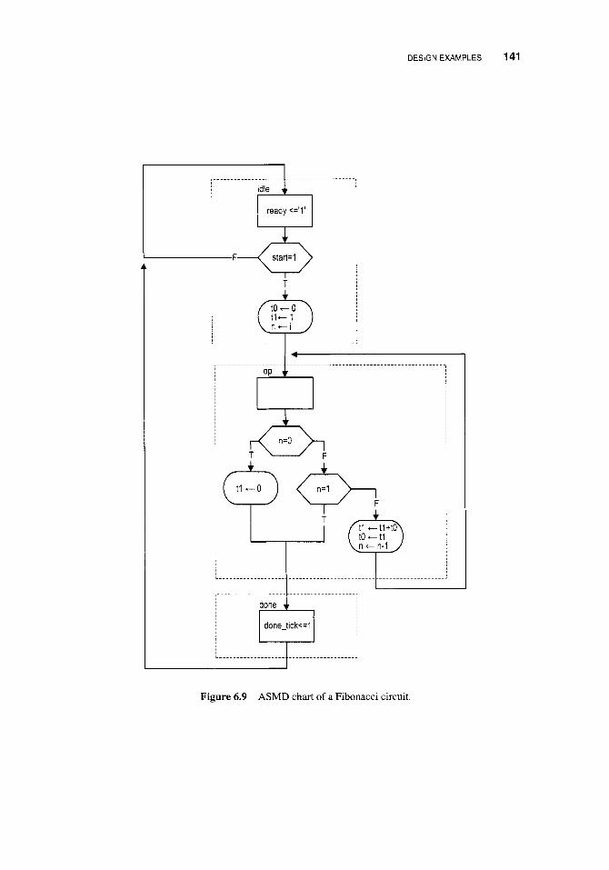
One way to calculate f i b ( i ) is to construct the function iteratively, from 0 to the desired i. This approach requires two temporary registers to store the two most recently calculated values (i.e., f i b ( i - 1) and f i b ( i - 2)) and one index register to keep track of the number of iterations. The ASMD chart is shown in Figure 6.9, in which t l and t O are temporary storage registers and n is the index register. In addition to the regular data input and output signals, i and f , we include a command signal, s tart , which signals the beginning of operation, and two status signals: ready, which indicates that the circuit is idle and ready to take new input, and done-tick, which is asserted for one clock cycle when the operation
DESIGN EXAMPLES 141
ready <='I '
-F
.............................................................
Figure 6.9 ASMD chart of a Fibonacci circuit.
142 FSMD
is completed. Since this circuit, like many other FSMD designs, is probably a part of a larger system, these signals are needed to interface with other subsystems.
The ASMD chart has three states. The i d l e state indicates that the circuit is currently idle. When s ta r t is asserted, the FSMD moves to the op state and loads initial values to three registers. The t O and t l registers are loaded with 0 and 1, which represent f i b ( 0 ) and f i b ( l), respectively. The n register is loaded with i, the desired number of iterations.
The main computation is iterated through the op state by three RT operations: 0 t i t t i + t o 0 t o + ti 0 n t n - 1
The first two RT operations obtain a new value and store the two most recently calculated values in t i and t o . The third RT operation decrements the iteration index. The iteration ended when n reaches 1 or its initial value is 0 (i.e., f i b ( 0 ) ) . Unlike a regular flowchart, the operations in an ASMD block can be performed concurrently in the same clock cycle. We put all comparison and RT operations in the op state to reduce the computation time. Note that the new values of the t 1 and t O registers are loaded at the same time when the FSMD exits the op state (i.e., at the next rising edge of the clock). Thus, the original value of t l , not t l+tO, is stored to t o . The purpose of the done state is to generate the one-clock-cycle done-tick signal to indicate completion of the computation. This state can be omitted if this status signal is not needed.
The code follows the ASMD chart and is shown in Listing 6.4. Note that the Fibonacci function grows rapidly and the output signal should be wide enough to accommodate the desired result.
Listing 6.4 Fibonacci number circuit
l i b r a r y ieee; use ieee. std-logic-1164, a l l ; use ieee. numeric-std. a l l ; e n t i t y fib i s
5 port ( clk, reset: in std-logic; start : in std-logic; i : in std-logic-vector (4 downto 0) ; ready, done-tick: out std-logic;
10 f : out std-logic-vector ( 1 9 downto 0 )
) ; end fib;
a r c h i t e c t u r e arch of fib i s 15 type state-type i s (idle,op,done);
s i g n a l state-reg , state-next : state-type; s i g n a l to-reg , to-next : unsigned (19 downto 0 ) ; s i g n a l tl-reg, tl-next : unsigned(l9 downto 0 ) ; s i g n a l n-reg , n-next : unsigned (4 downto 0) ;
-- f s m d s t a t e a n d d a t a r e g i s t e r s p r o c e s s (clk, reset) begin
20 beg in
i f reset=’l’ then 25 state-reg <= idle;
to-reg <= ( o t h e r s = > ’ O ’ ) ;

DESIGN EXAMPLES 143
30
t i - r e g <= ( o t h e r s = > ’ O ’ ) ; n - r e g <= ( o t h e r s = > ’ O ’ ) ;
s t a t e - r e g <= s t a t e - n e x t ; t 0 - r e g <= t o - n e x t ; t l - r e g <= t l - n e x t ; n - r e g <= n - n e x t ;
e I s i f ( c l k ’ e v e n t and c l k = ’ 1 ’ ) then
end i f ; 35 end p r o c e s s ;
-- f s m d n e x t - s t a t e l o g i c p r o c e s s ( s t a t e - r e g , n - r e g , t o - r e g , t l - r e g , s t a r t , i n - n e x t )
40
45
begin r e a d y < = ’ O ’ ; d o n e - t i c k <= ’ 0 ’ ; s t a t e - n e x t <= s t a t o - n e x t <= t o - r e g t l - n e x t <= t l - r e g n - n e x t <= n - r e g ; case s t a t e - r e g i s
when i d l e =>
e - r e g ;
50
55
M1
65
r e a d y <= ’ 1 ’ ; i f s t a r t = ’ l ’ then
t o - n e x t <= ( o t h e r s = > ’ O ’ ) ; t i - n e x t <= ( 0 = > ’ 1 ’ , o t h e r s = > ’ O ’ ) ; n - n e x t <= u n s i g n e d ( i ) ; s t a t e - n e x t <= o p ;
end i f ; when op =>
i f n-reg=O then t i - n e x t <= ( o t h e r s = > ’ O ’ ) ; s t a t e - n e x t <= d o n e ;
s t a t e - n e x t <= d o n e ;
t l - n e x t <= t l - r e g + t o - r e g ; t o - n e x t <= t l - r e g ; n - n e x t <= n - r e g - 1;
e l s i f n - r e g = l then
e l s e
end i f ; when done = >
d o n e - t i c k <= ’ 1 ’ ; s t a t e - n e x t <= i d l e ;
end c a s e ; end p r o c e s s ;
f <= std-logic-vector(tl-reg); 70 -- o u t p u t
end a r c h ;
6.3.2 Division circuit
Because of complexity, the division operator cannot be synthesized automatically. We use an FSMD to implement the long-division algorithm in this subsection. The algorithm is illustrated by the division of two 4-bit unsigned integers in Figure 6.10. The algorithm can

144 FSMD
rh
divisor
0 0 11 0 - quotient 0 0 1 0 1 0 0 0 0 1 10 1 - dividend
0000 0001 0000 0011
rI
Figure 6.10 Long division of two 4-bit unsigned integers.
Figure 6.11 Sketch of division circuit’s data path.
be summarized as follows: 1. Double the dividend width by appending 0’s in front and align the divisor to the
leftmost bit of the extended dividend. 2. If the corresponding dividend bits are greater than or equal to the divisor, subtract the
divisor from the dividend bits and make the corresponding quotient bit 1. Otherwise, keep the original dividend bits and make the quotient bit 0.
3. Append one additional dividend bit to the previous result and shift the divisor to the right one position.
4. Repeat steps 2 and 3 until all dividend bits are used. The sketch of the data path is shown in Figure 6.11. Initially, the divisor is stored in the
d register and the extended dividend is stored in the rh and rl registers. In each iteration, the rh and rl registers are shifted to the left one position. This corresponds to shifting the divisor to the right of the previous algorithm. We can then compare rh and d and perform subtraction if r h is greater than or equal to d. When r h and rl are shifted to the left, the rightmost bit of rl becomes available. It can be used to store the current quotient bit. After

DESIGN EXAMPLES 145
we iterate through all dividend bits, the result of the last subtraction is stored in r h and becomes the remainder of the division, and all quotients are shifted into rl.
The ASMD chart of the division circuit is somewhat similar to that of the previous Fibonacci circuit. The FSMD consists of four states, i d l e , op, l a s t , and done. To make the code clear, we extract the compare and subtract circuit to separate code segments. The main computation is performed in the op state, in which the dividend bits and divisor are compared and subtracted and then shifted left 1 bit. Note that the remainder should not be shifted in the last iteration. We create a separate state, last, to accommodate this special requirement. As in the preceding example, the purpose of the done state is to generate a one-clock-cycle done-t i ck signal to indicate completion of the computation. The code is shown in Listing 6.5.
Listing 6.5 Division circuit
l i b r a r y i e e e ; use i e e e . s t d - l o g i c - 1 1 6 4 . a l l ; use i e e e . n u m e r i c - s t d . a l l ; e n t i t y d i v i s
5 g e n e r i c ( W : C B I T : i n t e g e r : = 4 -- CBIT=logZ ( W ) + l
i n t e g e r : = 8 ;
1 ; port (
10 c l k , r e s e t : in s t d - l o g i c ; s t a r t : in s t d - l o g i c ; d v s r , d v n d : i n s t d - l o g i c - v e c t o r (W-1 downto 0 ) ; r e a d y , d o n e - t i c k : out s t d - l o g i c ; q u o , r m d : out s t d - l o g i c - v e c t o r (W-1 downto 0)
15 ) ;
end d i v ;
a r c h i t e c t u r e a r c h of d i v i s type s t a t e - t y p e i s ( i d l e , o p , l a s t , d o n e ) ;
s i g n a l r h - r e g , r h - n e x t : u n s i g n e d ( W - 1 downto 0) ; s i g n a l r l - r e g , r l - n e x t : s t d - l o g i c - v e c t o r (W-1 downto 0) ; s i g n a l r h - t m p : u n s i g n e d ( W - 1 downto 0) ; s i g n a l d - r e g , d - n e x t : u n s i g n e d ( W - 1 downto 0 ) ;
s i g n a l q - b i t : s t d - l o g i c ;
-- f s m d s t a t e a n d d a t a r e g i s t e r s p r o c e s s ( c l k , r e s e t )
x s i g n a l s t a t e - r e g , s t a t e - n e x t : s t a t e - t y p e ;
25 s i g n a l n - r e g , n - n e x t : u n s i g n e d ( C B 1 T - 1 downto 0) ;
beg in
30 beg in i f r e s e t = ’ l ’ then
s t a t e - r e g <= i d l e ; r h - r e g <= ( o t h e r s = > ’ 0 ’ ) ; r l - r e g <= ( o t h e r s = > ’ O ’ ) ; d - r e g <= ( o t h e r s = > ’ O ’ ) ; n - r e g <= ( o t h e r s = > ’ 0 ’ ) ;
s t a t e - r e g <= s t a t e - n e x t ; r h - r e g <= r h - n e x t ;
e l s i f ( c l k ’ e v e n t and c l k = ’ l ’ ) then

146 FSMD
40 r l - r e g <= r l - n e x t ; d - r e g <= d - n e x t ; n - r e g <= n - n e x t ;
end i f ; end p r o c e s s ;
-- f s m d n e x t - s t a t e l o g i c and d a t a p a t h l o g i c p r o c e s s ( s t a t e - r e g , n - r e g , r h - r e g , r l - r e g , d - r e g ,
s t a r t , d v s r , dvnd , q - b i t , rh- tmp , n - n e x t ) beg in
45
50 r e a d y < = ’ O ’ ; d o n e - t i c k <= ’ 0 ’ ; s t a t e - n e x t <= s t a t e - r e g ; r h - n e x t <= r h - r e g ; r l - n e x t <= r l - r e g ;
55
60
65
70
75
80
85
90
d - n e x t <= d - r e g ; n - n e x t <= n - r e g ; c a s e s t a t e - r e g i s
when i d l e = > r e a d y <= ’1’; i f s t a r t = ’ l ’ then
r h - n e x t <= ( o t h e r s = > ’ O ’ ) ; r l - n e x t <= d v n d ; __ d i v i d e n d d - n e x t <= u n s i g n e d ( d v s r 1 ; __ d i v i s o r n - n e x t <= t o - u n s i g n e d ( W + l , CBIT); -- i n d e x s t a t e - n e x t <= o p ;
end i f ; when op =>
__ s h i f t r h and r l l e f l r l - n e x t <= r l - r e g ( W - 2 downto 0 ) & q - b i t ; r h - n e x t <= rh- tmp(W-2 downto 0 ) & r l - r e g ( W - 1 ) ; - - d e c r e a s e i n d e x n - n e x t <= n - r e g - 1; i f ( n - n e x t = l ) then
end i f ;
r l - n e x t <= r l - r e g ( W - 2 downto 0 ) & q - b i t ; r h - n e x t <= r h - t m p ; s t a t e - n e x t <= d o n e ;
s t a t e - n e x t <= i d l e ; d o n e - t i c k <= ’ 1 ’ ;
s t a t e - n e x t <= l a s t ;
when l a s t => -- l a s t i t e r a t i o n
when done = >
end c a s e ; end p r o c e s s ;
__ c o m p a r e and s u b t r a c t p r o c e s s ( r h - r e g , d - r e g ) beg in
i f r h - r e g >= d - r e g then rh- tmp <= r h - r e g - d - r e g ; q - b i t <= ’ 1 ’ ;
e l s e

DESIGN EXAMPLES 147
rh-tmp <= rh-reg; q-bit <= ' 0 ' ;
9 F end i f ; end p r o c e s s ;
__ o u t p u t quo <= rl-reg;
100 rmd <= std-logic-vector (rh-reg) ; end arch;
6.3.3 Binary-to-BCD conversion circuit
We discussed the BCD format in Section 4.5.2. In this format, a decimal number is rep- resented as a sequence of 4-bit BCD digits. A binary-to-BCD conversion circuit converts a binary number to the BCD format. For example, the binary number "0010 0000 0000" becomes "0101 0001 0010" (i.e., 51210) after conversion.
The binary-to-BCD conversion can be processed by a special BCD shift register, which is divided into 4-bit groups internally, each representing a BCD digit. Shifting a BCD sequence to the left requires adjustment if a BCD digit is greater than 910 after shifting. For example, if a BCD sequence is "0001 01 11" (i.e., 1710), it should become "001 1 0100" (i.e., 3410) rather than "0010 11 10". The adjustment requires subtracting 1010 (i.e., I l l O l O " ) from the right BCD digit and adding 1 (which can be considered as a carry-out) to the next BCD digit. Note that subtracting 1010 is equivalent to adding 610 for a4-bit binary number. Thus, the foregoing adjustment can also be achieved by adding 610 to the right BCD digit. The carry-out bit is generated automatically in this process.
In the actual implementation, it is more efficient to first perform the necessary adjustment on a BCD digit and then shift. We can check whether a BCD digit is greater than 410 and, if this is the case, add 310 to the digit. After all the BCD digits are corrected, we can then shift the entire register to the left one position. A binary-to-BCD conversion circuit can be constructed by shifting the binary input to a BCD shift register bit by bit, from MSB to LSB .
1.
2.
3.
[ts operation can be summarized as follows: For each 4-bit BCD digit in a BCD shift register, check whether the digit is greater than 4. If this is the case, add 310 to the digit. Shift the entire BCD register left one position and shift in the MSB of the input binary sequence to the LSB of the BCD register. Repeat steps 1 and 2 until all input bits are used.
The conversion process of a 7-bit binary input, "1 11 11 11" (i.e., 12710), is demonstrated in Table 6.1.
The code of a 13-bit conversion circuit is shown in Listing 6.6. It uses a simple FSMD to control the overall operation. When the start signal is asserted, the binary input is stored into the p2s register. The FSM then iterates through the 13 bits, similar to the process described in previous examples. Four adjustment circuits are used to correct the four BCD digits. For clarity, they are isolated from the next-state logic and described in a separate code segment.
Listing 6.6 Binary-to-BCD conversion circuit
l i b r a r y ieee; use ieee. std-logic-1164. a l l ; use ieee. numeric-std. a l l ;

148 FSMD
Table 6.1 Binary-to-BCD conversion example
Special BCD shift register Operation Binary
BCD BCD BCU input digit 2 digit 1 digit 0
Initial
Bit 6 no adjustment 111 1111
shift left 1 bit 1 11 1111 (1 10)
(310)
Bit 5 no adjustment shift left 1 bit 11 1 1111
Bit 4 no adjustment shift left 1 bit 111 1111
(710) Bit 3 BCD digit 0 adjustment 1 0 1 0
Bit 2 BCD digit 0 adjustment 1 1 0 0 0
shift left 1 bit 1 0 1 0 1 111
(110) (510)
(310) (110) shift left 1 bit 11 0 0 0 1 11
Bit 1 no adjustment shift left 1 bit 1 1 0 0 0 1 1 1
(610) (310) Bit 0 BCD digit 1 adjustment 1 0 0 1 0 0 1 1
shift left 1 bit 1 0 0 1 0 0 1 1 1 (110) (210) (710)
e n t i t y bin2bcd i s 5 p o r t (
clk: in std-logic; reset : in std-logic; start : in std-logic ; bin: in std-logic-vector (12 downto 0) ;
bcd3,bcd2,bcdl,bcdO: out std-logic-vect 10 ready, done-tick: out std-logic ;
) ; end bin2bcd :
r(3 d wnto 0)
15 a r c h i t e c t u r e arch of bin2bcd i s type state-type i s (idle, op, done); s i g n a l state-reg , state-next : state-type; s i g n a l p2s_reg, p2s-next: std-logic-vector (12 downto 0 ) ; s i g n a l n-reg , n-next : unsigned (3 downto 0) ;
zo s i g n a l bcd3_reg, bcd2_reg, bcdl-reg, bcd0-reg: unsigned (3 downto 0 ) ;
unsigned (3 downto 0) ; s i g n a l bcd3-nextt bcd2_next, bcdl-next , bcd0-next :
s i g n a l bcd3-tmpI bcd2_trnp, bcdl-tmp, bcd0-tmp:

DESIGN EXAMPLES 149
25 unsigned (3 downto 0) ; begin
__ s t a t e and d a t a r e g i s t e r s p r o c e s s (clk , reset) begin
30 i f reset=’l’ then
35
45
state-reg <= idle; p2s-reg <= ( o t h e r s = > ’ O ’ ) ; n-reg <= ( o t h e r s = > ’ O ’ ) ; bcd3-reg <= ( o t h e r s = > ’ O ’ ) ; bcd2-reg <= ( o t h e r s = > ’ O ’ ) ; bcdl-reg <= ( o t h e r s = > ’ O ’ ) ; bcd0-reg <= ( o t h e r s = > ’ O ’ ) ;
state-reg <= state-next; p2s-reg <= p2s-next ; n-reg <= n-next; bcd3-reg <= bcd3-next ; bcd2-reg <= bcd2-next ; bcdl-reg <= bcdl-next; bcd0-reg <= bcd0-next ;
e 1 s i f (clk ’ event and clk= ’ 1 ’ then
end i f ; end p r o c e s s ;
-- f s m d n e x t - s t a t e l o g i c / d a t a p a t h o p e r a t i o n s p r o c e s s (state-reg ,start ,p2s_reg ,n-reg ,n-next, bin, 50
bcdO_reg,bcdl-reg,bcd2-reg,bcd3-reg, b c d O - t m p , b c d l - t m p , b c d 2 ~ t m p , b c d 3 _ t m p )
begin state-next <= state-reg;
55
M)
65
70
75
ready <= ’ 0 ’ ; done-tick <= ’ 0 ’ ; p2s-next <= p2s-reg; bcd0-next <= bcd0-reg; bcdl-next <= bcdl-reg; bcd2-next <= bcd2-reg; bcd3-next <= bcd3-reg; n-next <= n-reg; case state-reg i s
when idle = > ready <= ’ 1 ’ ; i f start=’l’ then
state-next <= op; bcd3-next <= ( o t h e r s = > ’ O ’ ) ; bcd2-next <= ( o t h e r s = > ’ O ’ ) ; bcdl-next <= ( o t h e r s = > ’ O ’ ) ; bcd0-next <= ( o t h e r s = > ’ O ’ ) ; n-next < = “ 1 1 0 1 “ ; -- i n d e x p2s-next <= bin; -- i n p u t s h i f t r e g i s t e r state-next <= op;
end i f ; when op =>
-_ s h i f t i n b i n a r y b i i

150 FSMD
p2s-next <= p2s_reg(ll downto 0 ) & ' 0 ' ; __ s h i f t 4 BCD d i g i t s bcd0-next <= bcd0-tmp (2 downto 0) & p2s-reg (12) ; bcdl-next <= bcdl-tmp (2 downto 0) & bcd0-tmp (3) ; bcd2-next <= bcd2-tmp (2 downto 0) & bcdl-tmp (3) ; bcd3-next <= bcd3-tmp (2 downto 0) & bcd2-tmp (3) ; n-next <= n-reg - 1 ; i f (n-next=O) t h e n
end i f ; when done =>
state-next <= i d l e ; done-tick <= '1';
state-next <= d o n e ;
end c a s e ; end p r o c e s s ;
-- d a t a p a t h f u n c t i o n u n i t s 95 -- f o u r BCD a d j u s t m e n t c i r c u i t s
bcd0-tmp <= bcd0-reg + 3 when bcd0-reg > 4 e l s e
bcdl-tmp <= bcdl-reg + 3 when bcdl-reg > 4 e l s e
100 bcd2-tmp <= bcd2-reg + 3 when bcd2-reg > 4 e l s e
bcd3-tmp <= bcd3-reg + 3 when bcd3-reg > 4 e l s e
bcd0-reg ;
bcdl-reg ;
bcd2-reg;
bcd3-reg;
105 -- o u t p u t bcdO <= std-logic-vector(bcdO-reg); bcdl <= std-logic-vector(bcdl-reg); b c d 2 <= s t d - l o g i c - v e c t o r ( b c d 2 - r e g ) ; b c d 3 <= std-logic-vector(bcd3-reg);
110 end arch;
6.3.4 Period counter
A period counter measures the period of a periodic input waveform. One way to construct the circuit is to count the number of clock cycles between two rising edges of the input signal. Since the frequency of the system clock is known, the period of the input signal can be derived accordingly. For example, if the frequency of the system clock is f and the number of clock cycles between two rising edges is N , the period of the input signal is N * 1. - f
The design in this subsection measures the period in milliseconds. Its ASMD chart is shown in Figure 6.12. The period counter takes a measurement when the start signal is asserted. We use a rising-edge detection circuit to generate a one-clock-cycle tick, edge, to indicate the rising edge of the input waveform. After s tart is asserted, the FSMD moves to the waite state to wait for the first rising edge of the input. It then moves to the count state when the next rising edge of the input is detected. In the count state, we use two registers to keep track of the time. The t register counts for 50,000 clock cycles, from 0 to 49,999, and then wraps around. Since the period of the system clock is 20 ns, the t register takes 1 ms to circulate through 50,000 cycles. The p register counts in terms of milliseconds. It

DESIGN EXAMPLES 151
ready <='I '
edger1
t=49,999 (-pT) P + P + l t t t t l
T 4-h t=49,999
(-3-6:) ................................. 1 .....................
donetick<=l
Figure 6.12 ASMD chart of a period counter.

152 FSMD
is incremented once when the t register reaches 49,999. When the FSMD exits the count state, the period of the input waveform is stored in the p register and its unit is milliseconds. The FSMD asserts the done-tick signal in the done state, as in previous examples.
The code follows the ASMD chart and is shown in Listing 6.7. We use a constant, CLKMSXOUNT, for the boundary of the millisecond counter. It can be replaced if a different measurement unit is desired.
Listing 6.7 Period counter
l i b r a r y i e e e ; use i e e e . s t d - l o g i c - 1 1 6 4 . a l l ; use i e e e . n u m e r i c - s t d . a l l ; e n t i t y p e r i o d - c o u n t e r i s
s p o r t ( c l k , r e s e t : in s t d - l o g i c ; s t a r t , s i : in s t d - l o g i c ; r e a d y , d o n e - t i c k : out s t d - l o g i c ; p r d : out s t d - l o g i c - v e c t o r ( 9 downto 0)
10 1 ; end p e r i o d - c o u n t e r ;
a r c h i t e c t u r e a r c h of p e r i o d - c o u n t e r i s c o n s t a n t CLK-MS-COUNT: i n t e g e r : = 5 0 0 0 0 ; -- 1 ms t i c k
I S type s t a t e - t y p e i s ( i d l e , w a i t e , c o u n t , d o n e ) ; s i g n a l s t a t e - r e g , s t a t e - n e x t : s t a t e - t y p e ; s i g n a l t - r e g , t - n e x t : u n s i g n e d (15 downto 0 ) ; s i g n a l p - r e g , p - n e x t : u n s i g n e d ( 9 downto 0) ; s i g n a l d e l a y - r e g : s t d - l o g i c ;
20 s i g n a l e d g e : s t d - l o g i c ; beg in
__ s t a t e and d a t a r e g i s t e r p r o c e s s ( c l k , r e s e t ) beg in
25 i f r e s e t = ’ l ’ then s t a t e - r e g <= i d l e ; t - r e g <= ( o t h e r s = > ) O ’ ) ; p - r e g <= ( o t h e r s = > ’ O ’ ) ; d e l a y - r e g <= ’ 0 ’ ;
s t a t e - r e g <= s t a t e - n e x t ; t - r e g <= t - n e x t ; p - r e g <= p - n e x t ; d e l a y - r e g <= s i ;
e l s i f ( c l k ’ e v e n t and c l k = ’ l ’ ) then
35 end i f ; end p r o c e s s ;
30
__ e d g e d e t e c t i o n c i r c u i t e d g e <= ( n o t d e l a y - r e g ) and s i ;
-- f s m d n e x t - s t a t e l o g i c / d a t a p a t h o p e r a t i o n s p r o c e s s ( s t a r t , e d g e , s t a t e - r e g , t - r e g , t - n e x t , p - r e g ) beg in
40
r e a d y <= ’ 0 ’ ; 45 d o n e - t i c k <= ’ 0 ) ;

DESIGN EXAMPLES 153
s t a t e - n e x t <= s t a t e - r e g ; p - n e x t <= p - r e g ; t - n e x t <= t - r e g ; case s t a t e - r e g i s
when i d l e => r e a d y <= ’ 1 ’ ; i f ( s t a r t = ’ l ’ ) then
end i f ;
i f ( e d g e = ’ l ’ ) then
s t a t e - n e x t <= w a i t e ;
when w a i t e => -- w a i t for t h e f i r s t e d g e
s t a t e - n e x t <= c o u n t ; t - n e x t <= ( o t h e r s = > ’ O ’ ) ; p - n e x t <= ( o t h e r s = > ’ O ’ ) ;
end i f ; when c o u n t = >
i f ( e d g e = ’ l ’ ) then -- 2 n d e d g e a r r i v e d
e l s e -- o t h e r w i s e c o u n t s t a t e - n e x t <= d o n e ;
i f t - r e g = CLK-MS-COUNT-1 then -- l m s t i c k t - n e x t <= ( o t h e r s = > ’ O ’ ) ; p - n e x t <= p - r e g + 1;
t - n e x t <= t - r e g + 1; e l s e
end i f ; end i f ;
when done => d o n e - t i c k <= ’ 1 ’ ;
50
60
65
70
s t a t e - n e x t <= i d l e ; 7 5 end c a s e ;
end p r o c e s s ; p r d <= std-logic-vector(p-reg);
end a r c h ;
6.3.5 Accurate low-frequency counter
A frequency counter measures the frequency of a periodic input waveform. The common way to construct a frequency counter is to count the number of input pulses in a fixed amount of time, say, 1 second. Although this approach is fine for high-frequency input, it cannot measure a low-frequency signal accurately. For example, if the input is around 2 Hz, the measurement cannot tell whether it is 2.123 Hz or 2.567 Hz. Recall that the frequency is the reciprocal of the period (i.e., frequency = A). An alternative approach is to measure the period of the signal and then take the reciprocal to find the frequency. We use this approach to implement a low-frequency counter in this subsection.
This design example demonstrates how to use the previously designed parts to construct a large system. For simplicity, we assume that the frequency of the input is between 1 and 10 Hz (i.e., the period is between 100 and 1000 ms). The operation of this circuit includes three tasks:
1. Measure the period. 2. Find the frequency by performing a division operation. 3. Convert the binary number to BCD format.

154 FSMD
We can use the period counter, division circuit, and binary-to-BCD converter to perform the three tasks and create another FSM as the master control to sequence and coordinate the operation of the three circuits. The block diagram is shown in Figure 6.13(a), and the ASM chart of the master control is shown in Figure 6.13(b). The FSM uses the start and done-tick signals of these circuits to initialize each task and to detect completion of the task. The code is shown in Listing 6.8.
Listing 6.8 Low-frequency counter
library ieee; use ieee. std-logic-1164. all ; use ieee . numeric-std. all ; entity low-freq-counter is
5 port ( clk, reset: in std-logic; start : in std-logic; si: in std-logic; bcd3, bcd2, bcdl , bcdO : out std-logic-vector (3 downto 0 )
10 ) ; end low-freq-counter;
architecture arch of low-freq-counter is type state-type is (idle, count, frq, b2b);
15 signal state-reg, state-next : state-type; signal prd: std-logic-vector (9 downto 0 ) ; signal dvsr , dvnd, quo : std-logic-vector (19 downto 0) ; signal prd-start , div-start , b2b-start : std-logic; signal prd-done-t ick , div-done-t i ck , b2b-done-t i ck :
20 std-logic; begin
............................................... --______________________________________--------- __ c o m p o n e n t i n s t a n t i a t i o n
-_--_-_-_--_---_-_----------------------------- ............................................... __
25 -- i n s t a n t i a t e p e r i o d c o u n t e r prd-count-unit: entity work.period-counter port map(clk=>clk, reset=>reset , start=>prd-start , si=>si,
ready=>open, done-tick=>prd-done-tick , prd=>prd); __ i n s t a n t i a t e d i v i s i o n c i r c u i t
generic map(W=>20, C B I T = > 5 ) port map(clk=>clk, reset=>reset , start=>div-start ,
30 div-unit : entity work. div
dvsr=>dvsr , dvnd=>dvnd, quo=>quo, rmd=>open, ready=>open, done-tick=>div-done-tick);
35 -- i n s t a n t i a t e bin2bcd-unit : entity work. bin2bcd port map
b i n a r y - t o -BCD c o n v e r t o r
(clk=>clk, reset=>reset , start=>b2b_start, bin=>quo (12 downto 0) , ready=>open,
bcd3=>bcd3, bcd2=>bcd2, bcdl=>bcdl, bcdO=>bcdO); 40 done_tick=>b2b_done_tick,
__ s i g n a l w i d t h e x t e n s i o n dvnd <= s t d ~ l o g i c ~ v e c t o r ( t o ~ u n s i g n e d ( l O O O O O 0 , 20)); dvsr <= "0000000000" & prd;
45

DESIGN EXAMPLES 155
si I
start -
main control FSM
period-counter
I quo rmd I
b2b-start 1-1 donetick
b2b-donetick
bcd3 bcd2 bcdl bcdO
(a) Top-level block diagram
17
prd-start <= 1 (5 - ...................................
div-start <= 1
................................... 8
T
b2b-start <= 1 a
T ................................... 8 t
(b) ASM chart of main control
Figure 6.13 Accurate low-frequency counter.

156 FSMD
--
-- m a s t e r FSM
p r o c e s s ( c l k , r e s e t ) 50 b e g i n
i f r e s e t = ’ l ’ t h e n
e l s i f ( c l k ’ e v e n t and c l k = ’ l ’ ) t h e n s t a t e - r e g <= i d l e ;
s t a t e - r e g <= s t a t e - n e x t ; S i end i f ;
end p r o c e s s ;
65
15
no
p r o c e s s ( s t a t e - r e g , s t a r t , prd_done-tick,div-done-tick,b2b-done-tick)
60 b e g i n s t a t e - n e x t <= s t a t e - r e g ; p r d - s t a r t < = ’ O ’ ; d i v - s t a r t < = ’ O ’ ; b 2 b - s t a r t < = ’ O ’ ; c a s e s t a t e - r e g i s
when i d l e = > i f s t a r t = ’ l ’ t h e n
s t a t e - n e x t <= c o u n t ; p r d - s t a r t <=’1 ’ ;
end i f ; when c o u n t =>
i f ( p r d - d o n e - t i c k = ’ l ’ ) t h e n d i v - s t a r t < = ’ l ’ ; s t a t e - n e x t <= f r q ;
end i f ;
i f ( d i v - d o n e - t i c k = ’ l ’ ) t h e n when f r q =>
b 2 b - s t a r t < = ’ l ’ ; s t a t e - n e x t <= b 2 b ;
end i f ;
i f ( b 2 b _ d o n e _ t i c k = ’1 ’1 then
end i f ;
when b2b =>
s t a t e - n e x t <= i d l e ;
RS end c a s e ; end p r o c e s s ;
end a r c h ;
6.4 BIBLIOGRAPHIC NOTES
The bibliographic information for this chapter is similar to that for Chapter 3.

SUGGESTED EXPERIMENTS 157
6.5 SUGGESTED EXPERIMENTS
6.5.1 Alternative debouncing circuit
Consider the alternative debouncing circuit in Experiment 5.5.2. Redesign the circuit using the RT methodology:
1. Derive the ASMD chart for the circuit. 2. Derive the HDL code based on the ASMD chart. 3. Replace the debouncing circuit in Section 6.2.5 with the alternative design and verify
its operation.
6.5.2 BCD-to-binary conversion circuit
A BCD-to-binary conversion converts a BCD number to the equivalent binary representa- tion. Assume that the input is an %bit signal in BCD format (i.e., two BCD digits) and the output is a 7-bit signal in binary representation. Follow the procedure in Section 6.3.3 to design a BCD-to-binary conversion circuit:
1. Derive the conversion algorithm and ASMD chart. 2. Derive the HDL code based on the ASMD chart. 3. Derive a testbench and use simulation to verify operation of the code. 4. Synthesize the circuit, program the FPGA, and verify its operation.
6.5.3 Fibonacci circuit with BCD I/O: design approach 1
To make the Fibonacci circuit more user friendly, we can modify the circuit to use the BCD format for the input and output. Assume that the input is an &bit signal in BCD format (i.e., two BCD digits) and the output is displayed as four BCD digits on the seven-segment LED display. Furthermore, the LED will display “9999“ if the resulting Fibonacci number is larger than 9999 (i.e., overflow). The operation can be done in three steps: convert input to the binary format, compute the Fibonacci number, and convert the result back to the BCD format.
The first design approach is to follow the procedure in Section 6.3.5. We first construct three smaller subsystems, which are the BCD-to-binary conversion circuit, Fibonacci cir- cuit, and binary-to-BCD conversion circuit, and then use a master FSM to control the overall operation. Design the circuit as follows:
1. Implement the BCD-to-binary conversion circuit in Experiment 6.5.2. 2. Modify the Fibonacci number circuit in Section 6.3.1 to include an output signal to
3. Derive the top-level block diagram and the master control FSM state diagram. 4. Derive the HDL code. 5 . Derive a testbench and use simulation to verify operation of the code. 6. Synthesize the circuit, program the FPGA, and verify its operation.
indicate the overflow condition.
6.5.4 Fibonacci circuit with BCD I/O: design approach 2
An alternative to the previous “subsystem approach” in Experiment 6.5.3 is to integrate the three subsystems into a single system and derive a customized FSMD for this partic- ular application. The approach eliminates the overhead of the control FSM and provides opportunities to share registers among the three tasks. Design the circuit as follows:

158 FSMD
1. Redesign the circuit of Experiment 6.5.3 using one FSMD. The design should elimi- nate all unnecessary circuits and states, such as the various done-tick signals and the done states, and exploit the opportunity to share and reuse the registers in different steps.
2. Derive the ASMD chart. 3. Derive the HDL code based on the ASMD chart. 4. Derive a testbench and use simulation to verify operation of the code. 5. Synthesize the circuit, program the FPGA and verify its operation. 6. Check the synthesis report and compare the number of LEs used in the two approaches. 7. Calculate the number of clock cycles required to complete the operation in the two
approaches.
6.5.5 Au to-scaled low-f requency counter
The operation of the low-frequency counter in Section 6.3.5 is very restricted. The frequency range of the input signal is limited between 1 and 10 Hz. It loses accuracy when the frequency is beyond this range. Recall that the accuracy of this frequency counter depends on the accuracy of the period counter of Section 6.3.5, which counts in terms of millisecond ticks. We can modify the t counter to generate a microsecond tick (i.e., counting from 0 to 49) and increase the accuracy 1000-fold. This allows the range of the frequency counter to increase to 9999 Hz and still maintain at least four-digit accuracy.
Using a microsecond tick introduces more than four accuracy digits for low-frequency input, and the number must be shifted and truncated to be displayed on the seven-segment LED. An auto-scaled low-frequency counter performs the adjustment automatically, dis- plays the four most significant digits, and places a decimal point in the proper place. For example, according to their range, the frequency measurements will be shown as 1.234", "12.34", "123.4", or "1234".
The auto-scaled low-frequency counter needs an additional BCD adjustment circuit. It first checks whether the most significant BCD digit (i.e., the four MSBs) of a BCD sequence is zero. If this is the case, the circuit shifts the BCD sequence to the left four positions and increments the decimal point counter. The operation is repeated until the most significant BCD digit is not "0000".
The complete auto-scaled low-frequency counter can be implemented as follows: 1. Modify the period counter to use the microsecond tick. 2 . Extend the size of the binary-to-BCD conversion circuit. 3. Derive the ASMD chart for the BCD adjustment circuit and the HDL code. 4. Modify the control FSM to include the BCD adjustment in the last step. 5. Design a simple decoding circuit that uses the decimal point counter's output to
activate the desired decimal point of the seven-segment LED display. 6. Derive a testbench and use simulation to verify operation of the code. 7. Synthesize the circuit, program the FPGA, and verify its operation.
6.5.6 Reaction timer
Eye-hand coordination is the ability of the eyes and hands to work together to perform a task. A reaction timer circuit measures how fast a human hand can respond after a person sees a visual stimulus. This circuit operates as follows:
SUGGESTED EXPERIMENTS 159
1.
2 .
3.
4.
5.
6. 7.
The circuit has three input pushbuttons, corresponding to the c l e a r , s t a r t , and s t o p signals. It uses a single discrete LED as the visual stimulus and displays relevant information on the seven-segment LED display. A user pushes the c l e a r button to force the circuit returning to the initial state, in which the seven-segment LED shows a welcome message, "HI," and the stimulus LED is off. When ready, the user pushes the start button to initiate the test. The seven-segment LED goes off. After a random interval between 2 and 15 seconds, the stimulus LED goes on and the timer starts to count upward. The timer increases every millisecond and its value is displayed in the format of "0.000" second on the seven-segment LED. After the stimulus LED goes on, the user should try to push the s t o p button as soon as possible. The timer pauses counting once the s t o p button is asserted. The seven- segment LED shows the reaction time. It should be around 0.15 to 0.30 second for most people. If the s t o p button is not pushed, the timer stops after 1 second and displays "1.000". If the s t o p button is pushed before the stimulus LED goes on, the circuit displays "9.999" on the seven-segment LED and stops.
Design the circuit as follows: 1. Derive the ASMD chart. 2 . Derive the HDL code based on the ASMD chart. 3. Synthesize the circuit, program the FPGA, and verify its operation.
6.5.7 Babbage difference engine emulation circuit
The Babbage difference engine is a mechanical digital computation device designed to tabulate a polynomial function. It was proposed by Charles Babbage, an English mathe- matician, in the nineteenth century. The engine is based on Newton's method of differences and avoids the need of multiplication. For example, consider a second-order polynomial f(n) = 2n2 + 372 + 5 . We can find the difference between f ( n ) and f(n - 1):
f ( n ) - f ( n - 1) = 4n + 1
Assume that n is an integer and n 2 0. The f ( n ) can be defined recursively as
This process can be repeated for the 4n + 1 expression. Let g ( n ) = 4n + 1. We can find the difference between g(n) and g(n - 1):
g(n) - g(n - 1) = 4
The g(n) can be defined recursively as
and f ( n ) can be rewritten as

160 FSMD
Note that only additions are involved in the recursive definitions of f ( n ) and g ( n ) . Based on the definition of the last two recursive equations, we can derive an algorithm
to compute f (n ) . Two temporary registers are needed to keep track of the most recently calculated f (n) and g (n) , and two additions are needed to update f (n) and g (n) . Assume that n is a 6-bit input and interpreted as an unsigned integer. Design this circuit using the RT methodology:
1. Derive the ASMD chart. 2. Derive the HDL code based on the ASMD chart. 3. Derive a testbench and use simulation to verify operation of the code. 4. Synthesize the circuit, program the FPGA, and verify its operation. 5. Let h(n) = n3 + 2n2 + 2n + 1. Use the method above to find the recursive rep-
resentation of h(n) (note that three levels of recursive equations are needed for a three-order polynomial). Repeat steps 1 to 4.
![YAPI SİSTEM ANALİZİ - read.pudn.comread.pudn.com/downloads163/doc/fileformat/743750/kaotiksistemler.pdf · çalışan mekanistik bir modele benzetmektedir.[6] 31 Bu modele göre](https://img.pdfslide.net/doc/110x75/5d059e6688c993dd5e8c5fa1/yapi-sistem-analizi-readpudn-calisan-mekanistik-bir-modele-benzetmektedir6.jpg)


![POLITECNICO DI MILANO · 2.2.4 Module binding 8 ... introduction of PorkSoC, a templated System on Chip (SoC) suitable for automatic ... (FSMD) [GR94]. When the](https://img.pdfslide.net/doc/110x75/5b07de177f8b9a79538e7c0e/politecnico-di-milano-module-binding-8-introduction-of-porksoc-a-templated.jpg)