Embed Size (px)
Citation preview

Characterization and Testbeam Analysis of irradiatedSilicon n-in-p Pixel Detectors for the ATLAS Upgrade
Christian Gallrapp1
M. Beimforde2, A. La Rosa1, A. Macchiolo2, R. Nisius2,H. Pernegger1, R. H. Richter3, P. Weigell2
1CERN-PH2Max-Planck-Institut für Physik
3MPI-Halbleiterlabor
17th RD50 WorkshopCERN - November 2010
Characterization and Testbeam Analysis of irradiated Silicon n-in-p Pixel Detectors for the ATLAS UpgradeC. Gallrapp 1 / 18
Contents
1 Introduction
2 Lab-Mesurements
3 Irradiation
4 Test-Beam
5 Summary
Characterization and Testbeam Analysis of irradiated Silicon n-in-p Pixel Detectors for the ATLAS UpgradeC. Gallrapp 2 / 18

CiS-Production (n-in-p Batch)
FE-I3
Production within RD50 Collaboration &ATLAS Planar Pixel Sensor GroupTechnology18 Fz n-in-p wafers, 300µm thick delivered by CiS.AdvantagesSingle-sided process⇒ Simpler and less expensiveStructures10 FE-I3: Single Chip Assembly (SCA) with diUerentguard-ring (GR) and isolation schemesHV stabilityNo sparks up to 700V due to BCB (Benzo CycloButene) passivation
Characterization and Testbeam Analysis of irradiated Silicon n-in-p Pixel Detectors for the ATLAS UpgradeC. Gallrapp 3 / 18
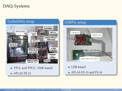
DAQ-Systems
TurboDAQ setup
TPLL and TPCC, VME based
ATLAS FE-I3
USBPix setup
USB BoardAdapter Card
Single Chip Card w/ FE-I3
USB based
ATLAS FE-I3 and FE-I4
Characterization and Testbeam Analysis of irradiated Silicon n-in-p Pixel Detectors for the ATLAS UpgradeC. Gallrapp 4 / 18
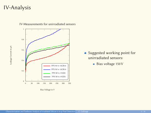
IV-Analysis
0 50 100 150 200 250 300 3500
0.2
0.4
0.6
0.8
1
Bias Voltage in V
Leak
age
Cur
rent
inµA
IV-Measurements for unirradiated sensors
PPS-W13-15GR10
PPS-W14-15GR10
PPS-W14-19GR2
PPS-W16-19GR3
Suggested working point forunirradiated sensors:
Bias voltage 150V
Characterization and Testbeam Analysis of irradiated Silicon n-in-p Pixel Detectors for the ATLAS UpgradeC. Gallrapp 5 / 18
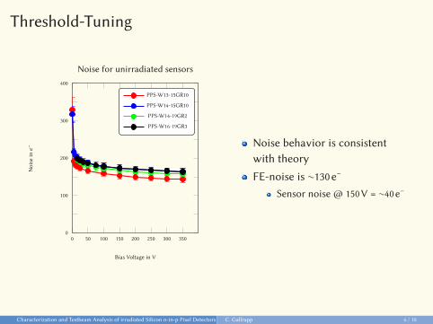
Threshold-Tuning
0 50 100 150 200 250 300 3500
100
200
300
400
Bias Voltage in V
Noi
sein
e−
Noise for unirradiated sensors
PPS-W13-15GR10
PPS-W14-15GR10
PPS-W14-19GR2
PPS-W16-19GR3
Noise behavior is consistentwith theory
FE-noise is ∼130e−
Sensor noise @ 150V = ∼40e−
Characterization and Testbeam Analysis of irradiated Silicon n-in-p Pixel Detectors for the ATLAS UpgradeC. Gallrapp 6 / 18
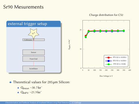
Sr90 Mesurements
external trigger setup
Sr90
Collimator
Sensor
Front End
Scintillator0 50 100 150 200 250 300 350 400
0
10
20
Bias Voltage in V
QM
PVin
ke−
Charge distribution for CS2
PPS-W13-15GR10
PPS-W14-15GR10
PPS-W14-19GR2
Theoretical values for 285µm Silicon:Qmean ∼30.7ke−
QMPV ∼21.9ke−
Characterization and Testbeam Analysis of irradiated Silicon n-in-p Pixel Detectors for the ATLAS UpgradeC. Gallrapp 7 / 18

IrradiationFinished irradiation:
CERN protons at 24GeV1 sensor at ∼6.2×10¹⁴ neq/cm2
1 SCA at ∼2×10¹⁵ neq/cm2
1 sensor at ∼2.5×10¹⁵ neq/cm2
1 SCA at ∼2.5×10¹⁵ neq/cm2
1 SCA at ∼3×10¹⁵ neq/cm2
1 sensor at ∼4.4×10¹⁵ neq/cm2
SCA cooling down
Karlsruhe protons at 25MeV1 SCA at 1×10¹⁵ neq/cm2
Ljubljana neutrons1 SCA at 1×10¹⁵ n/cm2
Upcoming irradiation:
Karlsruhe protons at 25MeV1 SCA at 3×10¹⁵ neq/cm2
1 SCA at 5×10¹⁵ neq/cm2
Ljubljana neutrons1 SCA at 3×10¹⁵ n/cm2
1 SCA at 5×10¹⁵ n/cm2
thanks to M. Glaser for the irradiation at CERNthanks to A. Dierlam and the Helmholtz Alliance for the irradiation in Karlsruhe
thanks to V. Cindro for the irradiation in Ljubljana
Characterization and Testbeam Analysis of irradiated Silicon n-in-p Pixel Detectors for the ATLAS UpgradeC. Gallrapp 8 / 18
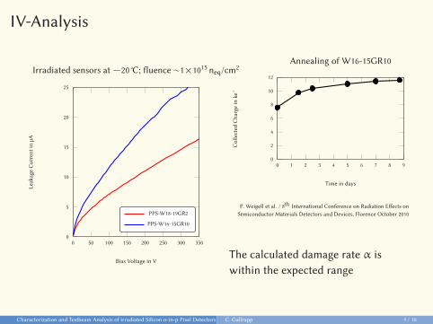
IV-Analysis
0 50 100 150 200 250 300 3500
5
10
15
20
25
Bias Voltage in V
Leak
age
Cur
rent
inµA
Irradiated sensors at −20 °C; Wuence ∼1×10¹⁵ neq/cm2
PPS-W18-19GR2
PPS-W16-15GR10
0 1 2 3 4 5 6 7 8 90
2
4
6
8
10
12
Time in days
Col
lect
edC
harg
ein
ke−
Annealing of W16-15GR10
P. Weigell et al. / 8th International Conference on Radiation EUects onSemiconductor Materials Detectors and Devices, Florence October 2010
The calculated damage rate α iswithin the expected range
Characterization and Testbeam Analysis of irradiated Silicon n-in-p Pixel Detectors for the ATLAS UpgradeC. Gallrapp 9 / 18

Noise-Analysis
0 50 100 150 200 250 300 3500
100
200
300
400
Bias Voltage
Noi
se
Noise for irradiated and unirradiated sensors
irradiated PPS-W18-19GR2
unirradiated PPS-W13-15GR10
PPS-W18-19GR2 was neutronirradiated up to 1×10¹⁵ n/cm2 inLjubljana
Noise for irradiated sensors isincreasing with higher biasvoltage
Characterization and Testbeam Analysis of irradiated Silicon n-in-p Pixel Detectors for the ATLAS UpgradeC. Gallrapp 10 / 18

Sr90 Mesurements
0 100 200 300 400 500 600 7000
5
10
15
20
25
30
35
Bias Voltage
QM
PVin
ke−
Charge distribution for CS1
irradiated PPS-W18-19GR2
unirradiated PPS-W13-15GR10
unirradiated PPS-W14-15GR10
unirradiated PPS-W14-19GR2SuXcient charge collection afterirradiation
Increasing charge collection forhigher bias voltages
∼65% of charge collection at700V bias voltage compared tounirradiated sensors
Characterization and Testbeam Analysis of irradiated Silicon n-in-p Pixel Detectors for the ATLAS UpgradeC. Gallrapp 11 / 18

Test-Beam Setup
SPS beamline (H6) with 200MeVpions
6 weeks of beam in 3 periodes
several samples from diUerentgroups
6 samples from Munich
Testbeam-Group July 2010:M. Benoit, Ch. Gallrapp, M. George, S. Grinstein, Z. Janoska, J. Jentsch, A. La Rosa,
S. Libov, D. Muenstermann, G. Piacquadio, B. Ristic, I. Rubinsky, A. Rummler,D. Sutherland, G. Troska, S. Tsiskaridze, P. Weigell, J. Weingarten, T. Wittig
Characterization and Testbeam Analysis of irradiated Silicon n-in-p Pixel Detectors for the ATLAS UpgradeC. Gallrapp 12 / 18

Test-Beam Setup
EUDET-Telescope with ∼4µmresolution
Test Beam AnalysisMatched clustersAll cluster sizes
Testbeam-Group October 2010:M. Beimforde, M. Benoit, M. Bomben, G. Calderini, Ch. Gallrapp, M. George,
S. Gibson, S. Grinstein, Z. Janoska, J. Jentzsch, O. Jinnouchi, T. Kishida, A. La Rosa,V. Libov, A. Macchiolo, G. Marchiori, D. Muenstermann, R. Nagai, G. Piacquadio,B. Ristic, I. Rubinskiy, A. Rummler, Y. Takubo, G. Troska, S. Tsiskaridze, I. Tsurin,
Y. Unno, P. Weigell, J. Weingarten, T. Wittig
Characterization and Testbeam Analysis of irradiated Silicon n-in-p Pixel Detectors for the ATLAS UpgradeC. Gallrapp 13 / 18

Test-Beam Results - Unirradiated Sensors
High eXciency for unirradiatedsensor: ε = 99.31%
Good charge collection, also inthe punch-through region wellabove threshold
EXciency map
mµLong Pixel Side/0 100 200 300 400
mµS
hort
pix
el S
ide/
0
10
20
30
40
50
90
92
94
96
98
100
Collected charge by track
mµLong Pixel Side/0 100 200 300 400
mµS
hort
pix
el S
ide/
0
10
20
30
40
50 -ke
15
20
25310×
Punch-through biasing
Preliminary TB results
Characterization and Testbeam Analysis of irradiated Silicon n-in-p Pixel Detectors for the ATLAS UpgradeC. Gallrapp 14 / 18

Test-Beam Results - Proton Irradiated Sensor 1015neq/cm2
Collected charge is inaggreement withlab-measurements
Good charge collection in thewhole sensor area
Collected charge at 500V
W16-15GR10Entries 137456Mean 1.535e+004Constant 3.557e+004MPV 1.237e+004Sigma 1146
]-Cluster charge [e0 10 20 30 40 50 60 70 80 90 100
310×
Tra
cks
0
1000
2000
3000
4000
5000
6000
W16-15GR10Entries 137456Mean 1.535e+004Constant 3.557e+004MPV 1.237e+004Sigma 1146
Collected charge by track at 500V
mµLong Pixel Side /0 50 100 150 200 250 300 350 400
mµS
ho
rt P
ixel
Sid
e /
0
5
10
15
20
25
30
35
40
45
50 ]-M
ean
Ch
arg
e [e
11
12
13
14
15
16
17
310×
Preliminary TB results
Characterization and Testbeam Analysis of irradiated Silicon n-in-p Pixel Detectors for the ATLAS UpgradeC. Gallrapp 15 / 18
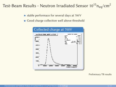
Test-Beam Results - Neutron Irradiated Sensor 1015neq/cm2
stable performace for several days at 700V
Good charge collection well above threshold
Collected charge at 700V
Preliminary TB results
Characterization and Testbeam Analysis of irradiated Silicon n-in-p Pixel Detectors for the ATLAS UpgradeC. Gallrapp 16 / 18
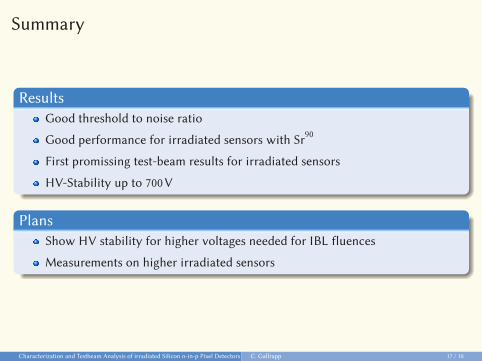
Summary
ResultsGood threshold to noise ratio
Good performance for irradiated sensors with Sr90
First promissing test-beam results for irradiated sensors
HV-Stability up to 700V
PlansShow HV stability for higher voltages needed for IBL Wuences
Measurements on higher irradiated sensors
Characterization and Testbeam Analysis of irradiated Silicon n-in-p Pixel Detectors for the ATLAS UpgradeC. Gallrapp 17 / 18

Thank you for the attention!Questions?
Characterization and Testbeam Analysis of irradiated Silicon n-in-p Pixel Detectors for the ATLAS UpgradeC. Gallrapp 18 / 18