Embed Size (px)
Citation preview
Characterization Measurements of theKATRIN Focal-Plane Detector System
Master thesisof
Agnes Seher
at the Institut for Experimental Nuclear Physics
Reviewer: Prof. Dr. Guido DrexlinSecond Reviewer: Prof. Dr. Wim de BoerAdvisor: Dr. Fabian Harms
09. November 2015 – 08. November 2016
KIT – Universität des Landes Baden-Württemberg und nationales Forschungszentrum in der Helmholtz-Gemeinschaft www.kit.edu

Messungen zur Charakterisierung desKATRIN Fokalebenen Detektor
Systems
Masterarbeitvon
Agnes Seher
am Institut für Experimentelle Kernphysik
Referent: Prof. Dr. Guido DrexlinKorreferent: Prof. Dr. Wim de BoerBetreuender Mitarbeiter: Dr. Fabian Harms
09. November 2015 – 08. November 2016
KIT – Universität des Landes Baden-Württemberg und nationales Forschungszentrum in der Helmholtz-Gemeinschaft www.kit.edu

Erklärung zur Selbstständigkeit
Ich versichere, dass ich diese Arbeit selbstständig verfasst habe und keine anderen alsdie angegebenen Quellen und Hilfsmittel benutzt habe, die wörtlich oder inhaltlichübernommenen Stellen als solche kenntlich gemacht und die Satzung des KIT zurSicherung guter wissenschaftlicher Praxis in der gültigen Fassung vom 17.05.2010beachtet habe.
Karlsruhe, den 07.11.2016,Agnes Seher
Als Ansichtsexemplar genehmigt von
Karlsruhe, den 07.11.2016,Prof. Dr. Guido Drexlin
v


Contents
1 Introduction 1
2 Neutrino Physics 32.1 Neutrinos in the Standard Model - A Historical Overview . . . . . . . 32.2 The Phenomenon of Neutrino Oscillations . . . . . . . . . . . . . . . 4
2.2.1 The Solar Neutrino Deficit . . . . . . . . . . . . . . . . . . . . 52.2.2 Theory of Neutrino Oscillation . . . . . . . . . . . . . . . . . . 62.2.3 Neutrino-Oscillation Experiments . . . . . . . . . . . . . . . . 7
2.3 Experimental Approaches to Measure the Neutrino Rest Mass . . . . 8
3 The KATRIN Experiment 133.1 The MAC-E Filter Principle . . . . . . . . . . . . . . . . . . . . . . . 133.2 Main Components . . . . . . . . . . . . . . . . . . . . . . . . . . . . 14
3.2.1 Windowless Gaseous Tritium Source . . . . . . . . . . . . . . 143.2.2 Transport Section . . . . . . . . . . . . . . . . . . . . . . . . . 163.2.3 Spectrometer and Detector Section . . . . . . . . . . . . . . . 17
3.3 Measurement Phases of the Spectrometer and Detector Section . . . . 18
4 The Focal-Plane Detector System 214.1 Magnet System . . . . . . . . . . . . . . . . . . . . . . . . . . . . . . 214.2 Post-Acceleration-Electrode . . . . . . . . . . . . . . . . . . . . . . . 214.3 Vacuum System . . . . . . . . . . . . . . . . . . . . . . . . . . . . . . 224.4 Cooling System . . . . . . . . . . . . . . . . . . . . . . . . . . . . . . 234.5 Detector Wafer . . . . . . . . . . . . . . . . . . . . . . . . . . . . . . 244.6 Readout Electronics and Data Acquisition . . . . . . . . . . . . . . . 264.7 Calibration Sources . . . . . . . . . . . . . . . . . . . . . . . . . . . . 284.8 The Veto System . . . . . . . . . . . . . . . . . . . . . . . . . . . . . 29
5 High Voltage Tests of the Post-Acceleration-Electrode of the FPD sys-tem 315.1 Discharge Phenomena . . . . . . . . . . . . . . . . . . . . . . . . . . 31
5.1.1 Field Emission . . . . . . . . . . . . . . . . . . . . . . . . . . 315.1.2 Paschen Law . . . . . . . . . . . . . . . . . . . . . . . . . . . 325.1.3 Penning Traps . . . . . . . . . . . . . . . . . . . . . . . . . . . 33
5.2 The Test Apparatus . . . . . . . . . . . . . . . . . . . . . . . . . . . 345.3 High Voltage Tests . . . . . . . . . . . . . . . . . . . . . . . . . . . . 34
5.3.1 Initial Tests . . . . . . . . . . . . . . . . . . . . . . . . . . . . 345.3.2 Pressure Dependent Tests . . . . . . . . . . . . . . . . . . . . 365.3.3 Modified System - Improvement of Sight . . . . . . . . . . . . 37
vii

5.3.4 Influence of Gas-Exposure on Conditioning . . . . . . . . . . . 375.3.5 Observations - Summarized . . . . . . . . . . . . . . . . . . . 38
5.4 Conclusion . . . . . . . . . . . . . . . . . . . . . . . . . . . . . . . . . 39
6 Commissioning and Characterization of the Detector 416.1 Spatial Resolution . . . . . . . . . . . . . . . . . . . . . . . . . . . . . 416.2 Energy resolution . . . . . . . . . . . . . . . . . . . . . . . . . . . . . 426.3 Background Measurements . . . . . . . . . . . . . . . . . . . . . . . . 44
7 Conclusions 53
Bibliography 57
1. Introduction
With the postulation of neutrinos in 1930 by W. Pauli and their experimentaldiscovery in 1956 by Reines and Cowan the problem with momentum and energyconservation in the β-decay was solved. However, 14 years later the neutrino turnedout yet again as mysterious particle when first experiments started to observe solarneutrinos. These experiments were based on a technique using radiochemicals andmeasured a flux of the electron neutrinos which differed from the predictions of theestablished standard solar model. Eventually, this was solved by the SNO experimentin 2002 which was the first of its kind that was sensitive to all neutrino flavors, andrevealed the ability of neutrinos to change their flavor. These so-called neutrino flavoroscillations directly imply a non-vanishing rest mass of at least two neutrino flavorsindicating physics beyond the standard model of particle physics. Chapter 2 givesa detailed overview of the experimental discovery of neutrinos and the theoreticaldescription of the flavor oscillations.
The KArlsruhe TRItium Neutrino (KATRIN) experiment aims to determine theeffective mass of the electron anti-neutrino. For this purpose, the energy spectrumof electrons emitted in tritium β-decay is precisely analyzed close to its endpointE0 =18.6 keV. To achieve this goal, KATRIN makes use of a high luminosity window-less gaseous tritium source from where the β-electrons are guided along magnetic fieldlines adiabatically towards a combination of two electrostatic spectrometers based onthe MAC-E filter principle. The latter act as high-pass filter such that only those withsufficient kinetic energy are able to pass their retarding potential and are counted bya focal-plane detector (FPD) system. With a sensitivity of mνe < 200meV/c2 (90%C.L.) KATRIN surpasses the sensitivity of its predecessor experiments by one orderof magnitude. The different subsystems of the KATRIN experimental beamline aredescribed in chapter 3.
The main focus of the thesis in hand is the FPD system which counts the β-electronswith a high detection efficiency. The FPD is based on a silicon PIN-diode waferwith 148 individually read-out pixels. Two superconducting solenoids provide aguiding magnetic field for the β-electrons coming from the spectrometer. Inside thesystem a post-acceleration electrode (PAE), allows to re-accelerate the β-electrons inorder to boost their kinetic energy to regions of lower intrinsic detector backgroundrate. A complex readout chain allows to monitor the signals in real time and furtherremotely operate all devices (e.g. valves, vacuum gauges, etc.). The FPD with all itssubsystems is described in chapter 4.
While designed to operate at up to +30 kV the PAE as currently installed in theFPD system experiences HV breakdowns at voltages >+10 kV. In order to improve
1
1 Introduction
the performance of this key system of the FPD several experiments were carried outin the context of the thesis in hand. These test were conducted with a separate teststand setup by the KATRIN collaboration partners at the University of Washington(UW) and are described in detail in chapter 5.
Initially the FPD system was developed and assembled at UW before it was shippedto the KATRIN experimental site at the Karlsruhe Institute of Technology (KIT)in 2011. Since then the system was commissioned, characterized, and operated injoint operation with the KATRIN main spectrometer in several extensive (SDS) mea-surement campaigns. However, even with the FPD system close to fully functioning,there is still room for improvement: During a maintenance break between two SDScampaigns, a spare wafer was installed to the system in order to characterize itsperformance. The results of these test measurements and a comparison to otherwafer is given in chapter 6 of this thesis.
2
2. Neutrino Physics
The physics Nobel Prize of 2015 was awarded to T. Kajita and A. B. McDonald forthe experimental observation of neutrino oscillations. This has drawn more attentionto neutrino physics and the physics beyond the standard model. In this chapter ashort historical overview featuring the discovery and postulation of the neutrino inthe standard model of particle physics is given in section 2.1. Observations and theoryconcerning neutrino oscillations are described in section 2.2, followed by experimentalapproaches to determine the neutrino mass in section 2.3.
2.1 Neutrinos in the Standard Model - A Historical Overview
At the end of the 19th century radioactive decay was first observed. Soon three typesof radiation were known: α-, β- and γ-radiation. While observing these decays itwas found out for the energy spectra of α- and γ-radiation to be discrete. Thoughseeming like a two-body-problem Chadwick measured a continuous energy spectrumfor β-decay in 1914 [1]. This violation of energy and momentum conservation didnot correspond to the physical knowledge which was gained so far. To resolve thisW. Pauli suggested a new particle which is additionally emitted during β-decay andelectrically neutral with spin 1/2 [2]. Instead of a two-body decay one would nowobserve a three-body decay which explains the continuous spectrum perfectly:
AZX → A
Z+1X′ + e− + νe . (2.1)
Further W. Pauli expected the mass of this particle he named “neutron” to be lessthan 1% of the proton mass.Two years later Chadwick discovered during his experiments a neutral particle in1932 [3] which was too heavy to be the one emitted out of the β-decay. It wasthe “neutron” as it is known today. Motivated by the previous work of W. Pauliand Chadwick, E. Fermi published his theory of the β-decay as a point-like weakinteraction consisting of four fermions in 1934 [4]:
n→ p + e− + νe . (2.2)
He was the first who named this particle “neutrino”. Soon after his publication H.Bethe and J. Perleis calculated the cross-section of a neutrino with a nuclei to beσ = 10−44 cm2, which corresponds to a mean free path of 1016 km in solid matter [5].This rather small cross-section let them believe it would be impossible to measure it.For two decades this assumption was right, until the “Project Poltergeist“ was buildand run by C. L. Cowen and F. Reines in 1951. The goal of this project was to
3
2 Neutrino Physics
detect the anti-neutrinos which are produced in a nuclear fission reactors in inverseβ-decays:
νe + p→ n + e+ . (2.3)
Project Poltergeist consisted of a tank filled with 200 ` water and 40 kg cadmiumchloride dissolved in it. While the protons of the water are targets for the neutri-nos the cadmium absorbs the resulting neutron which is then excited and emits aγ-photon. The free positron annihilates with an electron whereby γ photons arecreated. While the electron-positron annihilation happens fast the absorption ofthe neutron is rather slow and takes a few microseconds which allows to distinguishsignal from background, e.g. originating from the atmosphere or reactors.In 1956 the project could finally observe free electron anti-neutrinos and confirm thecalculated cross-section [6].Six years later the existence of the νµ was proven by L. M. Lederman, M. Schwartzand J. Steinberger in the Brookhaven National Laboratory using a proton beamwhich was shot on a beryllium target [7]. With the discovery of the τ lepton a ντ
neutrino was assumed and detected [8] with a similar experimental method as inBrookhaven in 2001.All these experimental researches and discoveries in the 20th century lead to the devel-opment of the standard model of particle physics as it is known today. Consisting of12 fermions, four gauge bosons and the Higgs boson it describes the strong, weak andelectromagnetic interaction as well but not fully the gravitational interaction. Thefermions are spin 1/2-particles and are divided in three generations. Each generationincludes two quarks, one with charge +2/3 and one with -1/3, as well as two leptonswith charge -1 and neutral charge. For each fermion an anti-particle with oppositesign in charge exists. The three interaction forces are carried out by the four gaugebosons: W+, W−, Z0 and γ. In 2012 the Higgs boson was discovered at the LHCwhich represents the quantum excitation of the Higgs-field, explaining why particlesare massive [9].The electric neutral neutrinos only interact weakly which processes are describedthrough the gauge bosons W+/− and Z0. The W+/− bosons only couple to left-handedfermions and right-handed anti-fermions. This leads to a maximum parity violationwhich confirms massless neutrinos. Out of Z0 boson decay the number of existingneutrino generations can be derived. It can decay in every fermion-anti-fermion pairas long as the kinematics allow it. Comparing the theoretical calculated Z0-resonancewith the one measured will reveal the number of neutrino generations which wasanalyzed to be Nν = 2.984 ± 0.008 [10].The standard model as it is established today, describes most known physics well.However, there are still physical observations which are not explainable with it: theexpansion of the universe, dark matter particles and neutrino oscillations.
2.2 The Phenomenon of Neutrino Oscillations
The idea of neutrino oscillation was first proposed by B. Pontecorvo in 1957 [11]. Theinitial theory described an oscillation between neutrino and anti-neutrino, however,an improved version of the neutrino oscillation theory was established describing anoscillation between the three neutrino flavors in the 1970’s . In the following thediscoveries, theory, and experiments concerning neutrino oscillations are described.
4
2.2 The Phenomenon of Neutrino Oscillations
13N
15O
17F
7Be ±10.5%
pp ±1%
8B±16%
hep±16%
7Be±10.5%
pep ±2%
Bahcall-Serenelli 2005
Neutrino spectrum (±1σ)
Neutrino energy (MeV)0.1 1 10
102
103
104
105
106
107
108
109
1010
1011
1012
Flu
x(c
m-2
s-1)
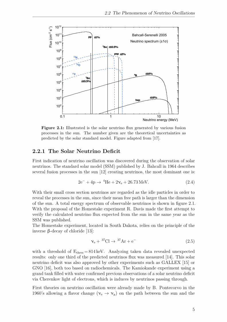
Figure 2.1: Illustrated is the solar neutrino flux generated by various fusionprocesses in the sun. The number given are the theoretical uncertainties aspredicted by the solar standard model. Figure adapted from [17].
2.2.1 The Solar Neutrino DeficitFirst indication of neutrino oscillation was discovered during the observation of solarneutrinos. The standard solar model (SSM) published by J. Bahcall in 1964 describesseveral fusion processes in the sun [12] creating neutrinos, the most dominant one is:
2e− + 4p→ 4He + 2νe + 26.73MeV. (2.4)
With their small cross section neutrinos are regarded as the idle particles in order toreveal the processes in the sun, since their mean free path is larger than the dimensionof the sun. A total energy spectrum of observable neutrinos is shown in figure 2.1.With the proposal of the Homestake experiment R. Davis made the first attempt toverify the calculated neutrino flux expected from the sun in the same year as theSSM was published.The Homestake experiment, located in South Dakota, relies on the principle of theinverse β-decay of chloride [13]:
νe + 37Cl→ 37Ar + e− (2.5)
with a threshold of Ethres =814 keV. Analyzing taken data revealed unexpectedresults: only one third of the predicted neutrinos flux was measured [14]. This solarneutrino deficit was also approved by other experiments such as GALLEX [15] orGNO [16], both too based on radiochemicals. The Kamiokande experiment using agrand tank filled with water confirmed previous observations of a solar neutrino deficitvia Cherenkov light of electrons, which is induces by neutrinos passing through.
First theories on neutrino oscillation were already made by B. Pontecorvo in the1960’s allowing a flavor change (νe → νµ) on the path between the sun and the
5
2 Neutrino Physics
detector [11, 18]. Previous mentioned experiments were only sensitive to electronneutrinos, hence, leaving the solar neutrino problem unsolved.Finally, the Sudbury Neutrino Observatory (SNO) experiment, located in Ontario,Canada was able to verify the solar neutrino flux [19]. Using a tank of 1000 t heavywater it was the first experiment which was not only sensitive to electron neutrinosvia the charged current (CC) but also to muon and tauon neutrinos via neutralcurrent (NC) and elastic scattering (ES) processes:
νe + d→ p + p + e− (CC), (2.6)νx + d→ p + n + νx (NC), (2.7)νx + e− → νx + e− (ES), (2.8)
with x= e,µ,τ. Results showed a similar electron neutrino flux as measured byprevious experiments. However, the determined flux of all neutrino flavors verifiedthe proposed flux by the SSM [20].
2.2.2 Theory of Neutrino OscillationPontecorvo was the first who predicted the possibility of the neutrino flavors notbeing the eigenstates of the particles itself. This observations were based on of kaonoscillations where particle and anti-particle transform into each other (K0 ↔ K0)due to quark flavor oscillations [21]. At a later point, this theory was transfered toneutrino flavor oscillations [18, 22].
Analogous to the Cabibbo-Kobayashi-Maskawa (CKM) matrix for the mixing ofquark flavors based on different weak- and mass eigenstates a matrix for the mixingof neutrino flavors was found. It is based on non-identical flavor- |να〉 and mass- |νi〉eigenstates (α=e,ν,τ and i= 1,2,3). Both are connected via a 3×3 mixing matrix U:
|να〉 =∑
iUα,i |νi〉 . (2.9)
The matrix was introduced by Maki, Nagakawa and Sakata (PMNS-matrix) in 1962and is adapted from previous research of Pontecorvo. It describes the flavor mixingbased on three mixing angles Θ23, Θ13, Θ12 and a CP violating phase δ used forparametrization:1 0 0
0 c23 s230 −s23 c23
· c13 0 s13e
−iδ
0 1 0−s13e
−iδ 0 c13
· c12 s12 0−s12 c12 0
0 0 1
(2.10)
with sij = sin Θij and cij = cos Θij whereby the matrix itself is split into three partsaccording to the mixing angles. Neutrinos produced at a time t= 0 are in a pure flavoreigenstate. As the neutrino propagates on one-dimensional path the time-evolutionof the mass eigenstate is given by a plane wave (in the following natural units areused):
|νi(t)〉 = e−iEit |νi〉 (2.11)Hence, a flavor eigenstate at a later time t> 0 is described by:
|να(t)〉 =∑
iUα,ie
−iEit |νi〉 =∑i,β
Uα,iU∗β,ie−iEit |νβ〉 . (2.12)
6
2.2 The Phenomenon of Neutrino Oscillations
The probability for a neutrino of the flavor να to transform into a flavor νβ is thengiven by:
Pνα→νβ(t) = | 〈νβ(t)|να(t)〉 |2 =
∑i,j
Uα,iU∗β,iU∗α,jUβ,je−i(Ei−Ej)t. (2.13)
For ultra-relativistic neutrinos (pimi and E≈ pi) this equation 2.13 can be simpli-fied to:
Pνα→νβ(L/E) =
∑i,j
Uα,iU∗β,iU∗α,jUβ,je−i
∆m2ijL
2E . (2.14)
The baseline length L hereby represents the distance between source and detectorand E the energy of the neutrino. ∆m2
i,j holds information about the difference of thesquared masses of the neutrino mass eigenstates. This equation allows to estimatethe supposed distance between the source and the detector depending on neutrinoenergy, mass differences and mixing angles in order to measure the appearance ordisappearance of neutrino flavors.
2.2.3 Neutrino-Oscillation Experiments
To observe the neutrino flux and oscillation in general the experiments can bedivided into two different techniques. First experiments were based on radiochemicaltechniques as used in the Homestake experiment by Davis which makes use of theinverse β-decay. An improvement of this experiment type was achieved by GALLEXor GNO due to the lower energy threshold of the transformation of gallium togermanium. On the other hand, the technique firstly used by SNO depends on a largetank filled with heavy water. This enables the observation of all three neutrino flavorsin real-time via Cherenkov light and gives further insight on neutrino oscillation forenergies larger than 1.9MeV. An aspect which has to be taken into account whenmeasuring the Θ12 and ∆m2
12 is the influence of matter on the νe due to the presenceof electrons in matter. This is the so-called MSW-effect introduced in the 1970’s and1980’s [23]. The different mixing angles can be determined by measuring neutrinosof various sources.
Cosmic rays with energies in the GeV range induce a large number of particles withtwice as much muon neutrinos than electron neutrinos both too with energies in theGeV range. The Super-Kamiokande experiment located in Japan makes use of alarge tank filled with 50 kt ultra-pure water and 11 000 photomultipliers attached onthe tank walls. This setup allows to investigate the up-down symmetry or asymmetryof νµ and µe as a function of distance through matter via Cherenkov light. Thegreat advantage of such a measurement principle is the real-time distinguish abilityfor νµ and µe. Results show a νµ deficit as an up-down asymmetry regarding theatmospheric neutrino flux. Furthermore, with a measurable ντ flux this deficit wasconfirmed. With the Super-Kamiokande and Ice-Cube [24, 25] experiment the Θ23mixing angle as well as the squared mass difference ∆m2
23 are well studied parametersof the neutrino mixing.
Another source of a large neutrino flux are nuclear power plants with Φνe = 2·1020 s−1.Reactor neutrinos have energies of a few MeV. With a baseline length of 1 km to2 km detectors are then able to measure the scale of Θ13 and ∆m2
13. Experiments likeDaya Bay (China) and Double Chooz (France) make use of a combination of two
7
2 Neutrino Physics
m2 m2
m21
0
? ?
solar Δm212
atmosphericΔm2
32
atmosphericΔm2
32
m22
m23
m23
m21
m22
solar Δm212
νe
νμντ
0
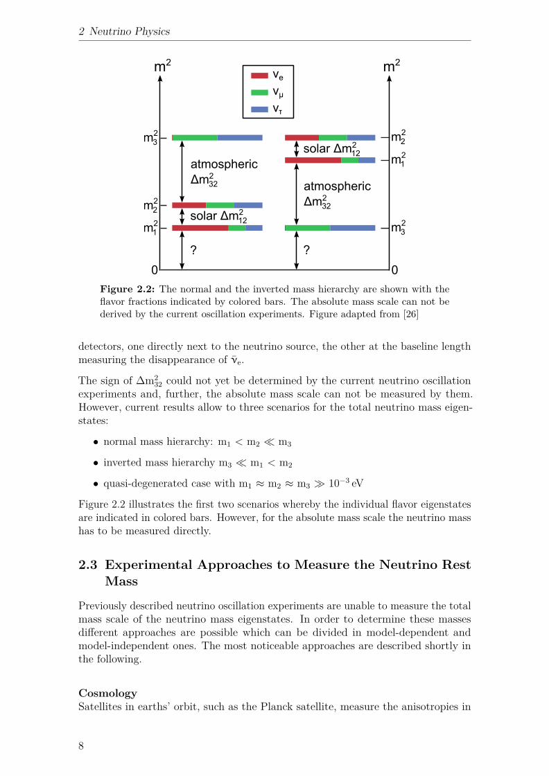
Figure 2.2: The normal and the inverted mass hierarchy are shown with theflavor fractions indicated by colored bars. The absolute mass scale can not bederived by the current oscillation experiments. Figure adapted from [26]
detectors, one directly next to the neutrino source, the other at the baseline lengthmeasuring the disappearance of νe.
The sign of ∆m232 could not yet be determined by the current neutrino oscillation
experiments and, further, the absolute mass scale can not be measured by them.However, current results allow to three scenarios for the total neutrino mass eigen-states:
• normal mass hierarchy: m1 < m2 m3
• inverted mass hierarchy m3 m1 < m2
• quasi-degenerated case with m1 ≈ m2 ≈ m3 10−3 eV
Figure 2.2 illustrates the first two scenarios whereby the individual flavor eigenstatesare indicated in colored bars. However, for the absolute mass scale the neutrino masshas to be measured directly.
2.3 Experimental Approaches to Measure the Neutrino RestMass
Previously described neutrino oscillation experiments are unable to measure the totalmass scale of the neutrino mass eigenstates. In order to determine these massesdifferent approaches are possible which can be divided in model-dependent andmodel-independent ones. The most noticeable approaches are described shortly inthe following.
CosmologySatellites in earths’ orbit, such as the Planck satellite, measure the anisotropies in
8
2.3 Experimental Approaches to Measure the Neutrino Rest Mass
the temperature of the cosmic microwave background (CMB). The CMB exists dueto the expansion of the universe which forced the decoupling of photons from matterabout 380 000 years after the Big Bang. According to this, the decoupling of neutrinosfrom matter leave a cosmic neutrino background. These so-called relic neutrinoshave very low energies and in combination with their small cross section experimentswere not yet able to detect them. The cosmological model estimates a density Ων forthe relic neutrinos of 336 cm−3. Comparing this to the total energy density of theuniverse Ωtot it yields to a total mass for all three neutrino mass eigenstates of:∑
kmk = 93Ωνh2eV, (2.15)
whereby h is the dimensionless Hubble parameter. With latest achieved results amodel-dependent upper limit for all neutrino mass eigenstates is derived to [27]:∑
kmk ≤ 0.23 eV. (2.16)
Double β-DecayNuclei with an even mass number can have an equal number of neutrons and protonsin even-even or odd-odd configuration. For some of these nuclei the single β-decay isenergetically forbidden and the rare double β-decay (2νββ) becomes observable. Inthis decay two protons or two neutron decay simultaneously:
2n→ 2p + 2e− + 2νe (2.17)2p→ 2n + 2e+ + 2νe. (2.18)
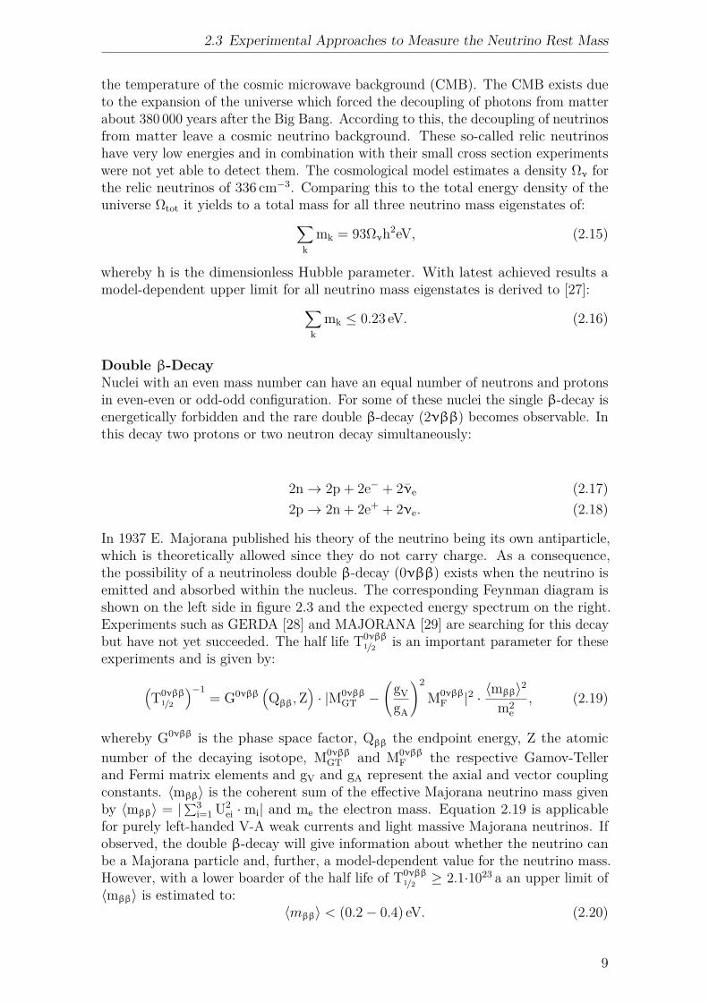
In 1937 E. Majorana published his theory of the neutrino being its own antiparticle,which is theoretically allowed since they do not carry charge. As a consequence,the possibility of a neutrinoless double β-decay (0νββ) exists when the neutrino isemitted and absorbed within the nucleus. The corresponding Feynman diagram isshown on the left side in figure 2.3 and the expected energy spectrum on the right.Experiments such as GERDA [28] and MAJORANA [29] are searching for this decaybut have not yet succeeded. The half life T0νββ
1/2 is an important parameter for theseexperiments and is given by:
(T0νββ
1/2
)−1= G0νββ
(Qββ,Z
)· |M0νββ
GT −(gVgA
)2
M0νββF |2 · 〈mββ〉2
m2e
, (2.19)
whereby G0νββ is the phase space factor, Qββ the endpoint energy, Z the atomicnumber of the decaying isotope, M0νββ
GT and M0νββF the respective Gamov-Teller
and Fermi matrix elements and gV and gA represent the axial and vector couplingconstants. 〈mββ〉 is the coherent sum of the effective Majorana neutrino mass givenby 〈mββ〉 = |∑3
i=1 U2ei ·mi| and me the electron mass. Equation 2.19 is applicable
for purely left-handed V-A weak currents and light massive Majorana neutrinos. Ifobserved, the double β-decay will give information about whether the neutrino canbe a Majorana particle and, further, a model-dependent value for the neutrino mass.However, with a lower boarder of the half life of T0νββ
1/2 ≥ 2.1·1023 a an upper limit of〈mββ〉 is estimated to:
〈mββ〉 < (0.2− 0.4) eV. (2.20)
9
2 Neutrino Physics
W-
W-
udu
udd
udd
du
u
e-
e-
p
p
n
n
νm
2.0
1.5
1.0
0.5
00 0.2 0.4 0.6 0.8 1.0
ββ (0ν)
ββ (2ν)
dN/d
(E/E
0)
E/E0
Figure 2.3: Double β-decay: On the left side the Feynman diagram of theneutrinoless double β-decay is shown. Due to the exchange of virtual neutrinosonly two electrons are emitted by the nucleus. On the right side the energyspectrum is displayed. The spectrum is scaled by a factor 1 (0.2) for the 2νββ(0νββ) decay. Figures adapted from [30, 31].
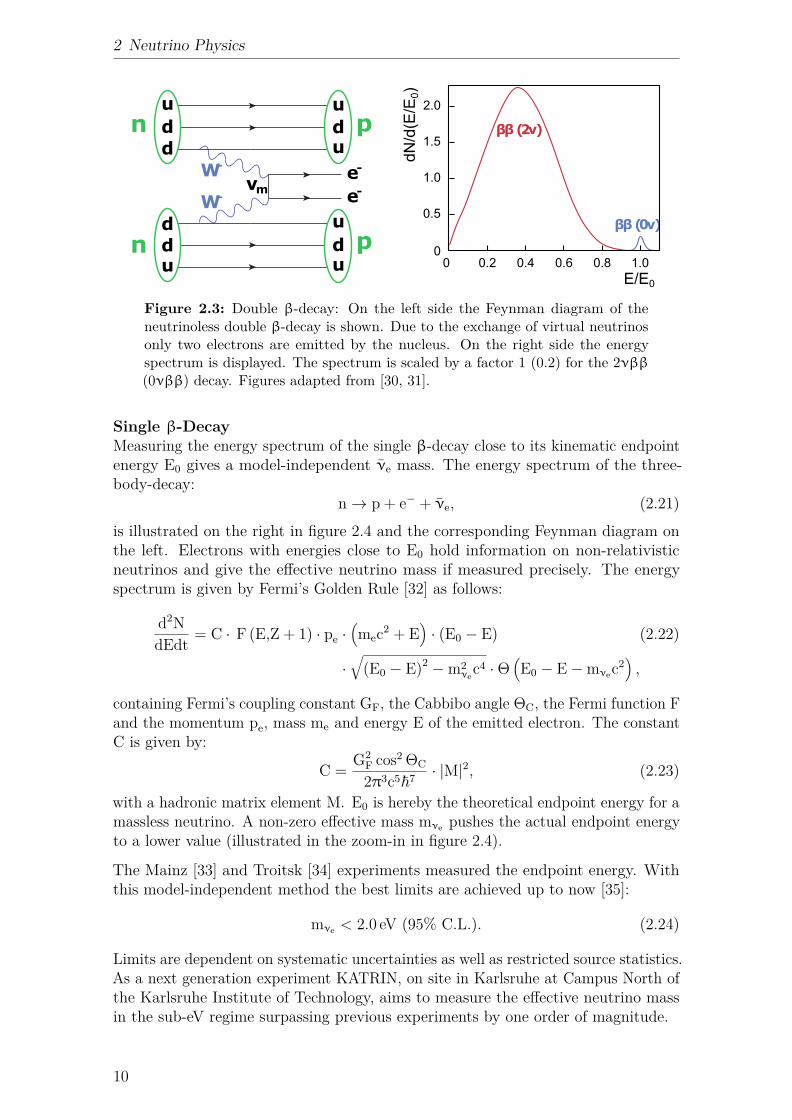
Single β-DecayMeasuring the energy spectrum of the single β-decay close to its kinematic endpointenergy E0 gives a model-independent νe mass. The energy spectrum of the three-body-decay:
n→ p + e− + νe, (2.21)is illustrated on the right in figure 2.4 and the corresponding Feynman diagram onthe left. Electrons with energies close to E0 hold information on non-relativisticneutrinos and give the effective neutrino mass if measured precisely. The energyspectrum is given by Fermi’s Golden Rule [32] as follows:
d2NdEdt = C · F (E,Z + 1) · pe ·
(mec2 + E
)· (E0 − E) (2.22)
·√
(E0 − E)2 −m2νec4 ·Θ
(E0 − E−mνec2
),
containing Fermi’s coupling constant GF, the Cabbibo angle ΘC, the Fermi function Fand the momentum pe, mass me and energy E of the emitted electron. The constantC is given by:
C = G2F cos2 ΘC
2π3c5~7 · |M|2, (2.23)
with a hadronic matrix element M. E0 is hereby the theoretical endpoint energy for amassless neutrino. A non-zero effective mass mνe pushes the actual endpoint energyto a lower value (illustrated in the zoom-in in figure 2.4).
The Mainz [33] and Troitsk [34] experiments measured the endpoint energy. Withthis model-independent method the best limits are achieved up to now [35]:
mνe < 2.0 eV (95% C.L.). (2.24)
Limits are dependent on systematic uncertainties as well as restricted source statistics.As a next generation experiment KATRIN, on site in Karlsruhe at Campus North ofthe Karlsruhe Institute of Technology, aims to measure the effective neutrino massin the sub-eV regime surpassing previous experiments by one order of magnitude.
10
2.3 Experimental Approaches to Measure the Neutrino Rest Mass
W-
udu
udd
e-
n
νe
2.0
1.5
1.0
0.5
00 0.2 0.4 0.6 0.8 1.0
0-1-2-3
mν=0mν>0
E-E0 (eV)
dN/d
(E/E
0)
E/E0
-
p
Figure 2.4: Single β-decay: On the left side the Feynman diagram is displayed.A neutron transforms into a proton while emitting a W− boson which eventuallydecays into an electron and a neutrino. The right side shows the correspondingenergy spectrum of the single β-decay. A zoom-in shows the endpoint of theenergy spectrum with a neutrino mass of 1 eV (blue dashed line) in comparisonto a vanishing neutrino mass (solid red line). Figures adapted from [30].
11

3. The KATRIN Experiment
The Karlsruhe Tritium Neutrino experiment (KATRIN), located in Karlsruhe,Germany aims to determinate the mass of the electron anti-neutrino through precisemeasurement of the kinematics of the tritium β-decay. With a sensitivity of 200meV/c2 it will improve the current neutrino mass sensitivity given by previousexperiments by one order of magnitude. The KATRIN collaboration consists ofseveral institutes and universities spread all over the world with significant contributionfrom Germany and USA.
In this chapter the KATRIN measurement principle using a MAC-E filter (section3.1) as well as the main components (section 3.2) and the measurement phases ofthe spectrometer and detector section (SDS) system (section 3.3) are described.
More details on the KATRIN experiment and its components are given in the [36].
3.1 The MAC-E Filter PrincipleTo determine the mass of the neutrino the KATRIN experiment will investigate thetritium β-spectrum close to the endpoint energy E0 = 18.6 keV with high precision.Therefore KATRIN utilizes the measurement principle of a Magnetic AdiabaticCollimation combined with an Electrostatic (MAC-E) filter [37]. This principlecombines electric and magnetic fields, shown in figure 3.1. The β-decay electronsare guided by the magnetic field, provided by superconducting solenoids along thebeamline, adiabatically through a spectrometer towards the detector. The electricfield, parallel to the magnetic field, is provided by applying (negative) high voltageon the spectrometer vessel forming a potential barrier U0 for incoming electrons. Toovercome this barrier the electrons require a longitudinal energy of E|| ≥ e·U0. Thepotential U0 can be varied in order to scan the energy spectrum of the electrons inan integral way. In β-decay electrons are emitted isotropically and, hence, posses atransverse energy component E⊥ as well. In order to use most of the source luminosityand to increase statistics at the endpoint E0 of the energy spectrum while at thesame time measuring the full kinetic energy of the electrons, the transverse energyis transformed into longitudinal energy. This is implemented through varying themagnetic field strength along the electron trajectories within the spectrometer. Tofulfill the following relation of the magnetic momentum µ of the electrons
µ = E⊥B = const (3.1)
the magnetic field has to vary slow enough (adiabatically). This equations concludesthat the transverse energy component is minimal when the magnetic field is at its
13
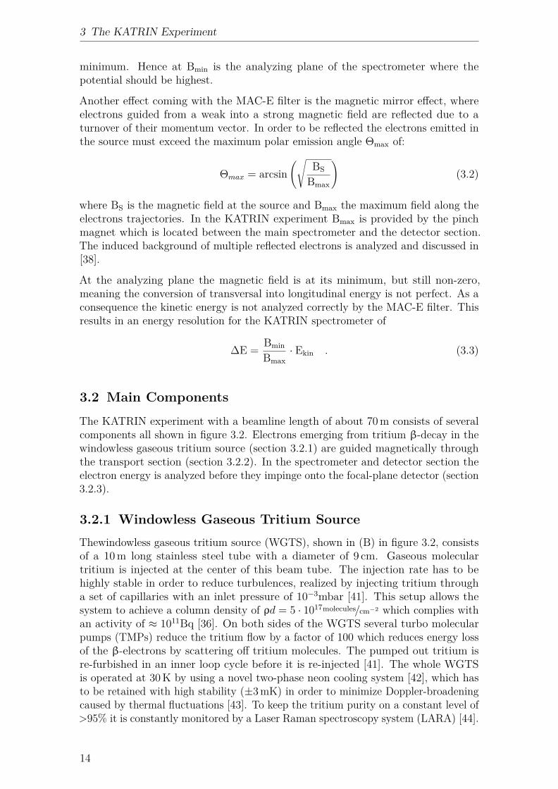
3 The KATRIN Experiment
minimum. Hence at Bmin is the analyzing plane of the spectrometer where thepotential should be highest.
Another effect coming with the MAC-E filter is the magnetic mirror effect, whereelectrons guided from a weak into a strong magnetic field are reflected due to aturnover of their momentum vector. In order to be reflected the electrons emitted inthe source must exceed the maximum polar emission angle Θmax of:
Θmax = arcsin(√
BS
Bmax
)(3.2)
where BS is the magnetic field at the source and Bmax the maximum field along theelectrons trajectories. In the KATRIN experiment Bmax is provided by the pinchmagnet which is located between the main spectrometer and the detector section.The induced background of multiple reflected electrons is analyzed and discussed in[38].
At the analyzing plane the magnetic field is at its minimum, but still non-zero,meaning the conversion of transversal into longitudinal energy is not perfect. As aconsequence the kinetic energy is not analyzed correctly by the MAC-E filter. Thisresults in an energy resolution for the KATRIN spectrometer of
∆E = Bmin
Bmax· Ekin . (3.3)
3.2 Main Components
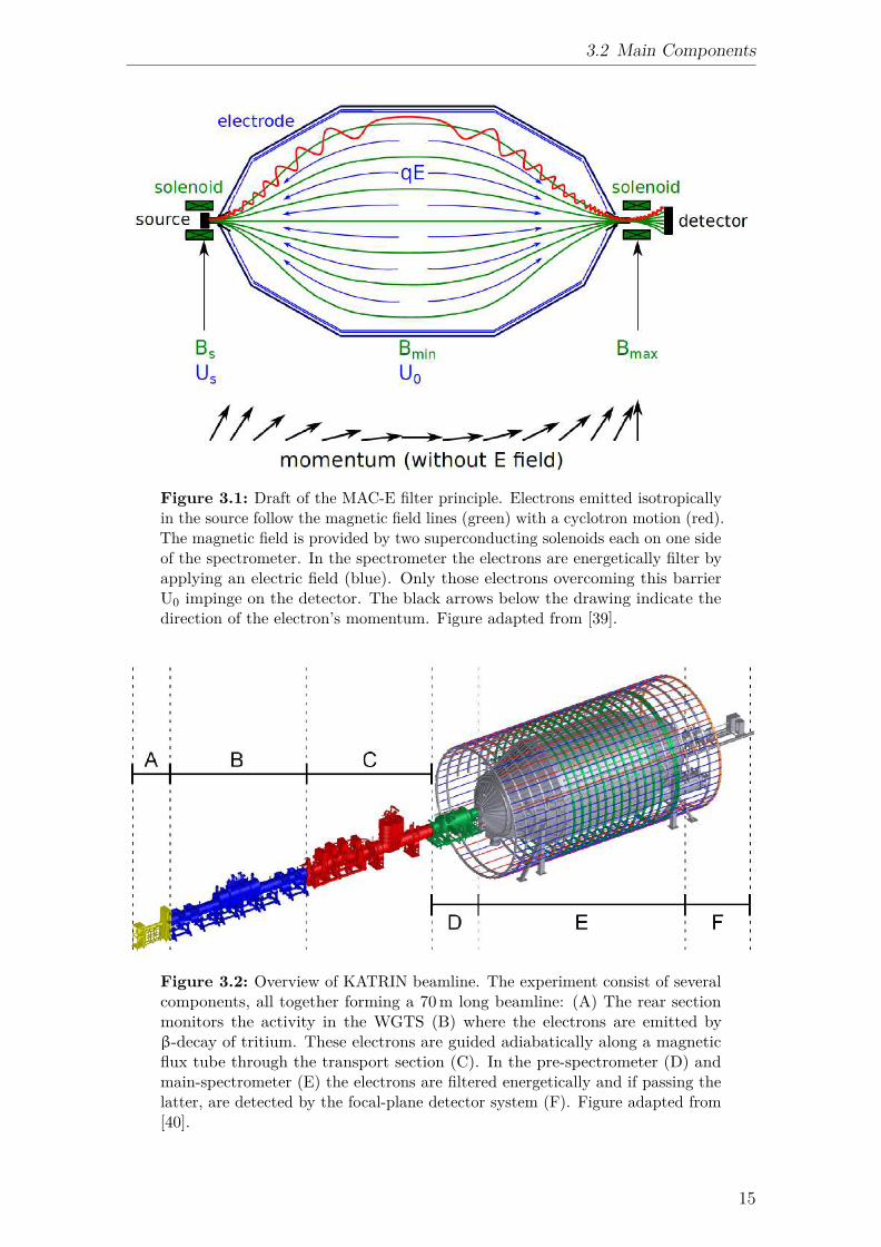
The KATRIN experiment with a beamline length of about 70m consists of severalcomponents all shown in figure 3.2. Electrons emerging from tritium β-decay in thewindowless gaseous tritium source (section 3.2.1) are guided magnetically throughthe transport section (section 3.2.2). In the spectrometer and detector section theelectron energy is analyzed before they impinge onto the focal-plane detector (section3.2.3).
3.2.1 Windowless Gaseous Tritium SourceThewindowless gaseous tritium source (WGTS), shown in (B) in figure 3.2, consistsof a 10m long stainless steel tube with a diameter of 9 cm. Gaseous moleculartritium is injected at the center of this beam tube. The injection rate has to behighly stable in order to reduce turbulences, realized by injecting tritium througha set of capillaries with an inlet pressure of 10−3mbar [41]. This setup allows thesystem to achieve a column density of ρd = 5 · 1017molecules/cm−2 which complies withan activity of ≈ 1011Bq [36]. On both sides of the WGTS several turbo molecularpumps (TMPs) reduce the tritium flow by a factor of 100 which reduces energy lossof the β-electrons by scattering off tritium molecules. The pumped out tritium isre-furbished in an inner loop cycle before it is re-injected [41]. The whole WGTSis operated at 30K by using a novel two-phase neon cooling system [42], which hasto be retained with high stability (±3mK) in order to minimize Doppler-broadeningcaused by thermal fluctuations [43]. To keep the tritium purity on a constant level of>95% it is constantly monitored by a Laser Raman spectroscopy system (LARA) [44].
14
3.2 Main Components
Figure 3.1: Draft of the MAC-E filter principle. Electrons emitted isotropicallyin the source follow the magnetic field lines (green) with a cyclotron motion (red).The magnetic field is provided by two superconducting solenoids each on one sideof the spectrometer. In the spectrometer the electrons are energetically filter byapplying an electric field (blue). Only those electrons overcoming this barrierU0 impinge on the detector. The black arrows below the drawing indicate thedirection of the electron’s momentum. Figure adapted from [39].
Figure 3.2: Overview of KATRIN beamline. The experiment consist of severalcomponents, all together forming a 70m long beamline: (A) The rear sectionmonitors the activity in the WGTS (B) where the electrons are emitted byβ-decay of tritium. These electrons are guided adiabatically along a magneticflux tube through the transport section (C). In the pre-spectrometer (D) andmain-spectrometer (E) the electrons are filtered energetically and if passing thelatter, are detected by the focal-plane detector system (F). Figure adapted from[40].
15
3 The KATRIN Experiment
The β-electrons are adiabatically guided in a magnetic field of BS = 3.6T providedby several superconducting solenoids surrounding the beam tube. Only a small partof the isotropically emitted β electrons contribute to the endpoint E0 of the energyspectrum. To increase the number of analyzable electrons the β-decay is withina magnetic field, allowing to analyze all β-electrons with a starting polar angle of<Θmax.
Mounted on the upstream side of the WGTS is the rear section. Its task is to controland monitor the activity within the WGTS: the electric potential of the tritiumplasma, and the column density of the tritium gas.
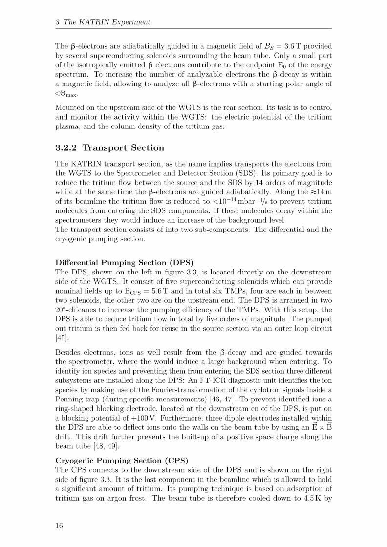
3.2.2 Transport SectionThe KATRIN transport section, as the name implies transports the electrons fromthe WGTS to the Spectrometer and Detector Section (SDS). Its primary goal is toreduce the tritium flow between the source and the SDS by 14 orders of magnitudewhile at the same time the β-electrons are guided adiabatically. Along the ≈14mof its beamline the tritium flow is reduced to <10−14 mbar · l/s to prevent tritiummolecules from entering the SDS components. If these molecules decay within thespectrometers they would induce an increase of the background level.The transport section consists of into two sub-components: The differential and thecryogenic pumping section.
Differential Pumping Section (DPS)The DPS, shown on the left in figure 3.3, is located directly on the downstreamside of the WGTS. It consist of five superconducting solenoids which can providenominal fields up to BCPS = 5.6T and in total six TMPs, four are each in betweentwo solenoids, the other two are on the upstream end. The DPS is arranged in two20-chicanes to increase the pumping efficiency of the TMPs. With this setup, theDPS is able to reduce tritium flow in total by five orders of magnitude. The pumpedout tritium is then fed back for reuse in the source section via an outer loop circuit[45].
Besides electrons, ions as well result from the β-decay and are guided towardsthe spectrometer, where the would induce a large background when entering. Toidentify ion species and preventing them from entering the SDS section three differentsubsystems are installed along the DPS: An FT-ICR diagnostic unit identifies the ionspecies by making use of the Fourier-transformation of the cyclotron signals inside aPenning trap (during specific measurements) [46, 47]. To prevent identified ions aring-shaped blocking electrode, located at the downstream en of the DPS, is put ona blocking potential of +100V. Furthermore, three dipole electrodes installed withinthe DPS are able to deflect ions onto the walls on the beam tube by using an ~E× ~Bdrift. This drift further prevents the built-up of a positive space charge along thebeam tube [48, 49].
Cryogenic Pumping Section (CPS)The CPS connects to the downstream side of the DPS and is shown on the rightside of figure 3.3. It is the last component in the beamline which is allowed to holda significant amount of tritium. Its pumping technique is based on adsorption oftritium gas on argon frost. The beam tube is therefore cooled down to 4.5K by
16
3.2 Main Components
Figure 3.3: Components of the KATRIN transport section.Left: The Differential Pumping Section (DPS). It consists of five superconductingsolenoids (dark cyan) and six turbo molecular pumps, four in between the magnets(cyan) and two on the upstream end (red). These parts are aligned along two 20chicanes reducing the tritium flow in total by five orders of magnitude. Figureadapted from [50].Right: The Cryogenic Pumping Section (CPS). Consisting of seven superconduct-ing solenoids aligned in two 15 chicanes the CPS uses argon frost to accumulatetritium on the inner surface of the beam tube via cryosorption (red). With thismethod the tritium flow is further reduced by seven orders of magnitude. Figureadapted from ([39]).
liquid helium in order to maintain an argon frost layer on its inner surface. The CPShas to be regenerated every 60 days and the accumulated tritium is pumped out ofthe system and fed back into the tritium cycle. For regeneration the beam tube iswarmed up to 100K and flushed with warm helium gas. Afterwards the argon frostlayer is renewed. The trapping efficiency of tritium is increased by arranging thebeam tube in two 15-chicanes so the tritium molecules have no direct line of sightto the spectrometers [51]. Overall this reduces the tritium flow by seven orders ofmagnitude.For guiding the β-electrons to the SDS section seven solenoids are aligned along thebeamline. Furthermore, the beamline is of the CPS is equipped with a condensedkrypton source and a beam monitoring detector which can be moved in and out ofthe beamline without breaking the vacuum [52].
3.2.3 Spectrometer and Detector Section
On the downstream side of the transport section the tritium-free spectrometer and de-tector section (SDS) is located. It consists of two electrostatic retarding spectrometersusing the MAC-E filter principle described in section 3.1 and a Focal-Plane-Detector(FPD) system described in detail in section 4. The efficient reduction of the tritiumflow in the transport section results in a low background generated by β-decays oftritiated particles. For further minimization of background rate the spectrometersoperate at pressures in the ultra high vacuum (UHV) regime at about 10−11 mbar inorder to avoid background induced by scattering effects of β-electrons with residualgas.
17
3 The KATRIN Experiment
Pre-Spectrometer
The pre-spectrometer (PS), shown (D) in figure 3.2, is a vacuum vessel with 3.4mlength and 1.7m diameter [36]. The magnetic field for its MAC-E filter is providedby two superconducting solenoids PS1 and PS2, one on each side of the spectrometer.Operating the solenoids at a nominal field of 4.5T results in an energy resolutionof ∆E ≈70 eV for electrons with an energy of E0 = 18.6 keV. The PS can be usedas a pre-filter for low-energy electrons of the tritium β-decay and, thus, reduce theelectron flux entering the main-spectrometer by seven orders of magnitude. A reducedelectron flux further reduces the background induced by scattering of β-electrons offresidual gas and is advantageous for the detector which cannot handle rates largerthan 106e−/s. One issue which arises and has to be taken into account when operatingthe PS at high voltages is the creation of a large penning trap [53] between the pre-and main-spectrometer. This has to be "neutralized" in order to prevent a majorbackground.
Main-Spectrometer
The main spectrometer (MS), shown in (E) figure 3.2, is a large stainless steelvessel 23m in length with a maximal diameter of 10m. The two solenoids providingthe magnetic field for its MAC-E filter are the PS2 on its upstream side, which itshares with the pre-spectrometer, and the pinch magnet (PCH) on the downstreamside which is part of the detector system. The PCH magnet provides the strongestmagnetic field of BP CH = 6T in the whole KATRIN beamline. With a minimalmagnetic field of Bmin = 0.3mT in the analyzing plane of the MS this results in anenergy resolution of ∆E= 0.93 eV at an electron energy of E0 = 18.6 keV [36]. Forfine-tuning the magnetic field inside the MS its vessel is surrounded by a system ofair-coils [54]. To fine-shape the electric field inside the spectrometer a two-layer wireelectrode is installed on its inner surface.
Another advantage of these wire electrode is it keeps the low-energy electrons emittedfrom the inside surface of the vessel from entering the sensitive volume of spectrom-eter. The retarding potential of this spectrometer is variable and, hence, able toscan the energy spectrum close to the endpoint E0 (so-called tritium scanning mode,scans an energy interval of E0 - 30 eV to E0 + 5 eV).
Focal-Plane Detector
The last component of the KATRIN beamline is the Focal-Plane Detector (FPD). Itis located on the downstream side of the main-spectrometer and counts the electronswhich pass the MAC-E filter. Only a few signal electrons per second are expectedduring measurements with tritium, but for calibration measurements the detectorhas to be able to measure rates of a few kHz. The whole FPD apparatus is describedin more detail in chapter 4.
3.3 Measurement Phases of the Spectrometer and DetectorSection
Two SDS measurement phases were already performed with FPD system and themain-spectrometer in tandem operation. The main goal of these campaigns was to
18
3.3 Measurement Phases of the Spectrometer and Detector Section
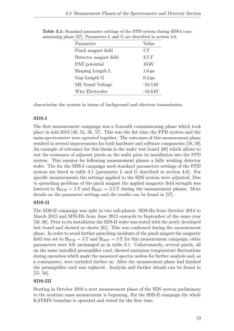
Table 3.1: Standard parameter settings of the FPD system during SDS-I com-missioning phase [57]. Parameters L and G are described in section 4.6.
Parameter ValuePinch magnet field 5TDetector magnet field 3.5TPAE potential 10 kVShaping Length L 1.6µsGap Length G 0.2µsMS Vessel Voltage -18.5 kVWire Electrodes -18.6 kV
characterize the system in terms of background and electron transmission.
SDS-IThe first measurement campaign was a 3-month commissioning phase which tookplace in mid 2013 [40, 55, 56, 57]. This was the fist time the FPD system and themain-spectrometer were operated together. The outcomes of this measurement phaseresulted in several improvements for both hardware and software components [58, 59].An example of relevance for this thesis is the wafer test board [60] which allows totest the resistance of adjacent pixels on the wafer prior its installation into the FPDsystem. This ensures for following measurement phases a fully working detectorwafer. The for the SDS-I campaign used standard parameters settings of the FPDsystem are listed in table 3.1 (parameter L and G described in section 4.6). Forspecific measurements the settings applied to the SDS system were adjusted. Dueto quenching problems of the pinch magnet the applied magnetic field strength waslowered to BPCH = 5T and BDET = 3.5T during the measurement phases. Moredetails on the parameter settings and the results can be found in [57].SDS-IIThe SDS-II campaign was split in two sub-phases: SDS-IIa from October 2014 toMarch 2015 and SDS-IIb from June 2015 onwards to September of the same year[50, 38]. Prior to its installation the SDS-II wafer was tested with the newly developedtest board and showed no shorts [61]. This was confirmed during the measurementphase. In order to avoid further quenching incidents of the pinch magnet the magneticfield was set to BPCH = 5T and BDET = 3T for this measurement campaign, otherparameters were left unchanged as in table 3.1. Unfortunately, several pixels, allon the same installed preamplifier card, showed enormous temperature fluctuationsduring operation which made the measured spectra useless for further analysis and, asa consequence, were excluded further on. After the measurement phase had finishedthe preamplifier card was replaced. Analysis and further details can be found in[55, 50].SDS-IIIStarting in October 2016 a next measurement phase of the SDS system preliminaryto the neutrino mass measurement is beginning. For the SDS-II campaign the wholeKATRIN beamline is operated and tested for the first time.
19

4. The Focal-Plane DetectorSystem
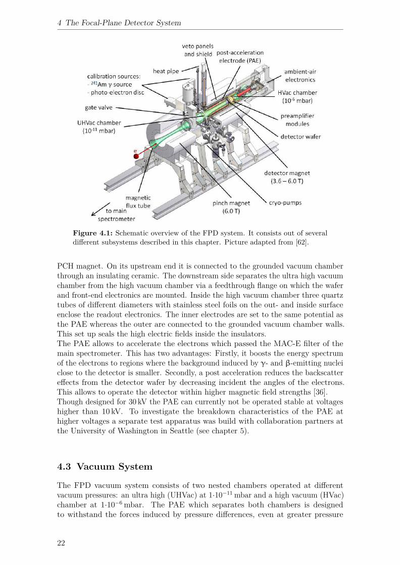
The Focal-Plane Detector system (FPD) located on the downstream side of the mainspectrometer guides electrons onto the detector wafer and consists of several sub-systems, listed in figure 4.1. The signal electrons follow the magnetic field provided bythe magnet system described in section 4.1. Before impinging on the detector waferthe electrons can be accelerated as described in section 4.2. To minimize scatteringof electrons with residual gas a suitable vacuum is needed which is provided bythe vacuum system (see section 4.3). The FPD system houses a cooling system(see section 4.4) in order to cool the detector wafer (section 4.5), and its read-outelectronics (section 4.6). A series of calibration sources allows to commission andcharacterize the detector prior to the data taking (see 4.7). To reduce the intrinsicbackground the wafer is surrounded by passive copper and lead shielding as well as arecently developed veto system described in section 4.8.
4.1 Magnet SystemThe FPD magnet system consists of two superconducting solenoids, the pinch (PCH)and detector (DET) magnet, which guide the signal electrons that passed the mainspectrometer (MS) onto the detector wafer. The PCH magnet, located directly onthe downstream end of the MS provides the maximum magnetic field strength in thewhole KATRIN beamline of Bmax = 6T. It is part of the MAC-E filter and is directlyrelated to the energy resolution of the spectrometer according to equation (3.3). Thedetector magnet (DET), located further downstream, can too provides fields up to6T but is usually operated with BDET<BPCH. It surrounds the detector wafer. Withthose nominal fields the magnetic flux at the wafer is 210Tcm2. By operating thePCH magnet at a higher field than the DET magnet electrons that do backscatterfrom the detector wafer are prevented from re-entering the main-spectrometer wherethey would induce additional background. To reach the superconducting state bothmagnets are cooled down with liquid helium and are held at 4.2K. This allows toswitch the magnets in a persistent mode after initial ramp-up. To compensate theattractive force between the magnets of 54 kN [55] spreader bars are installed inbetween.
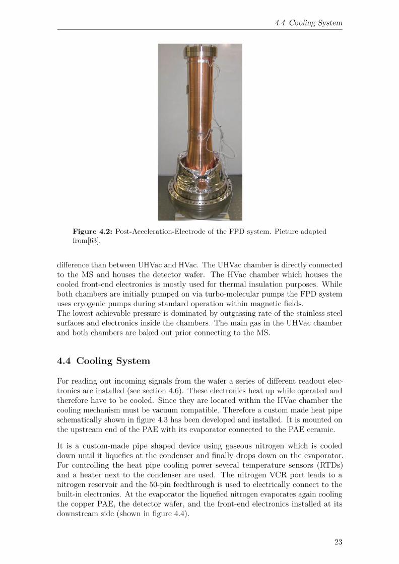
4.2 Post-Acceleration-ElectrodeThe Post-Acceleration-Electrode (PAE) is a full copper trumpet-shaped electrodewith a thickness of 3mm (shown in figure 4.2) located on the downstream side of the
21
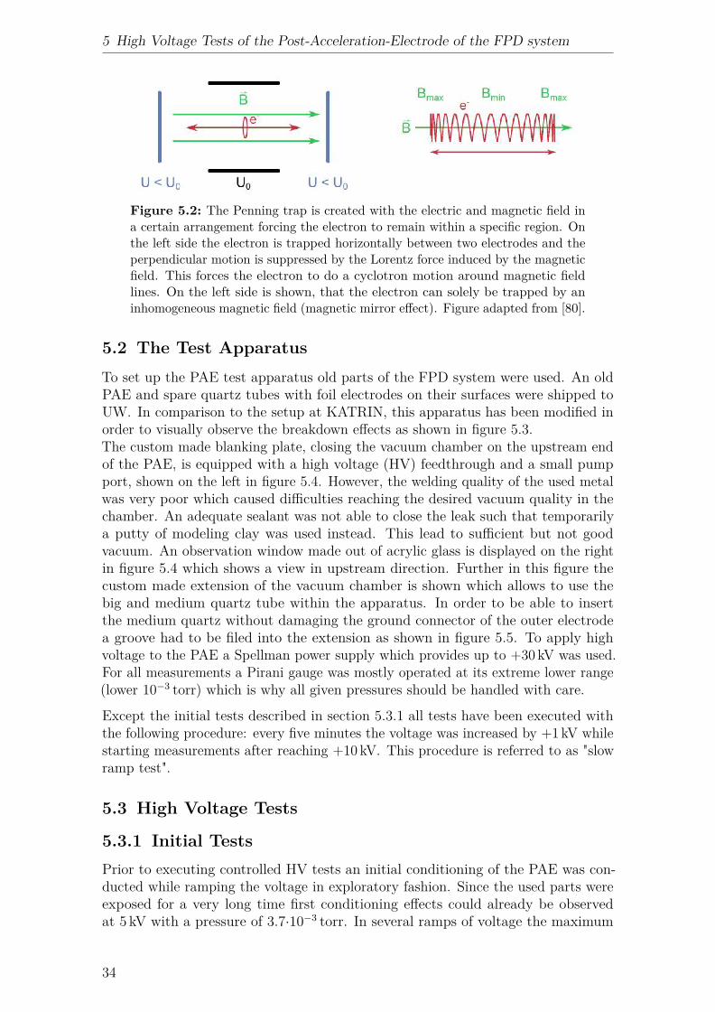
4 The Focal-Plane Detector System
Figure 4.1: Schematic overview of the FPD system. It consists out of severaldifferent subsystems described in this chapter. Picture adapted from [62].
PCH magnet. On its upstream end it is connected to the grounded vacuum chamberthrough an insulating ceramic. The downstream side separates the ultra high vacuumchamber from the high vacuum chamber via a feedthrough flange on which the waferand front-end electronics are mounted. Inside the high vacuum chamber three quartztubes of different diameters with stainless steel foils on the out- and inside surfaceenclose the readout electronics. The inner electrodes are set to the same potential asthe PAE whereas the outer are connected to the grounded vacuum chamber walls.This set up seals the high electric fields inside the insulators.The PAE allows to accelerate the electrons which passed the MAC-E filter of themain spectrometer. This has two advantages: Firstly, it boosts the energy spectrumof the electrons to regions where the background induced by γ- and β-emitting nucleiclose to the detector is smaller. Secondly, a post acceleration reduces the backscattereffects from the detector wafer by decreasing incident the angles of the electrons.This allows to operate the detector within higher magnetic field strengths [36].Though designed for 30 kV the PAE can currently not be operated stable at voltageshigher than 10 kV. To investigate the breakdown characteristics of the PAE athigher voltages a separate test apparatus was build with collaboration partners atthe University of Washington in Seattle (see chapter 5).
4.3 Vacuum System
The FPD vacuum system consists of two nested chambers operated at differentvacuum pressures: an ultra high (UHVac) at 1·10−11 mbar and a high vacuum (HVac)chamber at 1·10−6 mbar. The PAE which separates both chambers is designedto withstand the forces induced by pressure differences, even at greater pressure
22
4.4 Cooling System
Figure 4.2: Post-Acceleration-Electrode of the FPD system. Picture adaptedfrom[63].
difference than between UHVac and HVac. The UHVac chamber is directly connectedto the MS and houses the detector wafer. The HVac chamber which houses thecooled front-end electronics is mostly used for thermal insulation purposes. Whileboth chambers are initially pumped on via turbo-molecular pumps the FPD systemuses cryogenic pumps during standard operation within magnetic fields.The lowest achievable pressure is dominated by outgassing rate of the stainless steelsurfaces and electronics inside the chambers. The main gas in the UHVac chamberand both chambers are baked out prior connecting to the MS.
4.4 Cooling System
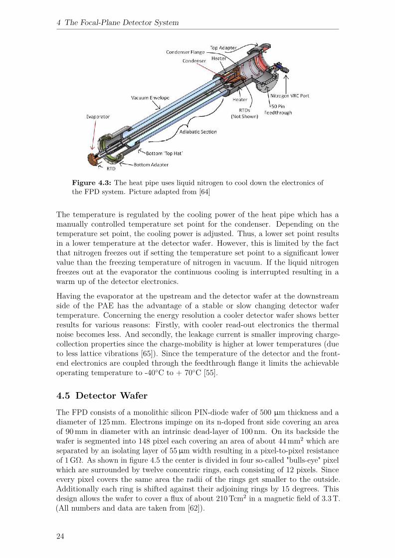
For reading out incoming signals from the wafer a series of different readout elec-tronics are installed (see section 4.6). These electronics heat up while operated andtherefore have to be cooled. Since they are located within the HVac chamber thecooling mechanism must be vacuum compatible. Therefore a custom made heat pipeschematically shown in figure 4.3 has been developed and installed. It is mounted onthe upstream end of the PAE with its evaporator connected to the PAE ceramic.
It is a custom-made pipe shaped device using gaseous nitrogen which is cooleddown until it liquefies at the condenser and finally drops down on the evaporator.For controlling the heat pipe cooling power several temperature sensors (RTDs)and a heater next to the condenser are used. The nitrogen VCR port leads to anitrogen reservoir and the 50-pin feedthrough is used to electrically connect to thebuilt-in electronics. At the evaporator the liquefied nitrogen evaporates again coolingthe copper PAE, the detector wafer, and the front-end electronics installed at itsdownstream side (shown in figure 4.4).
23
4 The Focal-Plane Detector System
Figure 4.3: The heat pipe uses liquid nitrogen to cool down the electronics ofthe FPD system. Picture adapted from [64]
The temperature is regulated by the cooling power of the heat pipe which has amanually controlled temperature set point for the condenser. Depending on thetemperature set point, the cooling power is adjusted. Thus, a lower set point resultsin a lower temperature at the detector wafer. However, this is limited by the factthat nitrogen freezes out if setting the temperature set point to a significant lowervalue than the freezing temperature of nitrogen in vacuum. If the liquid nitrogenfreezes out at the evaporator the continuous cooling is interrupted resulting in awarm up of the detector electronics.
Having the evaporator at the upstream and the detector wafer at the downstreamside of the PAE has the advantage of a stable or slow changing detector wafertemperature. Concerning the energy resolution a cooler detector wafer shows betterresults for various reasons: Firstly, with cooler read-out electronics the thermalnoise becomes less. And secondly, the leakage current is smaller improving charge-collection properties since the charge-mobility is higher at lower temperatures (dueto less lattice vibrations [65]). Since the temperature of the detector and the front-end electronics are coupled through the feedthrough flange it limits the achievableoperating temperature to -40C to + 70C [55].
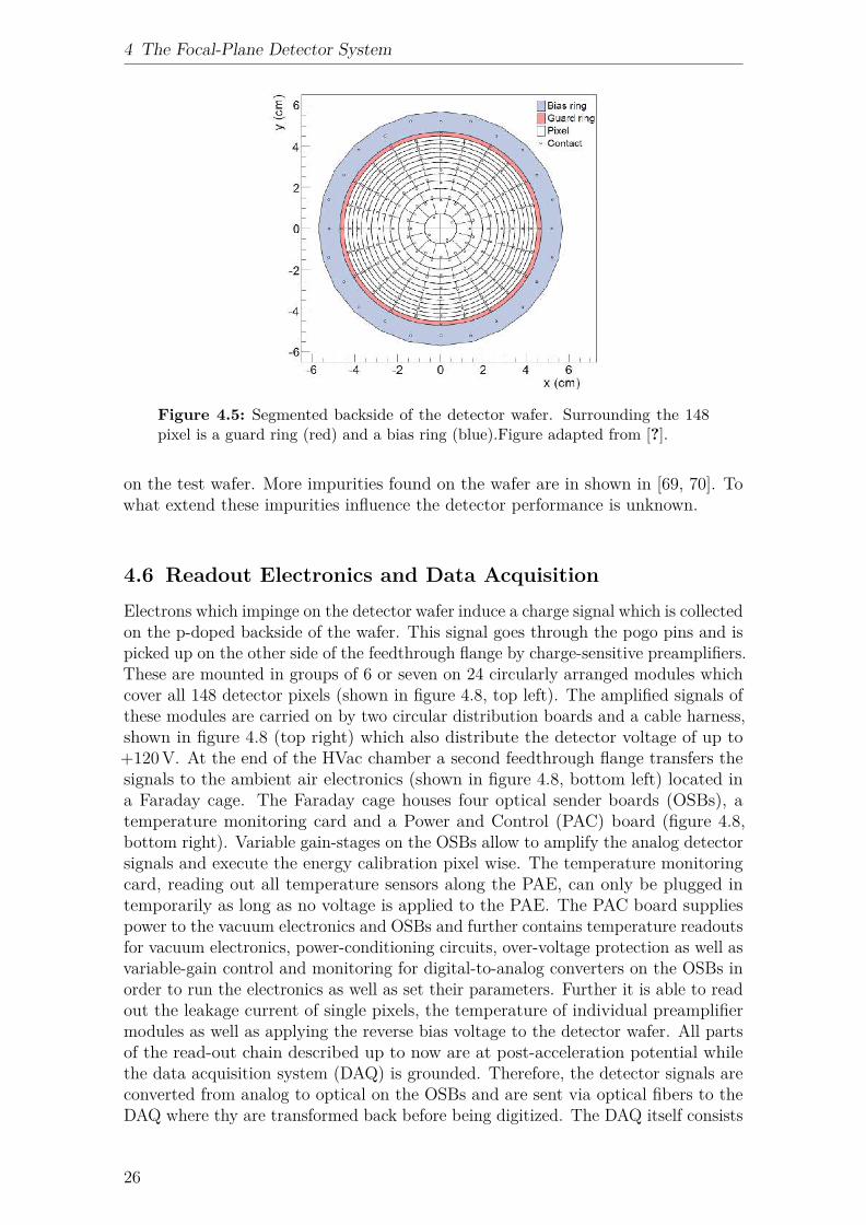
4.5 Detector WaferThe FPD consists of a monolithic silicon PIN-diode wafer of 500 µm thickness and adiameter of 125mm. Electrons impinge on its n-doped front side covering an areaof 90mm in diameter with an intrinsic dead-layer of 100 nm. On its backside thewafer is segmented into 148 pixel each covering an area of about 44mm2 which areseparated by an isolating layer of 55µm width resulting in a pixel-to-pixel resistanceof 1GΩ. As shown in figure 4.5 the center is divided in four so-called "bulls-eye" pixelwhich are surrounded by twelve concentric rings, each consisting of 12 pixels. Sinceevery pixel covers the same area the radii of the rings get smaller to the outside.Additionally each ring is shifted against their adjoining rings by 15 degrees. Thisdesign allows the wafer to cover a flux of about 210Tcm2 in a magnetic field of 3.3T.(All numbers and data are taken from [62]).
24
4.5 Detector Wafer
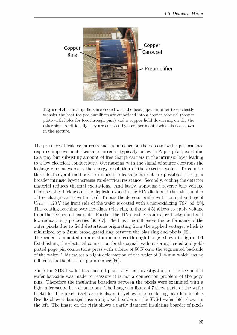
Figure 4.4: Pre-amplifiers are cooled with the heat pipe. In order to efficientlytransfer the heat the pre-amplifiers are embedded into a copper carousel (copperplate with holes for feedthrough pins) and a copper hold-down ring on the theother side. Additionally they are enclosed by a copper mantle which is not shownin the picture.
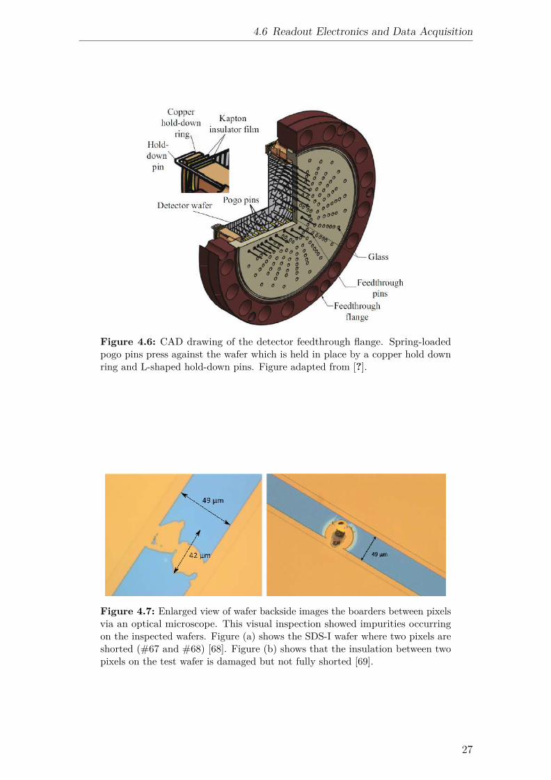
The presence of leakage currents and its influence on the detector wafer performancerequires improvement. Leakage currents, typically below 1nA per pixel, exist dueto a tiny but subsisting amount of free charge carriers in the intrinsic layer leadingto a low electrical conductivity. Overlapping with the signal of source electrons theleakage current worsens the energy resolution of the detector wafer. To counterthis effect several methods to reduce the leakage current are possible: Firstly, abroader intrinsic layer increases its electrical resistance. Secondly, cooling the detectormaterial reduces thermal excitations. And lastly, applying a reverse bias voltageincreases the thickness of the depletion zone in the PIN-diode and thus the numberof free charge carries within [55]. To bias the detector wafer with nominal voltage ofUbias = 120V the front side of the wafer is coated with a non-oxidizing TiN [66, 50].This coating reaching over the edges (bias ring in figure 4.5) allows to apply voltagefrom the segmented backside. Further the TiN coating assures low-background andlow-radioactivity properties [66, 67]. The bias ring influences the performance of theouter pixels due to field distortions originating from the applied voltage, which isminimized by a 2mm broad guard ring between the bias ring and pixels [62].The wafer is mounted on a custom made feedthrough flange, shown in figure 4.6.Establishing the electrical connection for the signal readout spring loaded and gold-plated pogo pin connections press with a force of 50N onto the segmented backsideof the wafer. This causes a slight deformation of the wafer of 0.24mm which has noinfluence on the detector performance [66].
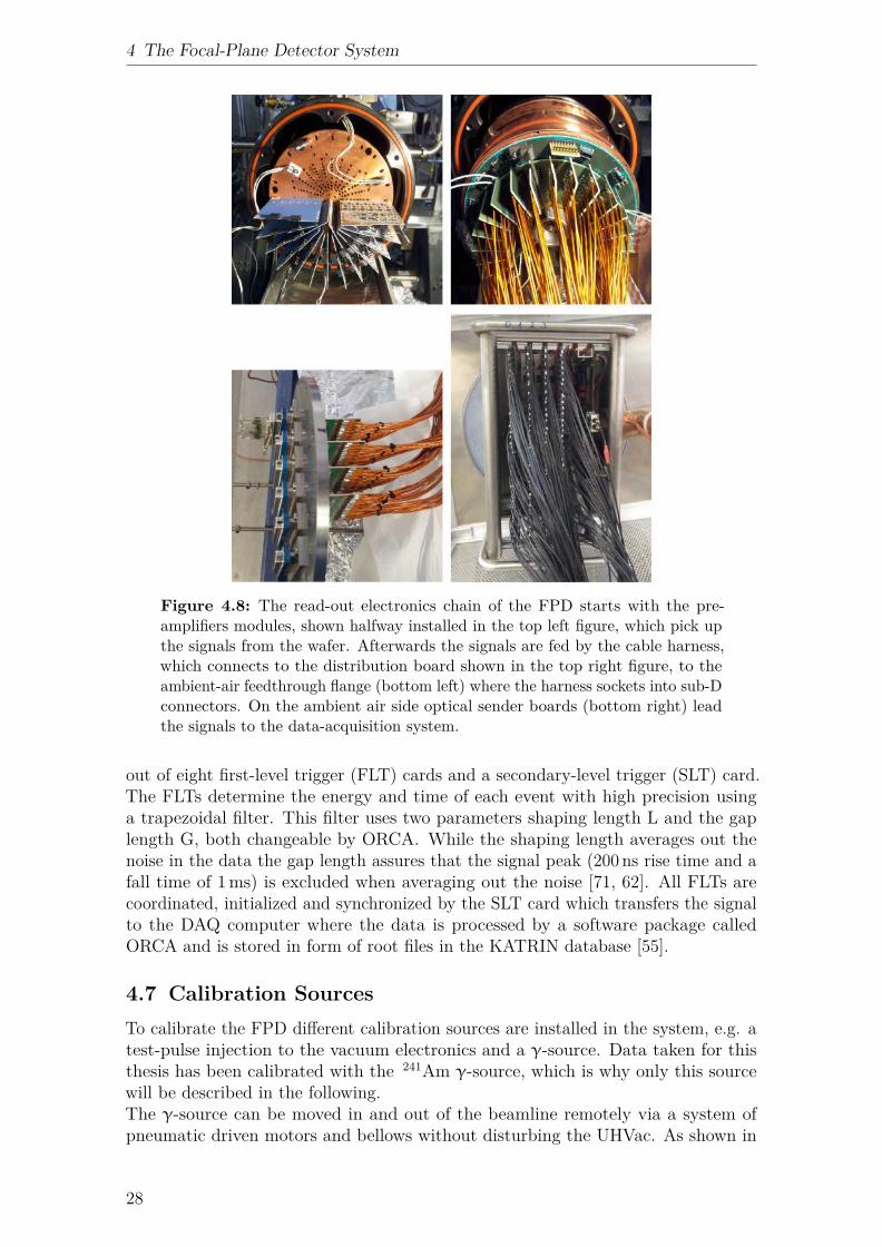
Since the SDS-I wafer has shorted pixels a visual investigation of the segmentedwafer backside was made to reassure it is not a connection problem of the pogopins. Therefore the insulating boarders between the pixels were examined with alight microscope in a clean room. The images in figure 4.7 show parts of the waferbackside: The pixels itself are displayed in yellow, the insulating boarders in blue.Results show a damaged insulating pixel boarder on the SDS-I wafer [68], shown inthe left. The image on the right shows a partly damaged insulating boarder of pixels
25
4 The Focal-Plane Detector System
Figure 4.5: Segmented backside of the detector wafer. Surrounding the 148pixel is a guard ring (red) and a bias ring (blue).Figure adapted from [?].
on the test wafer. More impurities found on the wafer are in shown in [69, 70]. Towhat extend these impurities influence the detector performance is unknown.
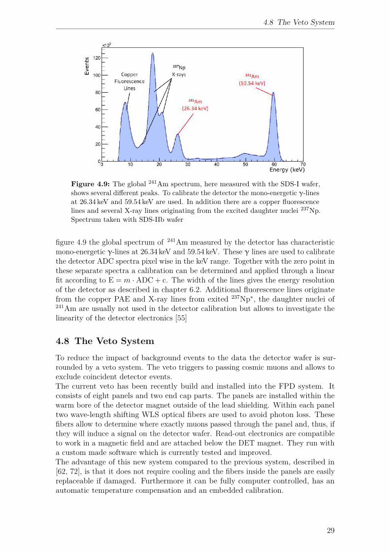
4.6 Readout Electronics and Data AcquisitionElectrons which impinge on the detector wafer induce a charge signal which is collectedon the p-doped backside of the wafer. This signal goes through the pogo pins and ispicked up on the other side of the feedthrough flange by charge-sensitive preamplifiers.These are mounted in groups of 6 or seven on 24 circularly arranged modules whichcover all 148 detector pixels (shown in figure 4.8, top left). The amplified signals ofthese modules are carried on by two circular distribution boards and a cable harness,shown in figure 4.8 (top right) which also distribute the detector voltage of up to+120V. At the end of the HVac chamber a second feedthrough flange transfers thesignals to the ambient air electronics (shown in figure 4.8, bottom left) located ina Faraday cage. The Faraday cage houses four optical sender boards (OSBs), atemperature monitoring card and a Power and Control (PAC) board (figure 4.8,bottom right). Variable gain-stages on the OSBs allow to amplify the analog detectorsignals and execute the energy calibration pixel wise. The temperature monitoringcard, reading out all temperature sensors along the PAE, can only be plugged intemporarily as long as no voltage is applied to the PAE. The PAC board suppliespower to the vacuum electronics and OSBs and further contains temperature readoutsfor vacuum electronics, power-conditioning circuits, over-voltage protection as well asvariable-gain control and monitoring for digital-to-analog converters on the OSBs inorder to run the electronics as well as set their parameters. Further it is able to readout the leakage current of single pixels, the temperature of individual preamplifiermodules as well as applying the reverse bias voltage to the detector wafer. All partsof the read-out chain described up to now are at post-acceleration potential whilethe data acquisition system (DAQ) is grounded. Therefore, the detector signals areconverted from analog to optical on the OSBs and are sent via optical fibers to theDAQ where thy are transformed back before being digitized. The DAQ itself consists
26
4.6 Readout Electronics and Data Acquisition
Figure 4.6: CAD drawing of the detector feedthrough flange. Spring-loadedpogo pins press against the wafer which is held in place by a copper hold downring and L-shaped hold-down pins. Figure adapted from [?].
Figure 4.7: Enlarged view of wafer backside images the boarders between pixelsvia an optical microscope. This visual inspection showed impurities occurringon the inspected wafers. Figure (a) shows the SDS-I wafer where two pixels areshorted (#67 and #68) [68]. Figure (b) shows that the insulation between twopixels on the test wafer is damaged but not fully shorted [69].
27
4 The Focal-Plane Detector System
Figure 4.8: The read-out electronics chain of the FPD starts with the pre-amplifiers modules, shown halfway installed in the top left figure, which pick upthe signals from the wafer. Afterwards the signals are fed by the cable harness,which connects to the distribution board shown in the top right figure, to theambient-air feedthrough flange (bottom left) where the harness sockets into sub-Dconnectors. On the ambient air side optical sender boards (bottom right) leadthe signals to the data-acquisition system.
out of eight first-level trigger (FLT) cards and a secondary-level trigger (SLT) card.The FLTs determine the energy and time of each event with high precision usinga trapezoidal filter. This filter uses two parameters shaping length L and the gaplength G, both changeable by ORCA. While the shaping length averages out thenoise in the data the gap length assures that the signal peak (200 ns rise time and afall time of 1ms) is excluded when averaging out the noise [71, 62]. All FLTs arecoordinated, initialized and synchronized by the SLT card which transfers the signalto the DAQ computer where the data is processed by a software package calledORCA and is stored in form of root files in the KATRIN database [55].
4.7 Calibration SourcesTo calibrate the FPD different calibration sources are installed in the system, e.g. atest-pulse injection to the vacuum electronics and a γ-source. Data taken for thisthesis has been calibrated with the 241Am γ-source, which is why only this sourcewill be described in the following.The γ-source can be moved in and out of the beamline remotely via a system ofpneumatic driven motors and bellows without disturbing the UHVac. As shown in
28
4.8 The Veto System
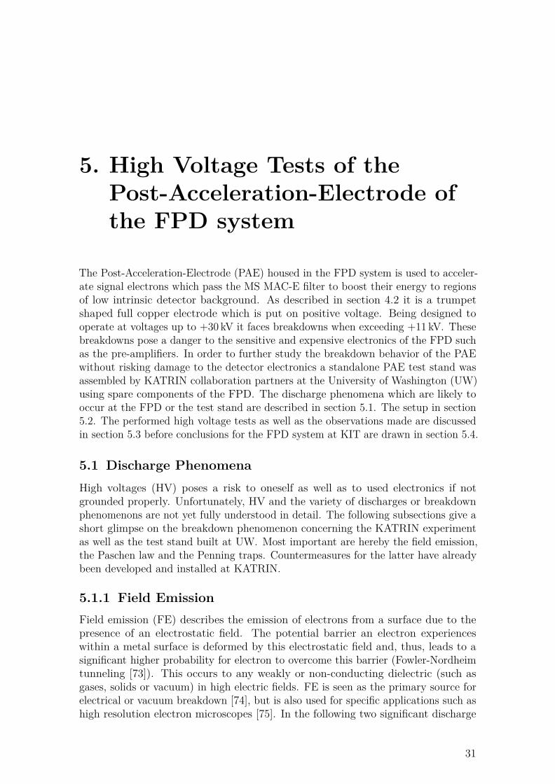
Figure 4.9: The global 241Am spectrum, here measured with the SDS-I wafer,shows several different peaks. To calibrate the detector the mono-energetic γ-linesat 26.34 keV and 59.54 keV are used. In addition there are a copper fluorescencelines and several X-ray lines originating from the excited daughter nuclei 237Np.Spectrum taken with SDS-IIb wafer
figure 4.9 the global spectrum of 241Am measured by the detector has characteristicmono-energetic γ-lines at 26.34 keV and 59.54 keV. These γ lines are used to calibratethe detector ADC spectra pixel wise in the keV range. Together with the zero point inthese separate spectra a calibration can be determined and applied through a linearfit according to E = m ·ADC + c. The width of the lines gives the energy resolutionof the detector as described in chapter 6.2. Additional fluorescence lines originatefrom the copper PAE and X-ray lines from exited 237Np∗, the daughter nuclei of241Am are usually not used in the detector calibration but allows to investigate thelinearity of the detector electronics [55]
4.8 The Veto System
To reduce the impact of background events to the data the detector wafer is sur-rounded by a veto system. The veto triggers to passing cosmic muons and allows toexclude coincident detector events.The current veto has been recently build and installed into the FPD system. Itconsists of eight panels and two end cap parts. The panels are installed within thewarm bore of the detector magnet outside of the lead shielding. Within each paneltwo wave-length shifting WLS optical fibers are used to avoid photon loss. Thesefibers allow to determine where exactly muons passed through the panel and, thus, ifthey will induce a signal on the detector wafer. Read-out electronics are compatibleto work in a magnetic field and are attached below the DET magnet. They run witha custom made software which is currently tested and improved.The advantage of this new system compared to the previous system, described in[62, 72], is that it does not require cooling and the fibers inside the panels are easilyreplaceable if damaged. Furthermore it can be fully computer controlled, has anautomatic temperature compensation and an embedded calibration.
29

5. High Voltage Tests of thePost-Acceleration-Electrode ofthe FPD system
The Post-Acceleration-Electrode (PAE) housed in the FPD system is used to acceler-ate signal electrons which pass the MS MAC-E filter to boost their energy to regionsof low intrinsic detector background. As described in section 4.2 it is a trumpetshaped full copper electrode which is put on positive voltage. Being designed tooperate at voltages up to +30 kV it faces breakdowns when exceeding +11 kV. Thesebreakdowns pose a danger to the sensitive and expensive electronics of the FPD suchas the pre-amplifiers. In order to further study the breakdown behavior of the PAEwithout risking damage to the detector electronics a standalone PAE test stand wasassembled by KATRIN collaboration partners at the University of Washington (UW)using spare components of the FPD. The discharge phenomena which are likely tooccur at the FPD or the test stand are described in section 5.1. The setup in section5.2. The performed high voltage tests as well as the observations made are discussedin section 5.3 before conclusions for the FPD system at KIT are drawn in section 5.4.
5.1 Discharge PhenomenaHigh voltages (HV) poses a risk to oneself as well as to used electronics if notgrounded properly. Unfortunately, HV and the variety of discharges or breakdownphenomenons are not yet fully understood in detail. The following subsections give ashort glimpse on the breakdown phenomenon concerning the KATRIN experimentas well as the test stand built at UW. Most important are hereby the field emission,the Paschen law and the Penning traps. Countermeasures for the latter have alreadybeen developed and installed at KATRIN.
5.1.1 Field EmissionField emission (FE) describes the emission of electrons from a surface due to thepresence of an electrostatic field. The potential barrier an electron experienceswithin a metal surface is deformed by this electrostatic field and, thus, leads to asignificant higher probability for electron to overcome this barrier (Fowler-Nordheimtunneling [73]). This occurs to any weakly or non-conducting dielectric (such asgases, solids or vacuum) in high electric fields. FE is seen as the primary source forelectrical or vacuum breakdown [74], but is also used for specific applications such ashigh resolution electron microscopes [75]. In the following two significant discharge
31
5 High Voltage Tests of the Post-Acceleration-Electrode of the FPD system
mechanisms are described.
Townsend MechanismIn high vacuum the discharge is described by the Townsend mechanism: An electron,which has overcome the potential barrier, is accelerated by the applied electric field.If the mean free path of the electron is long enough it is able to gain enough energybefore colliding with residual atoms which it then ionizes creating secondary electrons(SE) and ions. The required voltage for this process depends on the residual gas.These SE are also accelerated by the potential of the electric field and cause furtherionization (avalanche effect). Discharges based on the Townsend mechanism are selfsustaining if the power supply keeps providing current [76].
Vacuum breakdownA vacuum breakdown is initiated by field emission from microprotrusions on anelectrode surface within a good vacuum and no magnetic field. Microprotrusionsare small tips at which the electric field is enhanced. A higher field can induce localheating which leads to melting of the surface in this particular spot building metalvapor which then locally degrades the vacuum and can result in gaseous breakdownwith ionization. This shows how important it is for a system to have smooth surfaceswhen operating with HV in order to avoid breakdowns. Smoothening the surface canbe achieved by electro- or mechanical polishing as well as via ion bombardment. Vac-uum breakdowns are a surface dominated phenomenon depending on the propertiesof the used material, thus, residual gases as well as the presence of a magnetic fieldhave an minor influence [76]. The breakdown is a voltage dependent phenomenondescribed by the Paschen Law for a certain vacuum pressure regime (see section 5.1.2).
Triple JunctionsTriple junctions are an intersection of a metallic surface with a dielectric surfacelocated within a vacuum. It can cause field enhancements initiating a discharge (viasurface avalanche effects) already in relatively low electric fields. In high voltagesystems the insulators surfaces are the weakest components because they are agood source of ionizable material and discharges preferably propagate along surfaces.Further field enhancements fostering discharges may be caused via charged insulatorsurfaces from previous discharges, since the charge is not able to redistribute itselfdue to its non-conducting properties. Triple junctions are not yet fully understoodnor described but show a notable influence when operating with HV.
5.1.2 Paschen LawThe Paschen law describes the breakdown voltage between electrodes as a functionof vacuum pressure and gap length. The equation was empirically discovered in 1889[77]:
V = B · p · dln (A · p · d)− ln (ln (1 + γ−1
se )) (5.1)
Deriving this equation shows the associated Paschen curve has a minimum, illustratedin figure 5.1. For small p·d (left side of the minimum) the electrons gain enoughenergy to ionize atoms, however, their mean free path is very large and so it becomes
32
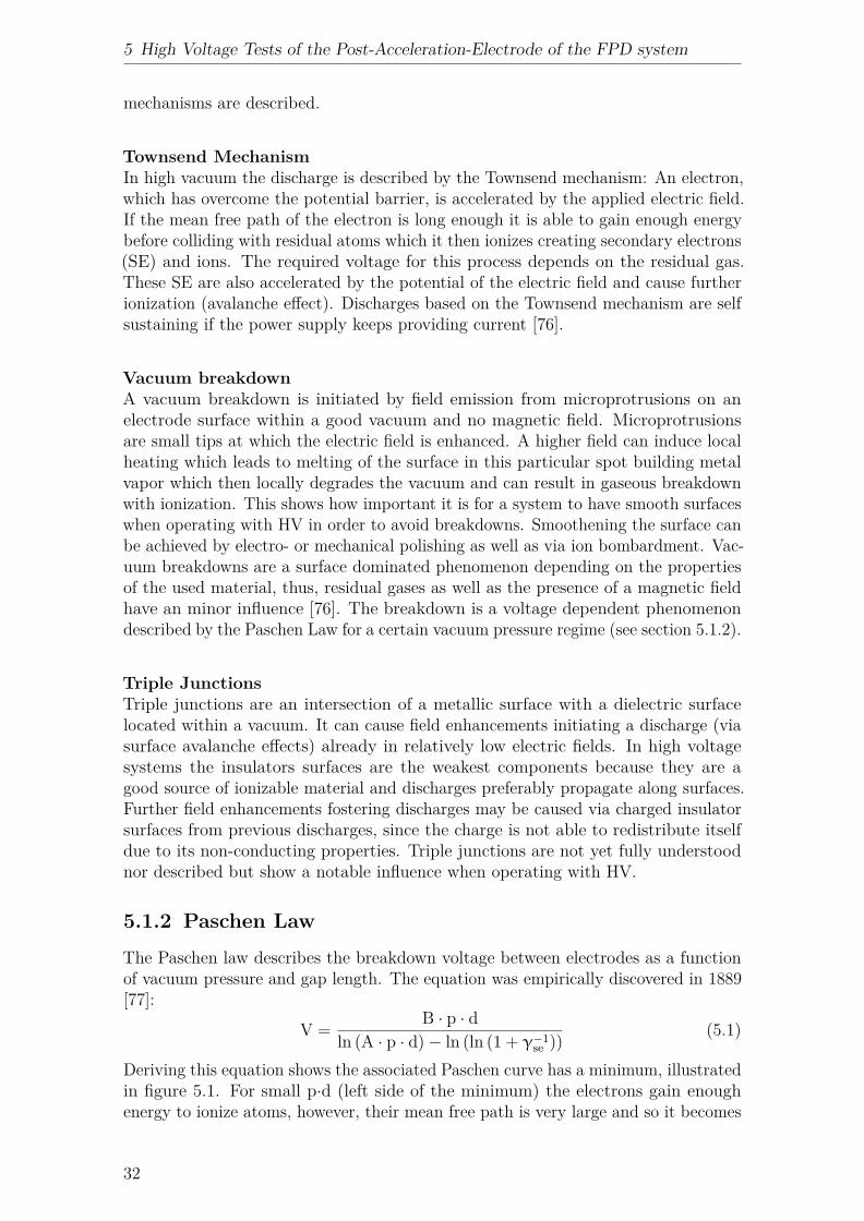
5.1 Discharge Phenomena
p d.
V
10 10 mbar-6 -3-
Figure 5.1: The Paschen curve illustrated, shows schematically the breakdownvoltage as a function of pressure and electrode distance p·d. The exact positionof the minimum depends the residual gas and the material of used electrodesin the vacuum system. For low pressures the number of gas atoms is low and,thus, the probability of a collision is low resulting in less ionization. At higherpressures the mean free path of the electron is too short to obtain enough energyfor ionizing other atoms. Figure adapted from [78].
more likely for these electrons to reach an electrode rather than ionize an atom. Thisresults in an increase of the breakdown voltage. On the other side of the minimum,a higher gas pressure results in a shorter mean free path for the electrons. Witha higher probability of collisions the electrons are unable to gain enough energy inorder to ionize atoms. Further, with each collision the electron trajectory is forced tochange the direction. Therefore, the breakdown voltage increases for higher p·d.However, the exact course of the function as well as the position of the minimumdepends on the gas type as well as the electrode material.
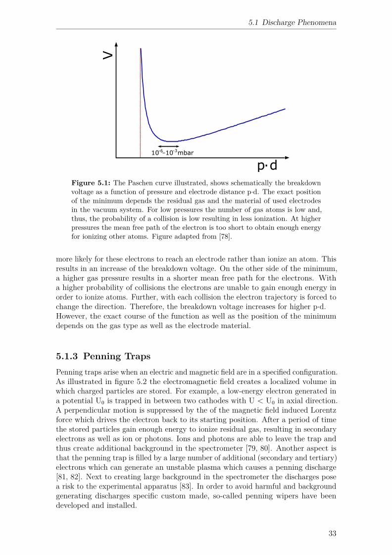
5.1.3 Penning TrapsPenning traps arise when an electric and magnetic field are in a specified configuration.As illustrated in figure 5.2 the electromagnetic field creates a localized volume inwhich charged particles are stored. For example, a low-energy electron generated ina potential U0 is trapped in between two cathodes with U < U0 in axial direction.A perpendicular motion is suppressed by the of the magnetic field induced Lorentzforce which drives the electron back to its starting position. After a period of timethe stored particles gain enough energy to ionize residual gas, resulting in secondaryelectrons as well as ion or photons. Ions and photons are able to leave the trap andthus create additional background in the spectrometer [79, 80]. Another aspect isthat the penning trap is filled by a large number of additional (secondary and tertiary)electrons which can generate an unstable plasma which causes a penning discharge[81, 82]. Next to creating large background in the spectrometer the discharges posea risk to the experimental apparatus [83]. In order to avoid harmful and backgroundgenerating discharges specific custom made, so-called penning wipers have beendeveloped and installed.
33
5 High Voltage Tests of the Post-Acceleration-Electrode of the FPD system
Figure 5.2: The Penning trap is created with the electric and magnetic field ina certain arrangement forcing the electron to remain within a specific region. Onthe left side the electron is trapped horizontally between two electrodes and theperpendicular motion is suppressed by the Lorentz force induced by the magneticfield. This forces the electron to do a cyclotron motion around magnetic fieldlines. On the left side is shown, that the electron can solely be trapped by aninhomogeneous magnetic field (magnetic mirror effect). Figure adapted from [80].
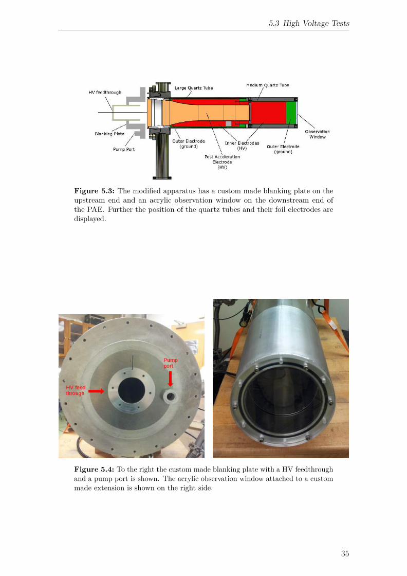
5.2 The Test ApparatusTo set up the PAE test apparatus old parts of the FPD system were used. An oldPAE and spare quartz tubes with foil electrodes on their surfaces were shipped toUW. In comparison to the setup at KATRIN, this apparatus has been modified inorder to visually observe the breakdown effects as shown in figure 5.3.The custom made blanking plate, closing the vacuum chamber on the upstream endof the PAE, is equipped with a high voltage (HV) feedthrough and a small pumpport, shown on the left in figure 5.4. However, the welding quality of the used metalwas very poor which caused difficulties reaching the desired vacuum quality in thechamber. An adequate sealant was not able to close the leak such that temporarilya putty of modeling clay was used instead. This lead to sufficient but not goodvacuum. An observation window made out of acrylic glass is displayed on the rightin figure 5.4 which shows a view in upstream direction. Further in this figure thecustom made extension of the vacuum chamber is shown which allows to use thebig and medium quartz tube within the apparatus. In order to be able to insertthe medium quartz without damaging the ground connector of the outer electrodea groove had to be filed into the extension as shown in figure 5.5. To apply highvoltage to the PAE a Spellman power supply which provides up to +30 kV was used.For all measurements a Pirani gauge was mostly operated at its extreme lower range(lower 10−3 torr) which is why all given pressures should be handled with care.
Except the initial tests described in section 5.3.1 all tests have been executed withthe following procedure: every five minutes the voltage was increased by +1 kV whilestarting measurements after reaching +10 kV. This procedure is referred to as "slowramp test".
5.3 High Voltage Tests
5.3.1 Initial TestsPrior to executing controlled HV tests an initial conditioning of the PAE was con-ducted while ramping the voltage in exploratory fashion. Since the used parts wereexposed for a very long time first conditioning effects could already be observedat 5 kV with a pressure of 3.7·10−3 torr. In several ramps of voltage the maximum
34
5.3 High Voltage Tests
Figure 5.3: The modified apparatus has a custom made blanking plate on theupstream end and an acrylic observation window on the downstream end ofthe PAE. Further the position of the quartz tubes and their foil electrodes aredisplayed.
Figure 5.4: To the right the custom made blanking plate with a HV feedthroughand a pump port is shown. The acrylic observation window attached to a custommade extension is shown on the right side.
35
5 High Voltage Tests of the Post-Acceleration-Electrode of the FPD system
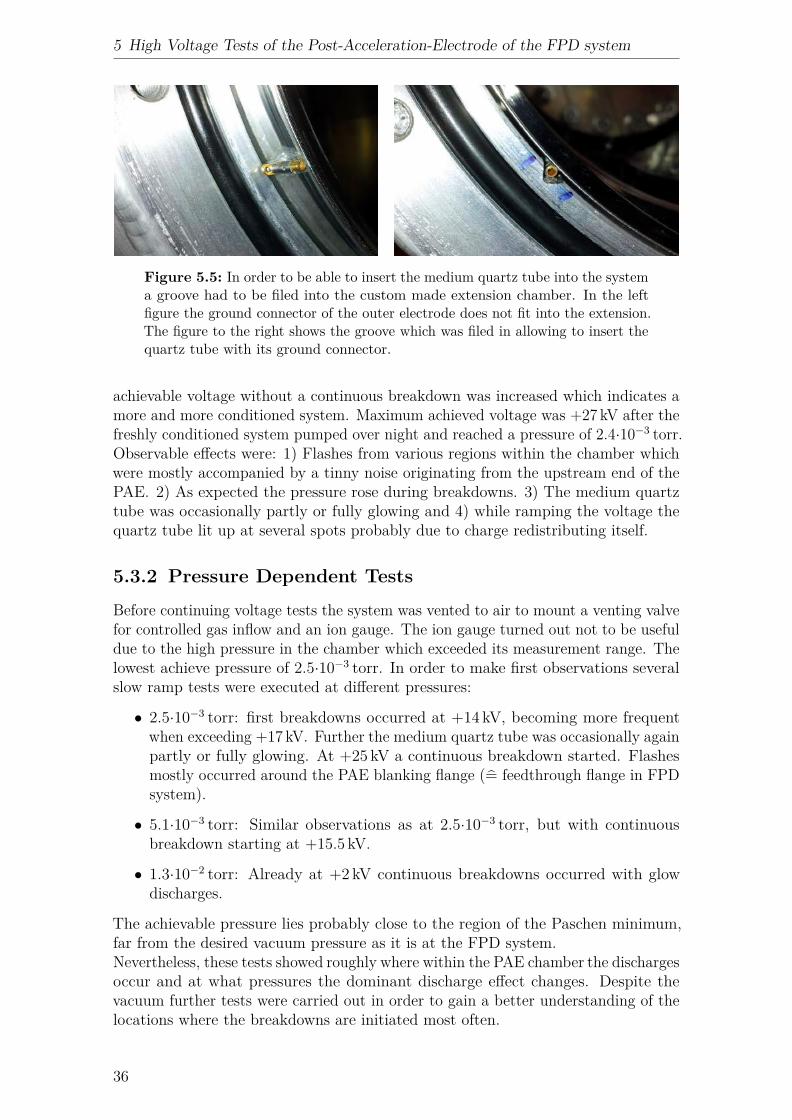
Figure 5.5: In order to be able to insert the medium quartz tube into the systema groove had to be filed into the custom made extension chamber. In the leftfigure the ground connector of the outer electrode does not fit into the extension.The figure to the right shows the groove which was filed in allowing to insert thequartz tube with its ground connector.
achievable voltage without a continuous breakdown was increased which indicates amore and more conditioned system. Maximum achieved voltage was +27 kV after thefreshly conditioned system pumped over night and reached a pressure of 2.4·10−3 torr.Observable effects were: 1) Flashes from various regions within the chamber whichwere mostly accompanied by a tinny noise originating from the upstream end of thePAE. 2) As expected the pressure rose during breakdowns. 3) The medium quartztube was occasionally partly or fully glowing and 4) while ramping the voltage thequartz tube lit up at several spots probably due to charge redistributing itself.
5.3.2 Pressure Dependent Tests
Before continuing voltage tests the system was vented to air to mount a venting valvefor controlled gas inflow and an ion gauge. The ion gauge turned out not to be usefuldue to the high pressure in the chamber which exceeded its measurement range. Thelowest achieve pressure of 2.5·10−3 torr. In order to make first observations severalslow ramp tests were executed at different pressures:
• 2.5·10−3 torr: first breakdowns occurred at +14 kV, becoming more frequentwhen exceeding +17 kV. Further the medium quartz tube was occasionally againpartly or fully glowing. At +25 kV a continuous breakdown started. Flashesmostly occurred around the PAE blanking flange (= feedthrough flange in FPDsystem).
• 5.1·10−3 torr: Similar observations as at 2.5·10−3 torr, but with continuousbreakdown starting at +15.5 kV.
• 1.3·10−2 torr: Already at +2 kV continuous breakdowns occurred with glowdischarges.
The achievable pressure lies probably close to the region of the Paschen minimum,far from the desired vacuum pressure as it is at the FPD system.Nevertheless, these tests showed roughly where within the PAE chamber the dischargesoccur and at what pressures the dominant discharge effect changes. Despite thevacuum further tests were carried out in order to gain a better understanding of thelocations where the breakdowns are initiated most often.
36
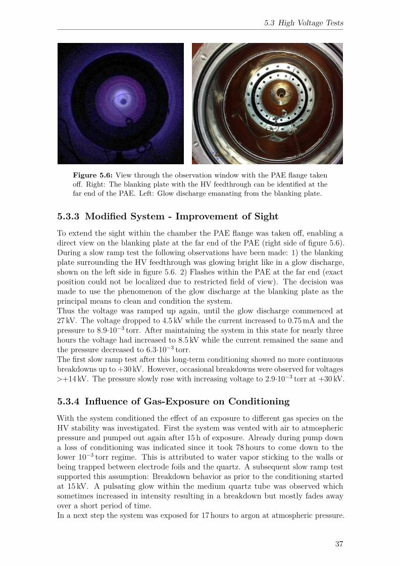
5.3 High Voltage Tests
Figure 5.6: View through the observation window with the PAE flange takenoff. Right: The blanking plate with the HV feedthrough can be identified at thefar end of the PAE. Left: Glow discharge emanating from the blanking plate.
5.3.3 Modified System - Improvement of SightTo extend the sight within the chamber the PAE flange was taken off, enabling adirect view on the blanking plate at the far end of the PAE (right side of figure 5.6).During a slow ramp test the following observations have been made: 1) the blankingplate surrounding the HV feedthrough was glowing bright like in a glow discharge,shown on the left side in figure 5.6. 2) Flashes within the PAE at the far end (exactposition could not be localized due to restricted field of view). The decision wasmade to use the phenomenon of the glow discharge at the blanking plate as theprincipal means to clean and condition the system.Thus the voltage was ramped up again, until the glow discharge commenced at27 kV. The voltage dropped to 4.5 kV while the current increased to 0.75mA and thepressure to 8.9·10−3 torr. After maintaining the system in this state for nearly threehours the voltage had increased to 8.5 kV while the current remained the same andthe pressure decreased to 6.3·10−3 torr.The first slow ramp test after this long-term conditioning showed no more continuousbreakdowns up to +30 kV. However, occasional breakdowns were observed for voltages>+14 kV. The pressure slowly rose with increasing voltage to 2.9·10−3 torr at +30 kV.
5.3.4 Influence of Gas-Exposure on ConditioningWith the system conditioned the effect of an exposure to different gas species on theHV stability was investigated. First the system was vented with air to atmosphericpressure and pumped out again after 15 h of exposure. Already during pump downa loss of conditioning was indicated since it took 78 hours to come down to thelower 10−3 torr regime. This is attributed to water vapor sticking to the walls orbeing trapped between electrode foils and the quartz. A subsequent slow ramp testsupported this assumption: Breakdown behavior as prior to the conditioning startedat 15 kV. A pulsating glow within the medium quartz tube was observed whichsometimes increased in intensity resulting in a breakdown but mostly fades awayover a short period of time.In a next step the system was exposed for 17 hours to argon at atmospheric pressure.
37
5 High Voltage Tests of the Post-Acceleration-Electrode of the FPD system
After pumping for 2 hours the pressure reached 2.6·10−3 torr again. A slow ramptest showed again the previously observed breakdown behavior: First breakdowns at+17 kV followed by a more frequent appearance when exceeding 22 kV. Even whenexposing the system for a short period time, e.g. during quick modifications at thevacuum system a loss of conditioning could be observed.
5.3.5 Observations - SummarizedSeveral different phenomena were observed during HV breakdowns of the PAE:
• When significant breakdowns occur the pressure may rise by up to an order ofmagnitude.
• At moderate voltages (<20 kV) flashes mainly occurred behind the PAE flange(determined through bolt holes of this flange). At higher voltages (>20 kV)flashes also appeared close to the observation window.
• Nearly all of the flashes are accompanied by a tinny noise originating from thefar end of the system (around PAE ceramic).
• The medium quartz tube occasionally began to glow party or fully. Thiscould be due to fluorescence of the quartz glass or when it functions as a lightconductor. This glow lasted between a few seconds and a couple of minutes. Inaddition a pulsating glow was observed which tended to fade away over time,but occasionally increased in intensity and resulted in a discharge.
• Massive discharges were accompanied by the HV cable lighting up over a lengthof up to 50 cm. This could cause damage to any electronics which are connectedto or touching the cable. Further these discharges produce RF noise whichcan be picked up by cables or other parts of electric devices functioning asantenna and in this way harm electronics or generate noise in the detectorsignals. E.g. during the tests the sensitive input FET of the ion gauge controllerwas destroyed twice, and the more robust Pirani gauge readout displayed a"fault" error frequently after discharges.
• Small lit up spots were observed during ramping the voltage up or down. Thiscould be due to charge accumulation on the insulator surface (quartz) before itredistributes itself.
• Glow discharges that emanate from the blanking plate could be observedand were utilized to condition the system. This process removes residualcontaminations such as water vapor, oxygen or residuals of the sealant adheringto the chamber walls. After conditioning no more continuous glow dischargeswere observed at pressures of ∼10−3 Torr and for voltages up to +30 kV.
• The observation window was bombarded by ions emitted by the glow dischargeat the blanking plate. Since the window acts as an insulator the chargeaccumulated which leads to surface discharges towards the metallic extensionchamber, there, causing a bright flash.
When dismantling the system the used sealant was found not to be cured. Thisprobably induced a vapor pressure explaining the rather poor vacuum quality of thesystem. In addition, sharp edges, which are known to enhance electric fields, were
38

5.4 Conclusion
Figure 5.7: The left figure shows that notches have been cut out of the outerelectrode foil on the medium quartz tube. The notches are located in a high fieldregion according to [84]. The right figure shows where the sealant penetratedinto the vacuum chamber can be seen.
Figure 5.8: The stainless steel support saddle is supporting the big quartz tube.Right: design of the saddle and supposed position within the vacuum chamber.Left: the inner electrode of the big quartz tube has a direct line-of-sight onto thegrounded saddle.
found within high field regions according to [84] on the outer electrode of the quartztubes, especially at the medium one. As shown in figure 5.7 part of the electrodehas been cut out. Another potential reason for the HV breakdowns could be thedirect line-of-sight. Surface discharges exist and tend to go to components which areat a different electric potential such as the grounded stainless steel support saddle.Figure 5.8 shows the latter in the intended position.
5.4 ConclusionFurther studies at lower pressures are required to fully understand the PAE break-downs above 10 kV. However the following conclusions can be drawn from the firstseries of test measurements at poor vacuum:
• A power supply which does not trip off during continuous breakdowns is requiredfor effective conditioning.
• The most effective conditioning is achieved by initiating a glow discharge at apressure of ∼10−2 Torr. This discharge should be continued until the pressureand current read-back begin to fall.
39
5 High Voltage Tests of the Post-Acceleration-Electrode of the FPD system
• HV breakdowns of the PAE can harm the sensitive electronics. No attemptshould be made to condition the PAE when the pre-amplifiers are installed.It is quite possible that equipment like pressure gauges, RGA’s, Pulcinellaelectronics, and equipment associated with the magnets etc. could be damaged.
• After long-term conditioning, even though voltages of +30 kV were achievedwithout continuous breakdown, intermittent breakdowns occurred every fewminutes. These would probably pose a risk the electronics as well.
• Despite the limited visibility it appears that most of the sparks come from theregion just behind the PAE flange, and to some extent from the far end ofthe PAE where the large quartz tube sockets into the insulator ring. Both areregions where high fields, as identified in [84], and triple junctions exist.
For upcoming measurements with the PAE test stand at UW a new, leak freeblanking plate should be build in order to operate the system under realistic vacuumconditions which are similar to the FPD system. Furthermore, the breakdownsshould be investigated as a function of foil-electrode position on the quartz tube.For reproducibility reasons and ease of operation the ramping of voltage shouldbe automated. An automated way of recording breakdowns as a function of time,in combination with a camera looking through the window would be a powerfulimprovement of the system in terms of data taking.
40
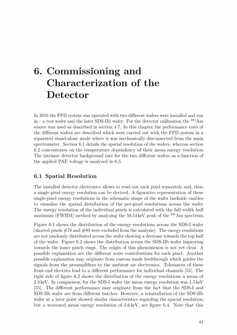
6. Commissioning andCharacterization of theDetector
In 2016 the FPD system was operated with two different wafers were installed and runin : a test wafer and the later SDS-IIb wafer. For the detector calibration the 241Amsource was used as described in section 4.7. In this chapter the performance tests ofthe different wafers are described which were carried out with the FPD system in aseparated stand-alone mode where it was mechanically disconnected from the mainspectrometer. Section 6.1 details the spatial resolution of the wafers, whereas section6.2 concentrates on the temperature dependency of their mean energy resolution.The intrinsic detector background rate for the two different wafers as a function ofthe applied PAE voltage is analyzed in 6.3.
6.1 Spatial Resolution
The installed detector electronics allows to read out each pixel separately and, thus,a single-pixel energy resolution can be derived. A figurative representation of thesesingle-pixel energy resolutions in the schematic shape of the wafer backside enablesto visualize the spatial distribution of the per-pixel resolutions across the wafer.The energy resolution of the individual pixels is calculated with the full width halfmaximum (FWHM) method by analyzing the 59.54 keV peak of the 241Am spectrum.
Figure 6.1 shows the distribution of the energy resolutions across the SDS-I wafer(shorted pixels #78 and #89 were excluded from the analysis). The energy resolutionsare not randomly distributed across the wafer showing a decrease towards the top halfof the wafer. Figure 6.2 shows the distribution across the SDS-IIb wafer improvingtowards the inner pixels rings. The origin of this phenomenon is not yet clear. Apossible explanation are the different noise contributions for each pixel. Anotherpossible explanation may originate from custom made feedthrough which guides thesignals from the preamplifiers to the ambient air electronics. Tolerances of thesefront-end electrics lead to a different performance for individual channels [55]. Theright side of figure 6.2 shows the distribution of the energy resolutions a mean of2.3 keV. In comparison, for the SDS-I wafer the mean energy resolution was 1.5 keV[55]. The different performance may originate from the fact that the SDS-I andSDS-IIb wafer are from different batches. However, a reinstallation of the SDS-IIbwafer at a later point showed similar characteristics regarding the spacial resolution,but a worsened mean energy resolution of 2.6 keV, see figure 6.4. Note that this
41
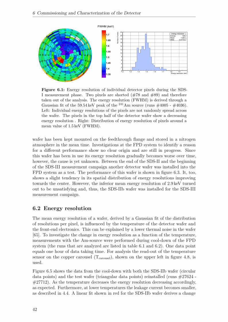
6 Commissioning and Characterization of the Detector
1.35
1.4
1.45
1.5
1.55
1.6
1.65
1.7
01
2 3
45
678
910
11
12 1314
15
16
17
1819
20
2122
23
24 25
26
27
28
29
3031
32
3334
35
3637
38
39
40
41
4243
44
4546
47
48 49
50
51
52
53
54
55
56
57
58
59
60
61
62
63
64
65
6667
68
6970
71
72 73
74
75
76
77
78
79
80
81
82
83
84
85
86
87
88
89
9091
92
9394
95
96 97
98
99
100
101
102
103
104
105
106
107
108
109
110
111
112
113
114115
116
117
118
119
120 121
122
123
124
125
126
127
128
129
130
131
132
133
134
135
136
137
138139
140
141
142
143
144 145
146
147
FWHM xkeV)
EnergyresolutionEntries 148Mean 1.483RMS 0.07753
Energy resolution xkeV)1.2 1.3 1.4 1.5 1.6 1.7 1.8 1.9 2
Num
ber
ofpi
xels
0
2
4
6
8
10
12
14
16
18
20
22energy resolution
Entries 146Mean 1.483RMS 0.07753
Figure 6.1: Energy resolution of individual detector pixels during the SDS-I measurement phase. Two pixels are shorted (#78 and #89) and thereforetaken out of the analysis. The energy resolution (FWHM) is derived through aGaussian fit of the 59.54 keV peak of the 241Am source (runs #4005 - #4036).Left: Individual energy resolutions of the pixels are not randomly spread acrossthe wafer. The pixels in the top half of the detector wafer show a decreasingenergy resolution . Right: Distribution of energy resolution of pixels around amean value of 1.5 keV (FWHM).
wafer has been kept mounted on the feedthrough flange and stored in a nitrogenatmosphere in the mean time. Investigations at the FPD system to identify a reasonfor a different performance show no clear origin and are still in progress. Sincethis wafer has been in use its energy resolution gradually becomes worse over time,however, the cause is yet unknown. Between the end of the SDS-II and the beginningof the SDS-III measurement campaign another detector wafer was installed into theFPD system as a test. The performance of this wafer is shown in figure 6.3. It, too,shows a slight tendency in its spatial distribution of energy resolutions improvingtowards the center. However, the inferior mean energy resolution of 2.9 keV turnedout to be unsatisfying and, thus, the SDS-IIb wafer was installed for the SDS-IIImeasurement campaign.
6.2 Energy resolution
The mean energy resolution of a wafer, derived by a Gaussian fit of the distributionof resolutions per pixel, is influenced by the temperature of the detector wafer andthe front-end electronics. This can be explained by a lower thermal noise in the wafer[65]. To investigate the change in energy resolution as a function of the temperature,measurements with the Am-source were performed during cool-down of the FPDsystem (the runs that are analyzed are listed in table 6.1 and 6.2). One data pointequals one hour of data taking time. For analysis the read-out of the temperaturesensor on the copper carousel (Tcarousel), shown on the upper left in figure 4.8, isused.
Figure 6.5 shows the data from the cool-down with both the SDS-IIb wafer (circulardata points) and the test wafer (triangular data points) reinstalled (runs #27624 -#27712). As the temperature decreases the energy resolution decreasing accordingly,as expected. Furthermore, at lower temperatures the leakage current becomes smaller,as described in 4.4. A linear fit shown in red for the SDS-IIb wafer derives a change
42
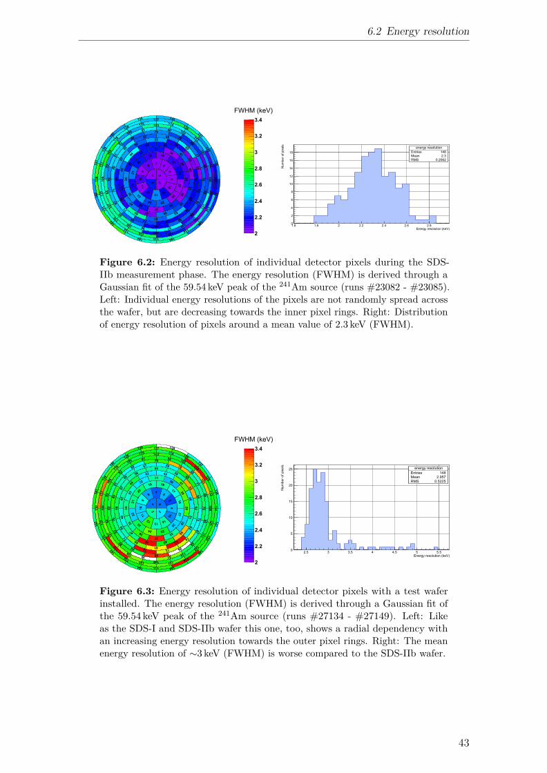
6.2 Energy resolution
2
2.2
2.4
2.6
2.8
3
3.2
3.4
01
2 3
45
678
910
11
12 1314
15
16
17
1819
20
2122
23
24 25
26
27
28
29
3031
32
3334
35
3637
38
39
40
41
4243
44
4546
47
48 49
50
51
52
53
54
55
56
57
58
59
60
61
62
63
64
65
6667
68
6970
71
72 73
74
75
76
77
78
79
80
81
82
83
84
85
86
87
88
89
9091
92
9394
95
96 97
98
99
100
101
102
103
104
105
106
107
108
109
110
111
112
113
114115
116
117
118
119
120 121
122
123
124
125
126
127
128
129
130
131
132
133
134
135
136
137
138139
140
141
142
143
144 145
146
147
FWHM (keV)
EnergyresolutionEntries 148Mean 2.3RMS 0.2062
Energy resolution (keV)1.6 1.8 2 2.2 2.4 2.6 2.8
Num
ber
ofpi
xels
0
2
4
6
8
10
12
14
16
18
energy resolutionEntries 148Mean 2.3RMS 0.2062
Figure 6.2: Energy resolution of individual detector pixels during the SDS-IIb measurement phase. The energy resolution (FWHM) is derived through aGaussian fit of the 59.54 keV peak of the 241Am source (runs #23082 - #23085).Left: Individual energy resolutions of the pixels are not randomly spread acrossthe wafer, but are decreasing towards the inner pixel rings. Right: Distributionof energy resolution of pixels around a mean value of 2.3 keV (FWHM).
2
2.2
2.4
2.6
2.8
3
3.2
3.4
01
2 3
45
678
910
11
12 1314
15
16
17
1819
20
2122
23
24 25
26
27
28
29
3031
32
3334
35
3637
38
39
40
41
4243
44
4546
47
48 49
50
51
52
53
54
55
56
57
58
59
60
61
62
63
64
65
6667
68
6970
71
72 73
74
75
76
77
78
79
80
81
82
83
84
85
86
87
88
89
9091
92
9394
95
96 97
98
99
100
101
102
103
104
105
106
107
108
109
110
111
112
113
114115
116
117
118
119
120 121
122
123
124
125
126
127
128
129
130
131
132
133
134
135
136
137
138139
140
141
142
143
144 145
146
147
FWHM (keV)
EnergyresolutionEntries 148Mean 2.957RMS 0.5225
Energy resolution (keV)2.5 3 3.5 4 4.5 5 5.5
Num
ber
ofpi
xels
0
5
10
15
20
25 energy resolutionEntries 148Mean 2.957RMS 0.5225
Figure 6.3: Energy resolution of individual detector pixels with a test waferinstalled. The energy resolution (FWHM) is derived through a Gaussian fit ofthe 59.54 keV peak of the 241Am source (runs #27134 - #27149). Left: Likeas the SDS-I and SDS-IIb wafer this one, too, shows a radial dependency withan increasing energy resolution towards the outer pixel rings. Right: The meanenergy resolution of ∼3 keV (FWHM) is worse compared to the SDS-IIb wafer.
43
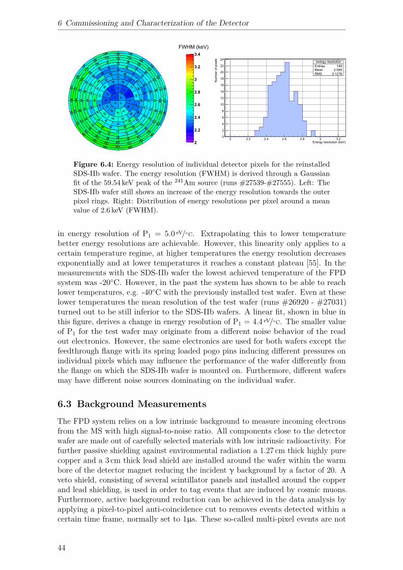
6 Commissioning and Characterization of the Detector
EnergyresolutionEntries 148Mean 2.589RMS 0.1278
Energy resolution HkeV)2 2.2 2.4 2.6 2.8 3 3.2
Num
ber
ofpi
xels
0
2
4
6
8
10
12
14
16
18
20
22
24energy resolution
Entries 148Mean 2.589RMS 0.1278
2
2.2
2.4
2.6
2.8
3
3.2
3.4
01
2 3
45
678
910
11
12 1314
15
16
17
1819
20
2122
23
24 25
26
27
28
29
3031
32
3334
35
3637
38
39
40
41
4243
44
4546
47
48 49
50
51
52
53
54
55
56
57
58
59
60
61
62
63
64
65
6667
68
6970
71
72 73
74
75
76
77
78
79
80
81
82
83
84
85
86
87
88
89
9091
92
9394
95
96 97
98
99
100
101
102
103
104
105
106
107
108
109
110
111
112
113
114115
116
117
118
119
120 121
122
123
124
125
126
127
128
129
130
131
132
133
134
135
136
137
138139
140
141
142
143
144 145
146
147
FWHM HkeV)
Figure 6.4: Energy resolution of individual detector pixels for the reinstalledSDS-IIb wafer. The energy resolution (FWHM) is derived through a Gaussianfit of the 59.54 keV peak of the 241Am source (runs #27539-#27555). Left: TheSDS-IIb wafer still shows an increase of the energy resolution towards the outerpixel rings. Right: Distribution of energy resolutions per pixel around a meanvalue of 2.6 keV (FWHM).
in energy resolution of P1 = 5.0 eV/C. Extrapolating this to lower temperaturebetter energy resolutions are achievable. However, this linearity only applies to acertain temperature regime, at higher temperatures the energy resolution decreasesexponentially and at lower temperatures it reaches a constant plateau [55]. In themeasurements with the SDS-IIb wafer the lowest achieved temperature of the FPDsystem was -20C. However, in the past the system has shown to be able to reachlower temperatures, e.g. -40C with the previously installed test wafer. Even at theselower temperatures the mean resolution of the test wafer (runs #26920 - #27031)turned out to be still inferior to the SDS-IIb wafers. A linear fit, shown in blue inthis figure, derives a change in energy resolution of P1 = 4.4 eV/C. The smaller valueof P1 for the test wafer may originate from a different noise behavior of the readout electronics. However, the same electronics are used for both wafers except thefeedthrough flange with its spring loaded pogo pins inducing different pressures onindividual pixels which may influence the performance of the wafer differently fromthe flange on which the SDS-IIb wafer is mounted on. Furthermore, different wafersmay have different noise sources dominating on the individual wafer.
6.3 Background Measurements
The FPD system relies on a low intrinsic background to measure incoming electronsfrom the MS with high signal-to-noise ratio. All components close to the detectorwafer are made out of carefully selected materials with low intrinsic radioactivity. Forfurther passive shielding against environmental radiation a 1.27 cm thick highly purecopper and a 3 cm thick lead shield are installed around the wafer within the warmbore of the detector magnet reducing the incident γ background by a factor of 20. Aveto shield, consisting of several scintillator panels and installed around the copperand lead shielding, is used in order to tag events that are induced by cosmic muons.Furthermore, active background reduction can be achieved in the data analysis byapplying a pixel-to-pixel anti-coincidence cut to removes events detected within acertain time frame, normally set to 1µs. These so-called multi-pixel events are not
44
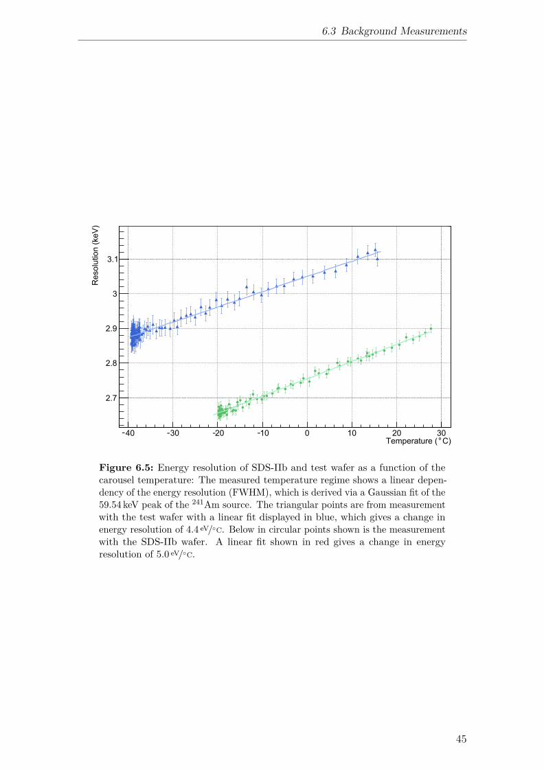
6.3 Background Measurements
C)Temperature (40 30 20 10 0 10 20 30
Res
olut
ion
(keV
)
2.7
2.8
2.9
3
3.1
°- - - -
Figure 6.5: Energy resolution of SDS-IIb and test wafer as a function of thecarousel temperature: The measured temperature regime shows a linear depen-dency of the energy resolution (FWHM), which is derived via a Gaussian fit of the59.54 keV peak of the 241Am source. The triangular points are from measurementwith the test wafer with a linear fit displayed in blue, which gives a change inenergy resolution of 4.4 eV/C. Below in circular points shown is the measurementwith the SDS-IIb wafer. A linear fit shown in red gives a change in energyresolution of 5.0 eV/C.
45
6 Commissioning and Characterization of the Detector
necessarily detected on the same or adjacent pixel but can be distributed across thewafer, e.g. from cosmic rays or γs from radioactive decays passing through severalpixels on the wafer. Detailed analysis concerning this cut can be found in [55, 38].
For shifting the electron energy to a region with a more favorable background levelthe PAE can be put on (positive) HV. Additionally, this suppresses backscatteringeffects since with the increasing energy the incident angle of the electrons becomessmaller and backscattering is less probable. Changing the detector a magnet fieldallows to optimize the diameter of the relevant magnetic flux tube on the detectorand, thus, change the sensitive area on the wafer.
The measurements analyzed in this thesis were performed with the FPD systemmechanically separated from the main spectrometer. This means the detector isfacing the metal surface of the DN250 gate valve which occasionally emits low-energyelectrons due to through passing muons. With the PAE put on (positive) voltage theselow-energy electrons are accelerated towards the wafer which induces an additionalbackground. This is observable as multiple peaks of e · UPAE within the detectorbackground spectrum.
The detector background spectrumThe measured background spectrum is shown in figure 6.6. From 10 keV to lowerenergies a steep rise of the rate is observed which is due to the electronic noise edgebelow 6 keV. Between 6 and 10 keV several copper fluorescence lines induced by decayswithin the copper PAE appear as a region of elevated background. However, due tothe limited energy resolution of the detector individual lines can not be identified.Between 10 and 120 keV the background rate is dominated by fluorescence lightfrom surrounding materials encouraged by intrinsic radiation and cosmic rays. Therate decreases with a power law until the dominant background process changes atabout 120 keV. From there on most background is induced by cosmic muons passingthrough the wafer. These minimal-ionizing particles induce a characteristic landaudistributed background. Only a part of it is visible in the energy spectrum since atabout 180 keV all events go into overflow. Overflow occurs when the events exceedan upper acceptance signal height of the DAQ. It appears as a broad peak due tobaseline fluctuations of the individual channels [55, 50]. For the region of interest(ROI) for tritium β-electrons is between 15.6 keV to 20.6 keV with a background rateof 1.5 to 1.7mcps/keV.
As the background rate at higher energies is approximately the same for the differentwafers at different run times or settings, only the background rate between 0 keV and50 keV is shown in figure 6.7 and 6.8. The data taken with the SDS-IIb wafer duringSDS-IIb measurement phase is illustrated in blue, after reinstallation of this waferis shown in red, and the data taken with the test wafer is shown in green. Whileno significant change of the background rate was observed after reinstallation of theSDS-IIb wafer the rate is for both measurements in general lower compared to thetest wafers’. This may be due to the usage of a different feedthrough flange, the oneon which the test wafer is mounted has no cylindrical donut-shaped copper sleevesfor the pogo pins. These are installed in order to block internal radiation originatingfrom the individual feedthroughs to the preamplifiers (figure 4.6). Furthermore,this increased background rate between 9 keV and 14 keV of the test wafers’ data(green) may be due to an automatic threshold finder (implemented in ORCA) whichsets thresholds for every pixel separately. This can lead to a shifted noise edge for
46
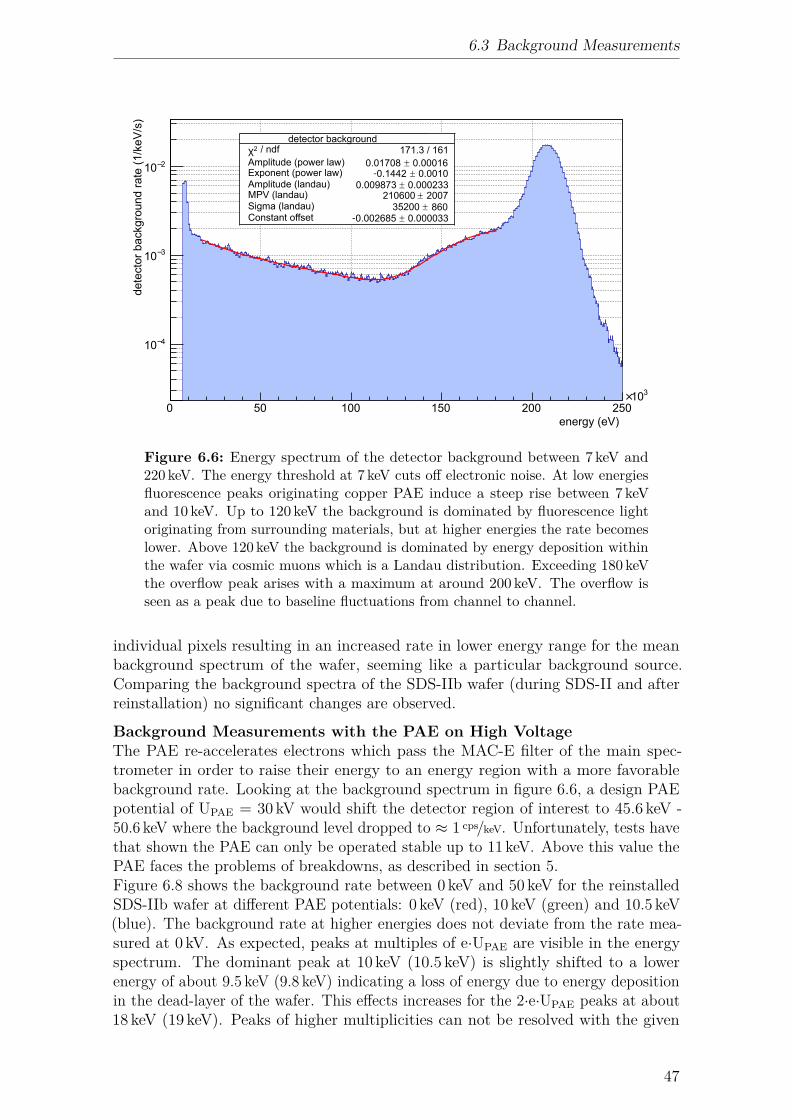
6.3 Background Measurements
0 50 100 150 200 250
310×
dete
ctor
back
grou
ndra
tef1
/keV
/sp
4−10
3−10
2−10
MultiPixelCutEntries 316785Mean 1.679em05RMS 6.622em04
/ ndf
2χ
171.3 / 161
p0 0.000160.01708p1 0.00100.1442−p2 0.0002330.009873p3 2.007em032.106em05p4 8.60em023.52em04p5 0.0000330.002685−
detector background/ ndf2χ 171.3 / 161
Amplitude fpower lawp 0.000160.01708Exponent fpower lawp 0.00100.1442Amplitude flandaup 0.0002330.009873MPV flandaup 2007210600Sigma flandaup 86035200Constant offset 0.0000330.002685-
-
energy feVp
Figure 6.6: Energy spectrum of the detector background between 7 keV and220 keV. The energy threshold at 7 keV cuts off electronic noise. At low energiesfluorescence peaks originating copper PAE induce a steep rise between 7 keVand 10 keV. Up to 120 keV the background is dominated by fluorescence lightoriginating from surrounding materials, but at higher energies the rate becomeslower. Above 120 keV the background is dominated by energy deposition withinthe wafer via cosmic muons which is a Landau distribution. Exceeding 180 keVthe overflow peak arises with a maximum at around 200 keV. The overflow isseen as a peak due to baseline fluctuations from channel to channel.
individual pixels resulting in an increased rate in lower energy range for the meanbackground spectrum of the wafer, seeming like a particular background source.Comparing the background spectra of the SDS-IIb wafer (during SDS-II and afterreinstallation) no significant changes are observed.
Background Measurements with the PAE on High VoltageThe PAE re-accelerates electrons which pass the MAC-E filter of the main spec-trometer in order to raise their energy to an energy region with a more favorablebackground rate. Looking at the background spectrum in figure 6.6, a design PAEpotential of UPAE = 30kV would shift the detector region of interest to 45.6 keV -50.6 keV where the background level dropped to ≈ 1 cps/keV. Unfortunately, tests havethat shown the PAE can only be operated stable up to 11 keV. Above this value thePAE faces the problems of breakdowns, as described in section 5.Figure 6.8 shows the background rate between 0 keV and 50 keV for the reinstalledSDS-IIb wafer at different PAE potentials: 0 keV (red), 10 keV (green) and 10.5 keV(blue). The background rate at higher energies does not deviate from the rate mea-sured at 0 kV. As expected, peaks at multiples of e·UPAE are visible in the energyspectrum. The dominant peak at 10 keV (10.5 keV) is slightly shifted to a lowerenergy of about 9.5 keV (9.8 keV) indicating a loss of energy due to energy depositionin the dead-layer of the wafer. This effects increases for the 2·e·UPAE peaks at about18 keV (19 keV). Peaks of higher multiplicities can not be resolved with the given
47
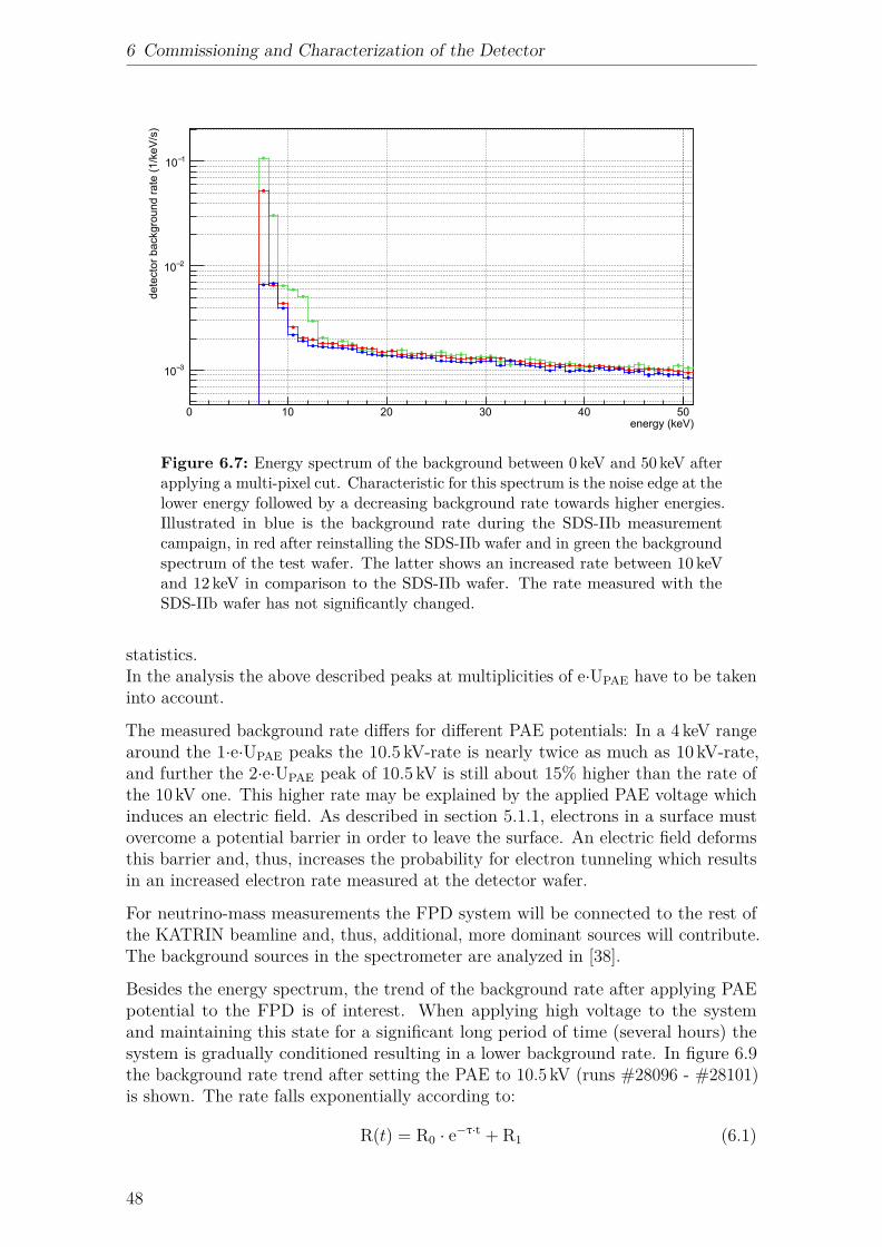
6 Commissioning and Characterization of the Detector
energy (keV)0 10 20 30 40 50
dete
ctor
back
grou
ndra
te(1
/keV
/s)
3−10
2−10
1−10
Figure 6.7: Energy spectrum of the background between 0 keV and 50 keV afterapplying a multi-pixel cut. Characteristic for this spectrum is the noise edge at thelower energy followed by a decreasing background rate towards higher energies.Illustrated in blue is the background rate during the SDS-IIb measurementcampaign, in red after reinstalling the SDS-IIb wafer and in green the backgroundspectrum of the test wafer. The latter shows an increased rate between 10 keVand 12 keV in comparison to the SDS-IIb wafer. The rate measured with theSDS-IIb wafer has not significantly changed.
statistics.In the analysis the above described peaks at multiplicities of e·UPAE have to be takeninto account.
The measured background rate differs for different PAE potentials: In a 4 keV rangearound the 1·e·UPAE peaks the 10.5 kV-rate is nearly twice as much as 10 kV-rate,and further the 2·e·UPAE peak of 10.5 kV is still about 15% higher than the rate ofthe 10 kV one. This higher rate may be explained by the applied PAE voltage whichinduces an electric field. As described in section 5.1.1, electrons in a surface mustovercome a potential barrier in order to leave the surface. An electric field deformsthis barrier and, thus, increases the probability for electron tunneling which resultsin an increased electron rate measured at the detector wafer.
For neutrino-mass measurements the FPD system will be connected to the rest ofthe KATRIN beamline and, thus, additional, more dominant sources will contribute.The background sources in the spectrometer are analyzed in [38].
Besides the energy spectrum, the trend of the background rate after applying PAEpotential to the FPD is of interest. When applying high voltage to the systemand maintaining this state for a significant long period of time (several hours) thesystem is gradually conditioned resulting in a lower background rate. In figure 6.9the background rate trend after setting the PAE to 10.5 kV (runs #28096 - #28101)is shown. The rate falls exponentially according to:
R(t) = R0 · e−τ·t + R1 (6.1)
48
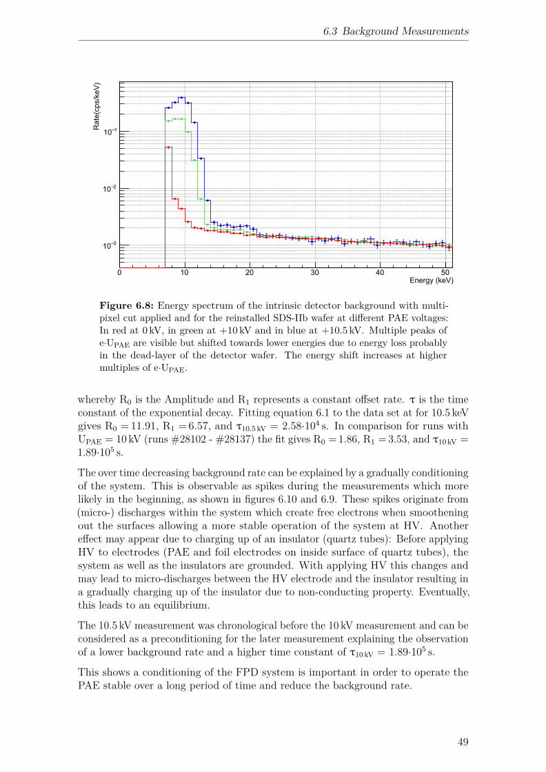
6.3 Background Measurements
Energy (keV)0 10 20 30 40 50
3−10
2−10
1−10
Rat
e(cp
s/ke
V)
Figure 6.8: Energy spectrum of the intrinsic detector background with multi-pixel cut applied and for the reinstalled SDS-IIb wafer at different PAE voltages:In red at 0 kV, in green at +10 kV and in blue at +10.5 kV. Multiple peaks ofe·UPAE are visible but shifted towards lower energies due to energy loss probablyin the dead-layer of the detector wafer. The energy shift increases at highermultiples of e·UPAE.
whereby R0 is the Amplitude and R1 represents a constant offset rate. τ is the timeconstant of the exponential decay. Fitting equation 6.1 to the data set at for 10.5 keVgives R0 = 11.91, R1 = 6.57, and τ10.5 kV = 2.58·104 s. In comparison for runs withUPAE = 10 kV (runs #28102 - #28137) the fit gives R0 = 1.86, R1 = 3.53, and τ10 kV =1.89·105 s.
The over time decreasing background rate can be explained by a gradually conditioningof the system. This is observable as spikes during the measurements which morelikely in the beginning, as shown in figures 6.10 and 6.9. These spikes originate from(micro-) discharges within the system which create free electrons when smootheningout the surfaces allowing a more stable operation of the system at HV. Anothereffect may appear due to charging up of an insulator (quartz tubes): Before applyingHV to electrodes (PAE and foil electrodes on inside surface of quartz tubes), thesystem as well as the insulators are grounded. With applying HV this changes andmay lead to micro-discharges between the HV electrode and the insulator resulting ina gradually charging up of the insulator due to non-conducting property. Eventually,this leads to an equilibrium.
The 10.5 kV measurement was chronological before the 10 kV measurement and can beconsidered as a preconditioning for the later measurement explaining the observationof a lower background rate and a higher time constant of τ10 kV = 1.89·105 s.
This shows a conditioning of the FPD system is important in order to operate thePAE stable over a long period of time and reduce the background rate.
49
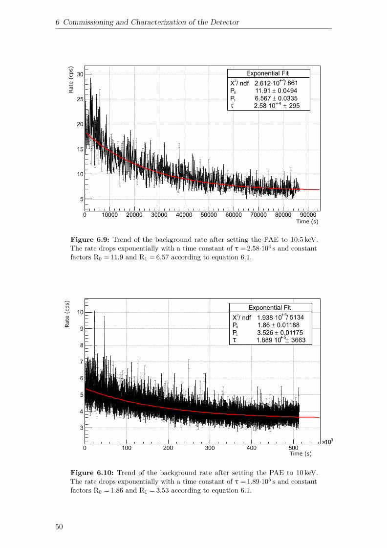
6 Commissioning and Characterization of the Detector
0 10000 20000 30000 40000 50000 60000 70000 80000 90000
5
10
15
20
25
30Rate(cps)
Time (s)
EnergyresolutionEntries 148Mean 2.589RMS 0.1278
Exponential Fit
XX/ ndf 2.612 10P 11.91 0.0494P 6.567 0.0335
2
1
0
. +4/ 861
2952.58 10+4
Figure 6.9: Trend of the background rate after setting the PAE to 10.5 keV.The rate drops exponentially with a time constant of τ = 2.58·104 s and constantfactors R0 = 11.9 and R1 = 6.57 according to equation 6.1.
0 100 200 300 400 500
310×
3
4
5
6
7
8
9
10
Time (s)
Rate(cps)
EnergyresolutionEntries 148Mean 2.589RMS 0.1278
Exponential Fit
XX/ ndf 1.938 10P 1.86 0.01188P 3.526 0.01175
2
1
0
. +4/ 5134
36631.889 10+5
Figure 6.10: Trend of the background rate after setting the PAE to 10 keV.The rate drops exponentially with a time constant of τ = 1.89·105 s and constantfactors R0 = 1.86 and R1 = 3.53 according to equation 6.1.
50
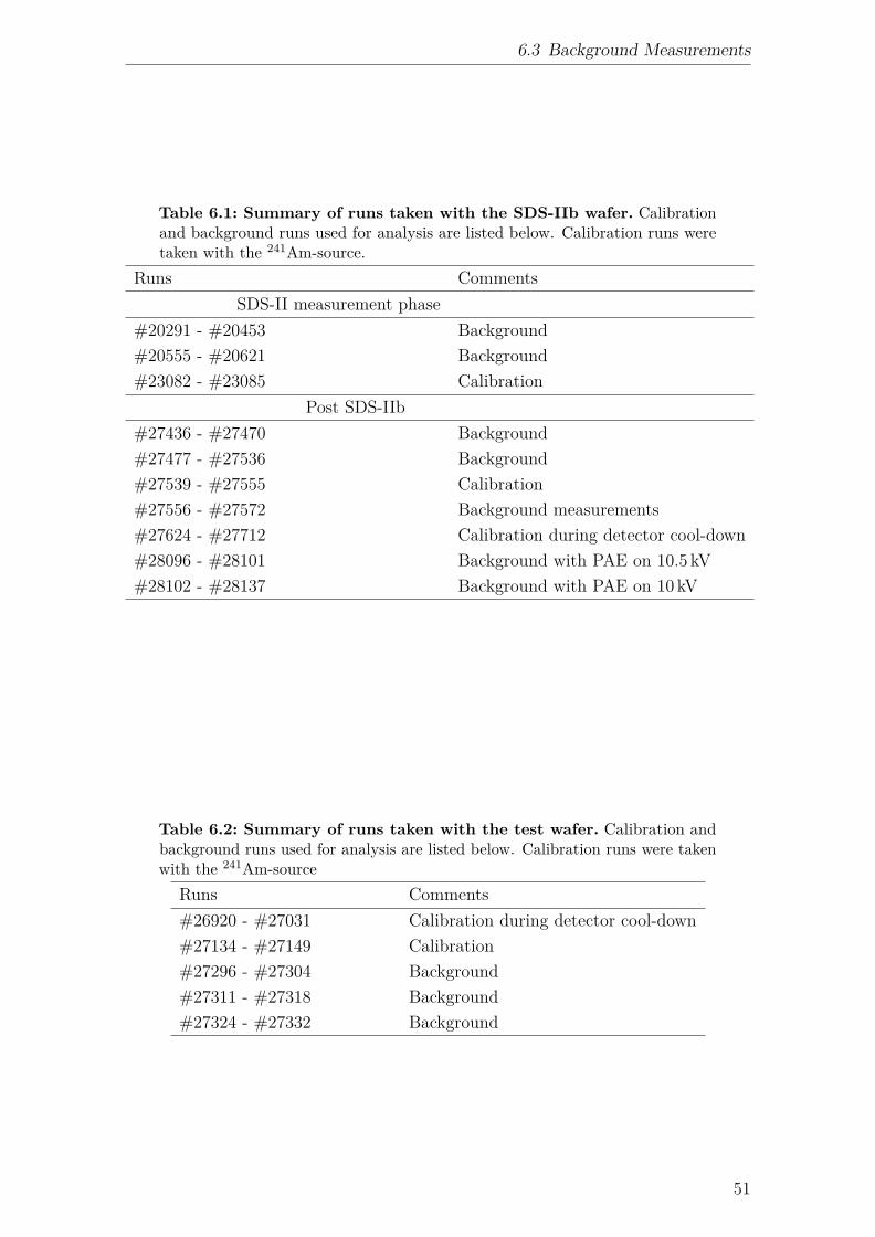
6.3 Background Measurements
Table 6.1: Summary of runs taken with the SDS-IIb wafer. Calibrationand background runs used for analysis are listed below. Calibration runs weretaken with the 241Am-source.
Runs CommentsSDS-II measurement phase
#20291 - #20453 Background#20555 - #20621 Background#23082 - #23085 Calibration
Post SDS-IIb#27436 - #27470 Background#27477 - #27536 Background#27539 - #27555 Calibration#27556 - #27572 Background measurements#27624 - #27712 Calibration during detector cool-down#28096 - #28101 Background with PAE on 10.5 kV#28102 - #28137 Background with PAE on 10 kV
Table 6.2: Summary of runs taken with the test wafer. Calibration andbackground runs used for analysis are listed below. Calibration runs were takenwith the 241Am-source
Runs Comments#26920 - #27031 Calibration during detector cool-down#27134 - #27149 Calibration#27296 - #27304 Background#27311 - #27318 Background#27324 - #27332 Background
51

7. Conclusions
The KArlsruhe TRItium Neutrino (KATRIN) experiment aims to determine the massof the electron anti-neutrino model independently with an unsurpassed sensitivityof mνe ≤ 200meV/c2 (90% C.L.). To achieve this goal, the kinetic energy of electronsfrom tritium β-decay is measured with high precision close to the endpoint energyE0. For this purpose KATRIN uses electrostatic retarding spectrometers basedon the MAC-E filter principle which allow to scan the β-spectrum in an integralway. Since only a small fraction of all electrons will pass the analyzing plane ofthe experiments main-spectrometer a detector with high detection efficiency anda low intrinsic background level is needed. These requirements are fulfilled by theFocal-Plane Detector (FPD) system of KATRIN which is based on a silicon PIN-diodedetector wafer. This wafer is circularly segmented in 148 pixels arranged in 12 rings(each with 12 pixels) around four Bulls-eye pixels in the center.
The objectives of this thesis were performance tests of two different wafers withregard to their spatial and energy resolution as well as their impact on the intrinsicdetector background. Furthermore, a separate test stand was set up together withthe KATRIN collaboration partners of the University of Washington, Seattle, inorder to improve the performance of a post-acceleration electrode (PAE) which isinstalled inside the FPD system and is used to boost the kinetic energy of signalelectrons to regimes of low intrinsic detector background.
In the first measurement campaign of the main spectrometer and detector section(SDS-I) in 2013 the used detector wafer showed a satisfying performance with a meanenergy resolution of 1.5 keV, but due to two shorted pixels its spatial resolution waslimited. For the subsequent measurement campaign SDS-II another detector waferwas installed into the FPD system. However, this wafer turned out to be inferior tothe SDS-I one with an energy resolution 2.3 keV. Nevertheless, the SDS-II wafer waschosen to be kept installed due to the advantage of 100% functioning pixels. A thirdwafer (test wafer), tested in between SDS-II and the upcoming SDS-III phase, hadan even worse energy resolution of about 3 keV while still providing 100% functioningpixels. After reinstalling the SDS-II wafer a degradation of its energy resolution to2.6 keV was discovered. In order to exclude the readout and amplification devices ofthe detector as cause of the observed degradation a series of test measurements werecarried out. These showed no influence of the electronics on the energy resolution,leaving the wafer itself as remaining candidate for the performance loss over time.The cause of this degradation trend is yet still unknown. However, the variety ofenergy resolutions for the different wafers can be explained by different qualities ofdifferent batches of wafers.Via an analysis of the single-pixel energy resolutions the spatial resolution of the
53
7 Conclusions
different detector wafers was investigated. For all four wafers tested in the past fewyears, a tendency showing an improvement of the single-pixel energy resolutionstowards inner pixel rings is observed. This may have several explanations: Firstly,the bias ring, used for biasing the detector wafer from its backside, may have aninfluence on the outer pixel rings despite a 2mm thick guard ring. Secondly, itis to be mentioned that the pressure on the detector wafer induced by the signalfeedthrough pins might influence the individual pixels, but previous investigationscould exclude this explanation for the most part. As it is a semiconductor, theperformance of the detector wafer is highly temperature dependent. Measurementstaken in a temperature range of -38C to +28C showed a linear relation betweenthe mean energy resolution and the temperature. However, for lower temperaturesthe energy resolution reaches a constant plateau and for higher temperatures itdegrades exponentially. This is explainable by thermal noise as well as leakagecurrent becoming more dominant at higher temperatures.
Besides the energy resolution one key parameter characterizing the detector perfor-mance is the intrinsic detector background spectrum. Comparing the backgroundspectra of the test wafer and SDS-II wafer show similar background rates above 30 keV.In the lower energy range close to the noise edge, however, the measured backgroundrates differ. This is most likely due to per-channel thresholds which are automaticallydetermined by the data acquisition (DAQ) software. Furthermore, a contribution tothe background can also originate from the different feedthrough flanges used. Indifference to the test wafer the flange on which the SDS-II wafer was mounted hadcopper sleeves around each signal feedthrough pin installed. These sleeves are used toshield the wafer from radiation originating from the feedthrough flange. Regardingthe region of interest for tritium measurements (15.6 keV to 30.6 keV) the backgroundrate is between 1.5 − 1.7mcps/keV.Applying high voltage to the PAE allows to shift the region of interest (ROI) to anenergy range with a more favorable background rate. By applying a voltage of 10 kV(10.5 kV) the ROI is shifted to 25.6 keV − 30.6 keV (26.1 keV − 21.1 keV) which anaverage background rate of 1mcps/keV improving the signal-to-noise ratio.The background rate trend measured directly after applying high voltage shows agradual reduction over a long period of time (several hours). This behavior may beexplained by a gradually conditioning of the system, a hypothesis further supportedby the observation of small spikes in the rate trend which appear less frequent withincreasing measurement time. These spikes can be attributed to (micro-) dischargeswithin the system temporarily increasing the measured background rate. Such dis-charges smoothen out the surfaces which allows a more stable operation of the systemat high voltage.
To this point it is not possible to operate the PAE at voltages higher than 11 kV.A separate test stand was build which is located at the University of Washington,Seattle, to test the PAE without risking damage to the sensitive electronics used inthe real system. The test stand uses vacuum chamber without the readout electronics,custom made parts (observation window and blanking flange) and has no magneticfield. The latter is possible because the occurrence of breakdowns is independent frommagnetic fields. A custom made blanking flange turned out not to be vacuum suitablewhich limits the achievable vacuum pressure to the 10−3 mbar regime. Vacuum testwere carried out to visually observe discharge processes within the PAE chamberfor the first time. The observations confirmed the results of previously carried out
54

simulation indicating regions of high electric field inside the PAE chamber. However,more tests at lower vacuum pressure, preferably in the same regime as at the FPD(10−6 mbar), are necessary for a better understanding of the breakdown phenomena.The test stand as a starting point for further developments may lead a more effectivemethod to condition the FPD system without harming sensitive read-out electronics.
55

56

Bibliography
[1] J. Chadwick, “Intensitätsverteilung im magnetischen spektrum der β-strahlenvon radium b+c,” Verhanlungenden Deutschen Physikalischen Gesellschaft,vol. 16, no. 1, pp. 383 – 391, 1914.
[2] W. Pauli, R. Kronig, and V. Weisskopf, Collected scientific papers. New York,NY: Interscience, 1964, offener Brief an die Gruppe der Radioaktiven bei derGauvereinstagung zu Tübingen (datiert 4. Dez. 1930).
[3] J. Chadwick, “The existence of a neutron,” in Proceedings of the Royal Societyof London A: Mathematical, Physical and Engineering Sciences, vol. 136, no.830. The Royal Society, 1932, pp. 692–708.
[4] E. Fermi, “Versuch einer theorie der β-Strahlen.” Zeitschrift für Physik, vol. 88,no. 3–4, pp. 161–177, 1934.
[5] H. Bethe and R. Peierls, “The’neutrino’,” Nature, vol. 133, no. 3362, p. 532,1934.
[6] F. Reines and C. L. Cowan, “The neutrino,” Nature, vol. 178, no. 4531, pp.446–449, 1956.
[7] G. Danby et al., “Observation of high-energy neutrino reactions and the existenceof two kinds of neutrinos,” Physical Review Letters, vol. 9, no. 1, p. 36, 1962.
[8] M. L. Perl et al., “Evidence for anomalous lepton production in e+- e- annihila-tion,” Physical Review Letters, vol. 35, no. 22, p. 1489, 1975.
[9] P. W. Higgs, “Broken symmetries and the masses of gauge bosons,” PhysicalReview Letters, vol. 13, no. 16, p. 508, 1964.
[10] C. ALEPH, DELPHI, L3, OPAL, SLD, L. E. W. Group et al., “Precisionelectroweak measurements on the z resonance,” arXiv preprint hep-ex/0509008,2005.
[11] B. Pontecorvo, “Inverse beta processes and nonconservation of lepton charge,”Zhur. Eksptl’. i Teoret. Fiz., vol. 34, 1958.
[12] J. N. Bahcall, “Solar neutrino cross sections and nuclear beta decay,”Phys. Rev., vol. 135, pp. B137–B146, Jul 1964. [Online]. Available:http://link.aps.org/doi/10.1103/PhysRev.135.B137
[13] R. Davis Jr, D. S. Harmer, and K. C. Hoffman, “Search for neutrinos from thesun,” Physical Review Letters, vol. 20, no. 21, p. 1205, 1968.
[14] J. N. Bahcall and R. Davis, “Solar Neutrinos - a Scientific Puzzle,” Science, vol.191, pp. 264–267, 1976.
57
BIBLIOGRAPHY
[15] W. Hampel, J. Handt, G. Heusser et al., “GALLEX solar neutrino observations:results for GALLEX IV,” Physics Letters B, vol. 447, no. 1–2, pp. 127 – 133,1999. [Online]. Available: http://www.sciencedirect.com/science/article/pii/S0370269398015792
[16] M. Altmann, M. Balata, P. Belli et al., “Complete results for fiveyears of GNO solar neutrino observations,” Physics Letters B, vol.616, no. 3–4, pp. 174 – 190, 2005. [Online]. Available: http://www.sciencedirect.com/science/article/pii/S0370269305005149
[17] J. N. Bahcall, “Solar neutrinos. i. theoretical,” Phys. Rev. Lett., vol. 12,pp. 300–302, Mar 1964. [Online]. Available: http://link.aps.org/doi/10.1103/PhysRevLett.12.300
[18] B. Pontecorvo, “Neutrino Experiments and the Problem of Conservation ofLeptonic Charge,” Sov. Phys. JETP, vol. 26, pp. 984–988, 1968, [Zh. Eksp.Teor. Fiz.53,1717(1967)].
[19] R. Helmer, “First results from the sudbury neutrino observatory,” NuclearPhysics B - Proceedings Supplements, vol. 111, no. 1, pp. 122 – 127,2002. [Online]. Available: http://www.sciencedirect.com/science/article/pii/S0920563202016936
[20] A. Bellerive, J. Klein, A. McDonald, A. Noble, and A. Poon, “The sudburyneutrino observatory,” Nuclear Physics B, vol. 908, pp. 30 – 51, 2016, neutrinoOscillations: Celebrating the Nobel Prize in Physics 2015. [Online]. Available:http://www.sciencedirect.com/science/article/pii/S0550321316300736
[21] B. Pontecorvo, “Inverse beta processes and nonconservation of lepton charge,”Sov. Phys. JETP, vol. 7, pp. 172–173, 1958, [Zh. Eksp. Teor. Fiz.34,247(1957)].
[22] Z. Maki, M. Nakagawa, and S. Sakata, “Remarks on the Unified Model ofElementary Particles,” Progress of Theoretical Physics, vol. 28, pp. 870–880,Nov. 1962.
[23] S. P. Mikheev and A. Yu. Smirnov, “Resonant amplification of neutrinooscillations in matter and solar neutrino spectroscopy,” Nuovo Cim., vol. C9,pp. 17–26, 1986.
[24] Y. Fukuda et al., “The Super-Kamiokande detector,” Nucl. Instrum. Meth., vol.A501, pp. 418–462, 2003.
[25] T. Gaisser and F. Halzen, “Icecube,” Annual Review of Nuclear andParticle Science, vol. 64, no. 1, pp. 101–123, 2014. [Online]. Available:http://dx.doi.org/10.1146/annurev-nucl-102313-025321
[26] S. F. King and C. Luhn, “Neutrino Mass and Mixing with Discrete Symmetry,”Rept. Prog. Phys., vol. 76, p. 056201, 2013.
[27] J. Lesgourgues and S. Pastor, “Neutrino cosmology and Planck,” New J. Phys.,vol. 16, p. 065002, 2014.
[28] M. Agostini et al., “Results on Neutrinoless Double-β Decay of 76Ge from PhaseI of the GERDA Experiment,” Phys. Rev. Lett., vol. 111, no. 12, p. 122503,2013.
58
BIBLIOGRAPHY
[29] D. G. Phillips, II et al., “The Majorana experiment: an ultra-low backgroundsearch for neutrinoless double-beta decay,” J. Phys. Conf. Ser., vol. 381, p.012044, 2012.
[30] M. Schlösser, “Accurate calibration of the raman system for the karlsruhe tritiumneutrino experiment,” Ph.D. dissertation, Karlsruher Institut für Technologie(KIT), 2013.
[31] S. R. Elliott and P. Vogel, “Double beta decay,” Annual Review of Nuclearand Particle Science, vol. 52, no. 1, pp. 115–151, 2002. [Online]. Available:http://dx.doi.org/10.1146/annurev.nucl.52.050102.090641
[32] P. A. M. Dirac, “The quantum theory of the emission and absorption ofradiation,” Proceedings of the Royal Society of London A: Mathematical, Physicaland Engineering Sciences, vol. 114, no. 767, pp. 243–265, 1927. [Online].Available: http://rspa.royalsocietypublishing.org/content/114/767/243
[33] H. Barth, A. Bleile, J. Bonn et al., “The status of the mainzneutrino mass experiment,” Nuclear Physics B - Proceedings Supplements,vol. 66, no. 1, pp. 183 – 186, 1998. [Online]. Available: http://www.sciencedirect.com/science/article/pii/S0920563298000310
[34] V. N. Aseev, A. I. Belesev, A. I. Berlev et al., “Measurement of the electronantineutrino mass in tritium beta decay in the Troitsk nu-mass experiment,”Physics of Atomic Nuclei, vol. 75, no. 4, pp. 464–478, 2012. [Online]. Available:http://dx.doi.org/10.1134/S1063778812030027
[35] K. Olive and P. D. Group, “Review of particle physics,” ChinesePhysics C, vol. 38, no. 9, p. 090001, 2014. [Online]. Available:http://stacks.iop.org/1674-1137/38/i=9/a=090001
[36] KATRIN collaboration, “KATRIN design report,” FZKA scientific report,vol. 7090, 2005. [Online]. Available: http://bibliothek.fzk.de/zb/berichte/FZKA7090.pdf
[37] J. Wolf, “The KATRIN neutrino mass experiment,” Nuclear Instrumentsand Methods in Physics Research Section A: Accelerators, Spectrometers,Detectors and Associated Equipment, vol. 623, no. 1, pp. 442 – 444, 2010,1st International Conference on Technology and Instrumentation in ParticlePhysics. [Online]. Available: http://www.sciencedirect.com/science/article/pii/S0168900210005942
[38] A. Müller, “Investigation of the secondary electron emission characteristicsof the KATRIN main spectrometer,” Master Thesis, Karlsruher Institut fürTechnologie (KIT), 2015. [Online]. Available: https://fuzzy.fzk.de/bscw/bscw.cgi/1043002?op=preview&back_url=15294%3fclient_size%3d1920x889
[39] N. Wandkowsky, “Study of background and transmission properties ofthe KATRIN spectrometers,” Ph.D. dissertation, Karlsruher Institut fürTechnologie (KIT), 2013. [Online]. Available: http://digbib.ubka.uni-karlsruhe.de/volltexte/1000036631
[40] S. Groh, “Modeling of the response function and measurement oftransmission properties of the KATRIN experiment,” Ph.D. dissertation,
59
BIBLIOGRAPHY
Karlsruher Institut für Technologie (KIT), 2015. [Online]. Available:http://nbn-resolving.org/urn:nbn:de:swb:90-465464
[41] S. Grohmann, T. Bode, H. Schön, and M. Süßer, “Precise temperature measure-ment at 30 k in the KATRIN source cryostat,” Cryogenics, vol. 51, no. 8, pp.438–445, 2011.
[42] T. B. Windberger, “Optimierung des 2-phasen-kühlkonzepts für den wgts-demonstrator von KATRIN,” Diploma Thesis, Karlsruher Institut für Technologie(KIT), 2011.
[43] S. Grohmann, T. Bode, M. Hötzel, H. Schön, M. Süßer, and T. Wahl, “Thethermal behaviour of the tritium source in KATRIN,” Cryogenics, vol. 55-56,no. 0, pp. 5–11, 2013.
[44] M. Schlösser, S. Fischer, M. Sturm, B. Bornschein, R. Lewis, and H. Telle,“Design implications for laser raman measurement systems for tritiumsample-analysis, accountancy or process-control applications,” Fusion Scienceand Technology, vol. 60, no. 3, pp. 976–981, 2011. [Online]. Available:http://www.ans.org/pubs/journals/fst/a_12579
[45] M. Sturm, “Bestimmung der tritiumflussreduktion einer tritium-argon-frostpumpe für das neutrinomassenexperiment KATRIN,” Diploma Thesis,Universität Karlsruhe (TH), 2007. [Online]. Available: http://www.katrin.kit.edu/publikationen/dth-sturm.pdf
[46] M. Ubieto Díaz, “Off-line commissioning of a non-destructive FT-ICRdetection system for monitoring the ion concentration in the KATRINbeamline,” Ph.D. dissertation, Ruperto-Carola University of Heidelberg,2011. [Online]. Available: http://pubman.mpdl.mpg.de/pubman/item/escidoc:1255588:2/component/escidoc:1255587/2Ubieto_Thesis.pdf
[47] M. Ubieto-Díaz, D. Rodríguez, S. Lukic, S. Nagy, S. Stahl, and K. Blaum, “Abroad-band FT-ICR penning trap system for KATRIN,” International Journalof Mass Spectrometry, vol. 288, no. 1–3, pp. 1–5, 2009.
[48] M. Hackenjos, “Die differentielle pumpstrecke des KATRIN-experiments -inbetriebnahme und charakterisierung des supraleitenden magnetsystems,”Master Thesis, Karlsruher Institut für Technologie (KIT), 2015. [Online].Available: http://www.katrin.kit.edu/publikationen/MaT_Hackenjos.pdf
[49] A. Windberger, “Berechnungen und simulationen zum verhalten von ionenin der differenziellen pumpstrecke des KATRIN-experiments,” DiplomaThesis, Karlsruher Institut für Technologie (KIT), 2011. [Online]. Available:http://www.katrin.kit.edu/publikationen/dth-windberger.pdf
[50] F. Harms, “Characterization and minimization of background processes inthe katrin main spectrometer,” Ph.D. dissertation, Karlsruher Institut fürTechnologie (KIT), 2015. [Online]. Available: http://nbn-resolving.org/urn:nbn:de:swb:90-500274
[51] W. Gil, J. Bonn, B. Bornschein, R. Gehring, O. Kazachenko, J. Kleinfeller, andS. Putselyk, “The Cryogenic Pumping Section of the KATRIN experiment,”IEEE Transactions on Applied Superconductivity, vol. 20, no. 3, pp. 316–319,2010.
60
BIBLIOGRAPHY
[52] R. Bottesch, “Set-up of the motion control and characterization of the ablationlaser for the condensed 83mKr conversion electron source of the KATRINexperiment,” Diploma Thesis, Westfälische Wilhelms-Universität Münster, 2012.[Online]. Available: http://www.uni-muenster.de/Physik.KP/AGWeinheimer/Files/theses/Diplom_Richard_Bottesch.pdf
[53] M. Prall, P. Renschler, F. Glück, A. Beglarian, H. Bichsel, L. Bornschein,Z. Chaoui, G. Drexlin, F. Fränkle, S. Görhardt, S. Mertens, M. Steidl, T. Thümm-ler, S. Wüstling, C. Weinheimer, and S. Zadorozhny, “The KATRIN pre-spectrometer at reduced filter energy,” New Journal of Physics, vol. 14, no. 7, p.073054, 2012.
[54] F. Glück, G. Drexlin, B. Leiber, S. Mertens, A. Osipowicz, J. Reich, andN. Wandkowsky, “Electromagnetic design of the large-volume air coil system ofthe KATRIN experiment,” New Journal of Physics, vol. 15, no. 8, p. 083025,2013.
[55] J. S. Schwarz, “The detector system of the KATRIN experiment -implementation and first measurements with the spectrometer,” Ph.D.dissertation, Karlsruher Institut für Technologie (KIT), 2014. [Online].Available: http://nbn-resolving.org/urn:nbn:de:swb:90-427724
[56] B. Leiber, “Investigations of background due to secondary electron emissionin the KATRIN-experiment,” Ph.D. dissertation, Karlsruher Institut fürTechnologie (KIT), 2014. [Online]. Available: http://nbn-resolving.org/urn:nbn:de:swb:90-424154
[57] J. Barrett, A. Beglarian, J. Behrens et al., “Results of the first KATRIN SDSmeasurement phase,” internal KATRIN document, 2014.
[58] F. R. Müller, “Efficiency studies of the background suppression bya liquid-nitrogen cooled baffle system in the katrin experiment,” Mas-ter Thesis, Karlsruher Institut für Technologie (KIT), 2015. [Online].Available: https://fuzzy.fzk.de/bscw/bscw.cgi/966078?op=preview&back_url=15294%3fclient_size%3d1920x889
[59] F. Bandenburg, “Inbetriebnahme des fokalebenendetektor-systems für eine zweitemessphase am KATRIN-hauptspektrometer,” Diploma Thesis, Karlsruher Insti-tut für Technologie (KIT), 2014.
[60] E. L. Martin, “FPD wafer test board,” internal KATRIN document,2014. [Online]. Available: https://fuzzy.fzk.de/bscw/bscw.cgi/875187?op=preview&back_url=1005301
[61] S. Schmid, “Performance des fokalebenendetektors zu beginn der zweiten gemein-samen messphase mit dem KATRIN hauptspektrometer,” Bachelor Thesis, Karl-sruher Institut für Technologie (KIT), 2014.
[62] J. Amsbaugh, J. Barrett, A. Beglarian et al., “Focal-plane detector system for theKATRIN experiment,” Nuclear Instruments and Methods in Physics ResearchSection A: Accelerators, Spectrometers, Detectors and Associated Equipment,vol. 778, pp. 40–60, 2015.
[63] F. Harms, “Assembly and first results of the KATRIN focal-plane detectorsystem at KIT,” Diploma Thesis, Karlsruher Institut für Technologie (KIT),
61
BIBLIOGRAPHY
2012. [Online]. Available: http://www.katrin.kit.edu/publikationen/dth_Fabian_Harms.pdf
[64] J. F. Amsbaugh, N. M. Boyd, and D. M. S. Parno, “Runge-kutta method fornumerical solution of differential equation system,” internal KATRIN document,2012. [Online]. Available: https://fuzzy.fzk.de/bscw/bscw.cgi/1012705?op=preview&back_url=1005301
[65] C. Kittel, Einführung in die Festkörperphysik, 15th ed.München: Oldenbourg, 2013. [Online]. Avail-able: http://deposit.d-nb.de/cgi-bin/dokserv?id=4223635&prov=M&dok_var=1&dok_ext=htm;http://d-nb.info/1029368872/04
[66] B. VanDevender, L. Bodine, A. Myers et al., “Performance of a TiN-coatedmonolithic silicon pin-diode array under mechanical stress,” Nuclear Instru-ments and Methods in Physics Research Section A: Accelerators, Spectrometers,Detectors and Associated Equipment, vol. 673, no. 0, pp. 46–50, 2012.
[67] G. F. Knoll, Radiation detection and measurement; 4th ed. New York, NY:Wiley, 2010. [Online]. Available: https://cds.cern.ch/record/1300754
[68] Johannes and Sascha, “Feedthrough flange and wafer #96728 inspection,”2012. [Online]. Available: https://crunch5.npl.washington.edu:8443/KATRIN+Detector+Commissioning+/485
[69] F. Fränkle, “Visual inspection of wafer #115877,” 2016, main-detector, MessageID: 13. [Online]. Available: https://neutrino.ikp.kit.edu:8080/main-detector/13
[70] A. Seher, “Visual inspection of wafer #115875,” 2016, main-detector, MessageID: 16. [Online]. Available: https://neutrino.ikp.kit.edu:8080/main-detector/16
[71] V. T. Jordanov and G. F. Knoll, “Digital synthesis of pulse shapes in real timefor high resolution radiation spectroscopy,” Nuclear Instruments and Methodsin Physics Research Section A: Accelerators, Spectrometers, Detectors andAssociated Equipment, vol. 345, no. 2, pp. 337 – 345, 1994. [Online]. Available:http://www.sciencedirect.com/science/article/pii/0168900294910111
[72] J. Formaggio, “The KATRIN veto and shield system,” internal KATRIN docu-ment, 2007.
[73] J. D. Craggs and J. M. J. M. Meek, Electrical breakdown of gases, rev. ed ed.Chichester ; New York : Wiley, 1978, "A Wiley-Interscience publication.".
[74] V. A. Nevrovsky, V. I. Rakhovsky, and V. G. Zhurbenko, “Dc breakdown ofultra-high vacuum gaps,” Beiträge aus der Plasmaphysik, vol. 23, no. 4, pp.433–458, 1983. [Online]. Available: http://dx.doi.org/10.1002/ctpp.19830230410
[75] “Front matter,” in Physical Methods in Chemical Analysis, W. G.BERL, Ed. Academic Press, 1956, pp. iii –. [Online]. Available:http://www.sciencedirect.com/science/article/pii/B9781483232386500019
[76] F. Glück, “The penning discharge,” internal KATRIN document, 2007. [Online].Available: https://fuzzy.fzk.de/bscw/bscw.cgi/354775?op=preview&back_url=354761%3fclient_size%3d1920x920
62
BIBLIOGRAPHY
[77] F. Paschen, “Ueber die zum funkenübergang in luft, wasserstoff undkohlensäure bei verschiedenen drucken erforderliche potentialdifferenz,” Annalender Physik, vol. 273, no. 5, pp. 69–96, 1889. [Online]. Available:http://dx.doi.org/10.1002/andp.18892730505
[78] W. contributors, “Sensitivity of next-generation tritium beta-decay experimentsfor kev-scale sterile neutrinos,” Wikipedia, The Free Encyclopedia. [Online].Available: https://en.wikipedia.org/w/index.php?title=Microplasma&oldid=686991284
[79] F. M. Fränkle, “Background investigations of the KATRIN pre-spectrometer,”Ph.D. dissertation, Karlsruher Institut für Technologie (KIT), 2010. [Online].Available: http://nbn-resolving.org/urn:nbn:de:swb:90-193929
[80] S. Groh, “Untersuchung von uv-laser induziertem untergrund am KATRINvorspektrometer,” Diploma Thesis, Karlsruher Institut für Technologie (KIT),2010. [Online]. Available: http://www.katrin.kit.edu/publikationen/dth-groh.pdf
[81] A. Picard, H. Backe, H. Barth et al., “A solenoid retarding spectrometer withhigh resolution and transmission for kev electrons,” Nuclear Instruments andMethods in Physics Research Section B: Beam Interactions with Materials andAtoms, vol. 63, no. 3, pp. 345–358, 1992.
[82] F. Penning, “Die glimmentladung bei niedrigem druck zwischen koaxialenzylindern in einem axialen magnetfeld,” Physica, vol. 3, no. 9, pp. 873 – 894,1936. [Online]. Available: http://www.sciencedirect.com/science/article/pii/S0031891436803139
[83] F. Fränkle, F. Glück, K. Valerius et al., “Penning discharge in the KATRINpre-spectrometer,” Journal of Instrumentation, vol. 9, no. 7, p. P07028, 2014.
[84] A. Müller, “High voltage simulation of the PAE,” internal KATRIN document,2014.
63

Acknowledgments
Abschließend möchte ich mich an dieser Stelle ganz herzlich bei allen bedanken, diemich im letzten Jahr begleitet, unterstützt und zum Gelingen meiner Masterarbeitbeigetragen haben. Ein besonderer Dank gilt hierbei im Besonderen:
• Prof. Dr. Guido Drexlin für die Möglichkeit meine Masterabeit bei KATRINschreiben zu dürfen.
• Prof. Wim de Boer dafür, dass er freundlicherweise das Korreferat übernommenhat.
• Dr. Fabian Harms für die ausgezeichnete fachliche und persönliche Betreuung,sowie die vielen hilfreichen Tipps und Anregungen zu dieser Arbeit.
• Dr. Florian Fränkle für die zahlreichen und interessanten Diskussionen, diegroßartige Zusammenarbeit im Büro sowie am FPD System.
• Thank you Prof. Peter Doe and Prof. Diana Parno for giving me the oppor-tunity to stay at CENPA for several weeks and all other colleges from the UScollaboration partners, for their support and help during the assembly of thePAE test stand.
• Dr. Bianca Keilhauer, stellvertretend für das i-Progress Programm, für diefinanzielle Unterstützung während meines Aufenthalts in den USA.
• Allen Technikern, Doktoranden, Postdocs und weiteren beteiligten Personen,die uns bei der Wiederinbetriebnahme des FPD Systems unterstützt haben.
• Allen, die in diesem Jahr Kuchen mitgebracht, Pizza bestellt sowie geholt unddie Mittags- und Kaffeepausen bereichert haben.
Besonderen Dank gilt meinen Eltern und meinen Geschwistern, die mich währenddes Studiums immer unterstützt haben und Rückhalt gegeben haben. Im besonderenmöchte ich meinem Vater, Dieter H. E. Seher, danken, der mich bereits in früherKindheit den Naturwissenschaften nahe gebracht und zu diesem Studium ermutigthat, jedoch meinen Abschluss an dieser Stelle nicht mehr mit erleben durfte.
65