Embed Size (px)
Citation preview

CMOS Omnipolar High Sensitivity Micropower Hall Switch
1.Features
1
f
Micropower consumption for battery powered
applications
Omnipolar, output switches with absolute value o
North or South pole from magnet
Operation down to 2.5V
High sensitivity for direct reed switch
replacement applications
Chopper stabilized amplifier stage2.Description
IC is fabricated from mixed signal
CMOS technology .It incorporates advanced chopper-stabilization techniques to
provide accurate and stable magnetic switch points.
The circuit design provides an internally controlled clocking mechanism to
cycle power to the Hall element and analog signal processing circuits. This serves to
place the high current-consuming portions of the circuit into a “Sleep” mode.
Periodically the device is “Awakened” by this internal logic and the magnetic flux
from the Hall element is evaluated against the predefined thresholds. If the flux
density is above or below the Bop/Brp thresholds then the output transistor is driven
to change states accordingly. While in the “Sleep” cycle the output transistor is
latched in its previous state. The design has been optimized for service in
applications requiring extended operating
ill be latched on (Bop) in the presence
of a sufficiently strong South or North magnetic field facing the marked side of the
package. The output will be latched off (Brp) in the absence of a magnetic field.
The 248 Omnipolar Hall effect sensor
The output transistor of the 248 w
全极霍尔开关
型号:DH248
网址:http://www.hall-wafer.com
地址:深圳市龙岗区龙西清水路务地埔龙昌10楼1001
电话:0755-84821761 13430722511
3.Applications
Solid state switch
Handheld Wireless Handset Awake Switch
Lid close sensor for battery powered devices
Magnet proximity sensor for reed switch replacement in low duty cycle
applications
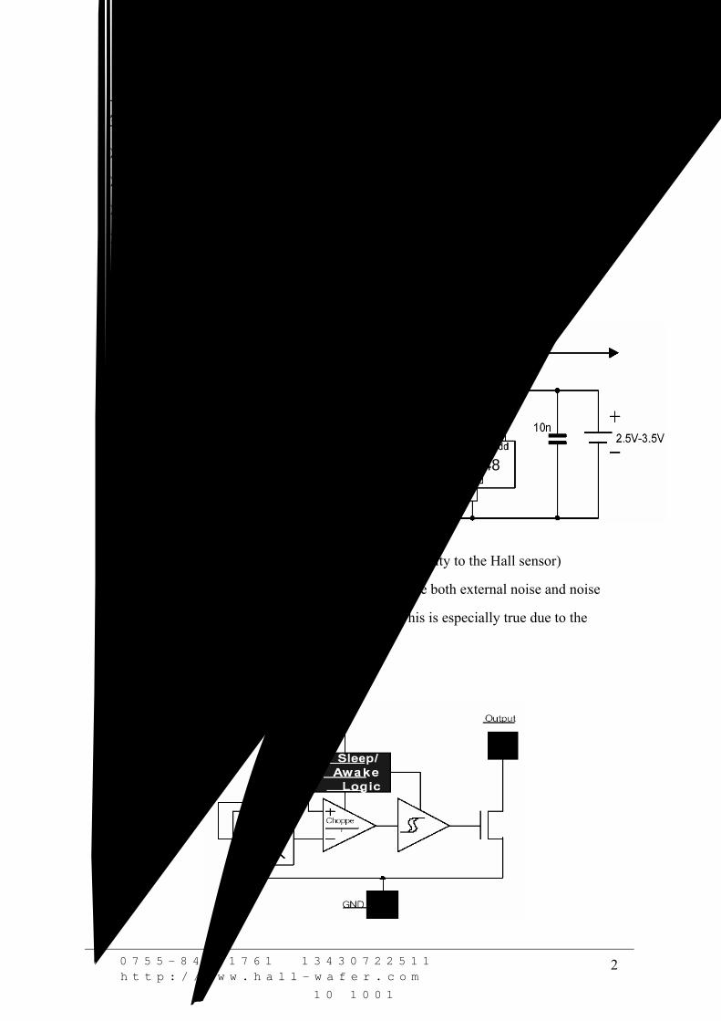
4.Typical Application Circuit
2
Eastera's pole-independent sensing
technique allows for operation with either a
north pole or south pole magnet orientation,
enhancing the manufacturability of the
device. The state-of-the-art technology
provides the same output polarity for either
pole face.
It is strongly recommended that an
external bypass capacitor be connected (in close proximity to the Hall sensor)
between the supply and ground of the device to reduce both external noise and noise
generated by the chopper-stabilization technique. This is especially true due to the
relatively high impedance of battery supplies.
EST
5.Functional Block Diagram
DH248
型号:DH248
网址:http://www.hall-wafer.com
地址:深圳市龙岗区龙西清水路务地埔龙昌10楼1001
电话:0755-84821761 13430722511
6.Pinning Mark View Pin Description
3
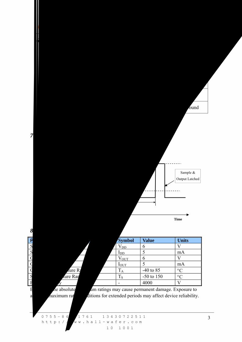
7.Internal Timing Circuit
8.Absolute Maximum Ratings
Parameter Symbol Value Units Supply Voltage(operating) VDD 6 V Supply Current IDD 5 mA Output Voltage VOUT 6 V Output Curent IOUT 5 mA Operating Temperature Range to 85 TA -40 °C Storage Temperature Rang to 150 TS -50 °C ESD Sensitivity - 4000 V Exceeding the absolute maximum ratings ma ause perm ge. Exposure to
m rated conditions for exten d periods ffect device reliability. y c anent dama
absolute-maximu de may a
NAME NO STATUS DESCRIPTION
Vdd 1 P Power Supply
Out 2 O output
Gnd 3 P IC Ground
Awake Taw:120μs
Period
Sleep Tsl:70ms
Time
Current
0
Isp
Iaw
Iav
Sample &
Output Latched
1
3
2
DH248
型号:DH248
网址:http://www.hall-wafer.com
地址:深圳市龙岗区龙西清水路务地埔龙昌10楼1001
电话:0755-84821761 13430722511
4
.DC Electrical Characteristics
DC Operating Parameters: TA = 25℃, VDD=2.75V.
9
Parameter Symbol Test Conditions Min Typ Max Units Operating voltage VDD Operating 2.5 3 5.5 V
Supply current IDD Average 5 μA Output Current IOUT 1.0 mA
S IOUT=1mA aturation Voltage VSAT 0.4 V Awake mode time TAW Operating 175 μS Sleep mode time TSL Operating mS
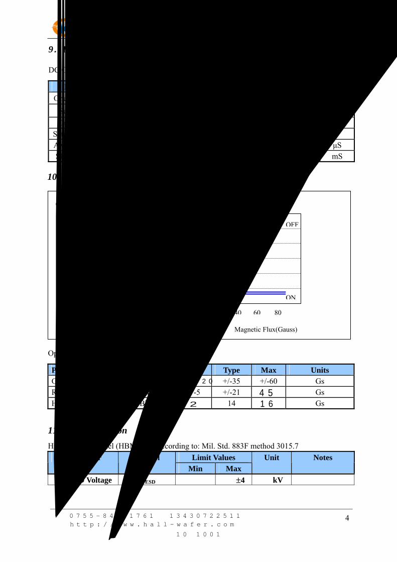
0.Magnetic Characteristics
Operating Parameters: TA = 25℃, VDD=2.75VDC.
1
PARAMETER Symbol Min Type Max Units Operating Point Bop +/-35 +/-60 Gs Release Point Brp +/-5 +/-21 Gs Hysteresis Bhys - 14 Gs
11.ESD Protection ) tests according to: Mil. Std. 883F method 3015.7 Human Body Model (HBM
Limit Values Parameter Symbol Min Max
Unit Notes
ESD Voltage VESD kV ±4
Output Voltage(V) 3.0
OFF2.5
2.0BOPN BRPS BOPS
1.5BRPN
1.0
0.5 ON
0-80 -60 -40 -20 0 20 40 60 80
Magnetic Flux(Gauss)
452 16
+/-20
型号:DH248
网址:http://www.hall-wafer.com
地址:深圳市龙岗区龙西清水路务地埔龙昌10楼1001
电话:0755-84821761 13430722511
120
5
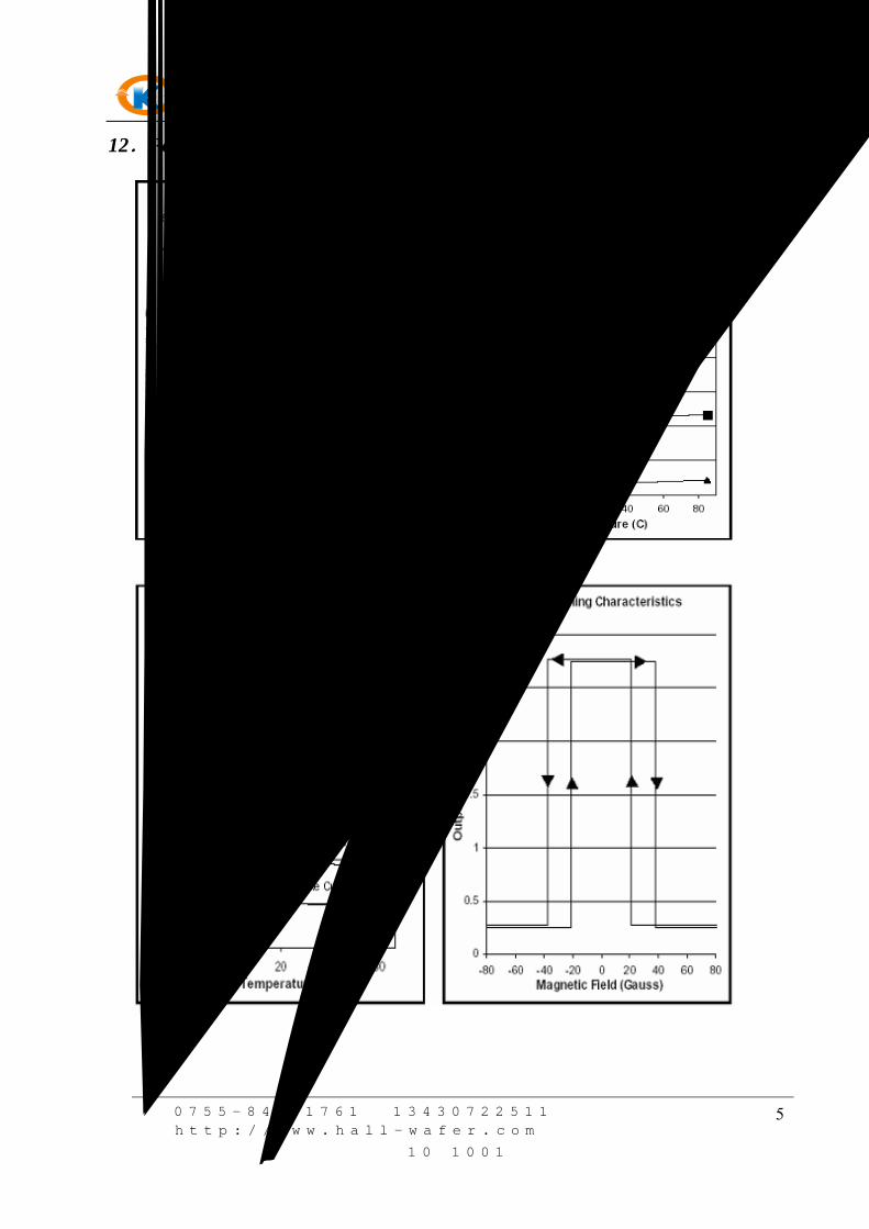
12.Performance Characteristics
型号:DH248
网址:http://www.hall-wafer.com
地址:深圳市龙岗区龙西清水路务地埔龙昌10楼1001
电话:0755-84821761 13430722511
13.Unique Features
CMOS Hall IC Technology
The chopper stabilized amplifier uses switched capacitor techniques to eliminate the
amplifier offset voltage, which, in bipolar devices, is a major source of temperature
sensitive drift. CMOS makes this advanced technique possible. The CMOS chip is also
much smaller than a bipolar chip, allowing very sophisticated circuitry to be placed in less
space. The small chip size also contributes to lower physical stress and less power
consumption.
Installation Comments
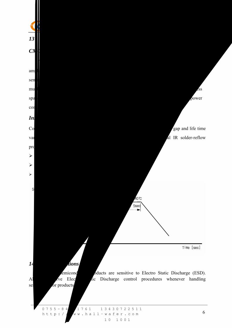
Consider temperature coefficients of Hall IC and magnetics , as well as air gap and life time
variations. Observe temperature limits during wave soldering. Typical IR solder-reflow
profile:
No Rapid Heating and Cooling.
Recommended Preheating for max. 2minutes at 150°C
Recommended Reflowing for max. 5seconds at 240°C
14.ESD Precautions Electronic semiconductor products are sensitive to Electro Static Discharge (ESD).
Always observe Electro Static Discharge control procedures whenever handling semiconductor products.
6
型号:DH248
网址:http://www.hall-wafer.com
地址:深圳市龙岗区龙西清水路务地埔龙昌10楼1001
电话:0755-84821761 13430722511
15.Package Information
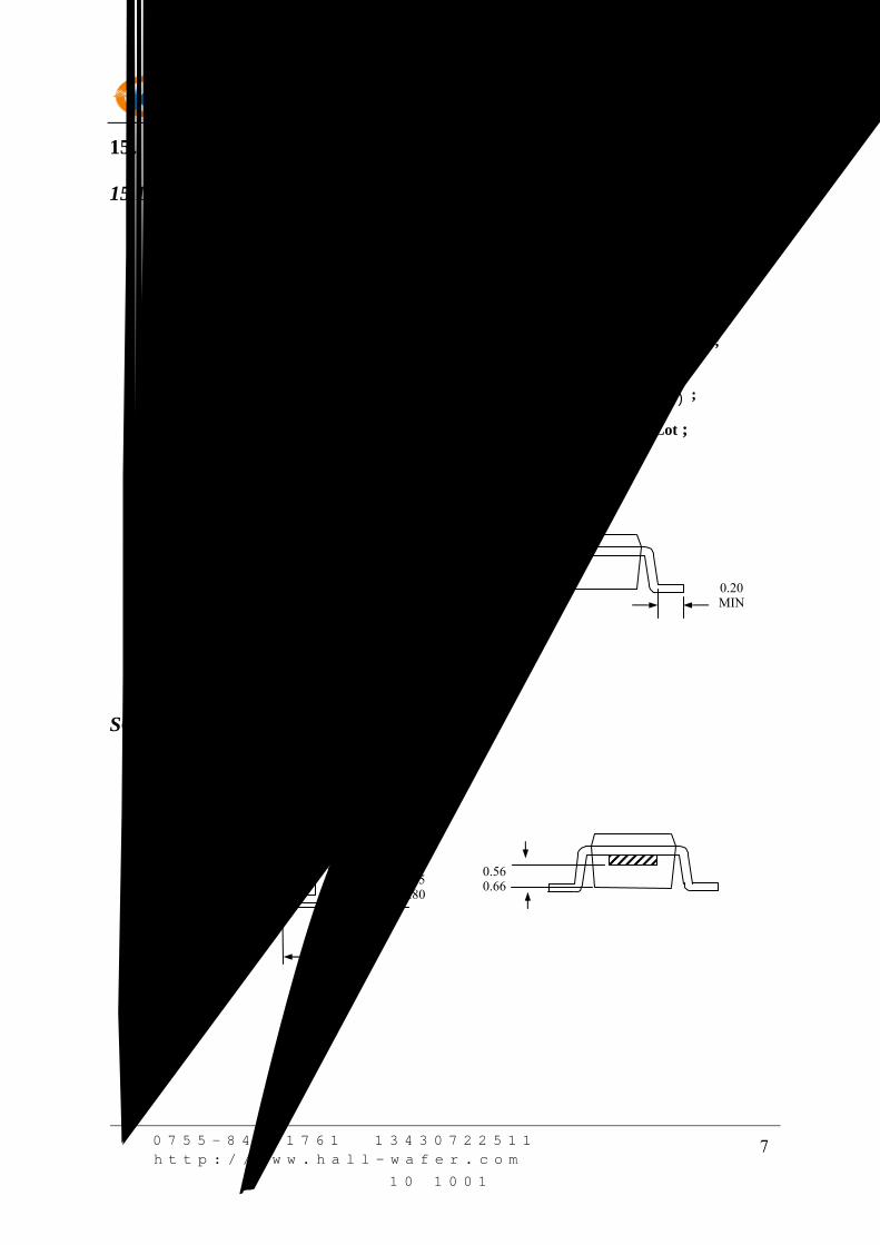
15.1 SOT-23 Package Physical Characteristics
2.70 3.10
1.001.300.70
0.90
0.000.10
0.35 0.50
0.100.25
0.20MIN
2.603.00
1.501.80
1.70 2.10
3
21
Top View
Side View End View
Notes: 1). PINOUT: Pin 1 VDD Pin 2 Output Pin 3 GND 2). All dimensions are in millimeters ; Marking:
; yy -- last 2 digit of year ; m -- “A”-“Z”, Production Lot ;
SOT-23 Package Hall Location
7
0.560.660.95
0.80
1.50 1.40
Chip 3
Bottom View of SOT-23 Package
2 1
48 -- Code of Device ( DH248 )
DH248
型号:DH248
网址:http://www.hall-wafer.com
地址:深圳市龙岗区龙西清水路务地埔龙昌10楼1001
电话:0755-84821761 13430722511
15.3 TO-92 Package Physical Characteristics
4.1 ± 0.1
1 2 3
1.27
2.13 1.87
1.001.20
45° ± 1°
1.58
± 0
.1
3° ± 1°
0.76
± 0
.05
3.18
± 0
.1
3 - 0.44
3 - 0.44
0.05 ± 0.05 2.3.
± 0.
1
0.84(Nom)
3° ± 1° 6° ± 1°
6° ± 1°3° ± 1°
14
± 0
.5 Notes:
1). Controlling dimension : mm ;
2). Lesds must be free of flash and plating voids ;
3). Do not bend leads within 1 mm of lead to package
interface ;
4). PINOUT: Pin 1 VDD
Pin 2 GND
Pin 3 Output
Active Area Depth:
Sensor Location
1 2 3
16. Ordering Information
DH248
型号:DH248
8
网址:http://www.hall-wafer.com
地址:深圳市龙岗区龙西清水路务地埔龙昌10楼1001
电话:0755-84821761 13430722511