Embed Size (px)
Citation preview
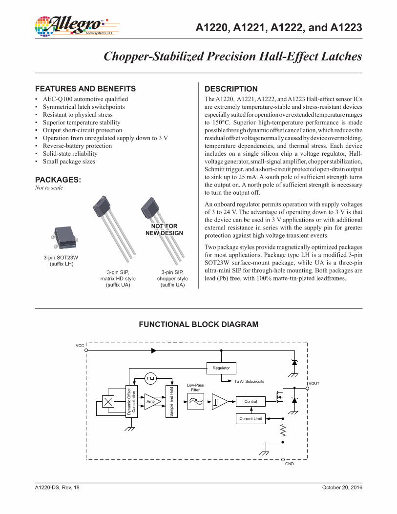
DESCRIPTIONThe A1220, A1221, A1222, and A1223 Hall-effect sensor ICs are extremely temperature-stable and stress-resistant devices especially suited for operation over extended temperature ranges to 150°C. Superior high-temperature performance is made possible through dynamic offset cancellation, which reduces the residual offset voltage normally caused by device overmolding, temperature dependencies, and thermal stress. Each device includes on a single silicon chip a voltage regulator, Hall-voltage generator, small-signal amplifier, chopper stabilization, Schmitt trigger, and a short-circuit protected open-drain output to sink up to 25 mA. A south pole of sufficient strength turns the output on. A north pole of sufficient strength is necessary to turn the output off.
An onboard regulator permits operation with supply voltages of 3 to 24 V. The advantage of operating down to 3 V is that the device can be used in 3 V applications or with additional external resistance in series with the supply pin for greater protection against high voltage transient events.
Two package styles provide magnetically optimized packages for most applications. Package type LH is a modified 3-pin SOT23W surface-mount package, while UA is a three-pin ultra-mini SIP for through-hole mounting. Both packages are lead (Pb) free, with 100% matte-tin-plated leadframes.
A1220-DS, Rev. 18
FEATURES AND BENEFITS▪ AEC-Q100automotivequalified▪ Symmetricallatchswitchpoints▪ Resistanttophysicalstress▪ Superiortemperaturestability▪ Outputshort-circuitprotection▪ Operationfromunregulatedsupplydownto3V▪ Reverse-batteryprotection▪ Solid-statereliability▪ Smallpackagesizes
Chopper-Stabilized Precision Hall-Effect Latches
PACKAGES:
FUNCTIONAL BLOCK DIAGRAM
Not to scale
A1220, A1221, A1222, and A1223
3-pin SOT23W (suffix LH)
3-pin SIP, matrix HD style
(suffix UA)
October 20, 2016
3-pin SIP, chopper style
(suffix UA)
Regulator
GND
VCC
VOUT
Control
Current Limit
Dyn
amic
Offs
etC
ance
llatio
n
Sam
ple
and
Hol
d
To All Subcircuits
Amp
Low-PassFilter
NOT FOR NEW DESIGN
Chopper-Stabilized Precision Hall-Effect LatchesA1220, A1221, A1222, and A1223
2Allegro MicroSystems, LLC115 Northeast CutoffWorcester, Massachusetts 01615-0036 U.S.A.1.508.853.5000; www.allegromicro.com
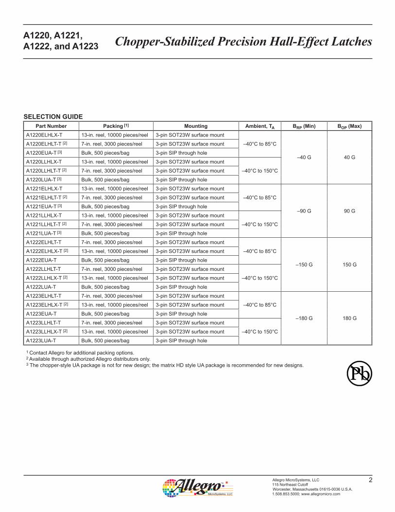
SELECTION GUIDEPart Number Packing [1] Mounting Ambient, TA BRP (Min) BOP (Max)
A1220ELHLX-T 13-in. reel, 10000 pieces/reel 3-pin SOT23W surface mount
–40°C to 85°C
–40 G 40 G
A1220ELHLT-T [2] 7-in. reel, 3000 pieces/reel 3-pin SOT23W surface mount
A1220EUA-T [3] Bulk, 500 pieces/bag 3-pin SIP through hole
A1220LLHLX-T 13-in. reel, 10000 pieces/reel 3-pin SOT23W surface mount
–40°C to 150°CA1220LLHLT-T [2] 7-in. reel, 3000 pieces/reel 3-pin SOT23W surface mount
A1220LUA-T [3] Bulk, 500 pieces/bag 3-pin SIP through hole
A1221ELHLX-T 13-in. reel, 10000 pieces/reel 3-pin SOT23W surface mount
–40°C to 85°C
–90 G 90 G
A1221ELHLT-T [2] 7-in. reel, 3000 pieces/reel 3-pin SOT23W surface mount
A1221EUA-T [3] Bulk, 500 pieces/bag 3-pin SIP through hole
A1221LLHLX-T 13-in. reel, 10000 pieces/reel 3-pin SOT23W surface mount
–40°C to 150°CA1221LLHLT-T [2] 7-in. reel, 3000 pieces/reel 3-pin SOT23W surface mount
A1221LUA-T [3] Bulk, 500 pieces/bag 3-pin SIP through hole
A1222ELHLT-T 7-in. reel, 3000 pieces/reel 3-pin SOT23W surface mount
–40°C to 85°C
–150 G 150 G
A1222ELHLX-T [2] 13-in. reel, 10000 pieces/reel 3-pin SOT23W surface mount
A1222EUA-T Bulk, 500 pieces/bag 3-pin SIP through hole
A1222LLHLT-T 7-in. reel, 3000 pieces/reel 3-pin SOT23W surface mount
–40°C to 150°CA1222LLHLX-T [2] 13-in. reel, 10000 pieces/reel 3-pin SOT23W surface mount
A1222LUA-T Bulk, 500 pieces/bag 3-pin SIP through hole
A1223ELHLT-T 7-in. reel, 3000 pieces/reel 3-pin SOT23W surface mount
–40°C to 85°C
–180 G 180 G
A1223ELHLX-T [2] 13-in. reel, 10000 pieces/reel 3-pin SOT23W surface mount
A1223EUA-T Bulk, 500 pieces/bag 3-pin SIP through hole
A1223LLHLT-T 7-in. reel, 3000 pieces/reel 3-pin SOT23W surface mount
–40°C to 150°CA1223LLHLX-T [2] 13-in. reel, 10000 pieces/reel 3-pin SOT23W surface mount
A1223LUA-T Bulk, 500 pieces/bag 3-pin SIP through hole
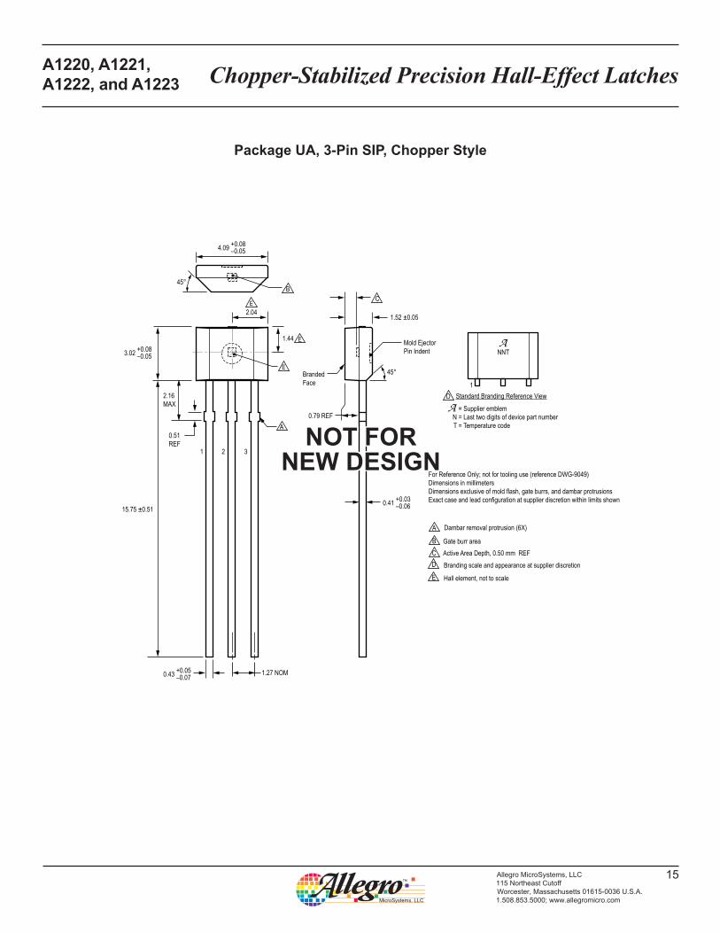
1 Contact Allegro for additional packing options. 2 Available through authorized Allegro distributors only.3 The chopper-style UA package is not for new design; the matrix HD style UA package is recommended for new designs.
Chopper-Stabilized Precision Hall-Effect LatchesA1220, A1221, A1222, and A1223
3Allegro MicroSystems, LLC115 Northeast CutoffWorcester, Massachusetts 01615-0036 U.S.A.1.508.853.5000; www.allegromicro.com
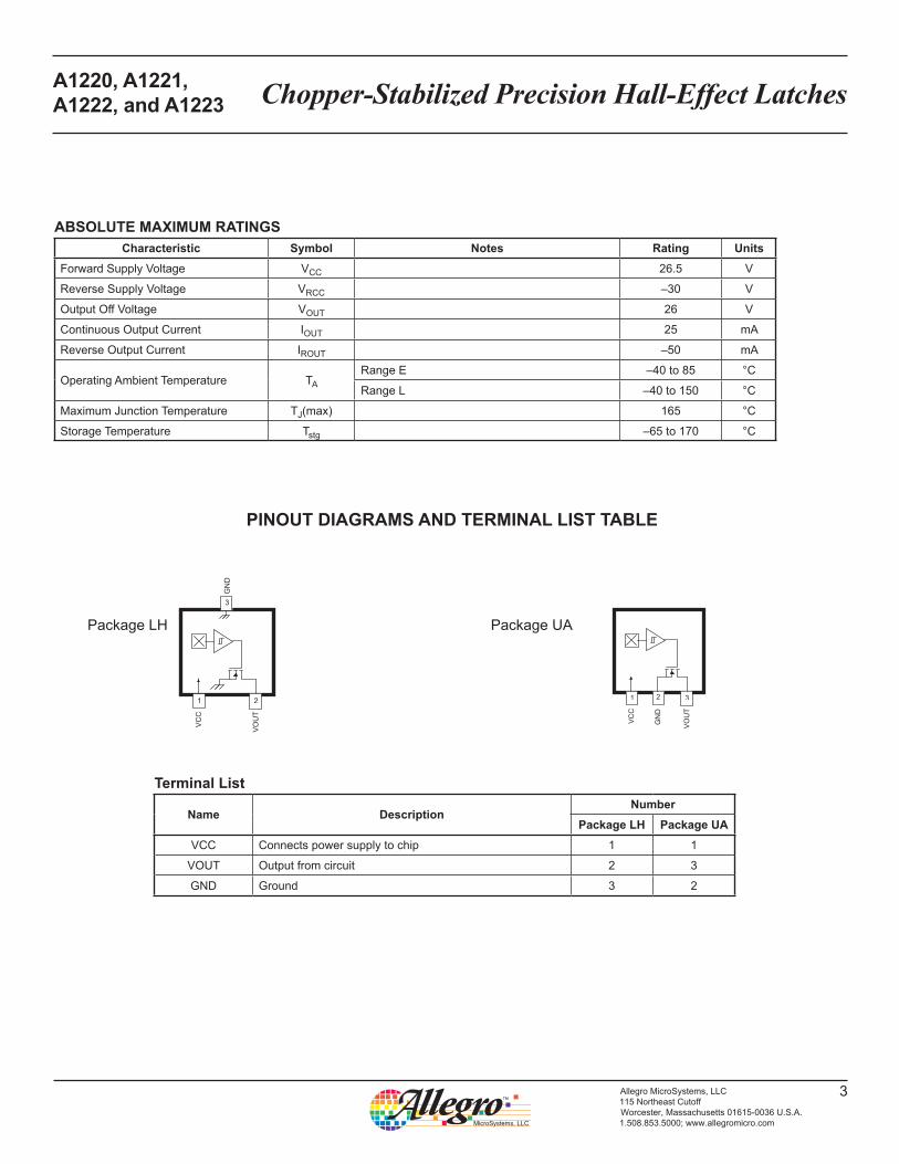
ABSOLUTE MAXIMUM RATINGSCharacteristic Symbol Notes Rating Units
Forward Supply Voltage VCC 26.5 V
Reverse Supply Voltage VRCC –30 V
Output Off Voltage VOUT 26 V
Continuous Output Current IOUT 25 mA
Reverse Output Current IROUT –50 mA
Operating Ambient Temperature TARange E –40 to 85 °C
Range L –40 to 150 °C
Maximum Junction Temperature TJ(max) 165 °C
Storage Temperature Tstg –65 to 170 °C
PINOUT DIAGRAMS AND TERMINAL LIST TABLE
Terminal List
Name DescriptionNumber
Package LH Package UAVCC Connects power supply to chip 1 1
VOUT Output from circuit 2 3
GND Ground 3 2
1 32
GND
VOUT
VCC
Package UAPackage LH
1 2
3
GND
VOUT
VCC
Chopper-Stabilized Precision Hall-Effect LatchesA1220, A1221, A1222, and A1223
4Allegro MicroSystems, LLC115 Northeast CutoffWorcester, Massachusetts 01615-0036 U.S.A.1.508.853.5000; www.allegromicro.com
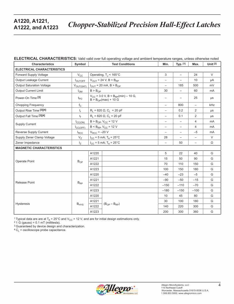
ELECTRICAL CHARACTERISTICS: Valid valid over full operating voltage and ambient temperature ranges, unless otherwise notedCharacteristics Symbol Test Conditions Min. Typ. [1] Max. Unit [2]
ELECTRICAL CHARACTERISTICSForward Supply Voltage VCC Operating, TJ < 165°C 3 – 24 V
Output Leakage Current IOUTOFF VOUT = 24 V, B < BRP – – 10 µA
Output Saturation Voltage VOUT(SAT) IOUT = 20 mA, B > BOP – 185 500 mV
Output Current Limit IOM B > BOP 30 – 60 mA
Power-On Time [3] tPOVCC > 3.0 V, B < BRP(min) – 10 G, B > BOP(max) + 10 G – – 25 µs
Chopping Frequency fC – 800 – kHz
Output Rise Time [3][4] tr RL = 820 Ω, CL = 20 pF – 0.2 2 µs
Output Fall Time [3][4] tf RL = 820 Ω, CL = 20 pF – 0.1 2 µs
Supply CurrentICC(ON) B > BOP, VCC = 12 V – – 4 mA
ICC(OFF) B < BRP, VCC = 12 V – – 4 mA
Reverse Supply Current IRCC VRCC = –20 V – – –5 mA
Supply Zener Clamp Voltage VZ ICC = 5 mA; TA = 25°C 28 – – V
Zener Impedance IZ ICC = 5 mA; TA = 25°C – 50 – Ω
MAGNETIC CHARACTERISTICS
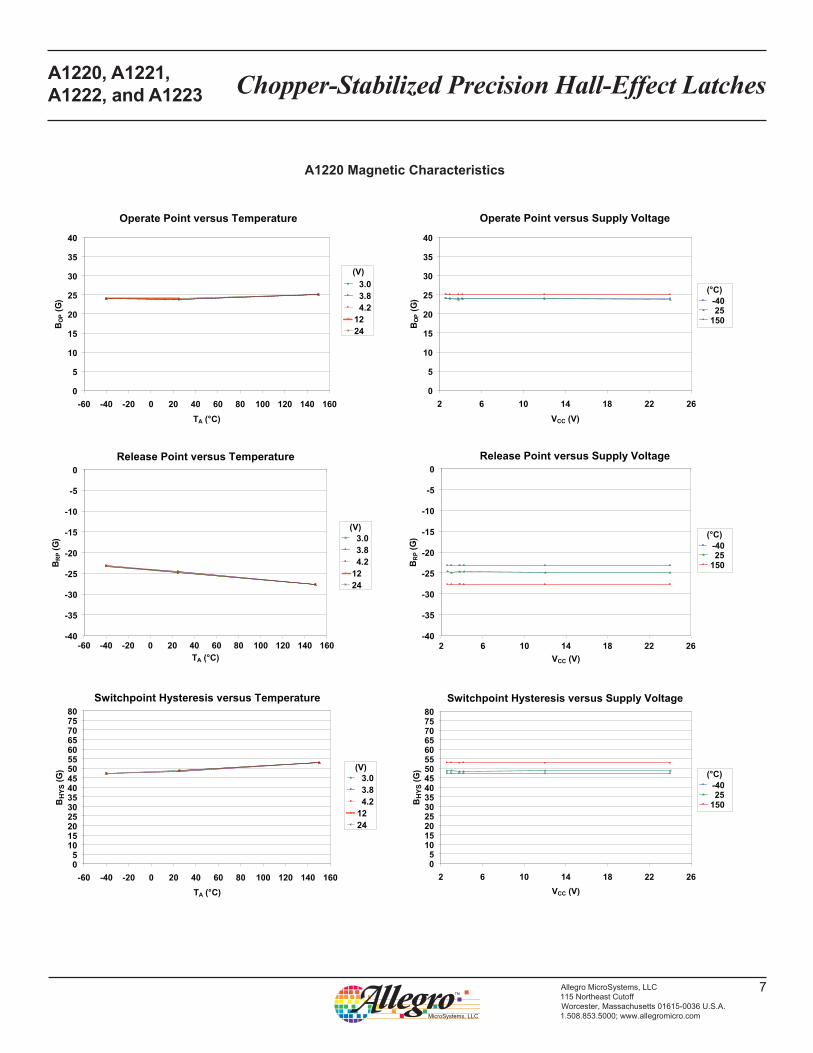
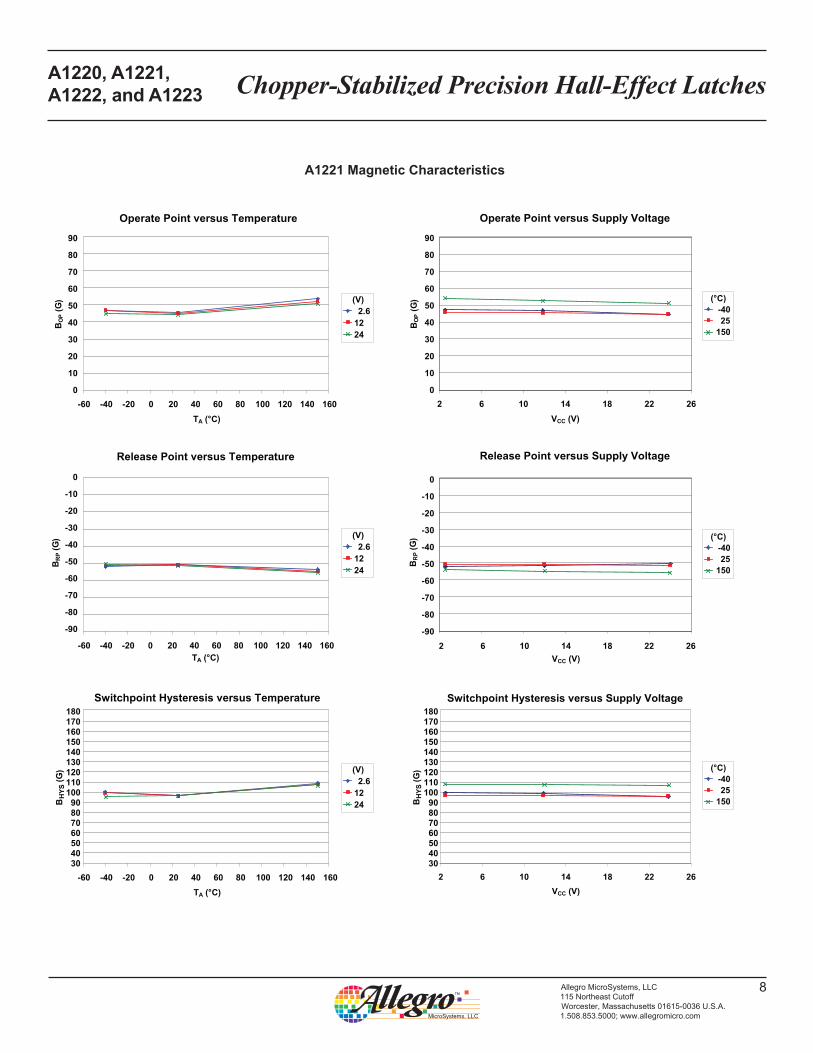
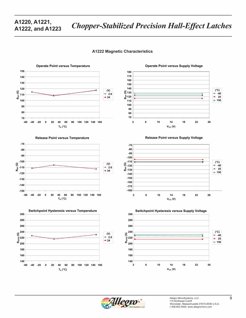
Operate Point BOP
A1220 5 22 40 G
A1221 15 50 90 G
A1222 70 110 150 G
A1223 100 150 180 G
Release Point BRP
A1220 –40 –23 –5 G
A1221 –90 –50 –15 G
A1222 –150 –110 –70 G
A1223 –180 –150 –100 G
Hysteresis BHYS
A1220
(BOP – BRP)
10 45 80 G
A1221 30 100 180 G
A1222 140 220 300 G
A1223 200 300 360 G
1 Typical data are are at TA = 25°C and VCC = 12 V, and are for initial design estimations only.2 1 G (gauss) = 0.1 mT (millitesla).3 Guaranteed by device design and characterization.4 CL = oscilloscope probe capacitance.
Chopper-Stabilized Precision Hall-Effect LatchesA1220, A1221, A1222, and A1223
5Allegro MicroSystems, LLC115 Northeast CutoffWorcester, Massachusetts 01615-0036 U.S.A.1.508.853.5000; www.allegromicro.com
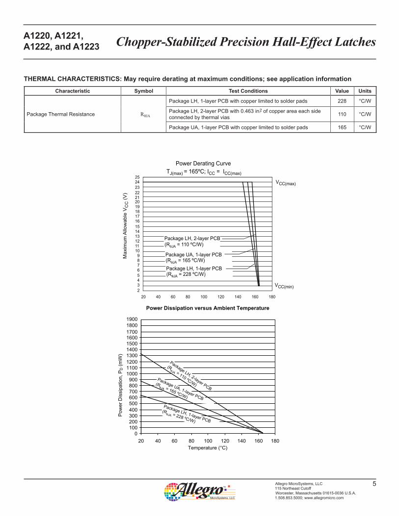
THERMAL CHARACTERISTICS: May require derating at maximum conditions; see application information
Characteristic Symbol Test Conditions Value Units
Package Thermal Resistance RθJA
Package LH, 1-layer PCB with copper limited to solder pads 228 °C/W
Package LH, 2-layer PCB with 0.463 in.2 of copper area each side connected by thermal vias 110 °C/W
Package UA, 1-layer PCB with copper limited to solder pads 165 °C/W
6789
2345
10111213141516171819202122232425
20 40 60 80 100 120 140 160 180
Temperature (ºC)
Max
imum
Allo
wab
le V
CC
(V)
TJ(max) = 165ºC; ICC = ICC(max)
Power Derating Curve
(RθJA = 228 ºC/W)Package LH, 1-layer PCB
(RθJA = 110 ºC/W)Package LH, 2-layer PCB
(RθJA = 165 ºC/W)Package UA, 1-layer PCB
VCC(min)
VCC(max)
0100200300400500600700800900
1000110012001300140015001600170018001900
20 40 60 80 100 120 140 160 180Temperature (°C)
Pow
er D
issi
patio
n, P
D (m
W)
Power Dissipation versus Ambient Temperature
(RθJA = 165 ºC/W)
Package UA, 1-layer PCB
(RθJA = 228 ºC/W)
Package LH, 1-layer PCB
(RθJA = 110 ºC/W)
Package LH, 2-layer PCB
Chopper-Stabilized Precision Hall-Effect LatchesA1220, A1221, A1222, and A1223
6Allegro MicroSystems, LLC115 Northeast CutoffWorcester, Massachusetts 01615-0036 U.S.A.1.508.853.5000; www.allegromicro.com
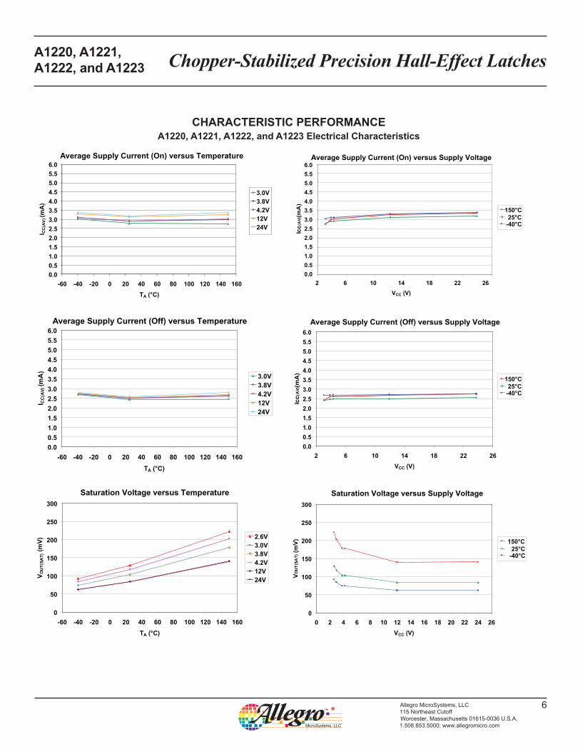
Average Supply Current (On) versus Temperature
0.00.51.01.52.02.53.03.54.04.55.05.56.0
-60 -40 -20 0 20 40 60 80 100 120 140 160TA (°C)
I CC
(AV
) (m
A)
Average Supply Current (On) versus Supply Voltage
0.00.51.01.52.02.53.03.54.04.55.05.56.0
2 6 10 14 18 22 26VCC (V)
Icc(
AV)
(mA
)
Average Supply Current (Off) versus Temperature
0.00.51.01.52.02.53.03.54.04.55.05.56.0
-60 -40 -20 0 20 40 60 80 100 120 140 160TA (°C)
I CC
(AV)
(mA
)
Average Supply Current (Off) versus Supply Voltage
0.00.51.01.52.02.53.03.54.04.55.05.56.0
2 6 10 14 18 22 26VCC (V)
Icc(
AV)
(mA
)
Saturation Voltage versus Temperature
0
50
100
150
200
250
300
-60 -40 -20 0 20 40 60 80 100 120 140 160TA (°C)
V OU
T(SA
T) (m
V)
2.6V3.0V3.8V4.2V12V24V
Saturation Voltage versus Supply Voltage
0
50
100
150
200
250
300
0 2 4 6 8 10 12 14 16 18 20 22 24 26VCC (V)
VOU
T(SA
T) (m
V)
3.0V3.8V4.2V12V24V
150°C
-40°C25°C
150°C
-40°C25°C
150°C
-40°C25°C
3.0V3.8V4.2V12V24V
CHARACTERISTIC PERFORMANCEA1220, A1221, A1222, and A1223 Electrical Characteristics
Chopper-Stabilized Precision Hall-Effect LatchesA1220, A1221, A1222, and A1223
7Allegro MicroSystems, LLC115 Northeast CutoffWorcester, Massachusetts 01615-0036 U.S.A.1.508.853.5000; www.allegromicro.com
150
-4025
(°C)
150
-4025
(°C)
150
-4025
(°C)
Operate Point versus Temperature
0
5
10
15
20
25
30
35
40
-60 -40 -20 0 20 40 60 80 100 120 140 160TA (°C)
BO
P (G
)
3.03.84.2
1224
Operate Point versus Supply Voltage
0
5
10
15
20
25
30
35
40
2 6 10 14 18 22 26VCC (V)
BO
P (G
)
Release Point versus Temperature
-40
-35
-30
-25
-20
-15
-10
-5
0
-60 -40 -20 0 20 40 60 80 100 120 140 160TA (°C)
BR
P (G
)
3.03.84.2
1224
Release Point versus Supply Voltage
-40
-35
-30
-25
-20
-15
-10
-5
0
2 6 10 14 18 22 26VCC (V)
BR
P (G
)
Switchpoint Hysteresis versus Temperature
05
101520253035404550556065707580
-60 -40 -20 0 20 40 60 80 100 120 140 160TA (°C)
BH
YS (G
)
3.03.84.2
1224
Switchpoint Hysteresis versus Supply Voltage
05
101520253035404550556065707580
2 6 10 14 18 22 26VCC (V)
BH
YS (G
)
(V)
(V)
(V)
A1220 Magnetic Characteristics
Chopper-Stabilized Precision Hall-Effect LatchesA1220, A1221, A1222, and A1223
8Allegro MicroSystems, LLC115 Northeast CutoffWorcester, Massachusetts 01615-0036 U.S.A.1.508.853.5000; www.allegromicro.com
Operate Point versus Temperature
90
80
70
60
50
40
30
20
10
0
0
-10
-20
-30
-40
-50
-60
-70
-80
-90
-60 -40 -20 0 20 40 60 80 100 120 140 160TA (°C)
BO
P (G
)
Operate Point versus Supply Voltage
90
80
70
60
50
40
30
20
10
0
0
-10
-20
-30
-40
-50
-60
-70
-80
-90
2 6 10 14 18 22 26VCC (V)
BO
P (G
)
Release Point versus Temperature
-60 -40 -20 0 20 40 60 80 100 120 140 160TA (°C)
BR
P (G
)
Release Point versus Supply Voltage
2 6 10 14 18 22 26VCC (V)
BR
P (G
)
Switchpoint Hysteresis versus Temperature18017016015014013012011010090807060504030
-60 -40 -20 0 20 40 60 80 100 120 140 160TA (°C)
BH
YS (G
)
Switchpoint Hysteresis versus Supply Voltage
2 6 10 14 18 22 26VCC (V)
BH
YS (G
)
18017016015014013012011010090807060504030
2.6 1224
(V)
2.6 1224
(V)
2.6 1224
(V)
150
-4025
(°C)
150
-4025
(°C)
150
-4025
(°C)
A1221 Magnetic Characteristics
Chopper-Stabilized Precision Hall-Effect LatchesA1220, A1221, A1222, and A1223
9Allegro MicroSystems, LLC115 Northeast CutoffWorcester, Massachusetts 01615-0036 U.S.A.1.508.853.5000; www.allegromicro.com
Operate Point versus Temperature150
140
130
120
110
100
90
80
70
-70
-80
-90
-100
-110
-120
-130
-140
-150
-60 -40 -20 0 20 40 60 80 100 120 140 160TA (°C)
BO
P (G
)
Operate Point versus Supply Voltage
180170160150140130120110100908070
-70-80-90
-100-110-120-130-140-150-160-170-180
2 6 10 14 18 22 26VCC (V)
BO
P (G
)
Release Point versus Temperature
-60 -40 -20 0 20 40 60 80 100 120 140 160TA (°C)
BR
P (G
)
Release Point versus Supply Voltage
2 6 10 14 18 22 26VCC (V)
BR
P (G
)
Switchpoint Hysteresis versus Temperature300
280
260
240
220
200
180
160
140-60 -40 -20 0 20 40 60 80 100 120 140 160
TA (°C)
BH
YS (G
)
Switchpoint Hysteresis versus Supply Voltage
2 6 10 14 18 22 26VCC (V)
BH
YS (G
)
300
280
260
240
220
200
180
160
140
2.6 24
(V)
2.6 24
(V)
2.6 24
(V)
150
-4025
(°C)
150
-4025
(°C)
150
-4025
(°C)
A1222 Magnetic Characteristics
Chopper-Stabilized Precision Hall-Effect LatchesA1220, A1221, A1222, and A1223
10Allegro MicroSystems, LLC115 Northeast CutoffWorcester, Massachusetts 01615-0036 U.S.A.1.508.853.5000; www.allegromicro.com
CBYPA122x
VOUT
GND
0.1 µF
VCC
Output
RL
VS
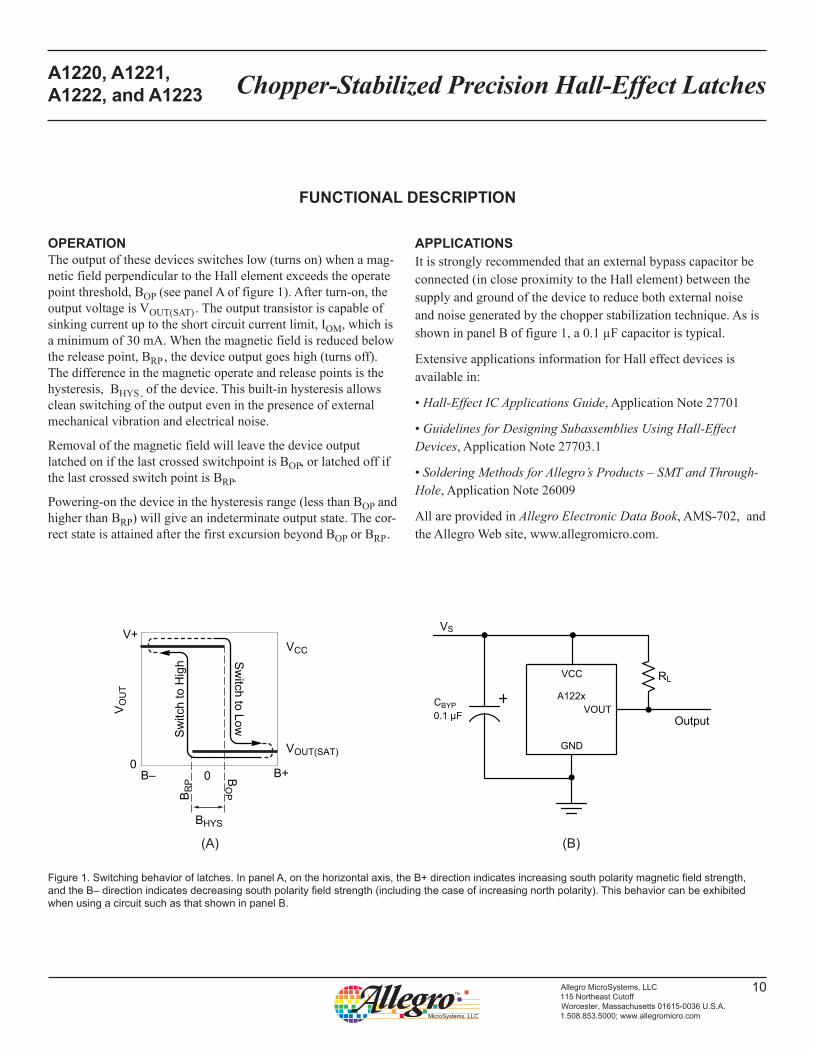
OPERATIONThe output of these devices switches low (turns on) when a mag-netic field perpendicular to the Hall element exceeds the operate point threshold, BOP (see panel A of figure 1). After turn-on, the output voltage is VOUT(SAT) . The output transistor is capable of sinking current up to the short circuit current limit, IOM, which is a minimum of 30 mA. When the magnetic field is reduced below the release point, BRP , the device output goes high (turns off). The difference in the magnetic operate and release points is the hysteresis, BHYS , of the device. This built-in hysteresis allows clean switching of the output even in the presence of external mechanical vibration and electrical noise.
Removalofthemagneticfieldwillleavethedeviceoutputlatched on if the last crossed switchpoint is BOP, or latched off if the last crossed switch point is BRP.
Powering-on the device in the hysteresis range (less than BOP and higher than BRP) will give an indeterminate output state. The cor-rect state is attained after the first excursion beyond BOP or BRP.
APPLICATIONSIt is strongly recommended that an external bypass capacitor be connected (in close proximity to the Hall element) between the supply and ground of the device to reduce both external noise andnoisegeneratedbythechopperstabilizationtechnique.Asisshown in panel B of figure 1, a 0.1 µF capacitor is typical.
Extensive applications information for Hall effect devices is available in:
• Hall-Effect IC Applications Guide, Application Note 27701
• Guidelines for Designing Subassemblies Using Hall-Effect Devices, Application Note 27703.1
• Soldering Methods for Allegro’s Products – SMT and Through-Hole, Application Note 26009
All are provided in Allegro Electronic Data Book, AMS-702, and the Allegro Web site, www.allegromicro.com.
Figure 1. Switching behavior of latches. In panel A, on the horizontal axis, the B+ direction indicates increasing south polarity magnetic field strength, and the B– direction indicates decreasing south polarity field strength (including the case of increasing north polarity). This behavior can be exhibited when using a circuit such as that shown in panel B.
(A) (B)
FUNCTIONAL DESCRIPTION
BO
PBR
P
BHYS
VCC
VO
UT
VOUT(SAT)
Sw
itch to Low
Sw
itch
to H
igh
B+B–
V+
00
Chopper-Stabilized Precision Hall-Effect LatchesA1220, A1221, A1222, and A1223
11Allegro MicroSystems, LLC115 Northeast CutoffWorcester, Massachusetts 01615-0036 U.S.A.1.508.853.5000; www.allegromicro.com
Amp
Regulator
Clock/Logic
Hall Element
Sam
ple
and
Hol
d
Low-PassFilter
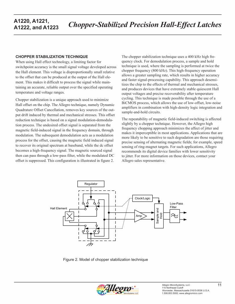
CHOPPER STABILIZATION TECHNIQUEWhen using Hall effect technology, a limiting factor for switchpoint accuracy is the small signal voltage developed across the Hall element. This voltage is disproportionally small relative to the offset that can be produced at the output of the Hall ele-ment. This makes it difficult to process the signal while main-taining an accurate, reliable output over the specified operating temperature and voltage ranges.
ChopperstabilizationisauniqueapproachusedtominimizeHalloffsetonthechip.TheAllegrotechnique,namelyDynamicQuadratureOffsetCancellation,removeskeysourcesoftheout-put drift induced by thermal and mechanical stresses. This offset reductiontechniqueisbasedonasignalmodulation-demodula-tion process. The undesired offset signal is separated from the magneticfield-inducedsignalinthefrequencydomain,throughmodulation.Thesubsequentdemodulationactsasamodulationprocess for the offset, causing the magnetic field induced signal to recover its original spectrum at baseband, while the dc offset becomesahigh-frequencysignal.Themagneticsourcedsignalthencanpassthroughalow-passfilter,whilethemodulatedDCoffset is suppressed. This configuration is illustrated in figure 2.
Thechopperstabilizationtechniqueusesa400kHzhighfre-quencyclock.Fordemodulationprocess,asampleandholdtechniqueisused,wherethesamplingisperformedattwicethechopperfrequency(800kHz).Thishigh-frequencyoperationallows a greater sampling rate, which results in higher accuracy and faster signal-processing capability. This approach desensi-tizes the chip to the effects of thermal and mechanical stresses, andproducesdevicesthathaveextremelystablequiescentHalloutput voltages and precise recoverability after temperature cycling.ThistechniqueismadepossiblethroughtheuseofaBiCMOS process, which allows the use of low-offset, low-noise amplifiers in combination with high-density logic integration and sample-and-hold circuits.
The repeatability of magnetic field-induced switching is affected slightlybyachoppertechnique.However,theAllegrohighfrequencychoppingapproachminimizestheaffectofjitterandmakes it imperceptible in most applications. Applications that are morelikelytobesensitivetosuchdegradationarethoserequiringprecise sensing of alternating magnetic fields; for example, speed sensing of ring-magnet targets. For such applications, Allegro recommends its digital device families with lower sensitivity tojitter.Formoreinformationonthosedevices,contactyourAllegro sales representative.
Figure 2. Model of chopper stabilization technique
Chopper-Stabilized Precision Hall-Effect LatchesA1220, A1221, A1222, and A1223
12Allegro MicroSystems, LLC115 Northeast CutoffWorcester, Massachusetts 01615-0036 U.S.A.1.508.853.5000; www.allegromicro.com
POWER DERATINGThedevicemustbeoperatedbelowthemaximumjunctiontemperature of the device, TJ(max). Under certain combinations of peakconditions,reliableoperationmayrequirederatingsuppliedpower or improving the heat dissipation properties of the appli-cation. This section presents a procedure for correlating factors affecting operating TJ. (Thermal data is also available on the Allegro MicroSystems website.)
ThePackageThermalResistance,RθJA, is a figure of merit sum-marizing the ability of the application and the device to dissipate heatfromthejunction(die),throughallpathstotheambientair.Its primary component is the Effective Thermal Conductivity, K, oftheprintedcircuitboard,includingadjacentdevicesandtraces.Radiationfromthediethroughthedevicecase,RθJC, is relatively smallcomponentofRθJA. Ambient air temperature, TA, and air motion are significant external factors, damped by overmolding.
Theeffectofvaryingpowerlevels(PowerDissipation,PD), can be estimated. The following formulas represent the fundamental relationships used to estimate TJ, at PD.
PD = VIN × IIN (1)
ΔT = PD × RθJA (2)
TJ = TA + ΔT (3)
For example, given common conditions such as: TA= 25°C, VCC = 12 V, ICC = 1.6 mA, and RθJA = 165 °C/W, then:
PD = VCC × ICC = 12 V × 1.6 mA = 19 mW
ΔT = PD × RθJA = 19 mW × 165 °C/W = 3°C
TJ = TA + ΔT = 25°C + 3°C = 28°CA worst-case estimate, PD(max), represents the maximum allow-able power level (VCC(max), ICC(max)), without exceeding TJ(max), ataselectedRθJA and TA.
Example:ReliabilityforVCC at TA = 150°C, package LH, using a minimum-K PCB.
Observe the worst-case ratings for the device, specifically: RθJA= 228°C/W,TJ(max) = 165°C, VCC(max) = 24 V, and ICC(max) = 4 mA.
Calculate the maximum allowable power level, PD(max). First, invertequation3:
ΔTmax = TJ(max) – TA = 165 °C – 150 °C = 15 °C
This provides the allowable increase to TJ resulting from internal powerdissipation.Then,invertequation2:
PD(max) = ΔTmax ÷ RθJA = 15°C ÷ 228 °C/W = 66 mWFinally,invertequation1withrespecttovoltage:
VCC(est) = PD(max) ÷ ICC(max) = 66 mW ÷ 4 mA = 16.4 V
The result indicates that, at TA, the application and device can dissipateadequateamountsofheatatvoltages≤VCC(est).
Compare VCC(est) to VCC(max). If VCC(est)≤VCC(max), then reli-able operation between VCC(est) and VCC(max)requiresenhancedRθJA. If VCC(est)≥VCC(max), then operation between VCC(est) and VCC(max) is reliable under these conditions.
Chopper-Stabilized Precision Hall-Effect LatchesA1220, A1221, A1222, and A1223
13Allegro MicroSystems, LLC115 Northeast CutoffWorcester, Massachusetts 01615-0036 U.S.A.1.508.853.5000; www.allegromicro.com
0.55 REF
Gauge PlaneSeating Plane
0.25 BSC
0.95 BSC
0.95
1.00
0.70 2.40
21
A Active Area Depth, 0.28 mm REFB
C
B
Reference land pattern layout All pads a minimum of 0.20 mm from all adjacent pads; adjust as necessary to meet application process requirements and PCB layout tolerancesBranding scale and appearance at supplier discretion
A
PCB Layout Reference View
Branded Face
C Standard Branding Reference View
N = Last two digits of device part number T = Temperature code (letter)
1
NNT
N = Last three digits of device part number1
NNN
2.90 +0.10–0.20
4°±4°
8X 10° REF
0.180+0.020–0.053
0.05 +0.10–0.05
0.25 MIN
1.91 +0.19–0.06
2.98 +0.12–0.08
1.00 ±0.13
0.40 ±0.10
For Reference Only; not for tooling use (reference dwg. 802840)Dimensions in millimetersDimensions exclusive of mold flash, gate burrs, and dambar protrusions Exact case and lead configuration at supplier discretion within limits shown
D Hall element, not to scale
D
D
D1.49
0.96
3
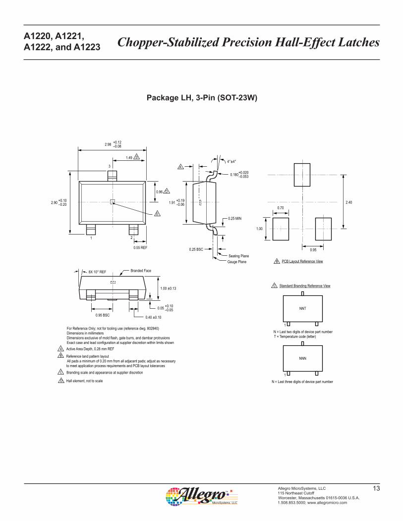
Package LH, 3-Pin (SOT-23W)
Chopper-Stabilized Precision Hall-Effect LatchesA1220, A1221, A1222, and A1223
14Allegro MicroSystems, LLC115 Northeast CutoffWorcester, Massachusetts 01615-0036 U.S.A.1.508.853.5000; www.allegromicro.com
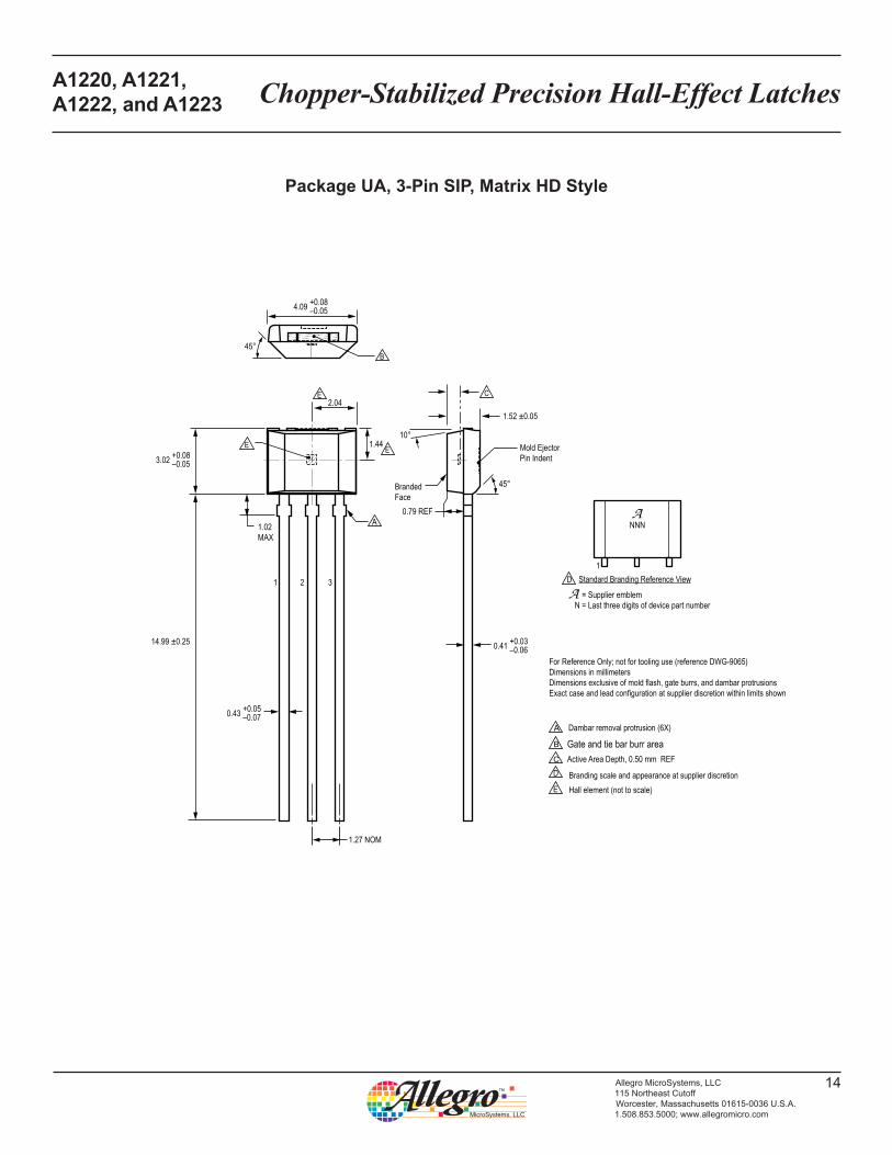
Package UA, 3-Pin SIP, Matrix HD Style
2 31
1.27 NOM
1.02 MAX
45°
45°
C
1.52 ±0.05
B
Gate and tie bar burr areaA
B
C
Dambar removal protrusion (6X)
A
D
E
E
E
1.44
2.04
E
Active Area Depth, 0.50 mm REF
Branding scale and appearance at supplier discretionHall element (not to scale)
For Reference Only; not for tooling use (reference DWG-9065)Dimensions in millimetersDimensions exclusive of mold flash, gate burrs, and dambar protrusions Exact case and lead configuration at supplier discretion within limits shown
Mold EjectorPin Indent
D Standard Branding Reference View
= Supplier emblem N = Last three digits of device part number
NNN
1
0.41 +0.03–0.06
0.43 +0.05–0.07
14.99 ±0.25
4.09 +0.08–0.05
3.02 +0.08–0.05
0.79 REF
10°
Branded Face
Chopper-Stabilized Precision Hall-Effect LatchesA1220, A1221, A1222, and A1223
15Allegro MicroSystems, LLC115 Northeast CutoffWorcester, Massachusetts 01615-0036 U.S.A.1.508.853.5000; www.allegromicro.com
Package UA, 3-Pin SIP, Chopper Style
2 31
0.79 REF
1.27 NOM
2.16 MAX
0.51REF
45°
C
45°
B
E
E
E2.04
1.44
Gate burr area
A
BC
Dambar removal protrusion (6X)
A
D
E
D
Branding scale and appearance at supplier discretion
Hall element, not to scale
Active Area Depth, 0.50 mm REF
For Reference Only; not for tooling use (reference DWG-9049)Dimensions in millimetersDimensions exclusive of mold flash, gate burrs, and dambar protrusions Exact case and lead configuration at supplier discretion within limits shown
Standard Branding Reference View
= Supplier emblem N = Last two digits of device part number T = Temperature code
NNT
1
Mold EjectorPin Indent
Branded Face
4.09 +0.08–0.05
0.41 +0.03–0.06
3.02 +0.08–0.05
0.43 +0.05–0.07
15.75 ±0.51
1.52 ±0.05
NOT FOR NEW DESIGN
Chopper-Stabilized Precision Hall-Effect LatchesA1220, A1221, A1222, and A1223
16Allegro MicroSystems, LLC115 Northeast CutoffWorcester, Massachusetts 01615-0036 U.S.A.1.508.853.5000; www.allegromicro.com
Copyright ©2016, Allegro MicroSystems, LLCAllegro MicroSystems, LLC reserves the right to make, from time to time, such departures from the detail specifications as may be required to
permit improvements in the performance, reliability, or manufacturability of its products. Before placing an order, the user is cautioned to verify that the information being relied upon is current.
Allegro’s products are not to be used in any devices or systems, including but not limited to life support devices or systems, in which a failure of Allegro’s product can reasonably be expected to cause bodily harm.
The information included herein is believed to be accurate and reliable. However, Allegro MicroSystems, LLC assumes no responsibility for its use; nor for any infringement of patents or other rights of third parties which may result from its use.
For the latest version of this document, visit our website: www.allegromicro.com
Revision HistoryNumber Date Description
15 September 16, 2013 Update UA package drawing16 September 21, 2015 Added AEC-Q100 qualification under Features and Benefits17 January 12, 2016 Updated Reverse Supply Current test conditions in Electrical Characteristics table18 October 20, 2016 Chopper-style UA package designated as not for new design