Embed Size (px)
Citation preview

HAL Id: hal-00526208https://hal.archives-ouvertes.fr/hal-00526208
Submitted on 14 Oct 2010
HAL is a multi-disciplinary open accessarchive for the deposit and dissemination of sci-entific research documents, whether they are pub-lished or not. The documents may come fromteaching and research institutions in France orabroad, or from public or private research centers.
L’archive ouverte pluridisciplinaire HAL, estdestinée au dépôt et à la diffusion de documentsscientifiques de niveau recherche, publiés ou non,émanant des établissements d’enseignement et derecherche français ou étrangers, des laboratoirespublics ou privés.
Compact Modeling of Symmetrical Double-GateMOSFETs Including Carrier Confinement and
Short-Channel EffectsDaniela Munteanu, Jean-Luc Autran, Xavier Loussier, Samuel Harrison,
Robin Cerutti
To cite this version:Daniela Munteanu, Jean-Luc Autran, Xavier Loussier, Samuel Harrison, Robin Cerutti. Com-pact Modeling of Symmetrical Double-Gate MOSFETs Including Carrier Confinement andShort-Channel Effects. Molecular Simulation, Taylor & Francis, 2007, 33 (07), pp.605-611.�10.1080/08927020600930524�. �hal-00526208�

For Peer Review O
nly
Compact Modeling of Symmetrical Double-Gate MOSFETs Including Carrier Confinement and Short-Channel Effects
Journal: Molecular Simulation/Journal of Experimental Nanoscience
Manuscript ID: GMOS-2006-0102.R1
Journal: Molecular Simulation
Date Submitted by the Author:
24-Jul-2006
Complete List of Authors: Munteanu, Daniela; L2MP-CNRS, Bat. IRPHE Autran, Jean Luc; L2MP-CNRS, Bat. IRPHE; IUF Loussier, Xavier; L2MP-CNRS, Bat. IRPHE Harrison, Samuel; L2MP-CNRS, Bat. IRPHE; STMicroelectronics Cerutti, Robin; STMicroelectronics
Keywords: compact modeling, Double-Gate MOSFET, quantum effects, short-channel effects
http://mc.manuscriptcentral.com/tandf/jenmol

For Peer Review O
nly
Compact Modeling of Symmetrical Double-Gate MOSFETs
Including Carrier Confinement and Short-Channel Effects
D. Munteanu *1, J.L. Autran1,2, X. Loussier1, S. Harrison1,3, R. Cerutti3
1 L2MP, 49 rue Joliot-Curie, BP 146, 13384 Marseille Cedex 13, France
2 also with Institut Universitaire de France (IUF), Paris, France
3 STMicroelectronics, 850 rue J. Monnet, 38926 Crolles France
*Corresponding author:
Dr. Daniela MUNTEANU
L2MP, UMR CNRS 6137
Bât. IRPHE - BP 146
49 rue Joliot-Curie,
F-13384 Marseille Cedex 13, France
Phone: +33 4 96 13 98 19
Fax: +33 4 96 13 97 09
E-mail: [email protected]
Page 1 of 25
http://mc.manuscriptcentral.com/tandf/jenmol
123456789101112131415161718192021222324252627282930313233343536373839404142434445464748495051525354555657585960

For Peer Review O
nly
ABSTRACT
A compact model for the drain current and node charges in symmetrical Double-Gate
MOSFET, including short-channel and carrier confinement effects is developed. The
model is particularly well-adapted to ultra-scaled devices, with short channel lengths
and ultra-thin silicon films. An extensive comparison step with 2D quantum numerical
simulation fully validates the model. The model is also shown to reproduce with an
excellent accuracy experimental drain current measured in Double-Gate devices
fabricated with SON process. Finally, the DG model has been successfully implemented
in Eldo IC analog simulator, demonstrating the application of the model to circuit
simulation.
Keywords: compact modeling, Double-Gate MOSFET, quantum effects, short-channel
effects
Page 2 of 25
http://mc.manuscriptcentral.com/tandf/jenmol
123456789101112131415161718192021222324252627282930313233343536373839404142434445464748495051525354555657585960

For Peer Review O
nly
1. Introduction
Double-Gate (DG) structure has been in the last years the object of intensive research
and an impressing number of studies have confirmed its enormous potentiality to push
back the integration limits to which conventional devices are subjected [1-4]. The main
advantage of this architecture is to offer a reinforced electrostatic coupling between the
conduction channel and the gate electrode. In other terms, a double-gate structure can
efficiently sandwich (and thus very well control, electrostatically speaking) the
semiconductor element playing the role of the transistor channel, which can be a Silicon
thin layer or nanowire, a Carbon nanotube, a molecule or an atomic linear chain. The
MOSFET operation of such ultimate DG devices with a single quantum conduction
channel has been theoretically demonstrated in recent works [5-6].
Although the operation of DG transistor is similar to the conventional MOSFET, the
physics of DG MOSFET is more complicated. Moreover, physical phenomena such as
2D electrostatics or carrier quantization have to be considered, since DG structure will
be precisely used to design very integrated devices (with short channel and extremely
thin films). Therefore, new compact models, dedicated the circuit simulation, have to be
developed for DG MOSFET [4]. Several interesting models have been proposed for the
classical (i.e. without quantum effects) drain current in long channels DG [3-4, 7-9] or
for short channel DG operating in the subthreshold regime [10]. Carrier quantization
effects have been considered for the first time in [11]. In this work, we propose a
compact model which combines short-channel with quantum-mechanical effects and
applies to all operation regimes. In addition the model is continuous over all gate and
drain bias range, which makes it very suitable for implementation in circuit simulators.
The development is based on the calculation of the 2D potential distribution in the
device taking into account the quantum-evaluated inversion charge. A full 2-D quantum
mechanical numerical simulation code [12] is used for completely validating the model.
Page 3 of 25
http://mc.manuscriptcentral.com/tandf/jenmol
123456789101112131415161718192021222324252627282930313233343536373839404142434445464748495051525354555657585960
For Peer Review O
nly
The drain current as predicted by the model is compared with experimental data
measured on scaled DG devices fabricated using the SON (Silicon-on-Nothing) process
[13-14]. Finally, the drain current model is supplemented by a node charge model and
further, the entire DG model is successfully implemented in Eldo IC analog simulator.
2. Drain current modeling
The schematic of a symmetric DG structure and its parameters are shown in Figure 1a.
Figure 1b illustrates the band diagrams in an horizontal cross-section together with the
first energy subbands. The drain current modelling starts with the calculation of the 2D
potential distribution in the DG transistor. For this purpose several methods have been
proposed, the most complete being the evanescent-mode analysis, where the potential is
divided into two different parts )y,x(*)y()y,x( L Ψ+Ψ=Ψ [15]. The first term represents
the long channel solution and the second term takes into account short-channel
behaviour. This last term is then approximated by retaining only the lowest-order mode
from a Fourier expansion of modes. The method can be very powerful for taking into
account short-channel effects in the evaluation of the threshold voltage [15], but the
mathematical development is complicated. For simplifying the calculation, in this work
we assume the following dependence for the potential:
)y,x(VE)x()y,x( s ×Ψ=Ψ (1)
where ΨS is the surface potential and VE(x,y) is the vertical distribution envelope
function. The 2D potential distribution is thus obtained by modulating the surface
potential by an envelope function containing the potential dependence in the vertical
direction. VE(x,y) is then given by:
)0y,x(P)y,x(P)y,x(VE=
= (2)
where P(x,y) is calculated as in [16]:
Page 4 of 25
http://mc.manuscriptcentral.com/tandf/jenmol
123456789101112131415161718192021222324252627282930313233343536373839404142434445464748495051525354555657585960

For Peer Review O
nly
⎪⎭
⎪⎬⎫
⎪⎩
⎪⎨⎧
⎥⎥
⎦
⎤
⎢⎢
⎣
⎡−
εβ−ψ=
−ψβ
)2
ty(ekT2
nqcosln2)y,x(P Si2))x(QFL0(
Si
i2
0 (3)
where β=q/kT, QFL(x) is the quasi-Fermi level and ψ0 are calculated as shown in
[16].
For calculating the vertical distribution envelope function VE(x,y), the expression of
QFL(x) is needed. An analytical expression of QFL(x) has been proposed in [17] for
bulk MOSFET, depending on the x position in the channel, on the channel length and
on the drain voltage. However, our detailed investigation by numerical simulation
showed that the quasi-Fermi level in DG MOSFET also depends on the gate voltage and
on the film thickness. Therefore, we adopted here a quasi-empirical expression
(equation 4) inspired from that proposed in [17] and extensively verified by numerical
simulation:
( ) c3DV
Si
1
FBVGVc
D at1Lx1
q/kTm/Vexplnm
qkT2)x(QFL ×
⎥⎥⎥
⎦
⎤
⎢⎢⎢
⎣
⎡+⎟
⎠⎞
⎜⎝⎛⎟⎟⎠
⎞⎜⎜⎝
⎛−⎟⎟
⎠
⎞⎜⎜⎝
⎛−=
−
− (4)
where ( )FBG VVb2m −+= , 1nm2.0a −= , 1V5.7b −= and V1c = .
The last term to be calculated for obtaining the 2D potential distribution is the surface
potential ΨS(x). As presented in [18], for obtaining the expression of ΨS(x) the Gauss’s
law is applied to the particular closed surface shown in Figure 1a:
Si
i
Si
SiAS
SiSi2
dx)x(Q2
dxtqNdx)x(E2
t)dxx(E2
t)x(Eε
−ε
−=−++− (5)
where E(x) is the electric field, ES(x) is the surface electric field at the Si/SiO2 interface
and NA is the channel doping. Qi(x) is the inversion charge density in the x point of the
channel, calculated by the integration of the electron charge over the Si film thickness.
In the right hand side of equation (5), the first term corresponds to the depletion charge
and the second term corresponds to the mobile inversion charge.
Page 5 of 25
http://mc.manuscriptcentral.com/tandf/jenmol
123456789101112131415161718192021222324252627282930313233343536373839404142434445464748495051525354555657585960

For Peer Review O
nly
In has been shown in reference [13] that for very thin films (<15nm), the electric field
E(x) in equation (5) can be approximated as:
dx)x(d)x(E sΨ−≈ (6)
The following equation can also be written for the electric field:
dx)x(dE
dx)dxx(E)x(E=
++− (7)
In equation (10), the surface electric field at the interface Si/SiO2, ES(x), is obtained
from the boundary conditions at the interface:
Fssoxox
SiFBG EtVV φ+Ψ+
εε
=− (8)
where VFB is the flat-band voltage and φF is the Fermi potential. Replacing (6) in
(7) and then in (5) and using (8), we obtain the following differential equation for
the surface potential ΨS:
[ ]iFFBGoxSiASiSi
sSiSi
ox2s
2Q)VV(C2tqN
t1
tC2
dxd
+φ−−−ε
=Ψε
−Ψ (9)
An approximative analytical solution of equation (9) is given by:
21
1211sm
)x(R)xmexp(C)xmexp(C)x( −−+=Ψ (10)
with C1, C2, m1 and R(x) calculated for filling the boundary conditions ΨS(x=0)=φS and
ΨS(x=L)=φS+VD:
)Lmsinh(2m
)Lmexp(1)0(RV)]Lmexp(1[C
1
21
1D1S
2,1
mm
−++−φ
±= (11)
SiSi
iFFBGoxSiAt
)x(Q)VV(C2tqN)x(Rε
+φ−−−= (12)
)t/(C2m SiSiox1 ε= (13)
( )2iSDAS n/NNln)q/kT(=φ (14)
Page 6 of 25
http://mc.manuscriptcentral.com/tandf/jenmol
123456789101112131415161718192021222324252627282930313233343536373839404142434445464748495051525354555657585960

For Peer Review O
nly
The evaluation of R(x) requires to know the value of the inversion charge density Qi(x),
which can be calculated in two different cases: (a) the "classical" case, i. e. without
quantum confinement effects and (b) the quantum case. In the classical case, the
inversion charge is given by the following equation, assuming a Boltzmann distribution
for the carriers in the channel:
( )[ ]dyeniq)x(Q
Sit
0
)x(QFL)y,x(kTq
i ∫=−Ψ
(15)
In the quantum case, the inversion charge Qi(x) is given by:
⎥⎥⎦
⎤
⎢⎢⎣
⎡⎟⎟⎠
⎞⎜⎜⎝
⎛⎟⎟⎠
⎞⎜⎜⎝
⎛+Ψ−+ξβ−+×∑∑
π= )x(QFL)x(
2E
exp1lngmqkT)x(Q Sgi
t,ll,tt,l i
l,tD22i
h (16)
where mt*=0.19×m0, ml
*=0.98×m0, gl=2, gt=4, β=q/kT, *t
lD2 mm = , *
t*l
tD2 mmm = . In
equation (16) ξil,t are the energy levels calculated using a standard method for first-order
perturbation applied to the energy levels of an infinite rectangular well (as shown in
[13]):
iit,l
it,l )r( ξ∆+ξ=ξ (17)
where (ξr)il,t are the energy levels of an infinite rectangular well. (ξr)il,t is given by the
well-known equation:
2Si
*t,l
222i
t,l tqm2i)r( π
=ξh (18)
and
iii H ϕϕ=ξ∆ (19)
where H is the Hamiltonian of the perturbation and φi are the electron wave functions
associated to energy levels ξil,t. In equation (11), R(0) is calculated considering Qi(0)
given by equation (15) or (16) with ΨS(0)=φS.
Page 7 of 25
http://mc.manuscriptcentral.com/tandf/jenmol
123456789101112131415161718192021222324252627282930313233343536373839404142434445464748495051525354555657585960

For Peer Review O
nly
Since ΨS(x) given by equation (10) depends on Qi(x), replacing (10) and (17) in (16)
leads to an implicit equation on Qi(x), which is solved numerically for obtaining Qi(x).
Finally, for calculating the drain current in DG MOSFET we express the current density
(including both the drift and the diffusion components) as:
dx)x(dQFL)y,x(qµnJ −= (20)
which is then integrated in y and z directions:
dx)x(dQFL)x(µWQ)x(I id = (21)
Current continuity requires the drain current be independent of x and therefore,
integrating equation (21) in x direction from x=0 to x=L gives the final expression of ID:
∫=DV
0iD )x(dQFL)x(Q
LWµI (22)
In the classical case and considering the Boltzmann distribution for the carriers,
equation (21) becomes [10]:
( )
∫
∫
−−=
ψ
L
0 Sit
0
kT/)y,x(qi
DD
dxeqn
dykT/qVexp1
qkTµWI (23)
3. Model validation by numerical simulation: short-channel, quantum effects and
volume inversion
The model was validated by an extensive comparison with quantum numerical
simulation using a full 2-D Poisson-Schrödinger code [12]. In a first step, the potential
distribution as given by equation (1) has been extensively validated for various structure
parameters and biases. An example is shown in Figures 2a, where the surface potential
as given by the model for L=50nm and L=10nm is compared with numerical simulation.
In Figure 2b, the potential distribution in a vertical cut-line perpendicular to the Si film
(in the middle of the channel, y direction) is illustrated. A good agreement is obtained
Page 8 of 25
http://mc.manuscriptcentral.com/tandf/jenmol
123456789101112131415161718192021222324252627282930313233343536373839404142434445464748495051525354555657585960

For Peer Review O
nly
between the model and the numerical simulation. The variation of the quasi-Fermi level
(equation 4) was also validated as presented in Figure 3. Equation (3) has been derived
under classical assumptions, but we verified by quantum numerical simulation that this
equation still applies in the quantum case.
In a second step, the drain current expression has been completely validated by
numerical simulation, for channel lengths varying between 30nm and 200nm and film
thicknesses from tSi=15nm down to tSi=2nm. Figure 4 shows an example of this
validation step DG MOSFET with different channel lenghts (a constant mobility is
considered in equation (22)). Short channel behaviour of the quantum drain current is
also checked in Figure 4: the model reproduces very well the simulation (even for
L=30nm), in both weak and strong inversion regimes. The extensive investigation of
additional ID(VD) curves has shown that the model is completely valid in both linear and
saturation regimes.
The validation procedure was continued by an in-depth investigation of the model
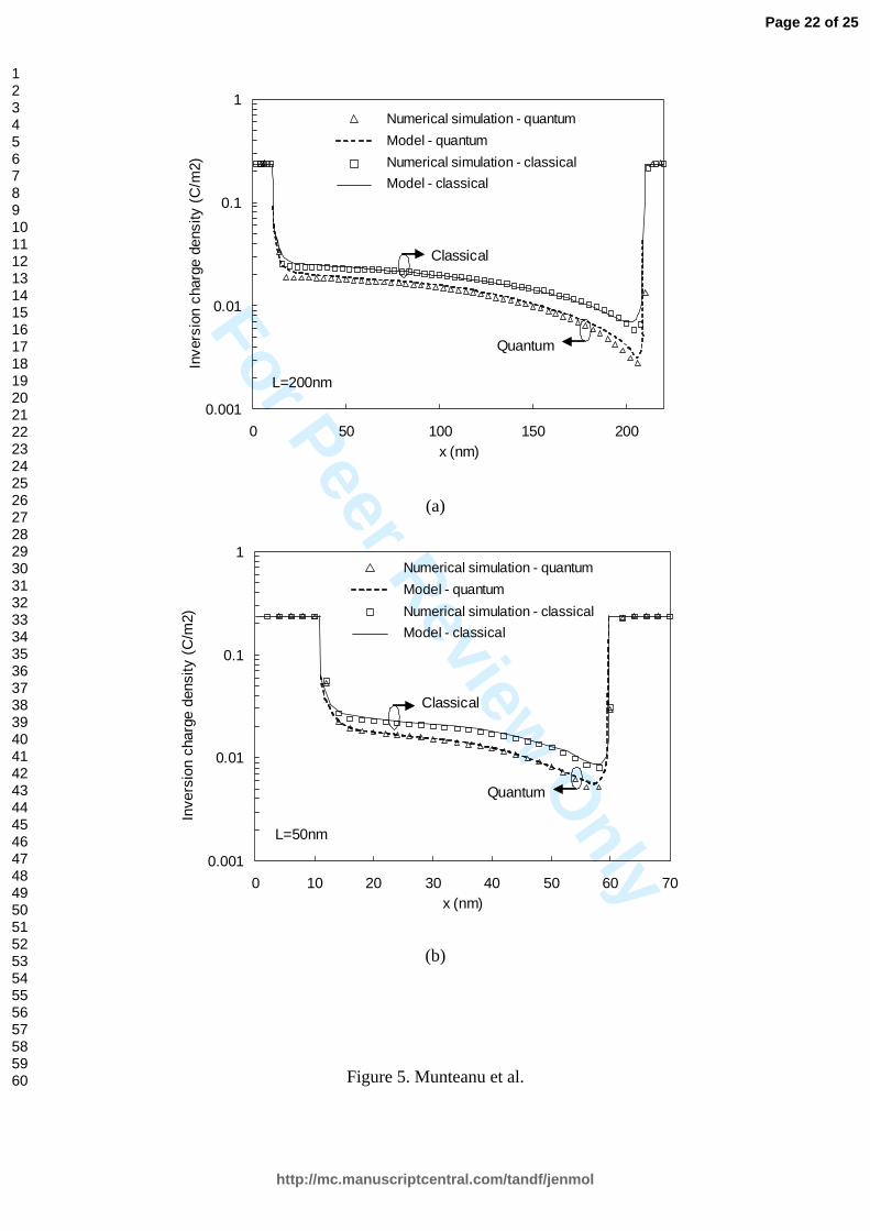
capability to take into account carrier quantization effects. For this purpose the
inversion charge density Qi(x) (in both classical and quantum case) in long and short
channels has been compared to numerical results and very good agreement has been
found (Figure 5). Further the classical and quantum drain current were calculated as a
function of the channel thickness tSi. Figure 6 shows that the quantum model perfectly
reproduces two essential phenomena:
(1) the impact of quantum effects quantum effects, increasingly significant when tSi is
scaled down. The shift between classical and quantum ID(VG) curves increases for
thinner Si channels. In the same way, the shift between the classical and the quantum
threshold voltage is clearly higher for tSi=2nm than that for tSi=10nm.
(2) the drain current dependence on the channel thickness in the subthreshold region, as
a manifestation of the volume inversion, which is a key phenomenon in symmetrical
Page 9 of 25
http://mc.manuscriptcentral.com/tandf/jenmol
123456789101112131415161718192021222324252627282930313233343536373839404142434445464748495051525354555657585960

For Peer Review O
nly
DG transistors. Above threshold the drain current does not depend much on the Si
channel thickness [7].
4. Compact model versus experimental data
Finally, the model was used to fit drain current measured [13-14] on DG devices
(Figure 7). The match between experiment and model is very good, especially in the
subthreshold regime. Above threshold the model slightly overestimates the current due
to the use of a constant mobility and no series resistances. For improving the model
accuracy the next step will be to consider a realistic mobility model [19] and to include
the effect of series resistances.
The proposed compact model can easily be used to obtain all main performance
indicators of DG MOSFET, such as the threshold voltage VT, the subthreshold swing S,
the DIBL (Drain-Induced-Barrier-Lowering) effect on the threshold voltage, the
threshold voltage roll-off, Ion and Ioff currents and the CV/I metric. In addition, the
model can be directly implemented in circuit simulation software and used for the
simulation of DG MOSFET based-circuits, as will be shown in following paragraphe.
5. Model implementation in EldoTM IC analog simulator
The drain current model presented previously has been implemented in a circuit
simulator in order to evaluate the performances of simple DG MOSFET-based circuits.
For this purpose, the model was firstly supplemented by a charge model including the
expressions of charges on the device terminals. The schematic description of the entire
model is given in Figure 8a as well as the symbol of a DG transitor with n-channel. In
this figure QG is the total charge on the two gates, QD is the charge on the drain terminal
and QS is the charge on the source terminal.
Page 10 of 25
http://mc.manuscriptcentral.com/tandf/jenmol
123456789101112131415161718192021222324252627282930313233343536373839404142434445464748495051525354555657585960

For Peer Review O
nly
The starting point for calculating the gate charge is the neutrality condition which
requires that the total charge in the device be always zero:
0QQ IG =+ (24)
In (24) QI is the total inversion charge obtained by the integration of relation (16) from
0 to L:
∫=L
0iI dx)x(QQ (25)
The gate charge QG is then obtained from equation (24). Under normal bias conditions,
the inversion charge is not uniformly distributed along the channel except for VD=VS.
Because of this bias dependence, Qi(x) contributes differently to the source and drain
charges. Various approaches have been proposed for sharing the inversion charge
between the source and drain nodes [20-22]. In our development we have adopted the
approach given in [22] and also presented in [18]. At low drain voltage, the inversion
charge is equally shared between the source and drain. When the drain voltage
increases, the drain charge is strongly reduced and the source charge becomes close to
the inversion charge QI.
It is important to note that our compact model is completely continuous over all
operation regimes and the drain current and node charges equations are derivable and
their derivatives are also continuous over all bias regimes. We have also verified that
the source and the drain electrodes can be permuted.
The compact model described previously for the n-channel DG transistor (NMOS) has
been implemented in Eldo IC simulator. A similar model has been considered for the
DG MOSFET with p-channel (PMOS). The model has been used further to simulate DC
and transient response of a three-stage inverter chain containing DG MOSFETs (the
schematic of this circuit is shown in Figure 8b). The Figure 8c shows the time response
of the two outputs voltages (the output voltage of the second and of the third stages) to a
Page 11 of 25
http://mc.manuscriptcentral.com/tandf/jenmol
123456789101112131415161718192021222324252627282930313233343536373839404142434445464748495051525354555657585960

For Peer Review O
nly
rectangular input voltage. This results demonstrates that the model can be perfectly used
to the simulation of small circuit based on DG MOSFETs.
6. Conclusion
In this paper we developped a compact model for the drain current and node charges in
symmetrical Double-Gate transistors, including short channel and carrier quantization
effects. The model is particularly dedicated to ultra-scaled devices expected at the end-
of-the-roadmap. The starting point of the model was the development of an analytical
expression for the 2D distribution of the potential considering the quantum inversion
charge. An extensive comparison with 2D Poisson-Schrödinger simulation data was
conducted in order to fully validate the model. We have shown that the proposed model
reproduces with an excellent accuracy the impact on the drain current of short channel
effects, volume inversion phenomenon and carrier quantum confinement. A very good
agreement was also obtained with experimental data measured on very integrated
devices. Finally, the model was implemented in Eldo IC analog simulator and the
transient simulation of simple DG CMOS-based circuits has been performed.
7. Acknowledgements
This work was supported by the Network of Excellence SINANO and by the French
National Research Agency (ANR) under the PNANO-MODERN project.
Page 12 of 25
http://mc.manuscriptcentral.com/tandf/jenmol
123456789101112131415161718192021222324252627282930313233343536373839404142434445464748495051525354555657585960

For Peer Review O
nly
References
[1]. Hisamoto D, Short course IEDM Tech Dig 2003 and references therein.
[2]. D.J. Frank et al., "Monte Carlo simulation of a 30nm dual-gate MOSFET: How
short can Si go?", In Proceedings IEDM Tech Dig 1992, p. 553.
[3]. Y. Taur, "Analytic Solutions of Charge and Capacitance in Symmetric and
Asymmetric Double-Gate MOSFETs", IEEE Transactions on Electron Devices,
48(12), p. 2861-2869 (2001).
[4]. M. Chan et al., "Quasi-2D Compact Modeling for Double-Gate MOSFET", in
Proceedings MSM 2004, p. 108-13.
[5]. M. Bescond et al., "Atomic-scale Modeling of Source-to-Drain Tunneling in
Ultimate Schottky Barrier Double-Gate MOSFET’s", in Proceedings ESSDERC, p.
395 (2003).
[6]. M. Bescond et al., "Atomic-scale modeling of Double-Gate MOSFETs using a tight-
binding Green’s function formalism", Solid-State Electronics 48, p. 567 (2004).
[7]. Y. Taur et al., "A Continuous, Analytic Drain-Current Model for DG MOSFETs",
IEEE Electron Device Letters, 25(2), p. 107-109 (2004).
[8]. D. Jiménez et al., "Continuous Analytic I–V Model for Surrounding-Gate
MOSFETs", IEEE Electron Device Letters, 25(8), p. 571-573 (2004).
[9]. A. Ortiz-Conde et al., "Rigorous analytic solution for the drain current of undoped
symmetric dual-gate MOSFETs", Solid State Electronics, 49, p. 640-649 (2005).
[10]. X. Liang and Y. Taur, "A 2-D Analytical Solution for SCEs in DG MOSFETs",
IEEE Transactions on Electron Devices, 51(8), p. 1385-1391 (2004).
[11]. G. Baccarani and S. Reggiani, "A Compact Double-Gate MOSFET Model
Comprising Quantum-Mechanical and Nonstatic Effects", IEEE Transactions on
Electron Devices, 46(8), p. 1656-1666 (1999).
Page 13 of 25
http://mc.manuscriptcentral.com/tandf/jenmol
123456789101112131415161718192021222324252627282930313233343536373839404142434445464748495051525354555657585960
For Peer Review O
nly
[12]. D. Munteanu and J.L. Autran, "Two-dimensional Modeling of Quantum Ballistic
Transport in Ultimate Double-Gate SOI Devices", Solid State Electronics, 47, p.
1219-1225 (2003).
[13]. S. Harrison et al., "Electrical characterization and modeling of high-performance
SON DG MOSFETs", in Proceedings ESSDERC 2004, p. 373-376.
[14]. R. Cerutti et al., "New Design Adapted Planar Double Gate Process for
Performant Low Standby Power Application", in Proceedings Silicon
Nanoworkshop 2005.
[15]. S-H. Oh et al., "Analytic Description of Short-Channel Effects in Fully-Depleted
Double-Gate and Cylindrical, Surrounding-Gate MOSFETs", IEEE Electron
Device Letters, 21(9), p. 445-447 (2000).
[16]. A. Ortiz-Conde et al., "Analytic Solution of the Channel Potential in Undoped
Symmetric Dual-Gate MOSFETs", IEEE Transactions on Electron Devices,
52(7), p. 1669-1672 (2005).
[17]. R.J. Van Overstraeten et al., "Theory of the MOS transistor in weak inversion-
new method to determine the number of surface states", IEEE Transactions on
Electron Devices, 22(5), p. 282-288 (1975).
[18]. X. Loussier et al., "Compact model of drain-current in Double-Gate MOSFETs
including carrier quantization and short-channel effects", in Proceeding MSM
2006.
[19]. M. Alessandrini et al., "Development of an analytical mobility model for the
simulation of ultra-thin single- and double-gate SOI MOSFETs", Solid-State
Electronics, 48, p. 589-595 (2004).
[20]. J.A. Robinson et al., "A general four-terminal charging-current model for the
insulated-gate field-effect transistor—I", Solid-State Electronics, 23, p. 405-410
(1980).
Page 14 of 25
http://mc.manuscriptcentral.com/tandf/jenmol
123456789101112131415161718192021222324252627282930313233343536373839404142434445464748495051525354555657585960

For Peer Review O
nly
[21]. C. Turchetti et al., "On the small-signal behaviour of the MOS transistor in
quasistatic operation", Solid-State Electronics, 26, p. 941-948 (1983).
[22]. Y.P. Tsividis, Operation and modeling of the MOS transistor. 2nd ed. Boston:
McGraw-Hill, 1999.
Page 15 of 25
http://mc.manuscriptcentral.com/tandf/jenmol
123456789101112131415161718192021222324252627282930313233343536373839404142434445464748495051525354555657585960
For Peer Review O
nly
Figure captions
Figure 1. (a) Schematic of symmetrical DG MOSFET structure and its electrical and
geometrical parameters considered in this work; the dashed area shows the closed
surface for the application of the Gauss’s law; (b) Band diagram in a vertical cross-
section in the channel and definition of the different parameters used in the model
development.
Figure 2. (a) Surface potential variation along the channel from source to drain for
L=50nm and L=100nm (tSi=5nm, VD=0.4V). (b) Potential variation the y direction for
differents channel doping levels (tSi=10nm, VG=0.6V). Comparison between compact
model and numerical simulation.
Figure 3. Variation with x of the normalized quasi-Fermi level QFL/VD for L=200nm
(intrinsic channel) at low and high drain voltage.
Figure 4. Drain current in long and short channel DG transistors as calculated by model
in the quatum case and validation by numerical simulation (tSi=10nm, tox=1nm, midgap
gates, intrinsic channel, VD=0.1V).
Figure 5. Variation of the inversion charge density Qi(x) along the channel from source
to drain in the classical and quantum mechanical cases: (a) L=200nm; (b) L=50nm.
Other parameters are: tSi=5nm, VG=1V, VD=0.4V, intrinsic channel.
Figure 6. Impact of film thickness on the subthreshold operation of L=50nm DG
transistor: the model perfectly reproduces quantum effects and volume inversion
Page 16 of 25
http://mc.manuscriptcentral.com/tandf/jenmol
123456789101112131415161718192021222324252627282930313233343536373839404142434445464748495051525354555657585960

For Peer Review O
nly
(tox=1nm, midgap gates, intrinsic channel). The drain current calculated in the classical
case is also shown.
Figure 7. Compact model versus experimental data measured on DG transistors
fabricated with the GAA/SON process described in references [13-14].
Figure 8. (a) Schematic description of the DG model implemented in Eldo IC analog
simulator and definition of the node charges. The symbol of a DG MOSFET with n-
channel is also represented. (b) Schematic of a three-stage inverter chain containing DG
MOSFETs with n- and p-channels. (c) Transient analysis of the three-stages inverter
chain shown in figure (b) and simulated using the model: response to a rectangular input
voltage VIN. The parameters of DG transistors are: L=50nm, tSi=10nm, tox=1.5nm,
intrinsic channel and midgap gates.
Page 17 of 25
http://mc.manuscriptcentral.com/tandf/jenmol
123456789101112131415161718192021222324252627282930313233343536373839404142434445464748495051525354555657585960

For Peer Review O
nly
Source (NSD) Drain (NSD)tSi
L
VD
VG
tox
VG
Gate (φM)
Channel (NA)
ΕS
Ε(x+dx)Ε(x)Ε=0
tSi/2
x
y
0 L x
PE
E1t
E1l
EFS = 0
EFD
A-A
qVD
EFN = qVF(x)EC(x)
A A
qφS
qΨ(x)
EFi(x)
tox
Source (NSD) Drain (NSD)tSi
L
VD
VG
tox
VG
Gate (φM)
Channel (NA)
ΕS
Ε(x+dx)Ε(x)Ε=0
tSi/2
x
y
0 L x
PE
E1t
E1l
EFS = 0
EFD
A-A
qVD
EFN = qVF(x)EC(x)
A A
qφS
qΨ(x)
EFi(x)
tox
Figure 1. Munteanu et al.
(a)
(b)
Page 18 of 25
http://mc.manuscriptcentral.com/tandf/jenmol
123456789101112131415161718192021222324252627282930313233343536373839404142434445464748495051525354555657585960

For Peer Review O
nly
0
0.2
0.4
0.6
0.8
1
1.2
1.4
0 30 60 90 120x (nm)
Numerical simulation - quantumModel - quantum
0V
0.4V
VG=1V
L=50nmSu
rface
pot
entia
l (V)
L=100nm
(a)
0.42
0.44
0.46
0.48
0.5
0 2 4 6 8 10y (nm)
1×1018cm-3
1×1016cm-3
2×1018cm-3
Numerical simulation - quantum
Pote
ntia
l (V)
Model - quantum
(b)
Figure 2. Munteanu et al.
Page 19 of 25
http://mc.manuscriptcentral.com/tandf/jenmol
123456789101112131415161718192021222324252627282930313233343536373839404142434445464748495051525354555657585960

For Peer Review O
nly
0
0.2
0.4
0.6
0.8
1
0 0.05 0.1 0.15 0.2x (nm)
VD=1V
VD=0.1V
Numerical simulation - quantumModel - quantum
0 50 100 150 200
QFL
/ VD
Figure 3. Munteanu et al.
Page 20 of 25
http://mc.manuscriptcentral.com/tandf/jenmol
123456789101112131415161718192021222324252627282930313233343536373839404142434445464748495051525354555657585960

For Peer Review O
nly
0
200
400
600
800
1000
1200
1400
0.2 0.4 0.6 0.8 1
Gate voltage VG (V)
L=30nm
Numerical simulation - quantumModel - quantum
L=50nm
L=200nm
Dra
in c
urre
nt (A
/m)
L=100nm
(a)
0 0.2 0.4 0.6 0.8 1
Gate voltage VG (V)
L=30nm
Numerical simulation - quantumModel - quantum
L=50nm
L=200nm
10-8
10-6
10-4
10-2
104
102
100
Dra
in c
urre
nt (A
/m)
L=100nm
(b)
Figure 4. Munteanu et al.
Page 21 of 25
http://mc.manuscriptcentral.com/tandf/jenmol
123456789101112131415161718192021222324252627282930313233343536373839404142434445464748495051525354555657585960
For Peer Review O
nly
0.001
0.01
0.1
1
0 50 100 150 200x (nm)
L=200nm
Numerical simulation - quantumModel - quantumNumerical simulation - classicalModel - classical
Inve
rsio
n ch
arge
den
sity
(C/m
2)
Quantum
Classical
(a)
0.001
0.01
0.1
1
0 10 20 30 40 50 60 70x (nm)
L=50nm
Numerical simulation - quantumModel - quantumNumerical simulation - classicalModel - classical
Inve
rsio
n ch
arge
den
sity
(C
/m2)
Quantum
Classical
(b)
Figure 5. Munteanu et al.
Page 22 of 25
http://mc.manuscriptcentral.com/tandf/jenmol
123456789101112131415161718192021222324252627282930313233343536373839404142434445464748495051525354555657585960

For Peer Review O
nly
0 0.1 0.2 0.3 0.4 0.5 0.6 0.7
Gate voltage VG (V)
tSi=10nm
tSi=5nm
tSi=2nmL=50nm
10-9
10-7
10-5
10-3
Numerical simulation - quantumModel - quantumNumerical simulation - classicalModel - classical
103
101
10-1
Dra
in c
urre
nt (A
/m)
Figure 6. Munteanu et al.
Page 23 of 25
http://mc.manuscriptcentral.com/tandf/jenmol
123456789101112131415161718192021222324252627282930313233343536373839404142434445464748495051525354555657585960

For Peer Review O
nly
-0.5 0 0.5 1Gate voltage (V)
0.1V
VD=1.2VL=30nmtSi=10nmtox=1.5nm
4×1018cm-3
ExperimentModel - quantum
L=70nmtSi=13.8nmtox=2.2nmIntrinsic channel
0.1V
VD=1.2V
Dra
in c
urre
nt (A
/µm
)
10-11
10-9
10-7
10-5
10-3
10-11
10-9
10-7
10-5
10-3
10-13
10-15
101
10-1
Dra
in c
urre
nt (A
/µm
)
Figure 7. Munteanu et al.
Page 24 of 25
http://mc.manuscriptcentral.com/tandf/jenmol
123456789101112131415161718192021222324252627282930313233343536373839404142434445464748495051525354555657585960

For Peer Review O
nly
VG
L
VD
SourcedxGate oxide
Drain
Gate oxideVS
Si channel
QQGG
QQSS IIDDQQDD
S D
G
G
VG
L
VD
SourcedxGate oxide
Drain
Gate oxideVS
Si channel
QQGG
QQSS IIDDQQDD
VG
L
VD
SourcedxGate oxide
Drain
Gate oxideVS
Si channel
QQGG
QQSS IIDDQQDD
S D
G
G
S D
G
G
(a)
VIN VOUT
VDD
NMOS
PMOS
VDD VDD
V1VIN VOUT
VDD
NMOS
PMOS
VDD
NMOS
PMOS
VDDVDD VDDVDD
V1
(b)
-0.5
0
0.5
1
1.5
0 5 10 15 20 25 30 35 40Time (ps)
Out
put v
olta
ge (V
)
V1
VOUT
(c)
Figure 8. Munteanu et al.
Page 25 of 25
http://mc.manuscriptcentral.com/tandf/jenmol
123456789101112131415161718192021222324252627282930313233343536373839404142434445464748495051525354555657585960