Embed Size (px)
Citation preview
HAL Id: tel-02124585https://tel.archives-ouvertes.fr/tel-02124585
Submitted on 9 May 2019
HAL is a multi-disciplinary open accessarchive for the deposit and dissemination of sci-entific research documents, whether they are pub-lished or not. The documents may come fromteaching and research institutions in France orabroad, or from public or private research centers.
L’archive ouverte pluridisciplinaire HAL, estdestinée au dépôt et à la diffusion de documentsscientifiques de niveau recherche, publiés ou non,émanant des établissements d’enseignement et derecherche français ou étrangers, des laboratoirespublics ou privés.
Contribution to the study of the SiC MOSFETs gateoxide
Oriol Aviñó Salvadó
To cite this version:Oriol Aviñó Salvadó. Contribution to the study of the SiC MOSFETs gate oxide. Electronics. Uni-versité de Lyon, 2018. English. NNT : 2018LYSEI110. tel-02124585
N°d’ordre NNT : 2018LYSEI110
THESE de DOCTORAT DE L’UNIVERSITE DE LYON
opérée au sein de
INSA de Lyon
Ecole Doctorale N° EDA160 Électronique, Électrotechnique, Automatique de Lyon
Spécialité de doctorat : Génie Électrique
Soutenue publiquement le 14/12/2018, par :
Oriol Aviñó Salvadó
Contribution to the Study of the SiC MOSFETs Gate Oxide
Devant le jury composé de :
IANNUZZO, Francesco Prof. Université Aalborg Universitet Rapporteur
CASTELLAZZI, Alberto Associate Professor Nottingham University Rapporteur
LEFEBVRE, Stéphane Prof. Université CNAM Examinateur
MALBERT, Nathalie Prof. Université IMS Examinatrice
MOREL, Hervé Directeur de Recherche CNRS Directeur de thèse
BUTTAY, Cyril Chargé de Recherche CNRS Co-Directeur de thèse
Cette thèse est accessible à l'adresse : http://theses.insa-lyon.fr/publication/2018LYSEI110/these.pdf © [O. Aviñó Salvadó], [2018], INSA Lyon, tous droits réservés

Cette thèse est accessible à l'adresse : http://theses.insa-lyon.fr/publication/2018LYSEI110/these.pdf © [O. Aviñó Salvadó], [2018], INSA Lyon, tous droits réservés

Département FEDORA – INSA Lyon - Ecoles Doctorales – Quinquennal 2016-2020
SIGLE ECOLE DOCTORALE NOM ET COORDONNEES DU RESPONSABLE
CHIMIE
CHIMIE DE LYON http://www.edchimie-lyon.fr
Sec : Renée EL MELHEM Bat Blaise Pascal 3e etage [email protected] Insa : R. GOURDON
M. Stéphane DANIELE Institut de Recherches sur la Catalyse et l'Environnement de Lyon IRCELYON-UMR 5256 Équipe CDFA 2 avenue Albert Einstein 69626 Villeurbanne cedex [email protected]
E.E.A.
ELECTRONIQUE, ELECTROTECHNIQUE, AUTOMATIQUE http://edeea.ec-lyon.fr
Sec : M.C. HAVGOUDOUKIAN [email protected]
M. Gérard SCORLETTI Ecole Centrale de Lyon 36 avenue Guy de Collongue 69134 ECULLY Tél : 04.72.18 60.97 Fax : 04 78 43 37 17 [email protected]
E2M2
EVOLUTION, ECOSYSTEME, MICROBIOLOGIE, MODELISATION http://e2m2.universite-lyon.fr
Sec : Sylvie ROBERJOT Bât Atrium - UCB Lyon 1
04.72.44.83.62 Insa : H. CHARLES [email protected]
M. Fabrice CORDEY CNRS UMR 5276 Lab. de géologie de Lyon Université Claude Bernard Lyon 1 Bât Géode 2 rue Raphaël Dubois 69622 VILLEURBANNE Cédex Tél : 06.07.53.89.13 cordey@ univ-lyon1.fr
EDISS
INTERDISCIPLINAIRE SCIENCES- SANTE http://www.ediss-lyon.fr
Sec : Sylvie ROBERJOT Bât Atrium - UCB Lyon 1
04.72.44.83.62 Insa : M. LAGARDE [email protected]
Mme Emmanuelle CANET-SOULAS INSERM U1060, CarMeN lab, Univ. Lyon 1 Bâtiment IMBL 11 avenue Jean Capelle INSA de Lyon 696621 Villeurbanne Tél : 04.72.68.49.09 Fax :04 72 68 49 16 [email protected]
INFOMATHS
INFORMATIQUE ET MATHEMATIQUES http://infomaths.univ-lyon1.fr
Sec :Renée EL MELHEM Bat Blaise Pascal 3e etage [email protected]
Mme Sylvie CALABRETTO LIRIS – INSA de Lyon Bat Blaise Pascal 7 avenue Jean Capelle 69622 VILLEURBANNE Cedex Tél : 04.72. 43. 80. 46 Fax 04 72 43 16 87 [email protected]
Matériaux
MATERIAUX DE LYON http://ed34.universite-lyon.fr
Sec : M. LABOUNE PM : 71.70 –Fax : 87.12 Bat. Direction [email protected]
M. Jean-Yves BUFFIERE INSA de Lyon MATEIS Bâtiment Saint Exupéry 7 avenue Jean Capelle 69621 VILLEURBANNE Cedex Tél : 04.72.43 71.70 Fax 04 72 43 85 28 [email protected]
MEGA
MECANIQUE, ENERGETIQUE, GENIE CIVIL, ACOUSTIQUE http://mega.universite-lyon.fr
Sec : M. LABOUNE PM : 71.70 –Fax : 87.12 Bat. Direction [email protected]
M. Philippe BOISSE INSA de Lyon Laboratoire LAMCOS Bâtiment Jacquard 25 bis avenue Jean Capelle 69621 VILLEURBANNE Cedex Tél : 04.72 .43.71.70 Fax : 04 72 43 72 37 [email protected]
ScSo
ScSo* http://recherche.univ-lyon2.fr/scso/
Sec : Viviane POLSINELLI
Brigitte DUBOIS Insa : J.Y. TOUSSAINT Tél : 04 78 69 72 76 [email protected]
M. Christian MONTES Université Lyon 2 86 rue Pasteur 69365 LYON Cedex 07 [email protected]
*ScSo : Histoire, Géographie, Aménagement, Urbanisme, Archéologie, Science politique, Sociologie, Anthropologie
Cette thèse est accessible à l'adresse : http://theses.insa-lyon.fr/publication/2018LYSEI110/these.pdf © [O. Aviñó Salvadó], [2018], INSA Lyon, tous droits réservés

Cette thèse est accessible à l'adresse : http://theses.insa-lyon.fr/publication/2018LYSEI110/these.pdf © [O. Aviñó Salvadó], [2018], INSA Lyon, tous droits réservés
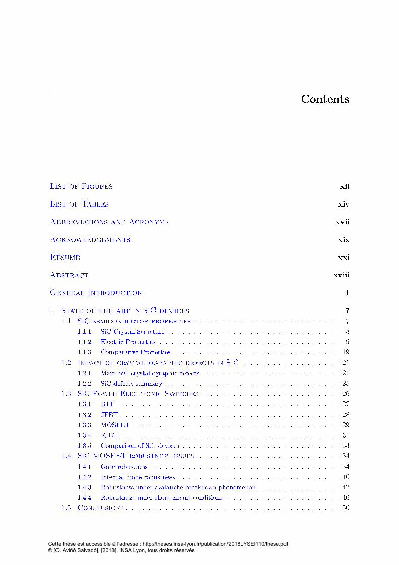
Contents
List of Figures xii
List of Tables xiv
Abbreviations and Acronyms xvii
Acknowledgements xix
Résumé xxi
Abstract xxiii
General Introduction 1
1 State of the art in SiC devices 7
1.1 SiC semiconductor properties . . . . . . . . . . . . . . . . . . . . . . . . . 7
1.1.1 SiC Crystal Structure . . . . . . . . . . . . . . . . . . . . . . . . . . . . . 8
1.1.2 Electric Properties . . . . . . . . . . . . . . . . . . . . . . . . . . . . . . . 9
1.1.3 Comparative Properties . . . . . . . . . . . . . . . . . . . . . . . . . . . . 19
1.2 Impact of crystallographic defects in SiC . . . . . . . . . . . . . . . . 21
1.2.1 Main SiC crystallographic defects . . . . . . . . . . . . . . . . . . . . . . . 21
1.2.2 SiC defects summary . . . . . . . . . . . . . . . . . . . . . . . . . . . . . . 25
1.3 SiC Power Electronic Switches . . . . . . . . . . . . . . . . . . . . . . . 26
1.3.1 BJT . . . . . . . . . . . . . . . . . . . . . . . . . . . . . . . . . . . . . . 27
1.3.2 JFET . . . . . . . . . . . . . . . . . . . . . . . . . . . . . . . . . . . . . . 28
1.3.3 MOSFET . . . . . . . . . . . . . . . . . . . . . . . . . . . . . . . . . . . 29
1.3.4 IGBT . . . . . . . . . . . . . . . . . . . . . . . . . . . . . . . . . . . . . . 31
1.3.5 Comparison of SiC devices . . . . . . . . . . . . . . . . . . . . . . . . . . . 33
1.4 SiC MOSFET robustness issues . . . . . . . . . . . . . . . . . . . . . . . . 34
1.4.1 Gate robustness . . . . . . . . . . . . . . . . . . . . . . . . . . . . . . . . 34
1.4.2 Internal diode robustness . . . . . . . . . . . . . . . . . . . . . . . . . . . . 40
1.4.3 Robustness under avalanche breakdown phenomenon . . . . . . . . . . . . . 42
1.4.4 Robustness under short-circuit conditions . . . . . . . . . . . . . . . . . . . 46
1.5 Conclusions . . . . . . . . . . . . . . . . . . . . . . . . . . . . . . . . . . . . . 50
Cette thèse est accessible à l'adresse : http://theses.insa-lyon.fr/publication/2018LYSEI110/these.pdf © [O. Aviñó Salvadó], [2018], INSA Lyon, tous droits réservés
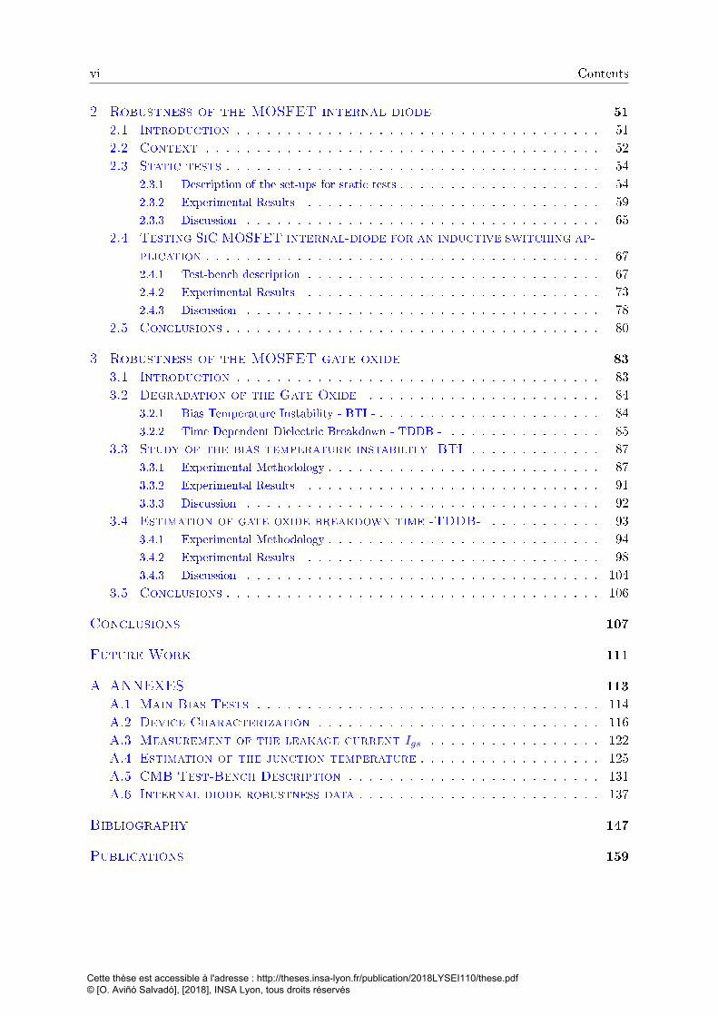
vi Contents
2 Robustness of the MOSFET internal diode 51
2.1 Introduction . . . . . . . . . . . . . . . . . . . . . . . . . . . . . . . . . . . . 512.2 Context . . . . . . . . . . . . . . . . . . . . . . . . . . . . . . . . . . . . . . . 522.3 Static tests . . . . . . . . . . . . . . . . . . . . . . . . . . . . . . . . . . . . . 54
2.3.1 Description of the set-ups for static tests . . . . . . . . . . . . . . . . . . . . 542.3.2 Experimental Results . . . . . . . . . . . . . . . . . . . . . . . . . . . . . 592.3.3 Discussion . . . . . . . . . . . . . . . . . . . . . . . . . . . . . . . . . . . 65
2.4 Testing SiC MOSFET internal-diode for an inductive switching ap-
plication . . . . . . . . . . . . . . . . . . . . . . . . . . . . . . . . . . . . . . . 672.4.1 Test-bench description . . . . . . . . . . . . . . . . . . . . . . . . . . . . . 672.4.2 Experimental Results . . . . . . . . . . . . . . . . . . . . . . . . . . . . . 732.4.3 Discussion . . . . . . . . . . . . . . . . . . . . . . . . . . . . . . . . . . . 78
2.5 Conclusions . . . . . . . . . . . . . . . . . . . . . . . . . . . . . . . . . . . . . 80
3 Robustness of the MOSFET gate oxide 83
3.1 Introduction . . . . . . . . . . . . . . . . . . . . . . . . . . . . . . . . . . . . 833.2 Degradation of the Gate Oxide . . . . . . . . . . . . . . . . . . . . . . . 84
3.2.1 Bias Temperature Instability - BTI - . . . . . . . . . . . . . . . . . . . . . . 843.2.2 Time Dependent Dielectric Breakdown - TDDB - . . . . . . . . . . . . . . . 85
3.3 Study of the bias temperature instability -BTI- . . . . . . . . . . . . . 873.3.1 Experimental Methodology . . . . . . . . . . . . . . . . . . . . . . . . . . . 873.3.2 Experimental Results . . . . . . . . . . . . . . . . . . . . . . . . . . . . . 913.3.3 Discussion . . . . . . . . . . . . . . . . . . . . . . . . . . . . . . . . . . . 92
3.4 Estimation of gate oxide breakdown time -TDDB- . . . . . . . . . . . 933.4.1 Experimental Methodology . . . . . . . . . . . . . . . . . . . . . . . . . . . 943.4.2 Experimental Results . . . . . . . . . . . . . . . . . . . . . . . . . . . . . 983.4.3 Discussion . . . . . . . . . . . . . . . . . . . . . . . . . . . . . . . . . . . 104
3.5 Conclusions . . . . . . . . . . . . . . . . . . . . . . . . . . . . . . . . . . . . . 106
Conclusions 107
Future Work 111
A ANNEXES 113
A.1 Main Bias Tests . . . . . . . . . . . . . . . . . . . . . . . . . . . . . . . . . . 114A.2 Device Characterization . . . . . . . . . . . . . . . . . . . . . . . . . . . . 116A.3 Measurement of the leakage current Igs . . . . . . . . . . . . . . . . . 122A.4 Estimation of the junction temperature . . . . . . . . . . . . . . . . . . 125A.5 CMB Test-Bench Description . . . . . . . . . . . . . . . . . . . . . . . . . 131A.6 Internal diode robustness data . . . . . . . . . . . . . . . . . . . . . . . . 137
Bibliography 147
Publications 159
Cette thèse est accessible à l'adresse : http://theses.insa-lyon.fr/publication/2018LYSEI110/these.pdf © [O. Aviñó Salvadó], [2018], INSA Lyon, tous droits réservés
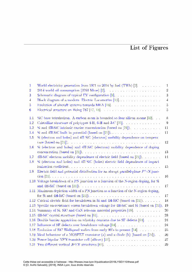
List of Figures
1 World electricity generation from 1971 to 2014 by fuel (TWh) [2]. . . . . . . . 12 2014 world oil consumption (3761 Mtoe) [2]. . . . . . . . . . . . . . . . . . . . 23 Schematic diagram of typical EV conguration [9]. . . . . . . . . . . . . . . . . 34 Block diagram of a modern Electric Locomotive [13]. . . . . . . . . . . . . . . . 45 Evolution of aircraft systems towards MEA [16]. . . . . . . . . . . . . . . . . . 56 Electrical structure on Boing 787 [17, 18]. . . . . . . . . . . . . . . . . . . . . . 5
1.1 SiC base tetrahedron. A carbon atom is bounded to four silicon atoms [32]. . . 81.2 Cristalline structure of polytypes 4-H, 6-H and 3-C [35]. . . . . . . . . . . . . . 91.3 Si and 4H-SiC intrinsic carrier concentration (based on [21]). . . . . . . . . . . 111.4 Si and 4H-SiC built-in potential (based on [21]). . . . . . . . . . . . . . . . . . . 111.5 Si (electron and holes) and 4H-SiC (electron) mobility dependence on tempera-
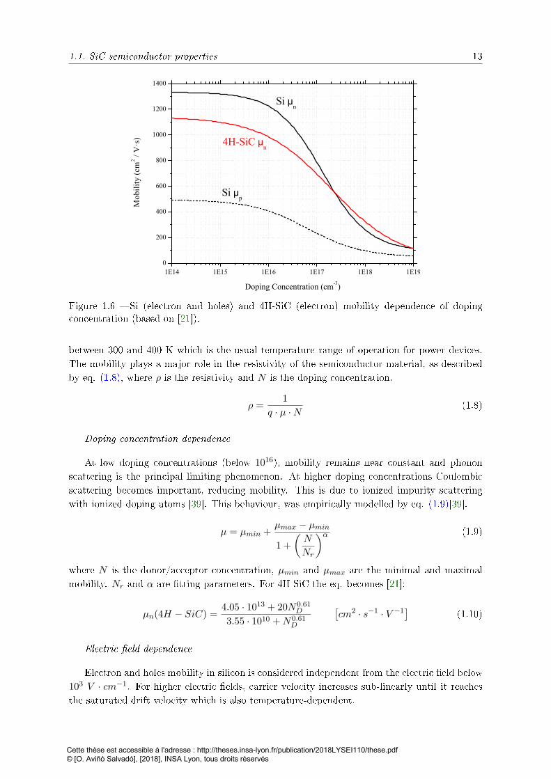
ture (based on [21]). . . . . . . . . . . . . . . . . . . . . . . . . . . . . . . . . . 121.6 Si (electron and holes) and 4H-SiC (electron) mobility dependence of doping
concentration (based on [21]). . . . . . . . . . . . . . . . . . . . . . . . . . . . . 131.7 4H-SiC electron mobility dependence of electric eld (based on [21]). . . . . . . 141.8 Si (electron and holes) and 4H-SiC (holes) electric eld dependence of impact
ionization coecient. . . . . . . . . . . . . . . . . . . . . . . . . . . . . . . . . . 151.9 Electric eld and potential distribution for an abrupt parallel-plane P+-N junc-
tion [21]. . . . . . . . . . . . . . . . . . . . . . . . . . . . . . . . . . . . . . . . . 161.10 Voltage breakdown of a PN junction as a function of the N-region doping, for Si
and 4H-SiC (based on [21]). . . . . . . . . . . . . . . . . . . . . . . . . . . . . . 171.11 Maximum depletion width of a PN junction as a function of the N-region doping,
for Si and 4H-SiC (based on [21]). . . . . . . . . . . . . . . . . . . . . . . . . . . 171.12 Critical electric eld for breakdown in Si and 4H-SiC (based on [21]). . . . . . . 181.13 Specic on-resistance versus breakdown voltage for 4H-SiC and Si (based on [21]). 191.14 Summary of Si, SiC and GaN relevant material properties [48]. . . . . . . . . . 201.15 4H-SiC crystal structure (based on [61]. . . . . . . . . . . . . . . . . . . . . . . 231.16 Double barrier apparition on schottky contacts due to SF defects [64]. . . . . . 241.17 Inuence of SF defects over breakdown voltage [64]. . . . . . . . . . . . . . . . . 241.18 Evolution of SiC Wolfspeed wafers from early 90's to present [54]. . . . . . . . . 251.19 Ideal behaviour of a MOSFET transistor (a) and a diode (b) (based on [70]). . 261.20 Power bipolar NPN transistor cell (silicon) [21]. . . . . . . . . . . . . . . . . . . 271.21 Two dierent vertical JFET structures [81]. . . . . . . . . . . . . . . . . . . . . 29
Cette thèse est accessible à l'adresse : http://theses.insa-lyon.fr/publication/2018LYSEI110/these.pdf © [O. Aviñó Salvadó], [2018], INSA Lyon, tous droits réservés
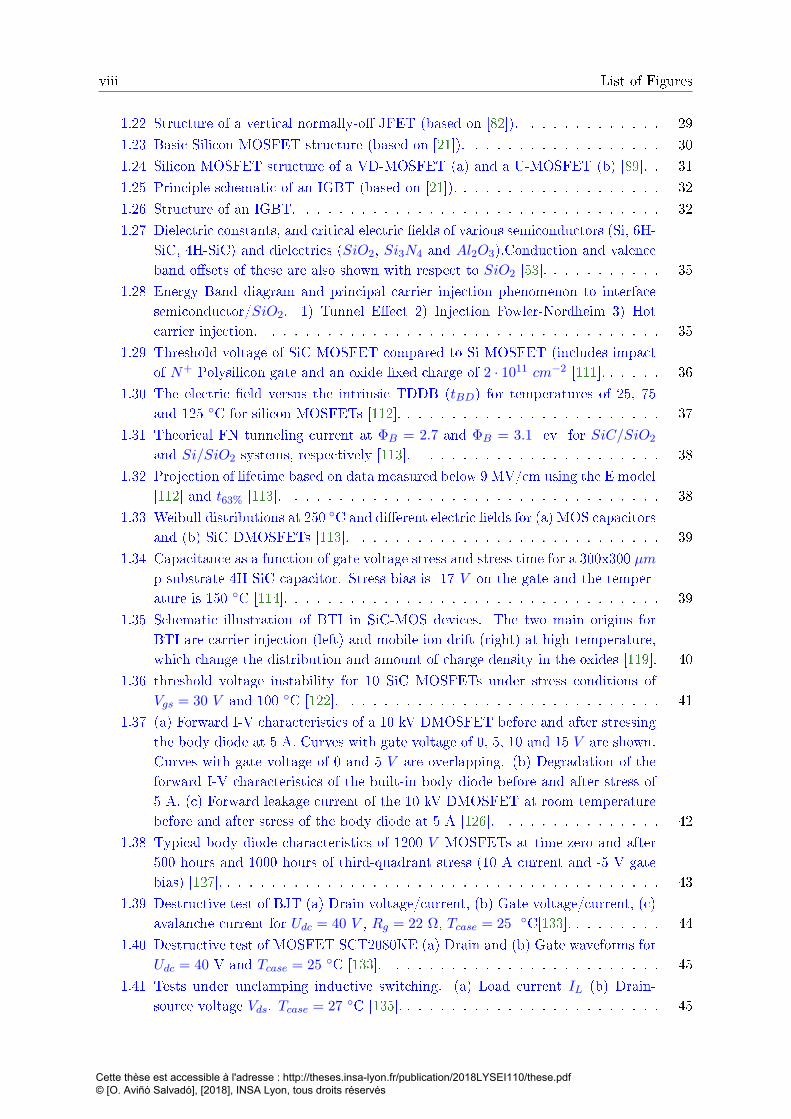
viii List of Figures
1.22 Structure of a vertical normally-o JFET (based on [82]). . . . . . . . . . . . . 29
1.23 Basic Silicon MOSFET structure (based on [21]). . . . . . . . . . . . . . . . . . 30
1.24 Silicon MOSFET structure of a VD-MOSFET (a) and a U-MOSFET (b) [89]. . 31
1.25 Principle schematic of an IGBT (based on [21]). . . . . . . . . . . . . . . . . . . 32
1.26 Structure of an IGBT. . . . . . . . . . . . . . . . . . . . . . . . . . . . . . . . . 32
1.27 Dielectric constants, and critical electric elds of various semiconductors (Si, 6H-SiC, 4H-SiC) and dielectrics (SiO2, Si3N4 and Al2O3).Conduction and valenceband osets of these are also shown with respect to SiO2 [53]. . . . . . . . . . . 35
1.28 Energy Band diagram and principal carrier injection phenomenon to interfacesemiconductor/SiO2. 1) Tunnel Eect 2) Injection Fowler-Nordheim 3) Hotcarrier injection. . . . . . . . . . . . . . . . . . . . . . . . . . . . . . . . . . . . 35
1.29 Threshold voltage of SiC MOSFET compared to Si MOSFET (includes impactof N+ Polysilicon gate and an oxide xed charge of 2 · 1011 cm−2 [111]. . . . . . 36
1.30 The electric eld versus the intrinsic TDDB (tBD) for temperatures of 25, 75and 125 C for silicon MOSFETs [112]. . . . . . . . . . . . . . . . . . . . . . . . 37
1.31 Theorical FN tunneling current at ΦB = 2.7 and ΦB = 3.1 ev for SiC/SiO2
and Si/SiO2 systems, respectively [113]. . . . . . . . . . . . . . . . . . . . . . 38
1.32 Projection of lifetime based on data measured below 9 MV/cm using the E model[112] and t63% [113]. . . . . . . . . . . . . . . . . . . . . . . . . . . . . . . . . . 38
1.33 Weibull distributions at 250 C and dierent electric elds for (a) MOS capacitorsand (b) SiC DMOSFETs [113]. . . . . . . . . . . . . . . . . . . . . . . . . . . . 39
1.34 Capacitance as a function of gate voltage stress and stress time for a 300x300 µmp-substrate 4H-SiC capacitor. Stress bias is -17 V on the gate and the temper-ature is 150 C [114]. . . . . . . . . . . . . . . . . . . . . . . . . . . . . . . . . . 39
1.35 Schematic illustration of BTI in SiC-MOS devices. The two main origins forBTI are carrier injection (left) and mobile ion drift (right) at high temperature,which change the distribution and amount of charge density in the oxides [119]. 40
1.36 threshold voltage instability for 10 SiC MOSFETs under stress conditions ofVgs = 30 V and 100 C [122]. . . . . . . . . . . . . . . . . . . . . . . . . . . . . 41
1.37 (a) Forward I-V characteristics of a 10 kV DMOSFET before and after stressingthe body diode at 5 A. Curves with gate voltage of 0, 5, 10 and 15 V are shown.Curves with gate voltage of 0 and 5 V are overlapping. (b) Degradation of theforward I-V characteristics of the built-in body diode before and after stress of5 A. (c) Forward leakage current of the 10 kV DMOSFET at room temperaturebefore and after stress of the body diode at 5 A [126]. . . . . . . . . . . . . . . 42
1.38 Typical body diode characteristics of 1200 V MOSFETs at time-zero and after500 hours and 1000 hours of third-quadrant stress (10 A current and -5 V gatebias) [127]. . . . . . . . . . . . . . . . . . . . . . . . . . . . . . . . . . . . . . . . 43
1.39 Destructive test of BJT (a) Drain voltage/current, (b) Gate voltage/current, (c)avalanche current for Udc = 40 V , Rg = 22 Ω, Tcase = 25 C[133]. . . . . . . . . 44
1.40 Destructive test of MOSFET SCT2080KE (a) Drain and (b) Gate waveforms forUdc = 40 V and Tcase = 25 C [133]. . . . . . . . . . . . . . . . . . . . . . . . . 45
1.41 Tests under unclamping inductive switching. (a) Load current IL (b) Drain-source voltage Vds. Tcase = 27 C [135]. . . . . . . . . . . . . . . . . . . . . . . . 45
Cette thèse est accessible à l'adresse : http://theses.insa-lyon.fr/publication/2018LYSEI110/these.pdf © [O. Aviñó Salvadó], [2018], INSA Lyon, tous droits réservés
List of Figures ix
1.42 Simulation of the gate-source voltage Vgs and gate-source current Igs behaviourunder short circuit event [111]. . . . . . . . . . . . . . . . . . . . . . . . . . . . 46
1.43 Structures of Si and SiC MOSFETs (a) Planar MOSFET structure (b) Shieldedplanar MOSFET structure [111]. . . . . . . . . . . . . . . . . . . . . . . . . . . 47
1.44 Reduction in gate-source voltage for planar SiC MOSFET and Shield planar SiCMOSFET [111]. . . . . . . . . . . . . . . . . . . . . . . . . . . . . . . . . . . . . 47
1.45 Id short-circuit waveforms (Vds = 400 V , Vgs = 18 V , Tcase = 27 C, CREE)[137]. . . . . . . . . . . . . . . . . . . . . . . . . . . . . . . . . . . . . . . . . . . 48
2.1 Typical forward current-voltage characteristics of pn-junction-based body diodein a conventional SiC MOSFET after applying forward current of 15 A [145](2016). . . . . . . . . . . . . . . . . . . . . . . . . . . . . . . . . . . . . . . . . . 52
2.2 Typical data of Vth shift after the application of an HTGB test (a) positivebias stress Vgs=20 V (b)negative bias stress Vgs=-10 V over 1000 hours at150 C [145] (2016). . . . . . . . . . . . . . . . . . . . . . . . . . . . . . . . . . 53
2.3 Typical SiC NMOSFET cross section and its parasitic elements. IBD and ICHrefers to current owing through the body diode and channel paths, respectively. 53
2.4 1st order MOSFET steady-state thermal model . . . . . . . . . . . . . . . . . . 55
2.5 Biasing conditions for the measurement of Isat = f(T ) characterization. . . . . 55
2.6 DUT assembled within the hot-plate. . . . . . . . . . . . . . . . . . . . . . . . . 56
2.7 HTGB JEDEC Test . . . . . . . . . . . . . . . . . . . . . . . . . . . . . . . . . 57
2.8 Set of realized static tests . . . . . . . . . . . . . . . . . . . . . . . . . . . . . . 58
2.9 Rds characterization at 150 C on a Wolfspeed C2M008012D MOSFET . . . . . 59
2.10 Rds-on evolution for HTGB test. Characterised at room temperature, Ids = 10 Aand Vgs = 20 V . . . . . . . . . . . . . . . . . . . . . . . . . . . . . . . . . . . . . 60
2.11 Intrinsic diode forward voltage evolution for HTGB test. Characterised at roomtemperature, If = 10 A and Vgs = −8 V . . . . . . . . . . . . . . . . . . . . . . 60
2.12 Threshold voltage evolution for HTGB test. Characterised at room temperature,Ids = 100 µA and Vds = 1 V . . . . . . . . . . . . . . . . . . . . . . . . . . . . . 61
2.13 Rds evolution (3 samples). Test conditions (table 2.1): 1Q and 4Q (ICH =
16 A, Vgs = 20 V ); 3Q (IBD = 10 A, Vgs = −8 V ). Characterised at 150 C,Ids = 10 A and Vgs = 20 V . . . . . . . . . . . . . . . . . . . . . . . . . . . . . . 62
2.14 Vf evolution (3 samples). Test conditions (table 2.1): 1Q and 4Q (ICH =
16 A, Vgs = 20 V ); 3Q (IBD = 10 A, Vgs = −8 V ). Characterised at 150 C,If = 10 A and Vgs = −8 V . . . . . . . . . . . . . . . . . . . . . . . . . . . . . . 63
2.15 Vth evolution (3 samples). Test conditions (table 2.1): 1Q and 4Q (ICH =
16 A, Vgs = 20 V ); 3Q (IBD = 10 A, Vgs = −8 V ). Characterised at 150 C,Ids = 100 µA and Vds = 1 V . . . . . . . . . . . . . . . . . . . . . . . . . . . . . 64
2.16 Vth evolution and extrapolation for 3 samples operating in the 3Q:(IBD = 10 A)for Vgs = −5 and Vgs = −8 V . Characterised at 150 C, Ids = 100 µA andVds = 1 V . . . . . . . . . . . . . . . . . . . . . . . . . . . . . . . . . . . . . . . . 65
2.17 Schematic of the back to back test-bench (CMB). . . . . . . . . . . . . . . . . . 68
2.18 Simplied CMB schematic, modelling the boost converter as a continuous currentsource. . . . . . . . . . . . . . . . . . . . . . . . . . . . . . . . . . . . . . . . . . 69
Cette thèse est accessible à l'adresse : http://theses.insa-lyon.fr/publication/2018LYSEI110/these.pdf © [O. Aviñó Salvadó], [2018], INSA Lyon, tous droits réservés

x List of Figures
2.19 Qualitative waveforms of current and voltage for the DUT, as well as the logicstates for switches M1 and DUT. Body diode current is plotted in blue. Whenit ows through the channel, it is plotted in red. . . . . . . . . . . . . . . . . . . 71
2.20 Normalized evolution of Rds, Vf and Vth for CMB test (DUT always blocked atVgs = −8 V ). Characterizations realized at room temperature. . . . . . . . . . . 74
2.21 Evolution and extrapolation of normalized Vth over CMB test stress. Character-ization at ambient temperature, Ids = 100 µA, Vds = 1 V . . . . . . . . . . . . . 75
2.22 Comparison of normalized Rds, Vf and Vth evolution for CMB1 test for dierentmanufacturers (ROHM, ST, Wolfspeed). Characterizations realized at roomtemperature. . . . . . . . . . . . . . . . . . . . . . . . . . . . . . . . . . . . . . 76
2.23 Evolution of normalized Vth over CMB test stress for CMB1 and CMB2 test-bench (Vgs = −8 V ). Characterization at ambient temperature, Ids = 100 µA,Vds = 1 V . . . . . . . . . . . . . . . . . . . . . . . . . . . . . . . . . . . . . . . . 77
2.24 Evolution of normalized Vth over CMB test stress (test-bench CMB2, Vgs =
−5 V ) for three samples. Characterization at ambient temperature, Ids =
100 µA, Vds = 1 V . . . . . . . . . . . . . . . . . . . . . . . . . . . . . . . . . . . 77
2.25 Normalized evolution of Rds, Vf and Vth for CMB1 test for dierent duty cycles(D). Characterizations realized at room temperature. . . . . . . . . . . . . . . . 78
2.26 Comparison between results obtained from CMB tests stress and from statictest (3rd quadrant) for two dierent gate-source voltages (Vgs = −8 V andVgs = −5 V ). For CMB tests, the internal diode is only biased 50% of the testtime. . . . . . . . . . . . . . . . . . . . . . . . . . . . . . . . . . . . . . . . . . . 79
3.1 Evolution of Vth for HTGB tests at Vgs=20 V , Vgs=-10 V and Vgs=-5 V [123]. . 84
3.2 Electric eld in the gate oxide depending on the gate-source and drain-sourcevoltage [160]. . . . . . . . . . . . . . . . . . . . . . . . . . . . . . . . . . . . . . 86
3.3 Estimation of TDDB at 150 C for Gen2 CREE MOSFETs [127]. . . . . . . . . 86
3.4 Estimation of TDDB depending on temperature for Gen1 CREE MOSFETscommanding a resistive charge [82]. . . . . . . . . . . . . . . . . . . . . . . . . . 87
3.5 Main circuit congurations for the preliminary tests. . . . . . . . . . . . . . . . 88
3.6 Temperature prole used for the preliminary tests. . . . . . . . . . . . . . . . . 89
3.7 Conguration used for HTGB tests over 1000 hours (Cong 3). . . . . . . . . . 89
3.8 Evolution of Vth for realized preliminary tests and the used temperature prole. 90
3.9 Evolution of normalized Vth and Igs for HTGB test conditions (Vgs=22 V ,Vds=0 V , Tj = 150 C) for 4 Wolfspeed C2M0080120D samples. . . . . . . . . . 91
3.10 Evolution of normalized Vth and Igs for HTGB test conditions (Vgs=22 V ,Vds=0 V , Tj = 200 C) for 4 Wolfspeed C2M0080120D samples. . . . . . . . . 92
3.11 Evolution of normalized Vth and Igs for HTGB test conditions (Vgs=22 V ,Vds=0 V , Tj = 200 C) over samples of three dierent manufacturers (ST,ROHM, Wolfspeed). . . . . . . . . . . . . . . . . . . . . . . . . . . . . . . . . . 93
3.12 Circuit conguration used for the static stress of the gate oxide. . . . . . . . . . 95
3.13 Simplied schematic of the test-bench used for the inductive switching stress testof the gate oxide. . . . . . . . . . . . . . . . . . . . . . . . . . . . . . . . . . . . 97
3.14 Igs (Vgs) characterization on 10 C2M0080120D Wolfspeed samples. . . . . . . . 98
3.15 TDDB estimation for static tests at Tj = 150 C. . . . . . . . . . . . . . . . . . 99
Cette thèse est accessible à l'adresse : http://theses.insa-lyon.fr/publication/2018LYSEI110/these.pdf © [O. Aviñó Salvadó], [2018], INSA Lyon, tous droits réservés
List of Figures xi
3.16 Evolution of Igs at Tj = 150 C during the static tests for several Vgs levels. . . 100
3.17 Injected charge during the static tests for several Vgs levels, Tj = 150 C. . . . . 100
3.18 Comparison between the two failure types (suddent and progressive) at 150 C. 101
3.19 Igs measurement until failure apparition at Vgs=42.5 V during a static stress atTj = 150 C, which is interrupted regularly to re-characterize the device. . . . . 102
3.20 Cgs evolution during the static stress at Vgs=42.5 V . Characterized at roomtemperature. . . . . . . . . . . . . . . . . . . . . . . . . . . . . . . . . . . . . . 102
3.21 Ids−Vgs evolution during the static stress at Vgs=42.5 V . Characterized at roomtemperature and Vds=1 V . . . . . . . . . . . . . . . . . . . . . . . . . . . . . . . 103
3.22 TDDB estimation for a SiC MOSFET placed in a DC/DC converter at Tj = 150 C.104
3.23 Expected lifetimes depending on Vgs. Comparison between Wolfspeed data andthe experimental data (obtained from inductive commutation tests as well asstatic tests. . . . . . . . . . . . . . . . . . . . . . . . . . . . . . . . . . . . . . . 105
A.1 Connection box used for the characterization of Ids − Vds, Vf and Vth curves. . 116
A.2 Setup used for the measurement of Ids − Vds characteristics. . . . . . . . . . . . 117
A.3 Typical Ids−Vds characteristic curves of a SiC MOSFET for dierent gate-sourcevoltages. . . . . . . . . . . . . . . . . . . . . . . . . . . . . . . . . . . . . . . . . 117
A.4 Setup used for the measurement of Vf -Ids. . . . . . . . . . . . . . . . . . . . . . 118
A.5 Typical Vf (-Vds) characteristic of a SiC MOSFET for dierent gate-source voltages.118
A.6 Setup used for the measurement of Vth. . . . . . . . . . . . . . . . . . . . . . . . 119
A.7 Ids − Vgs characterization of a SiC MOSFET. Initial Vgs=0 V , Vds = 1 V , Vthmeasured at 100 µA. Three successive measures have been realized. . . . . . . 119
A.8 Ids − Vgs characterization of a SiC MOSFET. Initial Vgs=-8 V , Vds = 1 V , Vthmeasured at 100 µA. Three successive measures have been realized. . . . . . . 119
A.9 Measurement schema for Cgs(g. A.10) and Cgs measurement of a WolfspeedSiC MOSFET (g. A.9b) at room temperature. . . . . . . . . . . . . . . . . . . 120
A.10 Setup used for the measurement of Cgs. . . . . . . . . . . . . . . . . . . . . . . 121
A.11 Labview interface used to measure gate-source leakage current. . . . . . . . . . 122
A.12 Igs measurement test-bench. . . . . . . . . . . . . . . . . . . . . . . . . . . . . 122
A.13 Schema of two SMUs (Model 2636A) connected to a 3-terminal MOSFET devicefor Igs measurement [167]. . . . . . . . . . . . . . . . . . . . . . . . . . . . . . . 123
A.14 Tests realized on the Igs measurement test-bench at room temperature. . . . . 123
A.15 Igs measurement depending on Vgs for a SiC MOSFET at 150 C. . . . . . . . . 124
A.16 Saturation current characterization and its polynomial regression (Vgs=6 V andVds=8 V ). For a Wolfspeed C2M008012D SiC MOSFET. . . . . . . . . . . . . . 126
A.17 Characterization of the internal diode forward voltage and its linear regression(Vgs = −8 V and If = 5 A). . . . . . . . . . . . . . . . . . . . . . . . . . . . . . 126
A.18 Thermal resistances for TO-220 (a) and TO-247 (b) packages depending on ap-plied pressure. . . . . . . . . . . . . . . . . . . . . . . . . . . . . . . . . . . . . . 129
A.19 Principle diagram for the back to back structure. . . . . . . . . . . . . . . . . . 131
A.20 Schematic of the back to back test-bench (CMB). . . . . . . . . . . . . . . . . . 132
A.21 Equivalent circuit diagram and current path when switch M1 is in the on stateand the DUT remains blocked. . . . . . . . . . . . . . . . . . . . . . . . . . . . 132
Cette thèse est accessible à l'adresse : http://theses.insa-lyon.fr/publication/2018LYSEI110/these.pdf © [O. Aviñó Salvadó], [2018], INSA Lyon, tous droits réservés
xii List of Figures
A.22 Equivalent circuit diagram and current path when the switch M1 and the DUTare in the o state. The DUT is conducting through the internal diode. . . . . 133
A.23 Equivalent circuit diagram and current path when switchM1 is the o state andthe DUT on the on state (conducting through the channel). . . . . . . . . . . . 133
A.24 CMB1 test-bench. . . . . . . . . . . . . . . . . . . . . . . . . . . . . . . . . . . 134A.25 Measured waveforms on CMB1 test-bench. . . . . . . . . . . . . . . . . . . . . . 134A.26 CMB2 test-bench. . . . . . . . . . . . . . . . . . . . . . . . . . . . . . . . . . . 135A.27 Measured waveforms on CMB2 test-bench. . . . . . . . . . . . . . . . . . . . . . 135A.28 Comparison of measured common-mode interferences in CMB1 and CMB2 test-
benches and DO-160 standard [176]. . . . . . . . . . . . . . . . . . . . . . . . . 136A.29 Comparison of measured dierential-mode interferences in CMB1 and CMB2
test-benches and DO-160 standard [176]. . . . . . . . . . . . . . . . . . . . . . . 136
Cette thèse est accessible à l'adresse : http://theses.insa-lyon.fr/publication/2018LYSEI110/these.pdf © [O. Aviñó Salvadó], [2018], INSA Lyon, tous droits réservés
List of Tables
1.1 Notation of most common SiC polytypes used in electronics [35]. . . . . . . . . 91.2 Table of symbols. . . . . . . . . . . . . . . . . . . . . . . . . . . . . . . . . . . . 101.3 Electro-physical properties for Si and 4H-SiC semiconductors materials [21, 45]. 201.4 FoM summary and comparative between 4H-SiC and Si [44, 21, 46, 47, 49, 45]. 211.5 Overall defect situation on state of the art wafers. . . . . . . . . . . . . . . . . . 251.6 Summary of robustness for MOSFET, BJT and JFET devices under avalanche
tests at Udc = 40 V , Tcase = 25 C [133]. . . . . . . . . . . . . . . . . . . . . . 461.7 Times and energy until failure for dierent types of SiC 1200 V devices for a bus
voltage of 600 V [141, 133, 143]. . . . . . . . . . . . . . . . . . . . . . . . . . . . 49
2.1 Summary of the static tests run on Wolfspeed C2M008012D MOSFETs. . . . . 592.2 Losses and hot plate temperature for every device tested. . . . . . . . . . . . . 702.3 Congurations used for the CMB test with partial channel conduction. . . . . . 722.4 Losses and hot plate temperature for every duration of the DUT duty cycle. . . 722.5 Summary of body diode stress tests under inductive switching conditions. . . . 73
3.1 BTI tests summary. . . . . . . . . . . . . . . . . . . . . . . . . . . . . . . . . . 883.2 HTGB tests summary. . . . . . . . . . . . . . . . . . . . . . . . . . . . . . . . . 903.3 TDDB static tests summary. . . . . . . . . . . . . . . . . . . . . . . . . . . . . . 953.4 Tests realized to compare Igs evolution depending on the applied Vgs. . . . . . . 963.5 Summary of TDDB tests realized in a DC/DC converter. . . . . . . . . . . . . . 983.6 Measured lifetime (in hours) of the samples (N1:7) under static stress. . . . . . 993.7 Measured oxide lifetime (in hours) for the tests realized in a DC/DC converter
with a duty cycle D=0.5. . . . . . . . . . . . . . . . . . . . . . . . . . . . . . . . 104
A.1 JEDEC tests used on gate bias and voltage threshold instability. . . . . . . . . 114A.2 Non-standard tests used on gate bias and voltage threshold instability. . . . . . 115A.3 Characterization of Isat (Vgs=6 V and Vds=8 V ) and Vf (Vgs = −8 V and
If = 5 A) between 60 and 180 C. For a Wolfspeed C2M008012D SiC MOSFET. 125A.4 Measured Isat and estimation of Tj and Rthjs for dierent hot-plate temperatures
(Vgs=6 V Vds=8 V ). . . . . . . . . . . . . . . . . . . . . . . . . . . . . . . . . . 127A.5 Measured Vf and estimation of Tj and Rthjs for dierent hot-plate temperatures
(Vgs = −8 V and If = 5 A). Tj is calculated by eq. (A.2). Rthjs is calculated inagreement with eq. (A.5). . . . . . . . . . . . . . . . . . . . . . . . . . . . . . . 128
Cette thèse est accessible à l'adresse : http://theses.insa-lyon.fr/publication/2018LYSEI110/these.pdf © [O. Aviñó Salvadó], [2018], INSA Lyon, tous droits réservés
xiv List of Tables
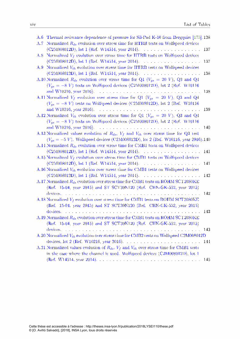
A.6 Thermal resistance dependence of pressure for Sil-Pad K-10 from Bergquist [175]. 128A.7 Normalized Rds evolution over stress time for HTRB tests on Wolfspeed devices
(C2M008012D), lot 1 (Ref. W14514, year 2014). . . . . . . . . . . . . . . . . . 137A.8 Normalized Vf evolution over stress time for HTRB tests on Wolfspeed devices
(C2M008012D), lot 1 (Ref. W14514, year 2014). . . . . . . . . . . . . . . . . . 137A.9 Normalized Vth evolution over stress time for HTRB tests on Wolfspeed devices
(C2M008012D), lot 1 (Ref. W14514, year 2014). . . . . . . . . . . . . . . . . . 138A.10 Normalized Rds evolution over stress time for Q1 (Vgs = 20 V ), Q3 and Q4
(Vgs = −8 V ) tests on Wolfspeed devices (C2M008012D), lot 2 (Ref. W10116and W10216, year 2016). . . . . . . . . . . . . . . . . . . . . . . . . . . . . . . 138
A.11 Normalized Vf evolution over stress time for Q1 (Vgs = 20 V ), Q3 and Q4(Vgs = −8 V ) tests on Wolfspeed devices (C2M008012D), lot 2 (Ref. W10116and W10216, year 2016). . . . . . . . . . . . . . . . . . . . . . . . . . . . . . . 139
A.12 Normalized Vth evolution over stress time for Q1 (Vgs = 20 V ), Q3 and Q4(Vgs = −8 V ) tests on Wolfspeed devices (C2M008012D), lot 2 (Ref. W10116and W10216, year 2016). . . . . . . . . . . . . . . . . . . . . . . . . . . . . . . 140
A.13 Normalized values evolution of Rds, Vf and Vth over stress time for Q3 test(Vgs = −5 V ). Wolfspeed devices (C2M008012D), lot 2 (Ref. W10116, year 2016).140
A.14 Normalized Rds evolution over stress time for CMB1 tests on Wolfspeed devices(C2M008012D), lot 1 (Ref. W14514, year 2014). . . . . . . . . . . . . . . . . . 141
A.15 Normalized Vf evolution over stress time for CMB1 tests on Wolfspeed devices(C2M008012D), lot 1 (Ref. W14514, year 2014). . . . . . . . . . . . . . . . . . 141
A.16 Normalized Vth evolution over stress time for CMB1 tests on Wolfspeed devices(C2M008012D), lot 1 (Ref. W14514, year 2014). . . . . . . . . . . . . . . . . . 142
A.17 NormalizedRds evolution over stress time for CMB1 tests on ROHM SCT2080KE(Ref. 15-04, year 2015) and ST SCT30N120 (Ref. CHN-GK-552, year 2015)devices. . . . . . . . . . . . . . . . . . . . . . . . . . . . . . . . . . . . . . . . . 142
A.18 Normalized Vf evolution over stress time for CMB1 tests on ROHM SCT2080KE(Ref. 15-04, year 2015) and ST SCT30N120 (Ref. CHN-GK-552, year 2015)devices. . . . . . . . . . . . . . . . . . . . . . . . . . . . . . . . . . . . . . . . . 143
A.19 NormalizedRds evolution over stress time for CMB1 tests on ROHM SCT2080KE(Ref. 15-04, year 2015) and ST SCT30N120 (Ref. CHN-GK-552, year 2015)devices. . . . . . . . . . . . . . . . . . . . . . . . . . . . . . . . . . . . . . . . . 143
A.20 Normalized Vth evolution over stress time for CMB2 tests onWolfspeed C2M008012Ddevices, lot 2 (Ref. W10216, year 2016). . . . . . . . . . . . . . . . . . . . . . . 144
A.21 Normalized values evolution of Rds, Vf and Vth over stress time for CMB1 testsin the case where the channel is used. Wolfspeed devices (C2M008012D), lot 1(Ref. W14514, year 2014). . . . . . . . . . . . . . . . . . . . . . . . . . . . . . . 145
Cette thèse est accessible à l'adresse : http://theses.insa-lyon.fr/publication/2018LYSEI110/these.pdf © [O. Aviñó Salvadó], [2018], INSA Lyon, tous droits réservés

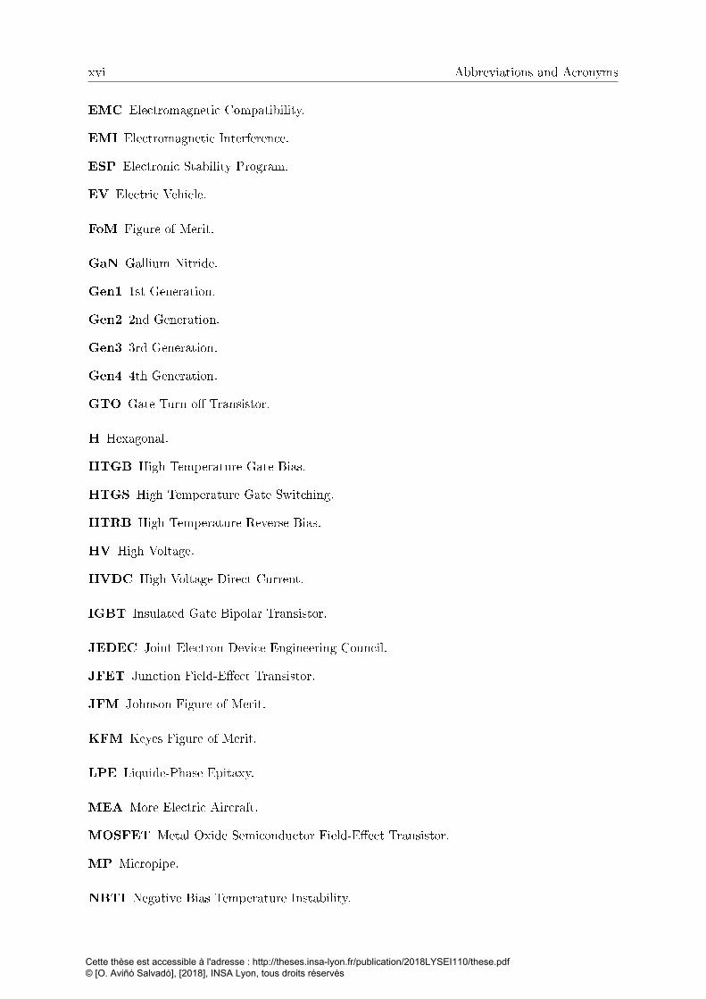
Abbreviations and Acronyms
3-C 3-C SiC polytype.
4-H 4-H SiC polytype.
6-H 6-H SiC polytype.
ABS Antilock Braking System.
AC Alternative Current.
BFM Baliga Figure of Merit.
BHFFM Baliga High Frequency Figure of Merit.
BJT Bipolar Junction Transistor.
BPD Basal Plane Dislocation.
BTI Bias Temperature Instability.
C Cubic.
CMB Chopper Mode Bias.
CVD Chemical Vapor Deposition.
DC Direct Current.
DLTS Deep Level Transient Spectroscopy.
DMOSFET Double-Implanted Metal Oxide Semiconductor Field-Eect Transistor.
DUT Device Under Test.
ED Edge Dislocation.
EHA Electro-Hydraulic Actuator.
EMA Electro-Mechanical Actuator.
Cette thèse est accessible à l'adresse : http://theses.insa-lyon.fr/publication/2018LYSEI110/these.pdf © [O. Aviñó Salvadó], [2018], INSA Lyon, tous droits réservés
xvi Abbreviations and Acronyms
EMC Electromagnetic Compatibility.
EMI Electromagnetic Interference.
ESP Electronic Stability Program.
EV Electric Vehicle.
FoM Figure of Merit.
GaN Gallium Nitride.
Gen1 1st Generation.
Gen2 2nd Generation.
Gen3 3rd Generation.
Gen4 4th Generation.
GTO Gate Turn-o Transistor.
H Hexagonal.
HTGB High Temperature Gate Bias.
HTGS High Temperature Gate Switching.
HTRB High Temperature Reverse Bias.
HV High Voltage.
HVDC High Voltage Direct Current.
IGBT Insulated Gate Bipolar Transistor.
JEDEC Joint Electron Device Engineering Council.
JFET Junction Field-Eect Transistor.
JFM Johnson Figure of Merit.
KFM Keyes Figure of Merit.
LPE Liquide-Phase Epitaxy.
MEA More Electric Aircraft.
MOSFET Metal Oxide Semiconductor Field-Eect Transistor.
MP Micropipe.
NBTI Negative Bias Temperature Instability.
Cette thèse est accessible à l'adresse : http://theses.insa-lyon.fr/publication/2018LYSEI110/these.pdf © [O. Aviñó Salvadó], [2018], INSA Lyon, tous droits réservés

Abbreviations and Acronyms xvii
PBTI Positive Bias Temperature Instability.
PCB Printed Circuit Board.
R Rhomboidal.
ROHM ROHM Semiconductorg.
SCR Silicon Controller Rectier.
SF Stacking Faults.
SiC Silicon Carbide.
SOFC Solid Oxide Fuel Cell.
ST STMicroelectronics.
TDDB Time Dependent Dielectric Breakdown.
TED Threading Edge Dislocation.
TRIAC Triode for Alternating Current.
TSD Threading Screw Dislocation.
TSP Thermo-sensitive Parameter.
U-MOSFET Trench gate MOSFET.
VD-MOSFET Vertical Diused MOSFET.
VJFET Vertical JFET.
VPE Vapour-Phase Epitaxy.
ZVS Zero Voltage Switching.
Cette thèse est accessible à l'adresse : http://theses.insa-lyon.fr/publication/2018LYSEI110/these.pdf © [O. Aviñó Salvadó], [2018], INSA Lyon, tous droits réservés

Cette thèse est accessible à l'adresse : http://theses.insa-lyon.fr/publication/2018LYSEI110/these.pdf © [O. Aviñó Salvadó], [2018], INSA Lyon, tous droits réservés

Acknowledgements
This work has been carried out at "Ampère Laboratory", in the Institut
National des Sciences Appliquées Lyon "INSA Lyon". It was funded as
part of the GENOME-PREMICES initiative, in the scope of the "Pro-
gramme d'Investissements d'Avenir" (Investments programm for the future)
of CORAC (French Research Council for Civil Aeronautics). My acknowl-
edgements to the public partner as well as to the industrial one, SAFRAN.
I would like to start giving thanks to the whole Ampere family, where
I arrived in '12 and which has given me the opportunity to work in many
projects. I am specially grateful for their welcome and because I have been
always very well treated.
I thank Dominique BERGOGNE for giving me the opportunity to came
at Ampère Laboratory; Guy CLERC, Christian MARTIN, Charles JOU-
BERT and Fabien SIXDENIER, who have trust in me to develop many
projects; Hervé MOREL and Cyril BUTTAY, who have addressed and
helped me during my PhD thesis in everything I have needed; as well as
Bruno ALLARD, director of the Ampère Laboratory, for their attention to
our needs.
I would also thank all the administrative and technical team for they
work, without which it would not been possible. A special recognition to
Pascal BEVILACQUA for his technical support and for his know-how.
My acknowledgements for all the members of the jury of my PhD thesis:
Nathalie MALBERT and Stéphane LEFEBVRE, for their interest in my
Phd thesis and to Alberto CASTELLAZZI and Francesco IANNUZZO for
their careful lecture and report of the manuscript. Of course, to my thesis
director and co-director, H. MOREL and C. BUTTAY for their accurate
Cette thèse est accessible à l'adresse : http://theses.insa-lyon.fr/publication/2018LYSEI110/these.pdf © [O. Aviñó Salvadó], [2018], INSA Lyon, tous droits réservés

xx Acknowledgements
corrections during the redaction phase.
Je voudrais aussi remercier les amis que je laisse ici, et que je compterevoir, ainsi que ceux qui sont partis avant moi. JB, Besar, Lu-Lu, Shiqin,Flo, Rémy C., Thilini, Hassan, Seyma, Mawad, Oualid et ceux qui pardon-neront mon oubli.
Également, je voudrais faire mention de ces MCF/Prof. qui m'ont tou-jours traité comme un égal, et à qui je vois plutôt comme des amis. Mercide votre accueil, ainsi que des soirées cohésion.
À H. Morel, dont j'apprécie beaucoup les qualités humaines et sa détermi-nation à se battre pour ce qu'il croit, dans tous les domaines. Un exemple.
À C. Buttay, qui a toujours été là pour moi de mon arrivée à Ampère.Pour son soutien, pour toujours trouver un moment.
À J. Papillon. Pour les bons moments passés pendant ces trois ans à lacoloc.
Donar les gràcies a la meva familia. Començant per la meva àvia, quevam perdre durant el meu segon any de tesis i que sempre va estar al meucostat. Com no, als meus pares i la meva germana, que sempre m'hananimat en aquest camí.
Finalment, agraïr a la meva parella, la Sandra, la paciència que hatingut durant aquets anys i l'ajuda que sempre m'ha prestat.
Thanks to everyone, I love you.
Merci à vous tous, je vous aime.
Gràcies a tots, us estimo.
Cette thèse est accessible à l'adresse : http://theses.insa-lyon.fr/publication/2018LYSEI110/these.pdf © [O. Aviñó Salvadó], [2018], INSA Lyon, tous droits réservés
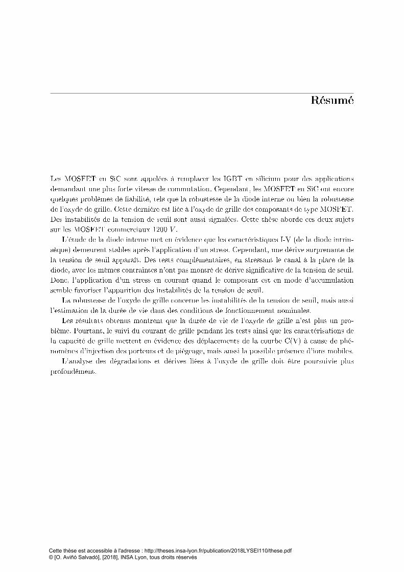
Résumé
Les MOSFET en SiC sont appelées à remplacer les IGBT en silicium pour des applicationsdemandant une plus forte vitesse de commutation. Cependant, les MOSFET en SiC ont encorequelques problèmes de abilité, tels que la robustesse de la diode interne ou bien la robustessede l'oxyde de grille. Cette dernière est liée à l'oxyde de grille des composants de type MOSFET.Des instabilités de la tension de seuil sont aussi signalées. Cette thèse aborde ces deux sujetssur les MOSFET commerciaux 1200 V .
L'étude de la diode interne met en évidence que les caractéristiques I-V (de la diode intrin-sèque) demeurent stables après l'application d'un stress. Cependant, une dérive surprenante dela tension de seuil apparaît. Des tests complémentaires, en stressant le canal à la place de ladiode, avec les mêmes contraintes n'ont pas montré de dérive signicative de la tension de seuil.Donc, l'application d'un stress en courant quand le composant est en mode d'accumulationsemble favoriser l'apparition des instabilités de la tension de seuil.
La robustesse de l'oxyde de grille concerne les instabilités de la tension de seuil, mais aussil'estimation de la durée de vie dans des conditions de fonctionnement nominales.
Les résultats obtenus montrent que la durée de vie de l'oxyde de grille n'est plus un pro-blème. Pourtant, le suivi du courant de grille pendant les tests ainsi que les caractérisations dela capacité de grille mettent en évidence des déplacements de la courbe C(V) à cause de phé-nomènes d'injection des porteurs et de piégeage, mais aussi la possible présence d'ions mobiles.
L'analyse des dégradations et dérives liées à l'oxyde de grille doit être poursuivie plusprofondément.
Cette thèse est accessible à l'adresse : http://theses.insa-lyon.fr/publication/2018LYSEI110/these.pdf © [O. Aviñó Salvadó], [2018], INSA Lyon, tous droits réservés

Cette thèse est accessible à l'adresse : http://theses.insa-lyon.fr/publication/2018LYSEI110/these.pdf © [O. Aviñó Salvadó], [2018], INSA Lyon, tous droits réservés
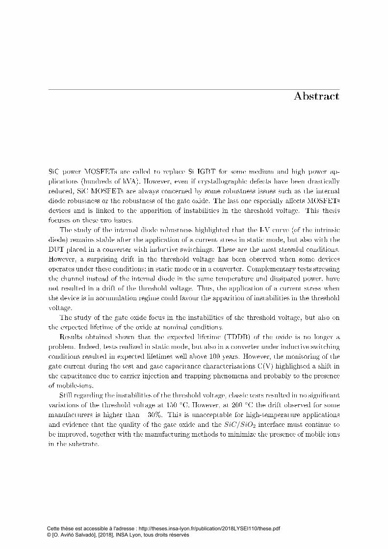
Abstract
SiC power MOSFETs are called to replace Si IGBT for some medium and high power ap-plications (hundreds of kVA). However, even if crystallographic defects have been drasticallyreduced, SiC MOSFETs are always concerned by some robustness issues such as the internaldiode robustness or the robustness of the gate oxide. The last one especially aects MOSFETsdevices and is linked to the apparition of instabilities in the threshold voltage. This thesisfocuses on these two issues.
The study of the internal diode robustness highlighted that the I-V curve (of the intrinsicdiode) remains stable after the application of a current stress in static mode, but also with theDUT placed in a converter with inductive switchings. These are the most stressful conditions.However, a surprising drift in the threshold voltage has been observed when some devicesoperates under these conditions; in static mode or in a converter. Complementary tests stressingthe channel instead of the internal diode in the same temperature and dissipated power, havenot resulted in a drift of the threshold voltage. Thus, the application of a current stress whenthe device is in accumulation regime could favour the apparition of instabilities in the thresholdvoltage.
The study of the gate oxide focus in the instabilities of the threshold voltage, but also onthe expected lifetime of the oxide at nominal conditions.
Results obtained shown that the expected lifetime (TDDB) of the oxide is no longer aproblem. Indeed, tests realized in static mode, but also in a converter under inductive switchingconditions resulted in expected lifetimes well above 100 years. However, the monitoring of thegate current during the test and gate capacitance characterizations C(V) highlighted a shift inthe capacitance due to carrier injection and trapping phenomena and probably to the presenceof mobile-ions.
Still regarding the instabilities of the threshold voltage, classic tests resulted in no signicantvariations of the threshold voltage at 150 C. However, at 200 C the drift observed for somemanufacturers is higher than +30%. This is unacceptable for high-temperature applicationsand evidence that the quality of the gate oxide and the SiC/SiO2 interface must continue tobe improved, together with the manufacturing methods to minimize the presence of mobile ionsin the substrate.
Cette thèse est accessible à l'adresse : http://theses.insa-lyon.fr/publication/2018LYSEI110/these.pdf © [O. Aviñó Salvadó], [2018], INSA Lyon, tous droits réservés

Cette thèse est accessible à l'adresse : http://theses.insa-lyon.fr/publication/2018LYSEI110/these.pdf © [O. Aviñó Salvadó], [2018], INSA Lyon, tous droits réservés
General Introduction
Human societies and electricity have evolved together since the end of 19th century. Inventionssuch as the telephone by Graham Bell in 1876, the lamp bulb by Joseph Wilson Swan in 1878[1] or the work of Nikola Tesla on electric machines provoked a real change on the live of theircontemporaries. Since then, electricity usage has not ceased to increase as more powerful andcomplex devices and machines have been introduced.
In this way, power electronics appeared at the beginning of the 20th century. Power elec-tronics is charged to adapt an electrical input to the characteristics of an electrical receptorand to control its parameters using power electronic devices.
The rst power electronic device was the mercury-arc valve (1902), invented by Peter CooperHewitt. After this, devices such as the ignitron, the phanotron, the thyratron and especiallythe vacuum valve dominated power electronics until the 50's [3].
In 1947 the rst Germanium transistor was invented by Bell Telephone Laboratories [4].This discovery would change electronics forever. In 1956 the rst thyristor or SCR (siliconcontrolled rectier) was developed, also by Bell Laboratories. This device was used exclu-sively in power electronics applications. After that, other power devices such as the GTO, the
Hydro OtherNuclearFossilTthermal
0
4T000
8T000
12T000
16T000
20T000
24T000
28T000
1971 1975 1980 1985 1990 1995 2000 2005 2010 2014
Year
Ele
ctri
cTP
ower
T(T
Wh)
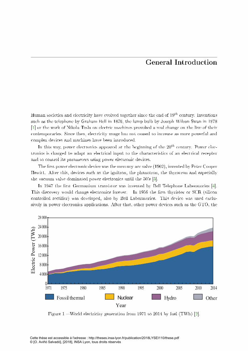
Figure 1 World electricity generation from 1971 to 2014 by fuel (TWh) [2].
Cette thèse est accessible à l'adresse : http://theses.insa-lyon.fr/publication/2018LYSEI110/these.pdf © [O. Aviñó Salvadó], [2018], INSA Lyon, tous droits réservés
2 General Introduction
Non-energy use16.2% Industry
8.0%
Transport64.5%
Other11.3%
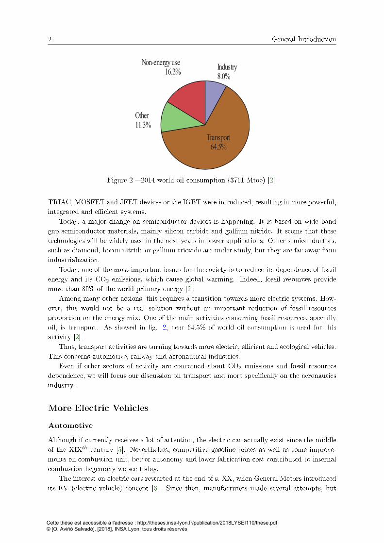
Figure 2 2014 world oil consumption (3761 Mtoe) [2].
TRIAC, MOSFET and JFET devices or the IGBT were introduced, resulting in more powerful,integrated and ecient systems.
Today, a major change on semiconductor devices is happening. It is based on wide bandgap semiconductor materials, mainly silicon carbide and gallium nitride. It seems that thesetechnologies will be widely used in the next years in power applications. Other semiconductors,such as diamond, boron nitride or gallium trioxide are under study, but they are far away fromindustrialization.
Today, one of the most important issues for the society is to reduce its dependence of fossilenergy and its CO2 emissions, which cause global warming. Indeed, fossil resources providemore than 80% of the world primary energy [2].
Among many other actions, this requires a transition towards more electric systems. How-ever, this would not be a real solution without an important reduction of fossil resourcesproportion on the energy mix. One of the main activities consuming fossil resources, speciallyoil, is transport. As showed in g. 2, near 64.5% of world oil consumption is used for thisactivity [2].
Thus, transport activities are turning towards more electric, ecient and ecological vehicles.This concerns automotive, railway and aeronautical industries.
Even if other sectors of activity are concerned about CO2 emissions and fossil resourcesdependence, we will focus our discussion on transport and more specically on the aeronauticsindustry.
More Electric Vehicles
Automotive
Although if currently receives a lot of attention, the electric car actually exist since the middleof the XIXth century [5]. Nevertheless, competitive gasoline prices as well as some improve-ments on combustion unit, better autonomy and lower fabrication cost contributed to internalcombustion hegemony we see today.
The interest on electric cars restarted at the end of s. XX, when General Motors introducedits EV (electric vehicle) concept [6]. Since then, manufacturers made several attempts, but
Cette thèse est accessible à l'adresse : http://theses.insa-lyon.fr/publication/2018LYSEI110/these.pdf © [O. Aviñó Salvadó], [2018], INSA Lyon, tous droits réservés
General Introduction 3
Motor BatteryDC/ACinverter
DC/DCboostconverter
DC/DCbuckconverter
AC/DCcharger
14V
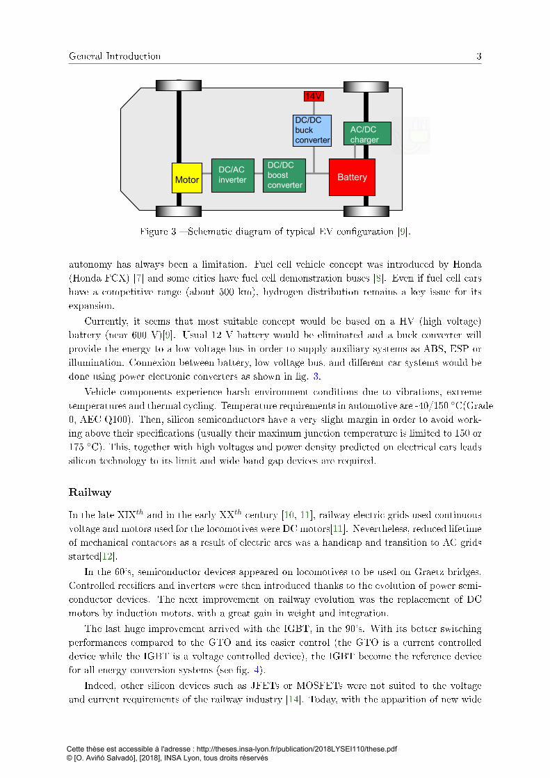
Figure 3 Schematic diagram of typical EV conguration [9].
autonomy has always been a limitation. Fuel cell vehicle concept was introduced by Honda(Honda FCX) [7] and some cities have fuel cell demonstration buses [8]. Even if fuel cell carshave a competitive range (about 500 km), hydrogen distribution remains a key issue for itsexpansion.
Currently, it seems that most suitable concept would be based on a HV (high voltage)battery (near 600 V)[9]. Usual 12 V battery would be eliminated and a buck converter willprovide the energy to a low voltage bus in order to supply auxiliary systems as ABS, ESP orillumination. Connexion between battery, low voltage bus, and dierent car systems would bedone using power electronic converters as shown in g. 3.
Vehicle components experience harsh environment conditions due to vibrations, extremetemperatures and thermal cycling. Temperature requirements in automotive are -40/150 C(Grade0, AEC Q100). Then, silicon semiconductors have a very slight margin in order to avoid work-ing above their specications (usually their maximum junction temperature is limited to 150 or175 C). This, together with high voltages and power density predicted on electrical cars leadssilicon technology to its limit and wide band gap devices are required.
Railway
In the late XIXth and in the early XXth century [10, 11], railway electric grids used continuousvoltage and motors used for the locomotives were DC motors[11]. Nevertheless, reduced lifetimeof mechanical contactors as a result of electric arcs was a handicap and transition to AC gridsstarted[12].
In the 60's, semiconductor devices appeared on locomotives to be used on Graetz bridges.Controlled rectiers and inverters were then introduced thanks to the evolution of power semi-conductor devices. The next improvement on railway evolution was the replacement of DCmotors by induction motors, with a great gain in weight and integration.
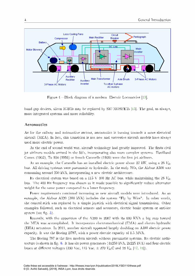
The last huge improvement arrived with the IGBT, in the 90's. With its better switchingperformances compared to the GTO and its easier control (the GTO is a current controlleddevice while the IGBT is a voltage controlled device), the IGBT become the reference devicefor all energy conversion systems (see g. 4).
Indeed, other silicon devices such as JFETs or MOSFETs were not suited to the voltageand current requirements of the railway industry [14]. Today, with the apparition of new wide
Cette thèse est accessible à l'adresse : http://theses.insa-lyon.fr/publication/2018LYSEI110/these.pdf © [O. Aviñó Salvadó], [2018], INSA Lyon, tous droits réservés
4 General Introduction
Figure 4 Block diagram of a modern Electric Locomotive [13].
band gap devices, siicon IGBTs may be replaced by SiC MOSFETs [15]. The goal, as always,more integrated systems and more reliability.
Aeronautics
As for the railway and automotive sectors, aeronautics is turning towards a more electricalaircraft (MEA). In fact, this transition is not new and successive aircraft models have alwaysused more electric power.
At the end of second world war, aircraft technology had greatly improved. The rsts civiljet airliners models arrived in the 50's, incorporating also more complex systems. HavillandComet (1952), Tu-104 (1956) or french Caravelle (1959) were the rst jet airliners.
As an example, the Caravelle has an installed electric power about 27 kW, using a 28 Vdcbus. All driving systems were pneumatic or hydraulic. In the early 70's, the Airbus A300 wasconsuming around 250 kVA, incorporating a new electric architecture.
Its electrical system was based on a 115 V 400 Hz AC bus, while maintaining the 28 Vdcbus. The 400 Hz frequency was chosen as it made possible to signicantly reduce alternatorweight for the same power compared to a lower frequency.
Power requirements continued increasing as new aircraft models were introduced. As anexample, the Airbus A320 (300 kVA) includes the system "Fly by Wire". In other words,the control stick was replaced by a simple joystick with electrical signal transmission. Otherexamples followed, such as electrical sensors and actuators, electric brake system or anti-icesystem (see g. 5).
Recently, with the apparition of the A380 in 2007 with its 600 KVA a big step towardthe MEA was accomplished. It incorporates electromechanical (EMA) and electro-hydraulic(EHA) actuators. In 2011, another aircraft appeared largely doubling on A380 electric powercapacity. It was the Boeing B787, with a power electric capacity of 1.5 MVA.
The Boeing 787 is the rst modern aircraft without pneumatic systems. Its electric archi-tecture is shown in g. 6. It has six power generators (4x250 kVA, 2x225 kVA) and four electricbuses at dierent voltages (230 Vac, 115 Vac, ± 270 VdcC and 28 Vdc [17, 18]).
Cette thèse est accessible à l'adresse : http://theses.insa-lyon.fr/publication/2018LYSEI110/these.pdf © [O. Aviñó Salvadó], [2018], INSA Lyon, tous droits réservés

General Introduction 5
Figure 5 Evolution of aircraft systems towards MEA [16].
S/G6C S/G5C
S/G1C
ElectricalCPowerCDistributionCSystemC
S/G4C S/G3C S/G2C
230CVACC3 PhaseC
VFC
230CVACC3 PhaseC
VFC
230CVACC3 PhaseC
VFC
250kVAC 250kVAC 250kVAC 250kVA
225kVAC 225kVAC
230CVACC3 PhaseCLoads
115CCCVACC3 PhaseCLoads
28CCCVDCCLoadsC
+/-270CVDCCLoadsC
Figure 6 Electrical structure on Boing 787 [17, 18].
The MEA concept is still in progress, with the development of reliable and ecient electricsystems. In this particular, wide band gap devices should allow to operate at higher voltagesand temperatures enabling further weight reduction. As in the Boeing 787, it is expected thatnew models will incorporate a HVDC bus 540 V (± 270 Vdc) [19]. Using higher voltages, wiresections can be reduced. Also, cooling systems size and weight could be reduced by usingdevices which can operate at higher temperatures.
One of the most promising wide band gap materials is SiC. As it will be detailed further inchapter 1, MOSFET structure has become the main SiC device for power applications because
Cette thèse est accessible à l'adresse : http://theses.insa-lyon.fr/publication/2018LYSEI110/these.pdf © [O. Aviñó Salvadó], [2018], INSA Lyon, tous droits réservés

6 General Introduction
it is a voltage controlled and normally-o device. Among the benets of SiC devices, thereis a drastic loses reduction thanks to SiC lower resistivity, but also due to their capability toswitch faster than silicon devices, minimizing commutation times. Moreover, they can drivemuch higher voltages than silicon devices for a given temperature and even it is envisaged touse SiC devices for high-temperature applications (>200 C).
This PhD thesis is involved in the project GENOME-PREMICES, which focuses in the MEAconcept. In the rst chapter we describe the state of the art on SiC semiconductor properties,power electronics semiconductor devices and their reliability. In a second time, chapters 2 and3 analyses two of the main reliability issues in SiC MOSFETs which limits their utilisation inaeronautics applications; the intrinsic diode and the gate dielectric robustness.
Cette thèse est accessible à l'adresse : http://theses.insa-lyon.fr/publication/2018LYSEI110/these.pdf © [O. Aviñó Salvadó], [2018], INSA Lyon, tous droits réservés
Chapter 1
State of the art in SiC devices
Contents
1.1 SiC semiconductor properties . . . . . . . . . . . . . . . . . . . 7
1.1.1 SiC Crystal Structure . . . . . . . . . . . . . . . . . . . . . . . . . . 8
1.1.2 Electric Properties . . . . . . . . . . . . . . . . . . . . . . . . . . . . 9
1.1.3 Comparative Properties . . . . . . . . . . . . . . . . . . . . . . . . . 19
1.2 Impact of crystallographic defects in SiC . . . . . . . . . 21
1.2.1 Main SiC crystallographic defects . . . . . . . . . . . . . . . . . . . . 21
1.2.2 SiC defects summary . . . . . . . . . . . . . . . . . . . . . . . . . . . 25
1.3 SiC Power Electronic Switches . . . . . . . . . . . . . . . . . 26
1.3.1 BJT . . . . . . . . . . . . . . . . . . . . . . . . . . . . . . . . . . . . 27
1.3.2 JFET . . . . . . . . . . . . . . . . . . . . . . . . . . . . . . . . . . . 28
1.3.3 MOSFET . . . . . . . . . . . . . . . . . . . . . . . . . . . . . . . . . 29
1.3.4 IGBT . . . . . . . . . . . . . . . . . . . . . . . . . . . . . . . . . . . 31
1.3.5 Comparison of SiC devices . . . . . . . . . . . . . . . . . . . . . . . . 33
1.4 SiC MOSFET robustness issues . . . . . . . . . . . . . . . . . . 34
1.4.1 Gate robustness . . . . . . . . . . . . . . . . . . . . . . . . . . . . . . 34
1.4.2 Internal diode robustness . . . . . . . . . . . . . . . . . . . . . . . . 40
1.4.3 Robustness under avalanche breakdown phenomenon . . . . . . . . . 42
1.4.4 Robustness under short-circuit conditions . . . . . . . . . . . . . . . 46
1.5 Conclusions . . . . . . . . . . . . . . . . . . . . . . . . . . . . . . . . . 50
1.1 SiC semiconductor properties
Since the apparition of the rst commercial silicon devices (grown junction) in 1954 [20], silicontechnology has become hegemonic. Indeed, silicon proprieties allow to be used over a wideapplications range. With a bandgap energy of 1.1 eV [21], manufactured silicon devices canreach temperatures near 200 C at 1000 V [22].
Nevertheless, the critical junction temperature follows an inverse relation with the break-down voltage. Then, developing devices for high temperature (>200 C) and high voltage(>600 V), silicon material is the principal limiting factor.
A wide type of applications, specially harsh environment applications, are requiring morepowerful systems and more performant semiconductor devices. As a result, the semiconductorindustry is turning towards wide band gap materials. Among these materials, SiC and GaNseems to be the most interesting in the short-term. Indeed other semiconductor materials, suchas diamond, are a long way from maturity.
Cette thèse est accessible à l'adresse : http://theses.insa-lyon.fr/publication/2018LYSEI110/these.pdf © [O. Aviñó Salvadó], [2018], INSA Lyon, tous droits réservés
8 1. State of the art in SiC devices
In this thesis, we will focus on SiC. GaN is a promising semiconductor material, but forhigh power applications, SiC is more interesting for the following reasons:
It is a massif material, thus it will allow to develop vertical devices. This will result inhigher voltage devices (>1200 V ). Today GaN devices are limited to 650 V .
SiC technology is more mature than GaN technology. First SiC commercial devicesappeared in early 2000's.
There are many elementary reliability issues which must to be solved in GaN until to beintroduced on industrial applications.
1.1.1 SiC Crystal Structure
SiC was discovered accidentally by J. Berzelius [23] in 1824, but industrial fabrication processwas not achieved until 1891 by E.G. Acheson [24]. In the rst half of the 20th century, SiCwas only considered for its mechanical and chemical properties [25].
In 1955, a patent from J.A. Lely [26] concerning SiC mono-crystal manufacturing by subli-mation opens the door to the rst semiconductor devices based on SiC substrates [27, 28, 29,30]. Silicon and Carbon, both elements of IV group of the periodic table of elements, formcovalent bonds [31] resulting in tetrahedral structures as shown in g. 1.1.
The actual crystal structure can dier in function of the tetrahedral stacking sequence,which can be symmetric or asymmetric. As a result, more than 200 types of crystal structures,called polytypes, have been mentioned in the literature [33]. Among them, there are the mainstructures used in electronics, which are listed in table 1.1 using Ramsdell notation [34] andrepresented in g. 1.2. In Ramsdell notation, the letter indicates the crystal structure of thepolytype (cubic, hexagonal or rhomboidal) and the number indicates the number of bilayers onthe stack sequence.
6-H was used rst for power electronics [36]. Even if its fabrication processus is morecomplicated, 4-H has replaced it, as it presents better electrical characteristics. The 3-C cubicstructure was used for photonics applications in the past, but it has been remplaced by GaNwhich shows brighter emission [37] due to GaN direct bandgap insted of the indirect one ofSiC. However, 3-C is still investigated for several applications, such as biosensors [38].
Carbon
Silicon
Carbon
Figure 1.1 SiC base tetrahedron. A carbon atom is bounded to four silicon atoms [32].
Cette thèse est accessible à l'adresse : http://theses.insa-lyon.fr/publication/2018LYSEI110/these.pdf © [O. Aviñó Salvadó], [2018], INSA Lyon, tous droits réservés

1.1. SiC semiconductor properties 9
Ramsdell Notation Structure SequenceSiC-3C Cubic ABCSiC-4H Hexagonal ABCBSiC-6H Hexagonal ABCACB
Table 1.1 Notation of most common SiC polytypes used in electronics [35].
BCBABCBA
BCACBABCACBA
4 H
CBACBA
3 C6 H
Figure 1.2 Cristalline structure of polytypes 4-H, 6-H and 3-C [35].
1.1.2 Electric Properties
The dierent nomenclatures used in this section are summarized in table 1.2.
1.1.2.1 Intrinsic Carrier Concentration ni
The intrinsic carrier concentration is determined by the quantity of electrons and holes thatparticipate in conduction [21]. Its concentration depends on temperature (T), bandgap energyof the material (EG) and the density of states in the valence band (NV ) and in the conductionband (NC) as specied by eq. (1.1).
ni =√NC ·NV · eEG/2kT (1.1)
where k is the Boltzmann's constant (1.38 · 10−23J/K) and T is the absolute temperature (K).The intrinsic carrier concentration of silicon and silicon carbide (4H) are given by eq. (1.2) and(1.3) respectively [21]. These equations are plotted in g. 1.3.
ni = 3.87 · 1016 · T 3/2 · e−7.02·103/T[cm−3
](1.2)
ni = 1.70 · 1016 · T 3/2 · e−2.08·104/T[cm−3
](1.3)
Cette thèse est accessible à l'adresse : http://theses.insa-lyon.fr/publication/2018LYSEI110/these.pdf © [O. Aviñó Salvadó], [2018], INSA Lyon, tous droits réservés

10 1. State of the art in SiC devices
Nomenclature Parameter Unitsα Impact ionization coecient cm−1
αn Impact ionization coecient for electrons cm−1
αp Impact ionization coecient for holes cm−1
µ Carrier mobility cm2 · V −1 · s−1
µ0 Electron mobility at low electric elds cm2 · V −1 · s−1
µn Electron mobility cm2 · V −1 · s−1
µp Holes mobility cm2 · V −1 · s−1
ρ Intrinsic resistivity cm · ΩεS Semiconductor dielectric constant -E Electric eld V · cm−1
Ec Critical electric eld V · cm−1
EG Bandgap energy eV
k Boltzmann's constant J/K
N Doping concentration cm−3
NA Acceptor concentration cm−3
NC Density of states in the conduction band cm−3
ND Donor concentration cm−3
ni Intrinsic carrier concentration cm−3
NV Density of states in the valence band cm−3
Q Electric charge C
q Electron charge C
Ron,sp Specic on-resistance Ω · cm−3
T Temperature K
Vbi Built-in potential V
Vbr Breakdown voltage V
vsat Saturated drift velocity cm · s−1
Va Applied bias V
vD Carrier velocity cm · s−1
WD Depletion region width cm
Table 1.2 Table of symbols.
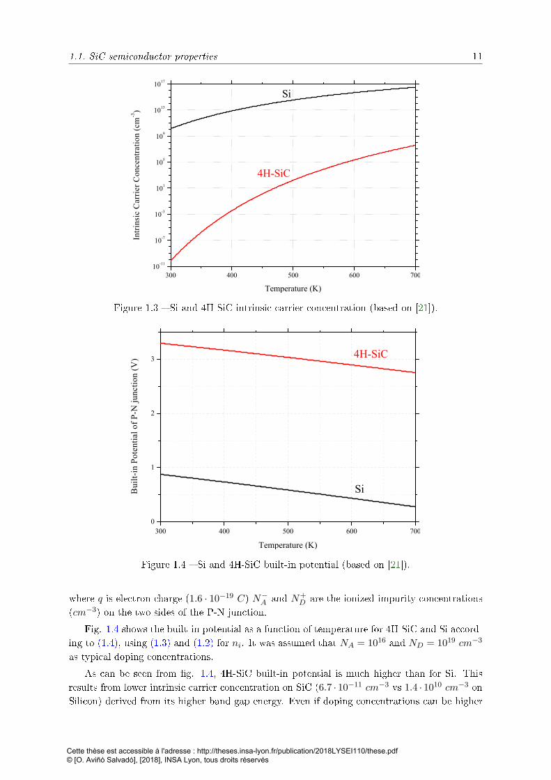
As shown in g. 1.3, ni increases with temperature, but remains much smaller for SiCthan that for Si, as a result of its larger energy bandgap. At 300 K, 4H-SiC intrinsic carrierconcentration is 6.7 · 10−11 cm−3, compared to 1.4 · 1010 cm−3 for Si. As a consequence, SiCdevices oer a lower leakage current (bulk generation current is negligible) and a capability tooperate at higher temperature.
1.1.2.2 Built-in Potential Vbi
The built-in potential (Vbi) in a semiconductor is dened as the potential across the depletionregion which occurs around an abrupt PN junction in thermal equilibrium and is given by eq.(1.4) [21].
Vbi =k · Tq· ln
(N−A ·N+
D
n2i
)(1.4)
Cette thèse est accessible à l'adresse : http://theses.insa-lyon.fr/publication/2018LYSEI110/these.pdf © [O. Aviñó Salvadó], [2018], INSA Lyon, tous droits réservés
1.1. SiC semiconductor properties 11
300 400 500 600 70010
-11
10-7
10-3
101
105
109
1013
1017
Intr
insi
c C
arri
er C
once
ntra
tion
(cm
-3)
Temperature (K)
Si
4H-SiC
Figure 1.3 Si and 4H-SiC intrinsic carrier concentration (based on [21]).
300 400 500 600 7000
1
2
3
SiBui
lt-i
nrP
oten
tial
rofr
P-N
rjunc
tion
r(V
)
Temperaturer(K)
4H-SiC
Figure 1.4 Si and 4H-SiC built-in potential (based on [21]).
where q is electron charge (1.6 · 10−19 C) N−A and N+D are the ionized impurity concentrations
(cm−3) on the two sides of the P-N junction.
Fig. 1.4 shows the built-in potential as a function of temperature for 4H-SiC and Si accord-ing to (1.4), using (1.3) and (1.2) for ni. It was assumed that NA = 1016 and ND = 1019 cm−3
as typical doping concentrations.
As can be seen from g. 1.4, 4H-SiC built-in potential is much higher than for Si. Thisresults from lower intrinsic carrier concentration on SiC (6.7 · 10−11 cm−3 vs 1.4 · 1010 cm−3 onSilicon) derived from its higher band gap energy. Even if doping concentrations can be higher
Cette thèse est accessible à l'adresse : http://theses.insa-lyon.fr/publication/2018LYSEI110/these.pdf © [O. Aviñó Salvadó], [2018], INSA Lyon, tous droits réservés
12 1. State of the art in SiC devices
300 350 400 450 5000
200
400
600
800
1000
1200
1400
4H-SiCeµn
Sieµp
Mob
ilit
ye(c
m2 /V
·s)
Temperaturee(K)
Sieµn
Figure 1.5 Si (electron and holes) and 4H-SiC (electron) mobility dependence on temperature(based on [21]).
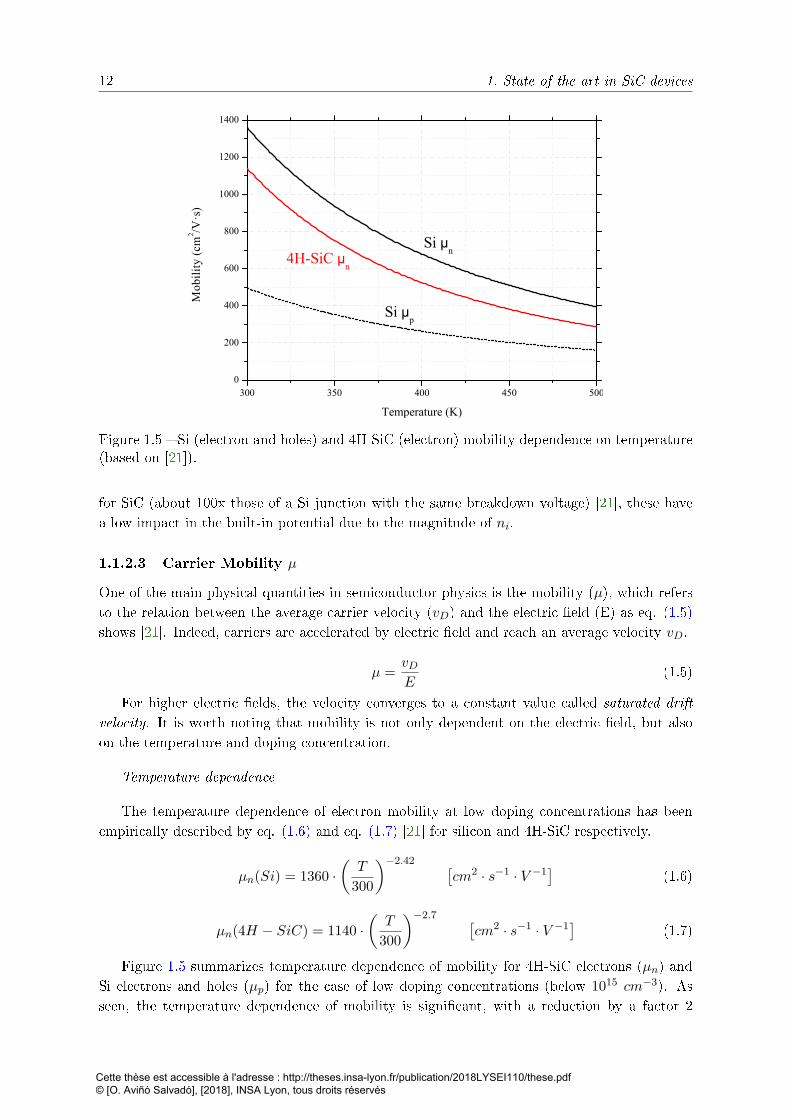
for SiC (about 100x those of a Si junction with the same breakdown voltage) [21], these havea low impact in the built-in potential due to the magnitude of ni.
1.1.2.3 Carrier Mobility µ
One of the main physical quantities in semiconductor physics is the mobility (µ), which refersto the relation between the average carrier velocity (vD) and the electric eld (E) as eq. (1.5)shows [21]. Indeed, carriers are accelerated by electric eld and reach an average velocity vD.
µ =vDE
(1.5)
For higher electric elds, the velocity converges to a constant value called saturated driftvelocity. It is worth noting that mobility is not only dependent on the electric eld, but alsoon the temperature and doping concentration.
Temperature dependence
The temperature dependence of electron mobility at low doping concentrations has beenempirically described by eq. (1.6) and eq. (1.7) [21] for silicon and 4H-SiC respectively.
µn(Si) = 1360 ·(T
300
)−2.42 [cm2 · s−1 · V −1
](1.6)
µn(4H − SiC) = 1140 ·(T
300
)−2.7 [cm2 · s−1 · V −1
](1.7)
Figure 1.5 summarizes temperature dependence of mobility for 4H-SiC electrons (µn) andSi electrons and holes (µp) for the case of low doping concentrations (below 1015 cm−3). Asseen, the temperature dependence of mobility is signicant, with a reduction by a factor 2
Cette thèse est accessible à l'adresse : http://theses.insa-lyon.fr/publication/2018LYSEI110/these.pdf © [O. Aviñó Salvadó], [2018], INSA Lyon, tous droits réservés
1.1. SiC semiconductor properties 13
1E14 1E15 1E16 1E17 1E18 1E190
200
400
600
800
1000
1200
1400
4H-SiC)µn
Si)µp
Si)µn
Mob
ilit
y)(c
m2
/)V·s
)
Doping)Concentration)(cm-3)
Figure 1.6 Si (electron and holes) and 4H-SiC (electron) mobility dependence of dopingconcentration (based on [21]).
between 300 and 400 K which is the usual temperature range of operation for power devices.The mobility plays a major role in the resistivity of the semiconductor material, as describedby eq. (1.8), where ρ is the resistivity and N is the doping concentration.
ρ =1
q · µ ·N (1.8)
Doping concentration dependence
At low doping concentrations (below 1016), mobility remains near constant and phononscattering is the principal limiting phenomenon. At higher doping concentrations Coulombicscattering becomes important, reducing mobility. This is due to ionized impurity scatteringwith ionized doping atoms [39]. This behaviour, was empirically modelled by eq. (1.9)[39].
µ = µmin +µmax − µmin1 +
(N
Nr
)α (1.9)
where N is the donor/acceptor concentration, µmin and µmax are the minimal and maximalmobility. Nr and α are tting parameters. For 4H-SiC the eq. becomes [21]:
µn(4H − SiC) =4.05 · 1013 + 20N0.61
D
3.55 · 1010 +N0.61D
[cm2 · s−1 · V −1
](1.10)
Electric eld dependence
Electron and holes mobility in silicon is considered independent from the electric eld below103 V · cm−1. For higher electric elds, carrier velocity increases sub-linearly until it reachesthe saturated drift velocity which is also temperature-dependent.
Cette thèse est accessible à l'adresse : http://theses.insa-lyon.fr/publication/2018LYSEI110/these.pdf © [O. Aviñó Salvadó], [2018], INSA Lyon, tous droits réservés
14 1. State of the art in SiC devices
102
103
104
105
106
101
102
103
104
Mob
ilit
y (c
m2
/ V·s
)
Electric Field (V/cm)
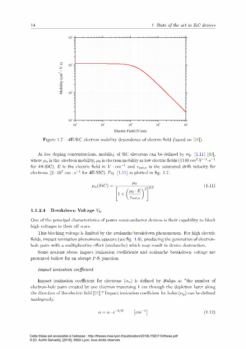
Figure 1.7 4H-SiC electron mobility dependence of electric eld (based on [21]).
At low doping concentrations, mobility of SiC electrons can be dened by eq. (1.11) [40],where µn is the electron mobility, µ0 is electron mobility at low electric elds (1140 cm2·V −1·s−1
for 4H-SiC), E is the electric eld in V · cm−1 and vsat,n is the saturated drift velocity forelectrons (2 · 107 cm · s−1 for 4H-SIC). Eq. (1.11) is plotted in g. 1.7.
µn(SiC) =µ0[
1 +
(µ0 · Evsat,n
)2]0.5 (1.11)
1.1.2.4 Breakdown Voltage Vbr
One of the principal characteristics of power semiconductor devices is their capability to blockhigh voltages in their o state.
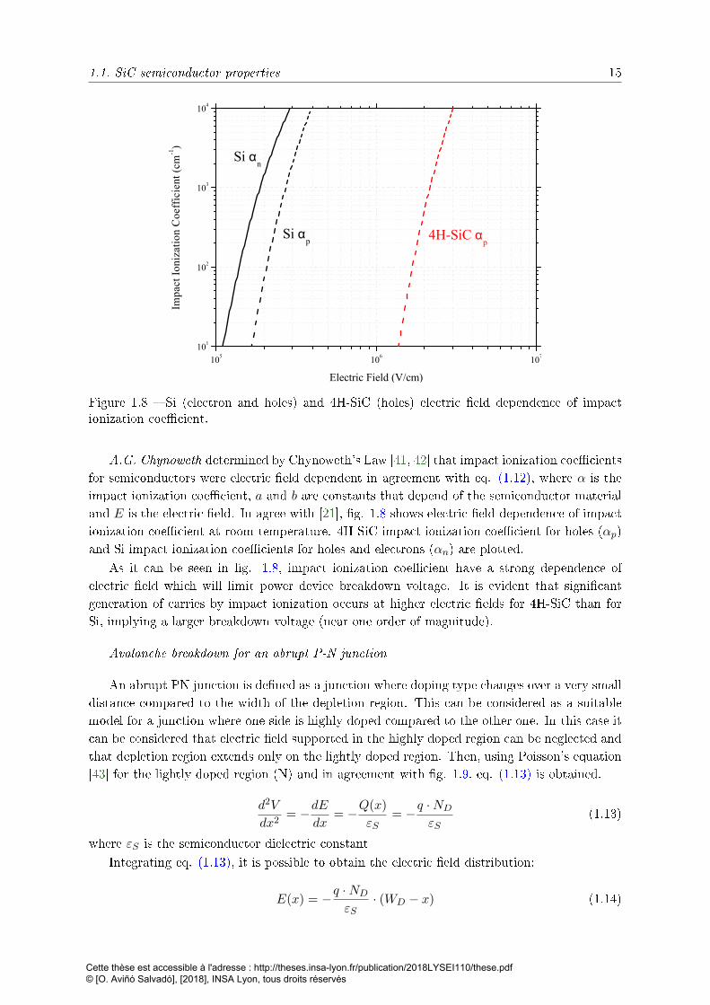
This blocking voltage is limited by the avalanche breakdown phenomenon. For high electricelds, impact ionization phenomena appears (see g. 1.8), producing the generation of electron-hole pairs with a multiplicative eect (avalanche) which may result in device destruction.
Some notions about impact ionization coecients and avalanche breakdown voltage arepresented bellow for an abrupt P-N junction.
Impact ionization coecient
Impact ionization coecient for electrons (αn) is dened by Baliga as "the number ofelectron-hole pairs created by one electron traversing 1 cm through the depletion layer alongthe direction of the electric eld [21]." Impact ionization coecient for holes (αp) can be denedanalogously.
α = a · e−b/E[cm−1
](1.12)
Cette thèse est accessible à l'adresse : http://theses.insa-lyon.fr/publication/2018LYSEI110/these.pdf © [O. Aviñó Salvadó], [2018], INSA Lyon, tous droits réservés
1.1. SiC semiconductor properties 15
105
106
107
101
102
103
104
4H-SiCdαp
Impa
ctdI
oniz
atio
ndC
oeff
icie
ntd(
cm-1
)
ElectricdFieldd(V/cm)
Sidαn
Sidαp
Figure 1.8 Si (electron and holes) and 4H-SiC (holes) electric eld dependence of impactionization coecient.
A.G. Chynoweth determined by Chynoweth's Law [41, 42] that impact ionization coecientsfor semiconductors were electric eld dependent in agreement with eq. (1.12), where α is theimpact ionization coecient, a and b are constants that depend of the semiconductor materialand E is the electric eld. In agree with [21], g. 1.8 shows electric eld dependence of impactionization coecient at room temperature. 4H-SiC impact ionization coecient for holes (αp)and Si impact ionization coecients for holes and electrons (αn) are plotted.
As it can be seen in g. 1.8, impact ionization coecient have a strong dependence ofelectric eld which will limit power device breakdown voltage. It is evident that signicantgeneration of carries by impact ionization occurs at higher electric elds for 4H-SiC than forSi, implying a larger breakdown voltage (near one order of magnitude).
Avalanche breakdown for an abrupt P-N junction
An abrupt PN junction is dened as a junction where doping type changes over a very smalldistance compared to the width of the depletion region. This can be considered as a suitablemodel for a junction where one side is highly doped compared to the other one. In this case itcan be considered that electric eld supported in the highly doped region can be neglected andthat depletion region extends only on the lightly doped region. Then, using Poisson's equation[43] for the lightly doped region (N) and in agreement with g. 1.9, eq. (1.13) is obtained.
d2V
dx2= −dE
dx= −Q(x)
εS= −q ·ND
εS(1.13)
where εS is the semiconductor dielectric constant
Integrating eq. (1.13), it is possible to obtain the electric eld distribution:
E(x) = −q ·ND
εS· (WD − x) (1.14)
Cette thèse est accessible à l'adresse : http://theses.insa-lyon.fr/publication/2018LYSEI110/these.pdf © [O. Aviñó Salvadó], [2018], INSA Lyon, tous droits réservés

16 1. State of the art in SiC devices
Figure 1.9 Electric eld and potential distribution for an abrupt parallel-plane P+-N junction[21].
Integrating eq. (1.14) and assuming that electric eld is zero at the end of the depletionregion (x = WD), yields the electric potential distribution:
V (x) =q ·ND
εS· (WD · x−
x2
2) (1.15)
The maximal value of the electric eld and potential are expressed by eq. (1.16) and eq.(1.17) respectively.
E(x)max =q ·ND ·WD
εS(1.16)
V (x)max =q ·ND ·W 2
D
2 · εS(1.17)
Considering an applied bias Va as the maximal potential, it is possible to rewrite eq. (1.17)to obtain the thickness of the depletion region:
WD =
√2 · εS · Vaq ·ND
(1.18)
For 4H-SiC, Baliga [21] provides equations (1.19) and (1.20) expressing respectively thebreakdown voltage and the depletion region thickness as a function of the doping concentration.These are plotted in gures 1.10 and 1.11 and compared to Silicon. It is considered [21] thatbreakdown phenomena occurs when the integral of the impact ionization coecient on thedepletion region becomes equal to unity.
Vbr = 3.0 · 1015 ·N−3/4D [V ] (1.19)
WDmax = 1.82 · 1011 ·N−7/8D [cm] (1.20)
Cette thèse est accessible à l'adresse : http://theses.insa-lyon.fr/publication/2018LYSEI110/these.pdf © [O. Aviñó Salvadó], [2018], INSA Lyon, tous droits réservés
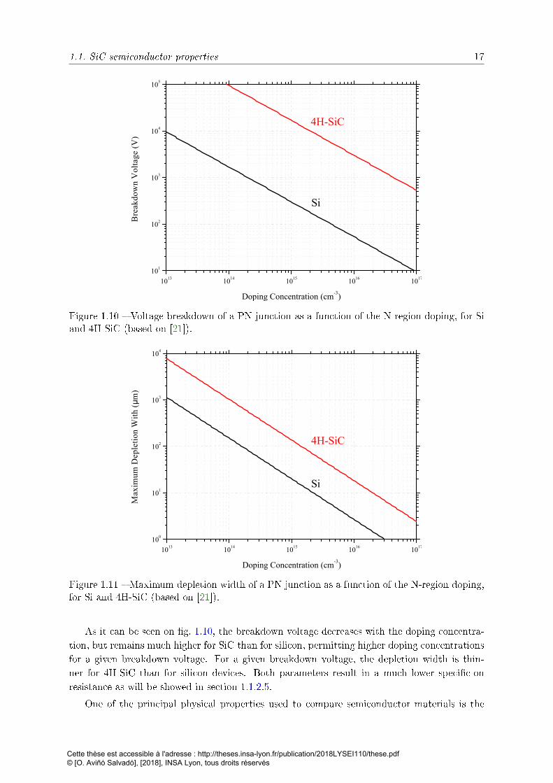
1.1. SiC semiconductor properties 17
1013
1014
1015
1016
1017
101
102
103
104
105
Si
4H-SiCB
reak
dow
ncV
olta
gec(
V)
DopingcConcentrationc(cm-3)
Figure 1.10 Voltage breakdown of a PN junction as a function of the N-region doping, for Siand 4H-SiC (based on [21]).
1013
1014
1015
1016
1017
100
101
102
103
104
Max
imum
SDep
leti
onSW
ithS
(µm
)
DopingSConcentrationS(cm-3
)
Si
4H-SiC
Figure 1.11 Maximum depletion width of a PN junction as a function of the N-region doping,for Si and 4H-SiC (based on [21]).
As it can be seen on g. 1.10, the breakdown voltage decreases with the doping concentra-tion, but remains much higher for SiC than for silicon, permitting higher doping concentrationsfor a given breakdown voltage. For a given breakdown voltage, the depletion width is thin-ner for 4H-SiC than for silicon devices. Both parameters result in a much lower specic-onresistance as will be showed in section 1.1.2.5.
One of the principal physical properties used to compare semiconductor materials is the
Cette thèse est accessible à l'adresse : http://theses.insa-lyon.fr/publication/2018LYSEI110/these.pdf © [O. Aviñó Salvadó], [2018], INSA Lyon, tous droits réservés
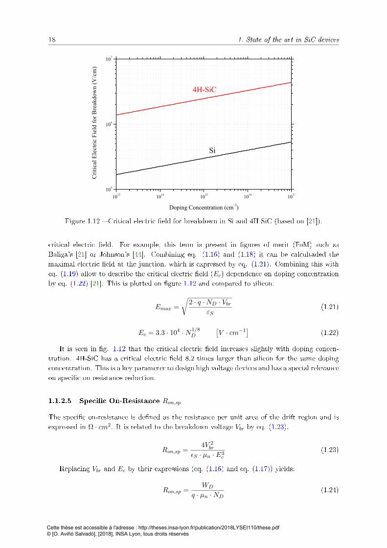
18 1. State of the art in SiC devices
1013
1014
1015
1016
1017
105
106
107
Cri
tica
lpEle
ctri
cpF
ield
pfor
pBre
akdo
wnp
(V/c
m)
DopingpConcentrationp(cm-3)
Si
4H-SiC
Figure 1.12 Critical electric eld for breakdown in Si and 4H-SiC (based on [21]).
critical electric eld. For example, this term is present in gures of merit (FoM) such asBaliga's [21] or Johnson's [44]. Combining eq. (1.16) and (1.18) it can be calcultaded themaximal electric eld at the junction, which is expressed by eq. (1.21). Combining this witheq. (1.19) allow to describe the critical electric eld (Ec) dependence on doping concentrationby eq. (1.22) [21]. This is plotted on gure 1.12 and compared to silicon.
Emax =
√2 · q ·ND · Vbr
εS(1.21)
Ec = 3.3 · 104 ·N1/8D
[V · cm−1
](1.22)
It is seen in g. 1.12 that the critical electric eld increases slightly with doping concen-tration. 4H-SiC has a critical electric eld 8.2 times larger than silicon for the same dopingconcentration. This is a key parameter to design high voltage devices and has a special relevanceon specic on-resistance reduction.
1.1.2.5 Specic On-Resistance Ron,sp
The specic on-resistance is dened as the resistance per unit area of the drift region and isexpressed in Ω · cm2. It is related to the breakdown voltage Vbr by eq. (1.23).
Ron,sp =4V 2
br
εS · µn · E3c
(1.23)
Replacing Vbr and Ec by their expressions (eq. (1.16) and eq. (1.17)) yields:
Ron,sp =WD
q · µn ·ND(1.24)
Cette thèse est accessible à l'adresse : http://theses.insa-lyon.fr/publication/2018LYSEI110/these.pdf © [O. Aviñó Salvadó], [2018], INSA Lyon, tous droits réservés
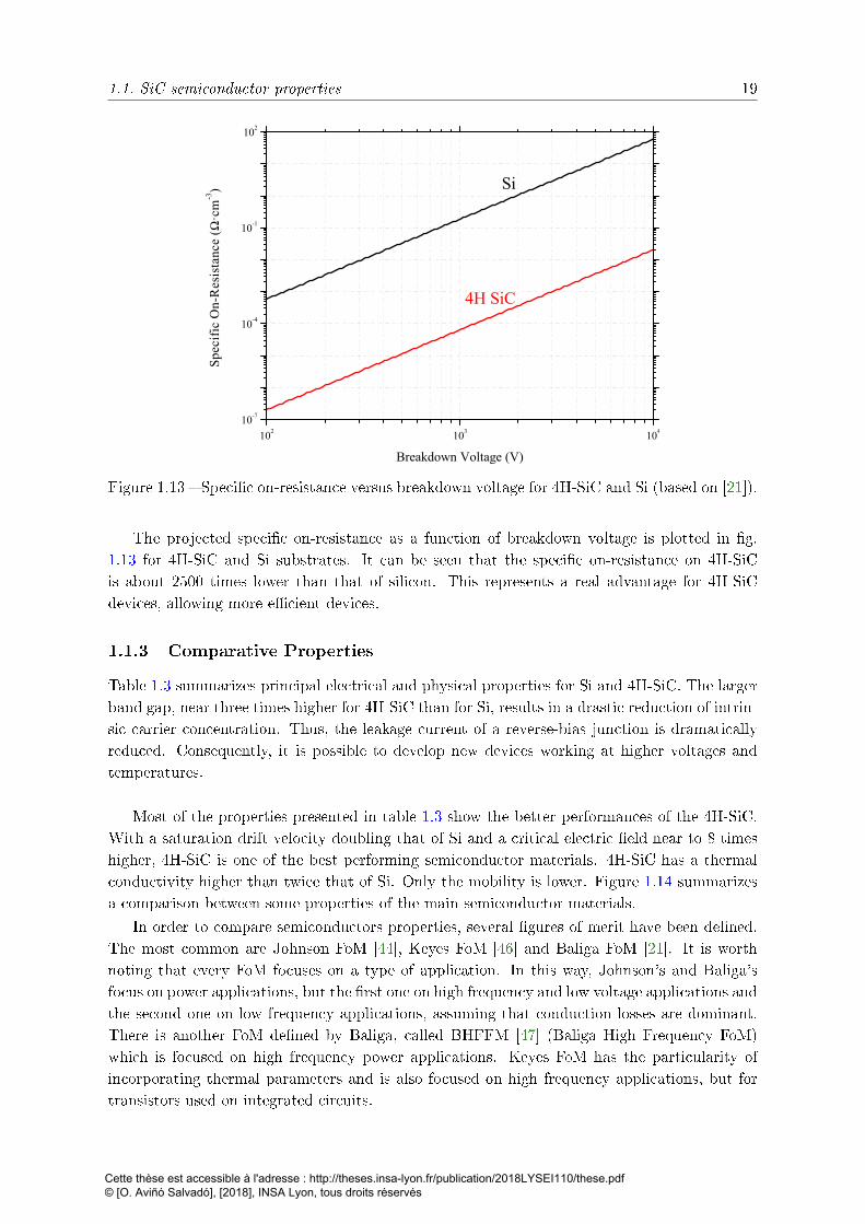
1.1. SiC semiconductor properties 19
102
103
104
10-7
10-4
10-1
102
Spe
cifi
clO
n-R
esis
tanc
el(Ω
·cm
-3)
BreakdownlVoltagel(V)
Si
4HlSiC
Figure 1.13 Specic on-resistance versus breakdown voltage for 4H-SiC and Si (based on [21]).
The projected specic on-resistance as a function of breakdown voltage is plotted in g.1.13 for 4H-SiC and Si substrates. It can be seen that the specic on-resistance on 4H-SiCis about 2500 times lower than that of silicon. This represents a real advantage for 4H-SiCdevices, allowing more ecient devices.
1.1.3 Comparative Properties
Table 1.3 summarizes principal electrical and physical properties for Si and 4H-SiC. The largerband gap, near three times higher for 4H-SiC than for Si, results in a drastic reduction of intrin-sic carrier concentration. Thus, the leakage current of a reverse-bias junction is dramaticallyreduced. Consequently, it is possible to develop new devices working at higher voltages andtemperatures.
Most of the properties presented in table 1.3 show the better performances of the 4H-SiC.With a saturation drift velocity doubling that of Si and a critical electric eld near to 8 timeshigher, 4H-SiC is one of the best performing semiconductor materials. 4H-SiC has a thermalconductivity higher than twice that of Si. Only the mobility is lower. Figure 1.14 summarizesa comparison between some properties of the main semiconductor materials.
In order to compare semiconductors properties, several gures of merit have been dened.The most common are Johnson FoM [44], Keyes FoM [46] and Baliga FoM [21]. It is worthnoting that every FoM focuses on a type of application. In this way, Johnson's and Baliga'sfocus on power applications, but the rst one on high frequency and low voltage applications andthe second one on low frequency applications, assuming that conduction losses are dominant.There is another FoM dened by Baliga, called BHFFM [47] (Baliga High Frequency FoM)which is focused on high frequency power applications. Keyes FoM has the particularity ofincorporating thermal parameters and is also focused on high frequency applications, but fortransistors used on integrated circuits.
Cette thèse est accessible à l'adresse : http://theses.insa-lyon.fr/publication/2018LYSEI110/these.pdf © [O. Aviñó Salvadó], [2018], INSA Lyon, tous droits réservés
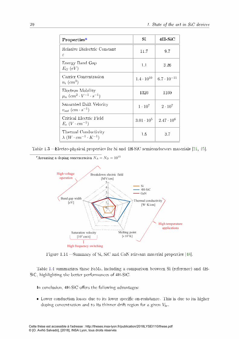
20 1. State of the art in SiC devices
Propertiesa Si 4H-SiC
Relative Dielectric Constantε
11.7 9.7
Energy Band GapEG (eV )
1.1 3.26
Carrier Concentrationni (cm3)
1.4 · 1010 6.7 · 10−11
Electron Mobilityµn (cm2 · V −1 · s−1)
1320 1100
Saturated Drift Velocityvsat (cm · s−1)
1 · 107 2 · 107
Critical Electric FieldEc (V · cm−1)
3.01 · 105 2.47 · 106
Thermal Conductivityλ (W · cm−1 ·K−1)
1.5 3.7
Table 1.3 Electro-physical properties for Si and 4H-SiC semiconductors materials [21, 45].
aAssuming a doping concentration NA = ND = 1015
Si4HqSiCGaN
5
4
3
2
1
0
Breakdownmelectric field[MV/cm]
Bandmgapmwidth[eV]
Saturationmvelocity[107 cm/s]
Melting point[x 103 K]
Thermalmconductivity[W·K/cm]
Highmfrequency switching
Highmvoltagemoperation
Highmtemperatureapplications
Figure 1.14 Summary of Si, SiC and GaN relevant material properties [48].
Table 1.4 summarizes these FoMs, including a comparison between Si (reference) and 4H-SiC, highlighting the better performances of 4H-SiC.
In conclusion, 4H-SiC oers the following advantages:
Lower conduction losses due to its lower specic on-resistance. This is due to its higherdoping concentration and to its thinner drift region for a given Vbr.
Cette thèse est accessible à l'adresse : http://theses.insa-lyon.fr/publication/2018LYSEI110/these.pdf © [O. Aviñó Salvadó], [2018], INSA Lyon, tous droits réservés
1.2. Impact of crystallographic defects in SiC 21
FoM Equation Si 4H-SiC
JohnsonJFM
E2c · v2
sat
4 · π21 410
KeyesKFMa
λ ·√c · vsat4π · ε 1 5.1
BaligaBFM
ε · µ · E3c 1 290
Baliga HFBHFFM b
µ · E2c
2·√VgV 3br
1 34
Table 1.4 FoM summary and comparative between 4H-SiC and Si [44, 21, 46, 47, 49, 45].
ac is light speed in vacuum.bVg is gate voltage.
Higher voltage devices can be designed thanks to the higher critical electric eld of 4H-SiC. Its lower carrier concentration minimizes leakage current in the o-state.
Its better thermal performances, could open the way towards high temperature and moreintegrated devices, particularly on devices without gate oxide.
1.2 Impact of crystallographic defects in SiC
Electronic devices manufacturing involves many steps which have to be realised carefully. Anydefect introduced during the dierent manufacturing phases or material nishing could resultin a failure of the device.
One of the critical process step is the growth of SiC on a SiC substrate (epitaxy).
The most common method to grow SiC crystal is VPE (Vapour-Phase Epitaxy). Thisprocess is capable to produce high quality material. In spite of the high crystal quality, im-provements are required in order to minimize material defects. In this way, dierent approacheson CVD (chemical vapor deposition) [50] have been presented, showing as micropipes defectswhere properly closed. Also, LPE (liquide-phase epitaxy) technique has been studied [51],repporting a defect number reduction.
Even if further description of epitaxy techniques are not the focus of this document, adescription of the principal material defects is necessary. This is described and summarizedbelow.
1.2.1 Main SiC crystallographic defects
The most important defect encountered in SiC crystals are micropipes. These are thermody-namically stable hollow core screw dislocations [52]. On a wafer, they consist on a hole about1 µm diameter in size [53]. Thus, a device with a micropipe defect is no longer capable tosupport a high electric eld. It is considered as a critical defect which manufacturing compa-nies try to eliminate. Commercial SiC wafers are usually classied by the rate of defects [54].
Cette thèse est accessible à l'adresse : http://theses.insa-lyon.fr/publication/2018LYSEI110/these.pdf © [O. Aviñó Salvadó], [2018], INSA Lyon, tous droits réservés

22 1. State of the art in SiC devices
Today, it is possible to produce 150 mm diameter 4H-SiC wafers without any micropipe defect[54].
Unfortunately, micropipes are not the only type of defect which can be found in SiC crystals.There are several other types of defects which can be classied in two sets:
SiC wafer defects.
Epitaxial defects.
A type of defect, called stacking fault (SF) could be classied in the wafer defect category.But, as it can propagate through the epitaxial layer and because it is of high importance onSiC devices, a special section is dedicated to it.
1.2.1.1 SiC wafer defects
The principal defects relative to wafer substrate are the following:
Basal plane dislocations (BPD).
Edge dislocations (ED).
Core screw dislocations.
Basal plane dislocations are planar defects of the crystal, which perturb its periodicity. Thistype of defect can spread to the substrate surface, where the epitaxy has to be realised. Then,this can result in a defect in the epitaxy layer. Due to its unstable nature, BPD can evolve toanother kind of defect called staking fault (SF) under conditions of bipolar injection [55]. As SFand BPD can be potentially critical, it is usual to use advanced epitaxial growth and engravingtechniques [56] to transform this type of defect into TED (Threading Edge Dislocation) defects,which are considered as not critical [53, 57].
Edge dislocations are usually one-dimension defects on the surface of the wafer that getannealed during the epitaxial growth [53]. An edge dislocation defect is caused by the absenceof an inter-atomic bonding. This kind of defect rarely aects devices operation.
Core screw dislocation is a type of defect similar to micropipes, which evolves over thethickness of the SiC wafer. This defect might continue over the epitaxy layer depending ofseveral factors such as epitaxial growth techniques. It is known that this kind of defect resultsin a lower critical electric eld [58] and lower carrier lifetime of the epitaxial layers grown overthem [53, 59]. Some studies show that is possible to properly close core screw dislocations,limiting the reduction of the critical electric eld to around 10% [60].
Finally, other defects such as low angle boundaries or defects due to polishing processes [53]are presents on commercial wafers and cause a leakage current augmentation when devices areunder reverse bias conditions.
Cette thèse est accessible à l'adresse : http://theses.insa-lyon.fr/publication/2018LYSEI110/these.pdf © [O. Aviñó Salvadó], [2018], INSA Lyon, tous droits réservés
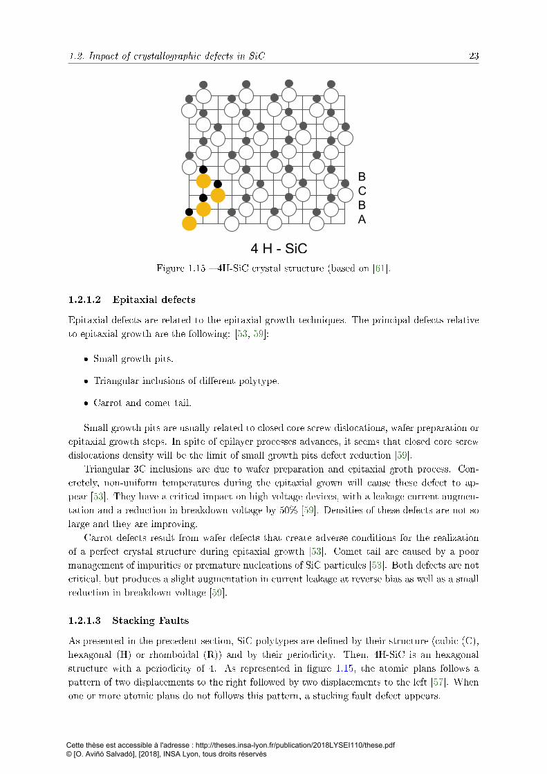
1.2. Impact of crystallographic defects in SiC 23
4 H - SiC
BCBA
Figure 1.15 4H-SiC crystal structure (based on [61].
1.2.1.2 Epitaxial defects
Epitaxial defects are related to the epitaxial growth techniques. The principal defects relativeto epitaxial growth are the following: [53, 59]:
Small growth pits.
Triangular inclusions of dierent polytype.
Carrot and comet tail.
Small growth pits are usually related to closed core screw dislocations, wafer preparation orepitaxial growth steps. In spite of epilayer processes advances, it seems that closed core screwdislocations density will be the limit of small growth pits defect reduction [59].
Triangular 3C inclusions are due to wafer preparation and epitaxial groth process. Con-cretely, non-uniform temperatures during the epitaxial grown will cause these defect to ap-pear [53]. They have a critical impact on high voltage devices, with a leakage current augmen-tation and a reduction in breakdown voltage by 50% [59]. Densities of these defects are not solarge and they are improving.
Carrot defects result from wafer defects that create adverse conditions for the realizationof a perfect crystal structure during epitaxial growth [53]. Comet tail are caused by a poormanagement of impurities or premature nucleations of SiC particules [53]. Both defects are notcritical, but produces a slight augmentation in current leakage at reverse bias as well as a smallreduction in breakdown voltage [59].
1.2.1.3 Stacking Faults
As presented in the precedent section, SiC polytypes are dened by their structure (cubic (C),hexagonal (H) or rhomboidal (R)) and by their periodicity. Then, 4H-SiC is an hexagonalstructure with a periodicity of 4. As represented in gure 1.15, the atomic plans follows apattern of two displacements to the right followed by two displacements to the left [57]. Whenone or more atomic plans do not follows this pattern, a stacking fault defect appears.
Cette thèse est accessible à l'adresse : http://theses.insa-lyon.fr/publication/2018LYSEI110/these.pdf © [O. Aviñó Salvadó], [2018], INSA Lyon, tous droits réservés
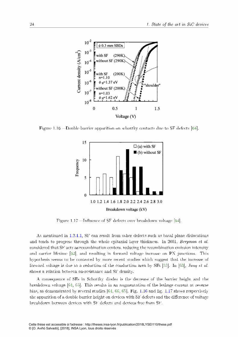
24 1. State of the art in SiC devices
Figure 1.16 Double barrier apparition on schottky contacts due to SF defects [64].
Figure 1.17 Inuence of SF defects over breakdown voltage [64].
As mentioned in 1.2.1.1, SF can result from other defects such as basal plane dislocationsand tends to progress through the whole epitaxial layer thickness. In 2001, Bergman et al.considered that SF acts as recombination centers, reducing the recombination emission intensityand carrier lifetime [62], and resulting in forward voltage increase on PN junctions. Thishypothesis seems to be contested by more recent studies which suggest that the increase offorward voltage is due to a reduction of the conduction area by SFs [53]. In [63], Jung et al.shows a relation between on-resistance and SF density.
A consequence of SFs in Schottky diodes is the decrease of the barrier height and thebreakdown voltage [64, 65]. This results in an augmentation of the leakage current at reversebias, as demonstrated by several studies [64, 66, 65]. Fig. 1.16 and g. 1.17 shows respectivelythe apparition of a double barrier height on devices with SF defects and the dierence of voltagebreakdown between devices with SF defects and devices free from SF.
Cette thèse est accessible à l'adresse : http://theses.insa-lyon.fr/publication/2018LYSEI110/these.pdf © [O. Aviñó Salvadó], [2018], INSA Lyon, tous droits réservés

1.2. Impact of crystallographic defects in SiC 25
h992 h993 h994 h995 h997h”
2”
3”
3jFmm35Fmm
5jFmm
75Fmm
h999
4”hjjFmm
6”
8”
h5jFmm
2jjFmm
2jj9 2jh5
Tairov andFTsvetkovF– h978CreeFIncFfoundedF– h987FFistFCommercialFSiCFSubstrateF– h992FRAFFprocessFDPFNakamuraFMFetFalPMF– 2jj4FZeroFMicropipe .ZMPTMNFhjjmmFSubstrateF– 2jj62jjmmFSubstrateF– 2jh5F
Micropipes – majorFdefect
DislocationsFreduction
SurfaceFandFshapeFimprovements
25Fmm
Figure 1.18 Evolution of SiC Wolfspeed wafers from early 90's to present [54].
It is worth noting that SFs propagation incidence can be augmented under conditions ofhigh current density or high temperature operation [53].
1.2.2 SiC defects summary
Diculties to reach high crystal quality has long limited SiC development and expansion.Improvements on crystal growth techniques proposed by Tairov et al. [67] in 1978 representedan important step on SiC devices evolution. Semiconductor industries have focused on SiCdevices development at the end of the 80's.
DefectDensity (cm−2)Year 2012 [68]
Density (cm−2)Year 2016 [69]
Yield eect Reliability eect
MP <2 <0.3 minor criticalTSD 103 200 medium mediumTED < 104 3100 none noneBPD < 103 800 none critical (bipolar)SF 1 - minor criticalAdditional Epitaxialdefects
1− 10 - medium medium
Technology defects 1− 10 - medium medium
Table 1.5 Overall defect situation on state of the art wafers.
A lot of eorts have been dedicated to reduce and minimize defects. Fig. 1.18 illustratesSiC wafer development and evolution. In the early 90's, SiC wafers had 25 mm diameter size.In early 2000's, wafer size reached 100 mm size in diameter. Nevertheless, defects density wasstill too high to develop reliable power devices. CREE developed its rst 100 mm substratewith zero micropipes defect (ZMP) in 2006 [54]. One of the main objectives was reached.
Cette thèse est accessible à l'adresse : http://theses.insa-lyon.fr/publication/2018LYSEI110/these.pdf © [O. Aviñó Salvadó], [2018], INSA Lyon, tous droits réservés
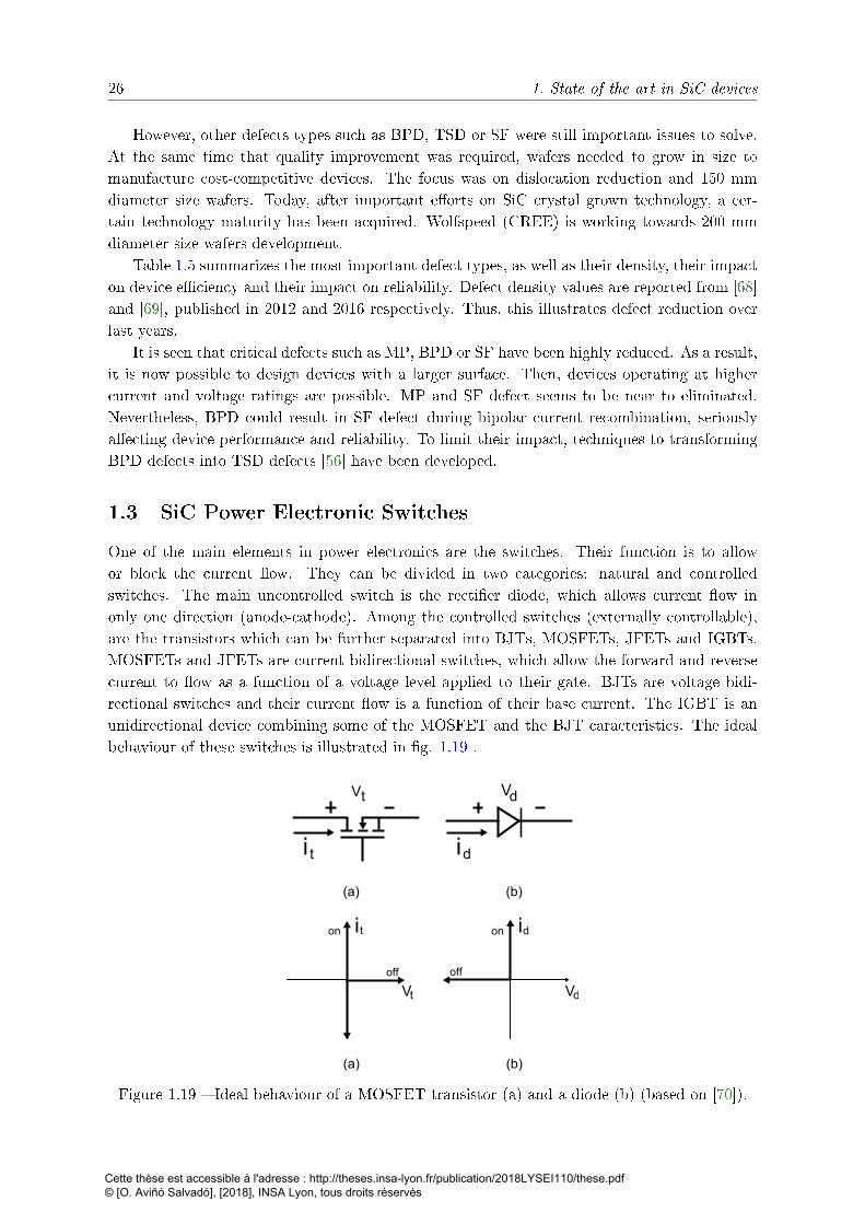
26 1. State of the art in SiC devices
However, other defects types such as BPD, TSD or SF were still important issues to solve.At the same time that quality improvement was required, wafers needed to grow in size tomanufacture cost-competitive devices. The focus was on dislocation reduction and 150 mmdiameter size wafers. Today, after important eorts on SiC crystal grown technology, a cer-tain technology maturity has been acquired. Wolfspeed (CREE) is working towards 200 mmdiameter size wafers development.
Table 1.5 summarizes the most important defect types, as well as their density, their impacton device eciency and their impact on reliability. Defect density values are reported from [68]and [69], published in 2012 and 2016 respectively. Thus, this illustrates defect reduction overlast years.
It is seen that critical defects such as MP, BPD or SF have been highly reduced. As a result,it is now possible to design devices with a larger surface. Then, devices operating at highercurrent and voltage ratings are possible. MP and SF defect seems to be near to eliminated.Nevertheless, BPD could result in SF defect during bipolar current recombination, seriouslyaecting device performance and reliability. To limit their impact, techniques to transformingBPD defects into TSD defects [56] have been developed.
1.3 SiC Power Electronic Switches
One of the main elements in power electronics are the switches. Their function is to allowor block the current ow. They can be divided in two categories: natural and controlledswitches. The main uncontrolled switch is the rectier diode, which allows current ow inonly one direction (anode-cathode). Among the controlled switches (externally controllable),are the transistors which can be further separated into BJTs, MOSFETs, JFETs and IGBTs.MOSFETs and JFETs are current bidirectional switches, which allow the forward and reversecurrent to ow as a function of a voltage level applied to their gate. BJTs are voltage bidi-rectional switches and their current ow is a function of their base current. The IGBT is anunidirectional device combining some of the MOSFET and the BJT caracteristics. The idealbehaviour of these switches is illustrated in g. 1.19 .
Vt
Vt
Vd
it
it
Vd
id
id
(a)
(a)
(b)
(b)
onon
off off
Figure 1.19 Ideal behaviour of a MOSFET transistor (a) and a diode (b) (based on [70]).
Cette thèse est accessible à l'adresse : http://theses.insa-lyon.fr/publication/2018LYSEI110/these.pdf © [O. Aviñó Salvadó], [2018], INSA Lyon, tous droits réservés
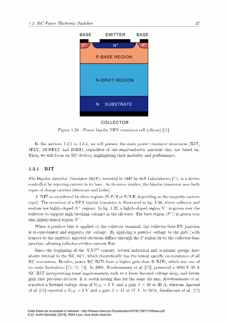
1.3. SiC Power Electronic Switches 27
COLLECTOR
N-DRIFT REGION
P-BASE REGION
N SUBSTRATE
BASE BASEEMITTER
N+ P+P+
Figure 1.20 Power bipolar NPN transistor cell (silicon) [21].
In the sections 1.3.1 to 1.3.4, we will present the main power transistor structures (BJT,JFET, MOSFET and IGBT), regardless of the semiconductor material they are based on.Then, we will focus on SiC devices, highlighting their maturity and performance.
1.3.1 BJT
The Bipolar Junction Transistor (BJT), invented in 1947 by Bell Laboratories [71], is a devicecontrolled by injecting current in its base. As its name implies, the bipolar transistor uses bothtypes of charge carriers (electrons and holes).
A BJT is constituted by three regions (N-P-N or P-N-P, depending on the majority carrierstype). The structure of a NPN bipolar transistor is illustrated in g. 1.20, where collector andemitter are highly-doped N+ regions. In g. 1.20, a lightly-doped region N− is grown over thecollector to support high blocking voltages in the o-state. The base region (P−) is grown overthis lightly-doped region N−.
When a positive bias is applied to the collector terminal, the collector-base PN junctionis reverse-biased and supports the voltage. By applying a positive voltage to the gate (withrespect to the emitter), injected electrons diuse through the P region up to the collector-basejunction, allowing collector-emitter current ow.
Since the beginning of the XXIth century, several industrial and academic groups haveshown interest in the SiC BJT, which theoretically has the lowest specic on-resistance of allSiC transistors. Besides, power SiC BJTs have a higher gain than Si BJTs, which was one ofits main limitations [72, 73, 74]. In 2005, Krishnaswami et al. [75], presented a 1000 V 30 ASiC BJT incorporating some improvements, such as a lower forward voltage drop, and bettergain that previous devices. It is worth noting that for the same die size, Krishnaswami et al.reported a forward voltage drop of VCE = 2 V and a gain β = 40 at 30 A, whereas Agarwalet al. [76] reported a VCE = 2 V and a gain β = 11 at 17 A. In 2013, Sundaresan et al. [77]
Cette thèse est accessible à l'adresse : http://theses.insa-lyon.fr/publication/2018LYSEI110/these.pdf © [O. Aviñó Salvadó], [2018], INSA Lyon, tous droits réservés
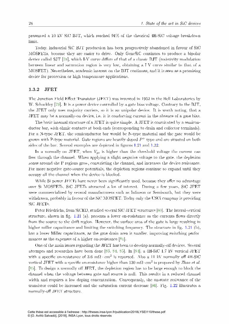
28 1. State of the art in SiC devices
presented a 10 kV SiC BJT, which reached 91% of the theorical 4H-SiC voltage breakdownlimit.
Today, industrial SiC BJT production has been progressively abandoned in favour of SiCMOSFETs, because they are easier to drive. Only GeneSiC continues to produce a bipolardevice called SJT [78], which I-V curve diers of that of a classic BJT (resistivity modulationbetween linear and saturation region is very low, obtaining a I-V curve similar to that of aMOSFET). Nevertheless, academic interest on the BJT continues, and it is seen as a promisingdevice for protection or high temperature applications.
1.3.2 JFET
The Junction Field Eect Transistor (JFET) was invented in 1952 in the Bell Laboratories byW. Schockley [79]. It is a power device controlled by a gate bias voltage. Contrary to the BJT,the JFET only uses majority carriers, so it is an unipolar device. It is worth noting, that aJFET may be a normally-on device, i.e. it is conducting current in the absence of a gate bias.
The basic internal structure of a JFET is quite simple. A JFET is constituted by a semicon-ductor bar, with ohmic contacts at both ends (corresponding to drain and collector terminals).For a N-type JFET, the semiconductor bar would be N-type material and the gate would begrown with P-type material. Gate regions are heavily doped P+ type and are situated on bothsides of the bar. Several examples are depicted in gures 1.21 and 1.22.
In a normally-on JFET, when Vgs is higher than the threshold voltage the current canow through the channel. When applying a slight negative voltage to the gate, the depletionzones around the P regions grow, constricting the channel, and increases the device resistance.For more negative gate-source potentials, the depletion regions continue to expand until theyoccupy all the channel when the device is blocked.
While Si power JFETs have never been signicantly used, because they oer no advantageover Si MOSFETs, SiC JFETs attracted a lot of interest. During a few years, SiC JFETwere commercialized by several manufacturers such as Inneon or Semisouth, but they werewithdrawn, probably in favour of the SiC MOSFET. Today only the USCi company is providingSiC JFETs.
Peter Friedrichs, from SiCED, studied several SiC JFET structures [80]. The lateral-verticalstructure, shown in g. 1.21 (a), presents a lower on-resistance as the currents ows directlyfrom the source to the drift region. However, the surface area of the gate is large resulting inhigher miller capacitance and limiting the switching frequency. The structure in g. 1.21 (b),has a lower Miller capacitance, as the gate-drain area is smaller, improving switching perfor-mances as the expenses of a higher on-resistance [81].
One of the main issues regarding the JFET has been to develop normally-o devices. Severalattempts and researches have been done [83, 84, 85]. In [84], a 4H-SiC 1.7 kV vertical JFETwith a specic on-resistance of 3.6 mΩ · cm2 is reported. Also a 11 kV normally o 4H-SiCvertical JFET with a specic on-resistance higher than 130 mΩ · cm2 is proposed by Zhao et al.[85]. To design a normally-o JFET, the depletion region has to be large enough to block thechannel when the voltage between gate and source is null. This results in a reduced channelwidth and requires a low doping concentration. Consequently, the on-state resistance of thetransistor could be increased and the saturation current decrease [86]. Fig. 1.22 illustrates anormally-o JFET structure.
Cette thèse est accessible à l'adresse : http://theses.insa-lyon.fr/publication/2018LYSEI110/these.pdf © [O. Aviñó Salvadó], [2018], INSA Lyon, tous droits réservés
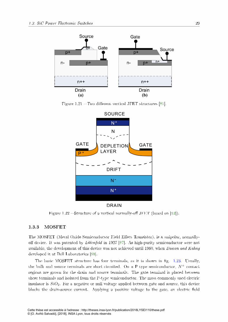
1.3. SiC Power Electronic Switches 29
n+
n+
Figure 1.21 Two dierent vertical JFET structures [81].
N
DRAIN
DRIFT
DEPLETIONLAYER
GATE
SOURCE
GATE
+
N
N
+
N -
P +
Figure 1.22 Structure of a vertical normally-o JFET (based on [82]).
1.3.3 MOSFET
The MOSFET (Metal Oxide Semiconductor Field Eect Transistor), is a unipolar, normally-o device. It was patented by Lilienfeld in 1927 [87]. As high-purity semiconductor were notavailable, the development of this device was not achieved until 1960, when Dawon and Kahngdeveloped it at Bell Laboratories [88].
The basic MOSFET structure has four terminals, as it is shown in g. 1.23. Usually,the bulk and source terminals are short-circuited. On a P-type semiconductor, N+ contactregions are grown for the drain and source terminals. The gate terminal is placed betweenthese terminals and isolated from the P-type semiconductor. The most commonly used electricinsulator is SiO2. For a negative or null voltage applied between gate and source, this deviceblocks the drain-source current. Applying a positive voltage to the gate, an electric eld
Cette thèse est accessible à l'adresse : http://theses.insa-lyon.fr/publication/2018LYSEI110/these.pdf © [O. Aviñó Salvadó], [2018], INSA Lyon, tous droits réservés
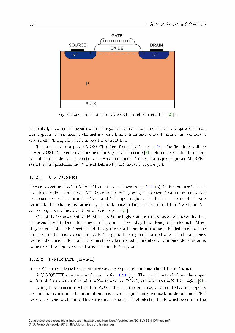
30 1. State of the art in SiC devices
N+ N+
OXIDE
BULK
SOURCE
GATE
P
++++++++++++++
DRAIN
Figure 1.23 Basic Silicon MOSFET structure (based on [21]).
is created, causing a concentration of negative charges just underneath the gate terminal.For a given electric eld, a channel is created, and drain and source terminals are connectedelectrically. Then, the device allows the current ow.
The structure of a power MOSFET diers from that in g. 1.23. The rst high-voltagepower MOSFETs were developed using a V-groove structure [21]. Nevertheless, due to techni-cal diculties, the V-groove structure was abandoned. Today, two types of power MOSFETstructure are predominant: Vertical-Diused (VD) and trench-gate (U).
1.3.3.1 VD-MOSFET
The cross section of a VD-MOSFET structure is shown in g. 1.24 (a). This structure is basedon a heavily-doped substrate N+. Over this, a N− type layer is grown. Two ion implantationprocessus are used to form the P-well and N+ doped regions, situated at each side of the gateterminal. The channel is formed by the dierence in lateral extension of the P-well and N+source regions produced by their diusion cycles [21].
One of the inconvenient of this structure is the higher on-state resistance. When conducting,electrons circulate from the source to the drain. First, they ow through the channel. After,they enter in the JFET region and nally they reach the drain through the drift region. Thehigher on-state resistance is due to JFET region. This region is located where the P-well zonesrestrict the current ow, and care must be taken to reduce its eect. One possible solution isto increase the doping concentration in the JFET region.
1.3.3.2 U-MOSFET (Trench)
In the 90's, the U-MOSFET structure was developed to eliminate the JFET resistance.
A U-MOSFET structure is showed in g. 1.24 (b). The trench extends from the uppersurface of the structure through the N+ source and P-body regions into the N-drift region [21].
Using this structure, when the MOSFET is in the on-state, a vertical channel appearsaround the trench and the internal on-resistance is signicantly reduced, as there is no JFETresistance. One problem of this structure is that the high electric elds which occurs in the
Cette thèse est accessible à l'adresse : http://theses.insa-lyon.fr/publication/2018LYSEI110/these.pdf © [O. Aviñó Salvadó], [2018], INSA Lyon, tous droits réservés
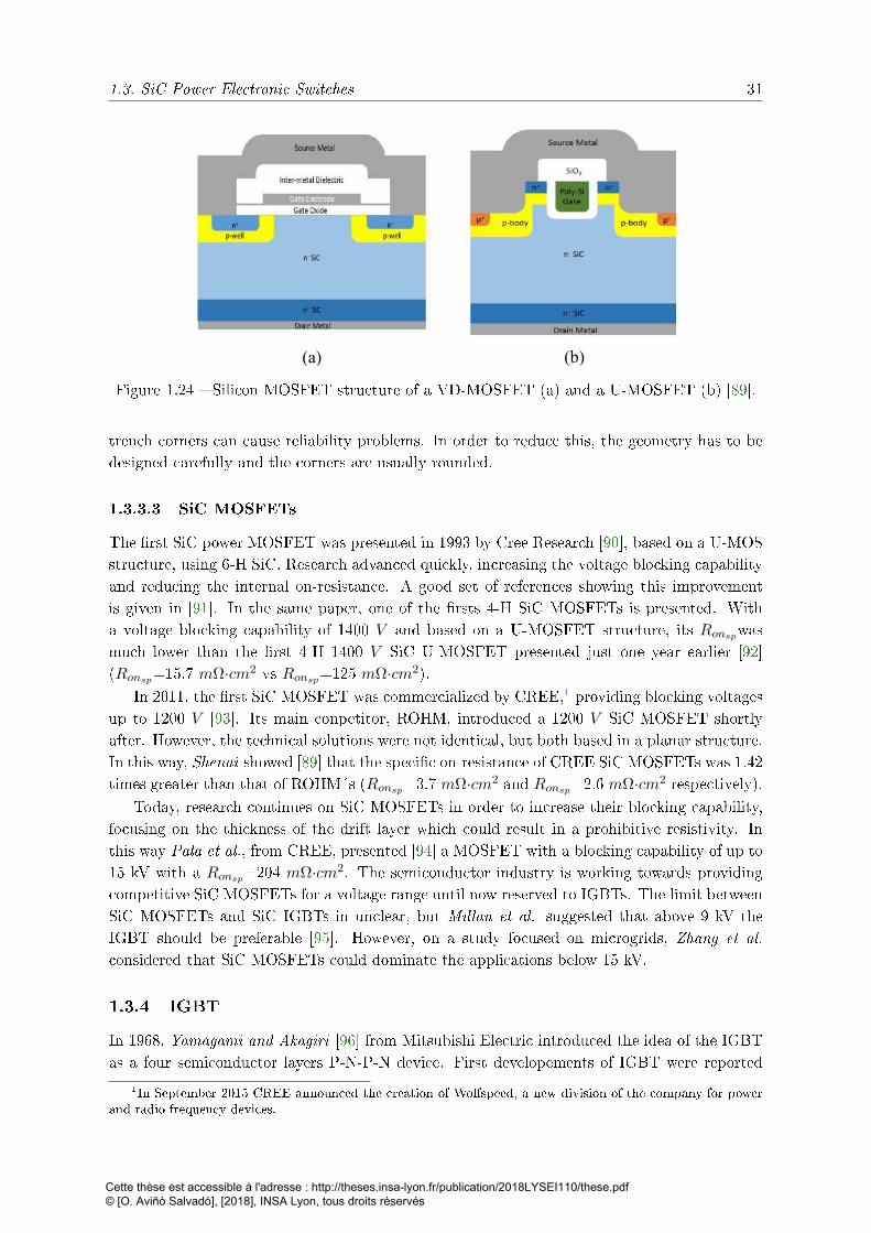
1.3. SiC Power Electronic Switches 31
(a) (b)
Figure 1.24 Silicon MOSFET structure of a VD-MOSFET (a) and a U-MOSFET (b) [89].
trench corners can cause reliability problems. In order to reduce this, the geometry has to bedesigned carefully and the corners are usually rounded.
1.3.3.3 SiC MOSFETs
The rst SiC power MOSFET was presented in 1993 by Cree Research [90], based on a U-MOSstructure, using 6-H SiC. Research advanced quickly, increasing the voltage blocking capabilityand reducing the internal on-resistance. A good set of references showing this improvementis given in [91]. In the same paper, one of the rsts 4-H SiC MOSFETs is presented. Witha voltage blocking capability of 1400 V and based on a U-MOSFET structure, its Ronspwasmuch lower than the rst 4-H 1400 V SiC U-MOSFET presented just one year earlier [92](Ronsp=15.7 mΩ·cm2 vs Ronsp=125 mΩ·cm2).
In 2011, the rst SiC MOSFET was commercialized by CREE,1 providing blocking voltagesup to 1200 V [93]. Its main conpetitor, ROHM, introduced a 1200 V SiC MOSFET shortlyafter. However, the technical solutions were not identical, but both based in a planar structure.In this way, Shenai showed [89] that the specic on-resistance of CREE SiC MOSFETs was 1.42times greater than that of ROHM´s (Ronsp=3.7 mΩ·cm2 and Ronsp=2.6 mΩ·cm2 respectively).
Today, research continues on SiC MOSFETs in order to increase their blocking capability,focusing on the thickness of the drift layer which could result in a prohibitive resistivity. Inthis way Pala et al., from CREE, presented [94] a MOSFET with a blocking capability of up to15 kV with a Ronsp=204 mΩ·cm2. The semiconductor industry is working towards providingcompetitive SiC MOSFETs for a voltage range until now reserved to IGBTs. The limit betweenSiC MOSFETs and SiC IGBTs in unclear, but Millan et al. suggested that above 9 kV theIGBT should be preferable [95]. However, on a study focused on microgrids, Zhang et al.considered that SiC MOSFETs could dominate the applications below 15 kV.
1.3.4 IGBT
In 1968, Yamagami and Akagiri [96] from Mitsubishi Electric introduced the idea of the IGBTas a four semiconductor layers P-N-P-N device. First developements of IGBT were reported
1In September 2015 CREE announced the creation of Wolfspeed, a new division of the company for powerand radio frequency devices.
Cette thèse est accessible à l'adresse : http://theses.insa-lyon.fr/publication/2018LYSEI110/these.pdf © [O. Aviñó Salvadó], [2018], INSA Lyon, tous droits réservés
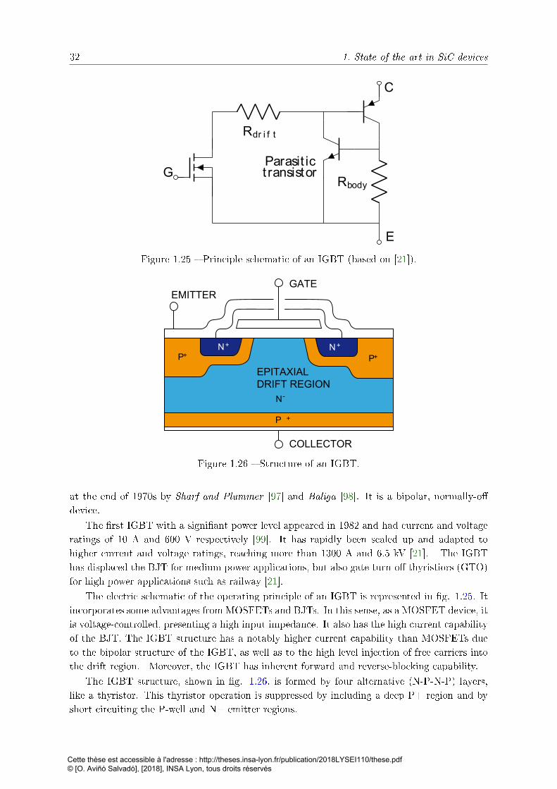
32 1. State of the art in SiC devices
Rdr i f t
C
Rbody
E
GParasit ict ransistor
Figure 1.25 Principle schematic of an IGBT (based on [21]).
P+
COLLECTOR
EPITAXIALDRIFT REGION
+
N+
N
P
-
P+N+
EMITTERGATE
Figure 1.26 Structure of an IGBT.
at the end of 1970s by Sharf and Plummer [97] and Baliga [98]. It is a bipolar, normally-odevice.
The rst IGBT with a signiant power level appeared in 1982 and had current and voltageratings of 10 A and 600 V respectively [99]. It has rapidly been scaled up and adapted tohigher current and voltage ratings, reaching more than 1300 A and 6.5 kV [21]. The IGBThas displaced the BJT for medium power applications, but also gate turn-o thyristiors (GTO)for high power applications such as railway [21].
The electric schematic of the operating principle of an IGBT is represented in g. 1.25. Itincorporates some advantages from MOSFETs and BJTs. In this sense, as a MOSFET device, itis voltage-controlled, presenting a high input impedance. It also has the high current capabilityof the BJT. The IGBT structure has a notably higher current capability than MOSFETs dueto the bipolar structure of the IGBT, as well as to the high level injection of free carriers intothe drift region. Moreover, the IGBT has inherent forward and reverse-blocking capability.
The IGBT structure, shown in g. 1.26, is formed by four alternative (N-P-N-P) layers,like a thyristor. This thyristor operation is suppressed by including a deep P+ region and byshort circuiting the P-well and N+ emitter regions.
Cette thèse est accessible à l'adresse : http://theses.insa-lyon.fr/publication/2018LYSEI110/these.pdf © [O. Aviñó Salvadó], [2018], INSA Lyon, tous droits réservés
1.3. SiC Power Electronic Switches 33
For a null gate-emitter voltage, the IGBT is blocked. Applying a voltage higher than thethreshold voltage, a channel appears between the N+ and N drift regions, allowing current toow from the P-N-P bipolar structure. Therefore, the collector-emitter current is the sum fromthat of the bipolar P-N-P structure and of the unipolar MOSFET structure.
Even if SiC IGBTs are not commercially available yet, they attract a lot of research eort.They are not competitive against SiC MOSFETs for relatively low-medium voltages (<9 kV)due to the collector-emitter voltage drop in the saturation region. Ruy et al., from Cree,reported on 2012 a 4-H SiC N-IGBT with a voltage blocking capability of 12.5 kV with aVcesat=6.1 V for a current of 32 A and Vge=20 V [100]. In 2014, Van Brunt et al. reportedthe IGBT with the higher blocking capability in our knowledge, reaching 27 kV [101] with aVcesat=11.8 V for a current of 20 A and Vge=20 V .
1.3.5 Comparison of SiC devices
Until today, the IGBT has been the principal device for high power applications due to Sitechnology limitations. With the apparition of SiC devices, BJT, JFET or MOSFET role hasto be re-evaluated as they can be good alternatives for relatively high power applications (inthe hundreds of kVA) such as railway or aeronautics. Besides, the Si IGBT is the more complexand expensive of all those devices and presents frequency limitations (few tens of kHz).
Among SiC devices, BJT is an interesting low cost alternative, as it has the lower specicon-resistance, and can operate at relatively high frequencies (commutation time in the order of100 ns [102]). Nevertheless, it has some drawbacks. It requires a permanent base-current exci-tation. This is contrary to industries preferences for high input impedance (voltage-controlleddevices). This would require to develop specic drivers. Moreover, current gain presents impor-tant limitations mainly due to SiC substrate defects and surface recombination centers, whichincrease the device resistance limiting its gain [103, 104]. Today, oxide passivation is limitingthe gain current on SiC BJT [105].
JFETs and MOSFETs are medium-cost alternatives, capable to operate at high frequencies(near 1 MHz). They are voltage controlled devices, thanks to their high gate input impedance.JFETs, as explained early are normally-on devices. Then, a loss of a gate driver signal couldresult in a system damage. For this reason, the MOSFET is preferred for most of the powerelectronic applications in its power range.
However, the MOSFET is a more complex device than the JFET and presents some addi-tional reliability issues relative to the gate oxide insulator (SiO2). These reliability problems,presented in detail in the following sections, are basically due to threshold voltage instabilityand oxide degradation or even failure under conditions of high electric elds and temperature[106]. In this case, electric charges can be injected in or through the Si/SiO2 interface, accel-erating its degradation or causing voltage threshold instability and result in a change in the aoperation conditions.
Therefore, as the SiC MOSFET is the preferred controlled switch for applications whichwere until today reserved to the Si IGBT, a special care has to be given to the MOSFETreliability to insure industry quality standards and systems lifetime requirements [107].
Cette thèse est accessible à l'adresse : http://theses.insa-lyon.fr/publication/2018LYSEI110/these.pdf © [O. Aviñó Salvadó], [2018], INSA Lyon, tous droits réservés

34 1. State of the art in SiC devices
1.4 SiC MOSFET robustness issues
The objective of this thesis is to study the robustness of SiC MOSFETs under several conditionsof operation. Due to the defects, SiC devices reliability has been highly discussed for a longtime. As presented in section 1.2, the defect density has drastically reduced in the wafer. Thus,it is time to evaluate if present SiC devices are reliable, and if they are ready to be used onindustrial applications.
On the following pages, a review of the most important reliability issues remaining associatedwith SiC devices is shown:
Gate MOSFET robustness.
Internal diode robustness.
Robustness under avalanche breakdown phenomenon.
Robustness under short-circuit conditions.
1.4.1 Gate robustness
Gate robustness is probably the most important reliability issue for SiC MOSFETs devices.Indeed, this issue concerns specially MOSFETs because it is mainly related to the SiO2 gateinsulator. Other devices, such as JFETs or BJTs, do not have this gate oxide and are notconcerned by this issue.
The physical phenomenon associated with gate reliability are presented in section 1.4.1.1.The main measurements to evaluate the gate oxide degradation are described in section 1.4.1.2and 1.4.1.3. They are:
Time Dependent Dielectric Breakdown - TDDB
Bias Temperature Instability - NBTI/PBTI
1.4.1.1 Energy band and carrier injection phenomenons
Energy band diagrams are common representation of semiconductor structures where conduc-tion and valence band are dened. Electrons are lling the valence band and only a few arelocated in the conduction band. Only the electrons of the conduction band participate inthe conduction of the device. Electrons placed in the valence band can reach the conductionband, providing they a level of energy equivalent to the energy bandgap, which is the dier-ence between the energy levels of the conduction and valence bands. This is possible throughvarious excitations as heat (phonon) or light (photon) excitations. Electrons can not be placedin-between the valence and the conduction bands except for deep traps.
As every semiconductor has dierent electrical properties, its energy band diagram it isalso dierent. Fig. 1.27 shows the energy bands for dierent semiconductor materials anddielectrics. It can be seen that SiO2 bandgap is 9 eV and 3.2 eV for 4H-SiC. Si has a muchlower bandgap, at 1.1 eV. Therefore, the barrier height between 4H-SiC and SiO2 conductionbands is lower and results 2.7 eV for 4H-SiC (in comparison with 3.2 eV for Si).
In g. 1.28, a schematic energy band diagram is represented with a 4H-SiC (blue) semi-conductor and SiO2 interface. Moreover, silicon energy bands (brown) and the main carrier
Cette thèse est accessible à l'adresse : http://theses.insa-lyon.fr/publication/2018LYSEI110/these.pdf © [O. Aviñó Salvadó], [2018], INSA Lyon, tous droits réservés
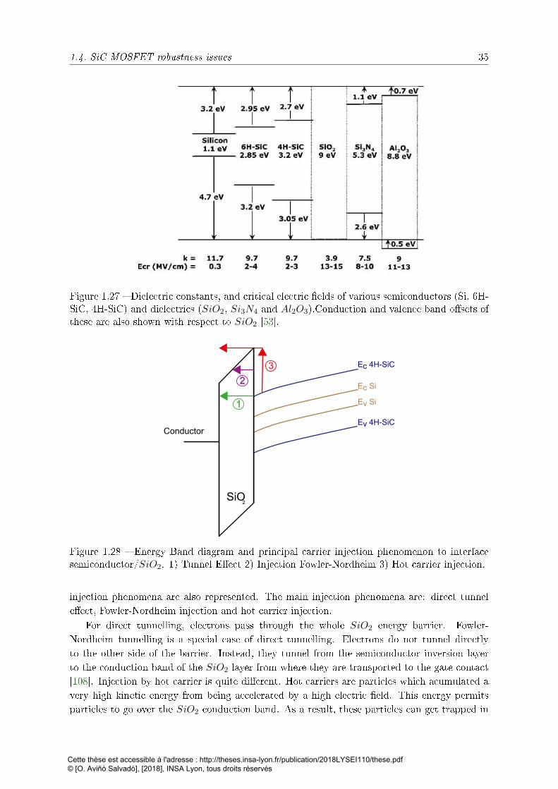
1.4. SiC MOSFET robustness issues 35
Figure 1.27 Dielectric constants, and critical electric elds of various semiconductors (Si, 6H-SiC, 4H-SiC) and dielectrics (SiO2, Si3N4 and Al2O3).Conduction and valence band osets ofthese are also shown with respect to SiO2 [53].
Conductor
SiO
3
2
2
1
Ec 4H-SiC
Ev 4H-SiC
Ev Si
Ec Si
Figure 1.28 Energy Band diagram and principal carrier injection phenomenon to interfacesemiconductor/SiO2. 1) Tunnel Eect 2) Injection Fowler-Nordheim 3) Hot carrier injection.
injection phenomena are also represented. The main injection phenomena are: direct tunneleect, Fowler-Nordheim injection and hot carrier injection.
For direct tunnelling, electrons pass through the whole SiO2 energy barrier. Fowler-Nordheim tunnelling is a special case of direct tunnelling. Electrons do not tunnel directlyto the other side of the barrier. Instead, they tunnel from the semiconductor inversion layerto the conduction band of the SiO2 layer from where they are transported to the gate contact[108]. Injection by hot carrier is quite dierent. Hot carriers are particles which acumulated avery high kinetic energy from being accelerated by a high electric eld. This energy permitsparticles to go over the SiO2 conduction band. As a result, these particles can get trapped in
Cette thèse est accessible à l'adresse : http://theses.insa-lyon.fr/publication/2018LYSEI110/these.pdf © [O. Aviñó Salvadó], [2018], INSA Lyon, tous droits réservés
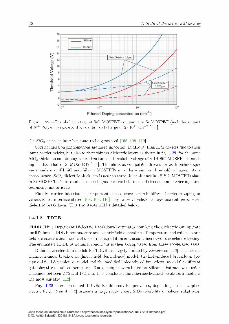
36 1. State of the art in SiC devices
Figure 1.29 Threshold voltage of SiC MOSFET compared to Si MOSFET (includes impactof N+ Polysilicon gate and an oxide xed charge of 2 · 1011 cm−2 [111].
the SiO2 or cause interface state to be generated [108, 109, 110].
Carrier injection phenomenons are more important in 4H-SiC than in Si devices due to theirlower barrier height, but also to their thinner dielectric layer: as shown in g. 1.29, for the sameSiO2 thickness and doping concentration, the threshold voltage of a 4H-SiC MOSFET is muchhigher than that of Si MOSFETs [111]. Therefore, as compatible drivers for both technologiesare mandatory, 4H-SiC and Silicon MOSFETs must have similar threshold voltages. As aconsequence, SiO2 dielectric thickness is near to three times thinner in 4H-SiC MOSFETs thanin Si MOSFETs. This result in much higher electric eld in the dielectric, and carrier injectionbecomes a major issue.
Finally, carrier injection has important consequences on reliability. Carrier trapping orgeneration of interface states [108, 109, 110] may cause threshold voltage instabilities or evendielectric breakdown. This two issues will be detailed below.
1.4.1.2 TDDB
TDDB (Time Dependent Dielectric Breakdown) estimates how long the dielectric can operateuntil failure. TDDB is temperature and electric eld dependent. Temperature and oxide electriceld are acceleration factors of dielectric degradation and usually increased to accelerate testing.The estimated TDDB at nominal conditions is then extrapolated from these accelerated tests.
Dierent acceleration models for TDDB are largely studied by Kimura on [112], such as thethermochemical breakdown (linear eld dependence) model, the hole-induced breakdown (re-ciprocal eld dependence) model and the modied hole-induced breakdown model for dierentgate bias stress and temperatures. Tested samples were based on Silicon substrates with oxidethickness between 2.75 and 18.1 nm. It is concluded that thermochemical breakdown model isthe most suitable [112].
Fig. 1.30 shows predicted TDDBs for dierent temperatures, depending on the appliedelectric eld. Even if [112] presents a large study about SiO2 reliability on silicon substrates,
Cette thèse est accessible à l'adresse : http://theses.insa-lyon.fr/publication/2018LYSEI110/these.pdf © [O. Aviñó Salvadó], [2018], INSA Lyon, tous droits réservés
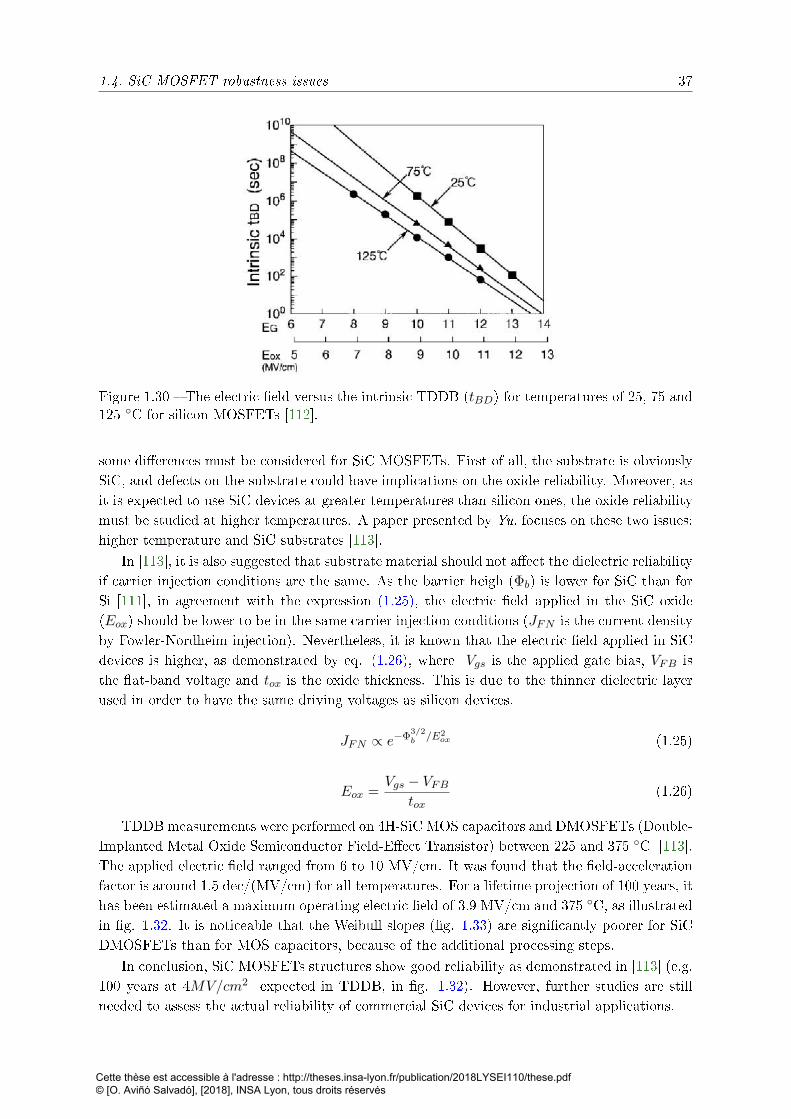
1.4. SiC MOSFET robustness issues 37
Figure 1.30 The electric eld versus the intrinsic TDDB (tBD) for temperatures of 25, 75 and125 C for silicon MOSFETs [112].
some dierences must be considered for SiC MOSFETs. First of all, the substrate is obviouslySiC, and defects on the substrate could have implications on the oxide reliability. Moreover, asit is expected to use SiC devices at greater temperatures than silicon ones, the oxide reliabilitymust be studied at higher temperatures. A paper presented by Yu, focuses on these two issues:higher temperature and SiC substrates [113].
In [113], it is also suggested that substrate material should not aect the dielectric reliabilityif carrier injection conditions are the same. As the barrier heigh (Φb) is lower for SiC than forSi [111], in agreement with the expression (1.25), the electric eld applied in the SiC oxide(Eox) should be lower to be in the same carrier injection conditions (JFN is the current densityby Fowler-Nordheim injection). Nevertheless, it is known that the electric eld applied in SiCdevices is higher, as demonstrated by eq. (1.26), where Vgs is the applied gate bias, VFB isthe at-band voltage and tox is the oxide thickness. This is due to the thinner dielectric layerused in order to have the same driving voltages as silicon devices.
JFN ∝ e−Φ3/2b /E2
ox (1.25)
Eox =Vgs − VFB
tox(1.26)
TDDB measurements were performed on 4H-SiC MOS capacitors and DMOSFETs (Double-Implanted Metal Oxide Semiconductor Field-Eect Transistor) between 225 and 375 C [113].The applied electric eld ranged from 6 to 10 MV/cm. It was found that the eld-accelerationfactor is around 1.5 dec/(MV/cm) for all temperatures. For a lifetime projection of 100 years, ithas been estimated a maximum operating electric eld of 3.9 MV/cm and 375 C, as illustratedin g. 1.32. It is noticeable that the Weibull slopes (g. 1.33) are signicantly poorer for SiCDMOSFETs than for MOS capacitors, because of the additional processing steps.
In conclusion, SiC MOSFETs structures show good reliability as demonstrated in [113] (e.g.100 years at 4MV/cm2 expected in TDDB, in g. 1.32). However, further studies are stillneeded to assess the actual reliability of commercial SiC devices for industrial applications.
Cette thèse est accessible à l'adresse : http://theses.insa-lyon.fr/publication/2018LYSEI110/these.pdf © [O. Aviñó Salvadó], [2018], INSA Lyon, tous droits réservés
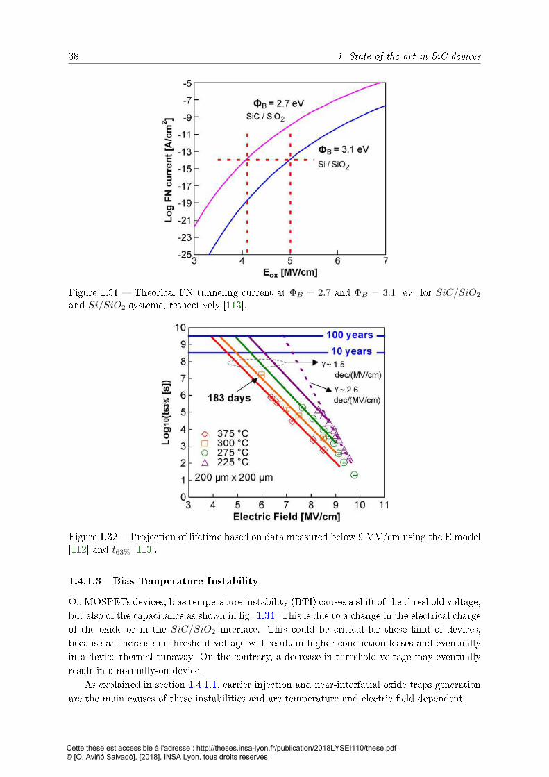
38 1. State of the art in SiC devices
Figure 1.31 Theorical FN tunneling current at ΦB = 2.7 and ΦB = 3.1 ev for SiC/SiO2
and Si/SiO2 systems, respectively [113].
Figure 1.32 Projection of lifetime based on data measured below 9 MV/cm using the E model[112] and t63% [113].
1.4.1.3 Bias Temperature Instability
OnMOSFETs devices, bias temperature instability (BTI) causes a shift of the threshold voltage,but also of the capacitance as shown in g. 1.34. This is due to a change in the electrical chargeof the oxide or in the SiC/SiO2 interface. This could be critical for these kind of devices,because an increase in threshold voltage will result in higher conduction losses and eventuallyin a device thermal runaway. On the contrary, a decrease in threshold voltage may eventuallyresult in a normally-on device.
As explained in section 1.4.1.1, carrier injection and near-interfacial oxide traps generationare the main causes of these instabilities and are temperature and electric eld dependent.
Cette thèse est accessible à l'adresse : http://theses.insa-lyon.fr/publication/2018LYSEI110/these.pdf © [O. Aviñó Salvadó], [2018], INSA Lyon, tous droits réservés
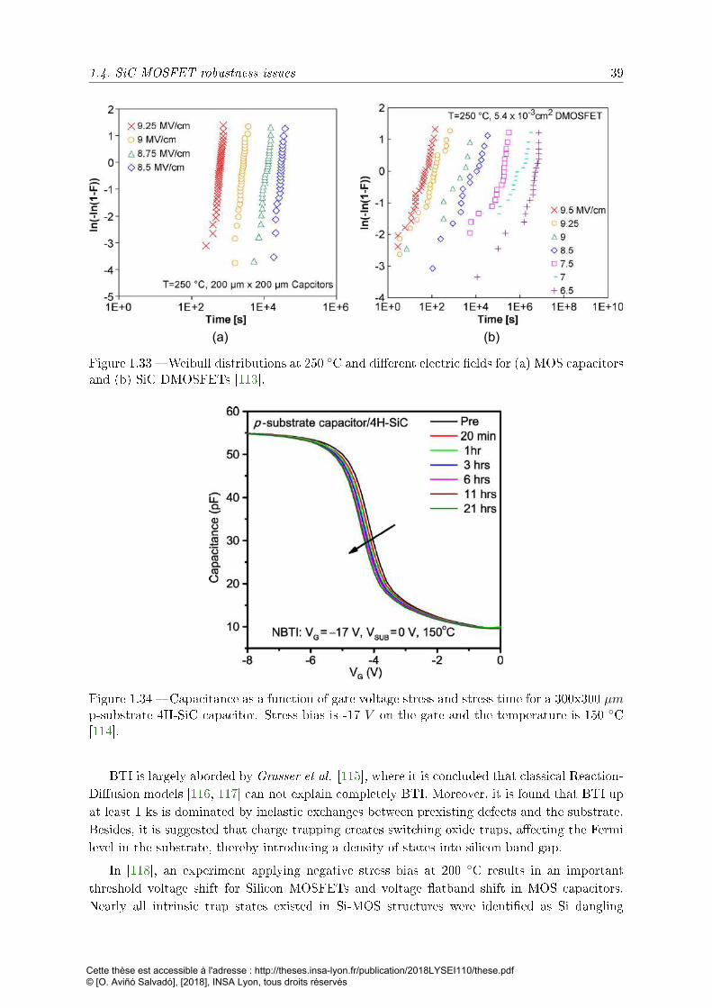
1.4. SiC MOSFET robustness issues 39
(a) (b)
Figure 1.33 Weibull distributions at 250 C and dierent electric elds for (a) MOS capacitorsand (b) SiC DMOSFETs [113].
Figure 1.34 Capacitance as a function of gate voltage stress and stress time for a 300x300 µmp-substrate 4H-SiC capacitor. Stress bias is -17 V on the gate and the temperature is 150 C[114].
BTI is largely aborded by Grasser et al. [115], where it is concluded that classical Reaction-Diusion models [116, 117] can not explain completely BTI. Moreover, it is found that BTI upat least 1 ks is dominated by inelastic exchanges between prexisting defects and the substrate.Besides, it is suggested that charge trapping creates switching oxide traps, aecting the Fermilevel in the substrate, thereby introducing a density of states into silicon band gap.
In [118], an experiment applying negative stress bias at 200 C results in an importantthreshold voltage shift for Silicon MOSFETs and voltage atband shift in MOS capacitors.Nearly all intrinsic trap states existed in Si-MOS structures were identied as Si dangling
Cette thèse est accessible à l'adresse : http://theses.insa-lyon.fr/publication/2018LYSEI110/these.pdf © [O. Aviñó Salvadó], [2018], INSA Lyon, tous droits réservés
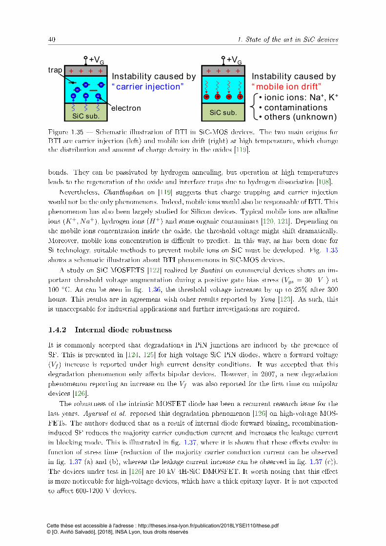
40 1. State of the art in SiC devices
Instability caused by“ carrier injection”
Instability caused by“ mobile ion drift”
SiC sub.• contaminations• ionic ions: Na+, K+
+ + + + + + + +
+ ++ +
SiC sub.
- - -
+VG +VG
-- -
trap
electron• others (unknown)
Figure 1.35 Schematic illustration of BTI in SiC-MOS devices. The two main origins forBTI are carrier injection (left) and mobile ion drift (right) at high temperature, which changethe distribution and amount of charge density in the oxides [119].
bonds. They can be passivated by hydrogen annealing, but operation at high temperaturesleads to the regeneration of the oxide and interface traps due to hydrogen dissociation [108].
Nevertheless, Chanthaphan on [119] suggests that charge trapping and carrier injectionwould not be the only phenomenons. Indeed, mobile ions would also be responsable of BTI. Thisphenomenon has also been largely studied for Silicon devices. Typical mobile ions are alkalineions (K+, Na+), hydrogen ions (H+) and some organic contaminats [120, 121]. Depending onthe mobile ions concentration inside the oxide, the threshold voltage might shift dramatically.Moreover, mobile ions concentration is dicult to predict. In this way, as has been done forSi technology, suitable methods to prevent mobile ions on SiC must be developed. Fig. 1.35shows a schematic illustration about BTI phenomenons in SiC-MOS devices.
A study on SiC MOSFETS [122] realized by Santini on commercial devices shows an im-portant threshold voltage augmentation during a positive gate bias stress (Vgs = 30 V ) at100 C. As can be seen in g. 1.36, the threshold voltage increases by up to 25% after 300hours. This results are in agreement with other results reported by Yang [123]. As such, thisis unacceptable for industrial applications and further investigations are required.
1.4.2 Internal diode robustness
It is commonly accepted that degradations in PiN junctions are induced by the presence ofSF. This is presented in [124, 125] for high voltage SiC PiN diodes, where a forward voltage(Vf ) increase is reported under high current density conditions. It was accepted that thisdegradation phenomenon only aects bipolar devices. However, in 2007, a new degradationphenomenon reporting an increase on the Vf was also reported for the rst time on unipolardevices [126].
The robustness of the intrinsic MOSFET diode has been a recurrent research issue for thelast years. Agarwal et al. reported this degradation phenomenon [126] on high-voltage MOS-FETs. The authors deduced that as a result of internal diode forward biasing, recombination-induced SF reduces the majority carrier conduction current and increases the leakage currentin blocking mode. This is illustrated in g. 1.37, where it is shown that these eects evolve infunction of stress time (reduction of the majority carrier conduction current can be observedin g. 1.37 (a) and (b), whereas the leakage current increase can be observed in g. 1.37 (c)).The devices under test in [126] are 10 kV 4H-SiC DMOSFET. It worth noting that this eectis more noticeable for high-voltage devices, which have a thick epitaxy layer. It is not expectedto aect 600-1200 V devices.
Cette thèse est accessible à l'adresse : http://theses.insa-lyon.fr/publication/2018LYSEI110/these.pdf © [O. Aviñó Salvadó], [2018], INSA Lyon, tous droits réservés
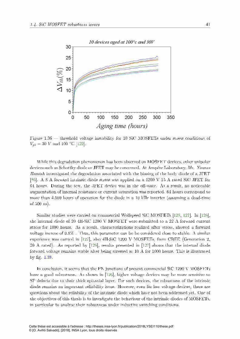
1.4. SiC MOSFET robustness issues 41
Figure 1.36 threshold voltage instability for 10 SiC MOSFETs under stress conditions ofVgs = 30 V and 100 C [122].
While this degradation phenomenon has been observed on MOSFET devices, other unipolardevices such as Schottky diode or JFET may be concerned. At Ampère Laboratory,Mr. YounesHamieh investigated the degradation associated with the biasing of the body diode of a JFET[86]. A 8 A forward intrinsic diode stress was applied on a 1200 V 15 A rated SiC JFET for64 hours. During the test, the JFET device was in the o-state. As a result, no noticeableaugmentation of internal resistance or current saturation was reported. 64 hours correspond tomore than 4,500 hours of operation for the diode in a 10 kHz inverter (assuming a dead-timeof 500 ns).
Similar studies were carried on commercial Wolfspeed SiC MOSFETs [128, 127]. In [128],the internal diode of 20 4H-SiC 1200 V MOSFET were submitted to a 22 A forward currentstress for 1000 hours. As a result, characterizations realized after stress, showed a forwardvoltage increse of 0.8% . Thus, this parameter can be be considered close to stable. A similarexperience was carried in [127], also 4H-SiC 1200 V MOSFETs, from CREE (Generation 2,20 A rated). As reported by [128], results presented in [127] shows that the internal diodeforward voltage remains stable after being stressed at 10 A for 1000 hours. This is illustratedby g. 1.38.
In conclusion, it seems that the PN junctions of present commercial SiC 1200 V MOSFETshave a good robustness. As shown in [126], higher voltage devices may be more sensitive toSF defects due to their thick epitaxial layer. For such devices, the robustness of the intrinsicdiode remains an important reliability issue. However, even for low voltage devices, there arequestions about the reliability of the intrinsic diode which have not been addressed yet. One ofthe objectives of this thesis is to investigate the behaviour of the intrinsic diodes of MOSFETs,in particular to analyse their robustness under inductive switching conditions.
Cette thèse est accessible à l'adresse : http://theses.insa-lyon.fr/publication/2018LYSEI110/these.pdf © [O. Aviñó Salvadó], [2018], INSA Lyon, tous droits réservés
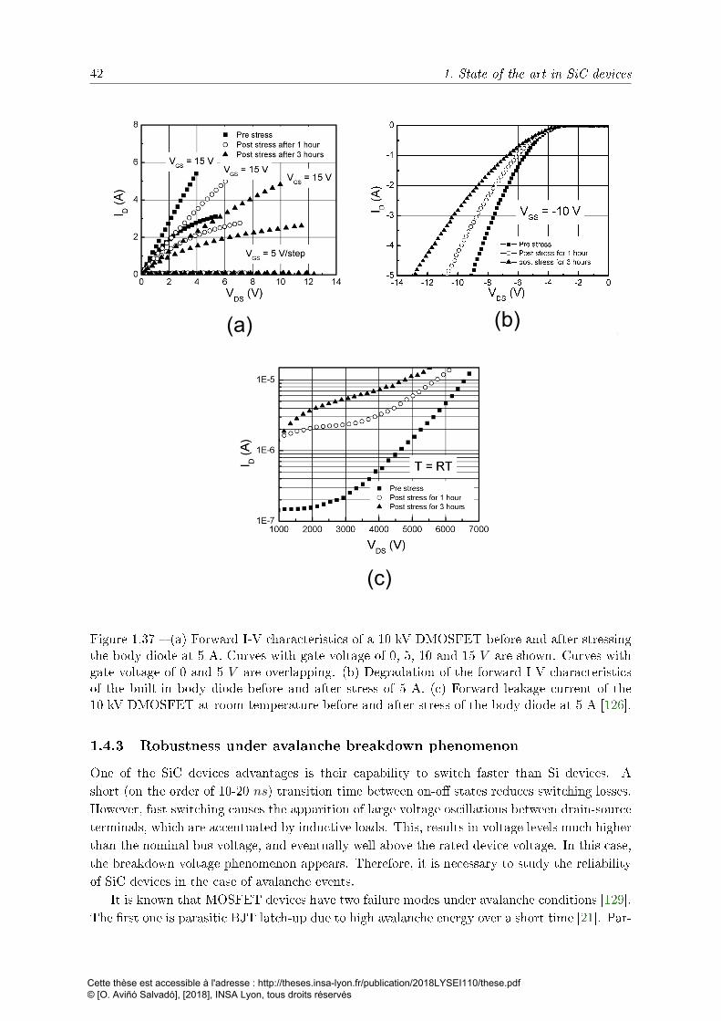
42 1. State of the art in SiC devices
Fig] 4] maC Forward I –V characteristics of the H7[kV DMOSFET before and after stressing the body diodHz V are shown] The curves with gate voltage of 7 and z V are overlapping] mbC Transfer characteristicsafter stress] mcC Forward leakage current of the H7[kV DMOSFETat room temperature before and after stres
well[understood phenomenon in SiCP caused by BPDs [H]–[W]P[A]] The MOSFET drift layer did not receive a BPD reductiontreatment] HenceP the lightly doped n[drift layer of the jH[SiCDMOSFEThad high density of BPDs]These dislocationstravelthe thicknessof the epilayer from substrate to the surface of thewafer where the device is made] When the p[n junction bodydiode is forward biasedP the electrons and holes recombine inthe drift layer]The recombination locally providesthe energy toactivate dislocation glide which gives rise to SFs [A]] The SFsshow up astriangular defects looking down at the surface of thedevice] The spatial size of the SFs depends upon the thicknessof the drift layer In this case the drift layer is H77[µm thick
results] It appearsbody diode not onlimpede the flow oby increased scatterinmobility of the carriercentration throughis not yet understoo
The leakage currenin Fig] 4mcC at roocurrent shows a marbody diode] Therecombination[induce
gradation of the forward I –V characteristics of the built[in body diode before andSchannel was completely off]
after stressing the body diode at z A] The curves with gate voltage of 7P zP H7P andmbC Transfer characteristics showing that the threshold voltage is the same before and
Fig] H] maC Simplified cross[sectional view of a jH[SiC DMOSFET] mbC Degradation of the forward I –V characteristics of the built[in body diodafter stress at z A] The gate voltage was kept at− H7 Vto ensure that the MOSchannel was completely off]
Fig] 4] maC Forward I –V characteristics of the H7[kV DMOSFET before and after stressing the body diode at z A] The curves with gate voltageHz V are shown] The curves with gate voltage of 7 and z V are overlapping] mbC Transfer characteristics showing that the threshold voltage is theafter stress] mcC Forward leakage current of the H7[kV DMOSFETat room temperature before and after stress of the body diode at z A]
well[understood phenomenon in SiCP caused by BPDs [H]–[W]P[A]] The MOSFET drift layer did not receive a BPD reductiontreatment] HenceP the lightly doped n[drift layer of the jH[SiCDMOSFEThad high density of BPDs]These dislocationstravelth thicknes f th epilaye fro substrat th f f the
results] It appears that the SFs induced by the forwbody diode not only act as recombination centerimpede the flow of majority carriers] This may happeby increased scattering of carriersP which reduces thmobilit f th carrier simpl b reduced fre electro
maC mbC
mcC
Figure 1.37 (a) Forward I-V characteristics of a 10 kV DMOSFET before and after stressingthe body diode at 5 A. Curves with gate voltage of 0, 5, 10 and 15 V are shown. Curves withgate voltage of 0 and 5 V are overlapping. (b) Degradation of the forward I-V characteristicsof the built-in body diode before and after stress of 5 A. (c) Forward leakage current of the10 kV DMOSFET at room temperature before and after stress of the body diode at 5 A [126].
1.4.3 Robustness under avalanche breakdown phenomenon
One of the SiC devices advantages is their capability to switch faster than Si devices. Ashort (on the order of 10-20 ns) transition time between on-o states reduces switching losses.However, fast switching causes the apparition of large voltage oscillations between drain-sourceterminals, which are accentuated by inductive loads. This, results in voltage levels much higherthan the nominal bus voltage, and eventually well above the rated device voltage. In this case,the breakdown voltage phenomenon appears. Therefore, it is necessary to study the reliabilityof SiC devices in the case of avalanche events.
It is known that MOSFET devices have two failure modes under avalanche conditions [129].The rst one is parasitic BJT latch-up due to high avalanche energy over a short time [21]. Par-
Cette thèse est accessible à l'adresse : http://theses.insa-lyon.fr/publication/2018LYSEI110/these.pdf © [O. Aviñó Salvadó], [2018], INSA Lyon, tous droits réservés
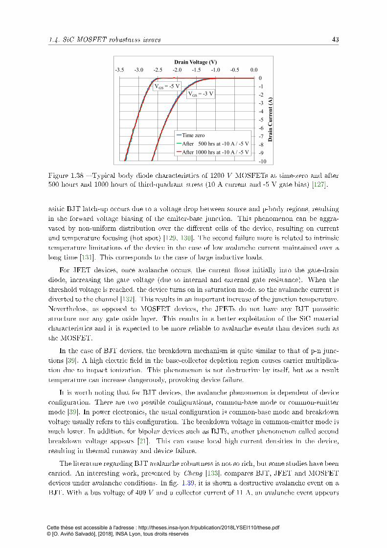
1.4. SiC MOSFET robustness issues 43
-10
-9
-8
-7
-6
-5
-4
-3
-2
-1
0
-3.5 -3.0 -2.5 -2.0 -1.5 -1.0 -0.5 0.0
Dra
in C
urr
ent
(A)
Drain Voltage (V)
Time zero
After 500 hrs at -10 A / -5 V
After 1000 hrs at -10 A / -5 V
VGS = -3 VVGS = -5 V
Figure 1.38 Typical body diode characteristics of 1200 V MOSFETs at time-zero and after500 hours and 1000 hours of third-quadrant stress (10 A current and -5 V gate bias) [127].
asitic BJT latch-up occurs due to a voltage drop between source and p-body regions, resultingin the forward voltage biasing of the emiter-base junction. This phenomenon can be aggra-vated by non-uniform distribution over the dierent cells of the device, resulting on currentand temperature focusing (hot spot) [129, 130]. The second failure more is related to intrinsictemperature limitations of the device in the case of low avalanche current maintained over along time [131]. This corresponds to the case of large inductive loads.
For JFET devices, once avalanche occurs, the current ows initially into the gate-draindiode, increasing the gate voltage (due to internal and external gate resistance). When thethreshold voltage is reached, the device turns on in saturation mode, so the avalanche current isdiverted to the channel [132]. This results in an important increase of the junction temperature.Nevertheless, as opposed to MOSFET devices, the JFETs do not have any BJT parasiticstructure nor any gate oxide layer. This results in a better exploitation of the SiC materialcharacteristics and it is expected to be more reliable to avalanche events than devices such asthe MOSFET.
In the case of BJT devices, the breakdown mechanism is quite similar to that of p-n junc-tions [39]. A high electric eld in the base-collector depletion region causes carrier multiplica-tion due to impact ionization. This phenomenon is not destructive by itself, but as a resulttemperature can increase dangerously, provoking device failure.
It is worth noting that for BJT devices, the avalanche phenomenon is dependent of deviceconguration. There are two possible congurations, common-base mode or common-emittermode [39]. In power electronics, the usual conguration is common-base mode and breakdownvoltage usually refers to this conguration. The breakdown voltage in common-emitter mode ismuch lower. In addition, for bipolar devices such as BJTs, another phenomenon called secondbreakdown voltage appears [21]. This can cause local high-current densities in the device,resulting in thermal runaway and device failure.
The literature regarding BJT avalanche robustness is not so rich, but some studies have beencarried. An interesting work, presented by Cheng [133], compares BJT, JFET and MOSFETdevices under avalanche conditions. In g. 1.39, it is shown a destructive avalanche event on aBJT. With a bus voltage of 400 V and a collector current of 11 A, an avalanche event appears
Cette thèse est accessible à l'adresse : http://theses.insa-lyon.fr/publication/2018LYSEI110/these.pdf © [O. Aviñó Salvadó], [2018], INSA Lyon, tous droits réservés
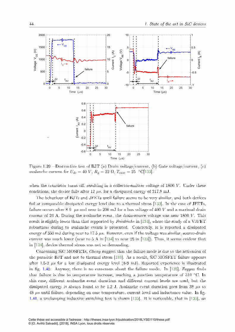
44 1. State of the art in SiC devices
(a) (b)
Figure 1.39 Destructive test of BJT (a) Drain voltage/current, (b) Gate voltage/current, (c)avalanche current for Udc = 40 V , Rg = 22 Ω, Tcase = 25 C[133].
when the transistor turns o, resulting in a collector-emitter voltage of 1800 V . Under theseconditions, the device fails after 12 µs, for a dissipated energy of 217.8 mJ.
The behaviour of BJTs and JFETs until failure seems to be very similar, and both devicesfail at comparable dissipated energy level due to a thermal stress [133]. In the case of JFETs,failure occurs after 8-9 µs and near to 200 mJ for a bus voltage of 400 V and a maximal draincurrent of 24 A. During the avalanche event, the drain-source voltage was near 1800 V . Thisresult is slightly lower than that repported by Friedrichs in [134], where the study of a VJFETrobustness during to avalanche events is presented. Concretely, it is reported a dissipatedenergy of 350 mJ during near to 17.5 µs. However, even if the voltage was similar, source-draincurrent was much lower (near to 5 A in [134] vs near 25 in [133]). Thus, it seems evident thatin [134], device thermal stress was not so demanding.
Concerning SiC MOSFETs, Cheng suggest that the failure mode is due to the activation ofthe parasitic BJT and not to thermal stress [133]. As a result, SiC MOSFET failure appearsafter 1.5-2 µs for a low dissipated energy level (8-9 mJ). Reported experience is illustratedin g. 1.40. Anyway, there is no consensus about the failure mode. In [135], Fayyaz ndsthat failure is due to temperature increase, reaching a junction temperature of 510 C. Inthis case, dierent avalanche event durations and dierent current levels are used, but thedissipated energy is always found to be 1.2 J. Avalanche event duration goes from 38 µs to48 µs until failure, depending on case temperature, current level and inductance value. In g.1.41, a unclamping inductive switching test is shown [135]. It is noticeable, that in [135], an
Cette thèse est accessible à l'adresse : http://theses.insa-lyon.fr/publication/2018LYSEI110/these.pdf © [O. Aviñó Salvadó], [2018], INSA Lyon, tous droits réservés
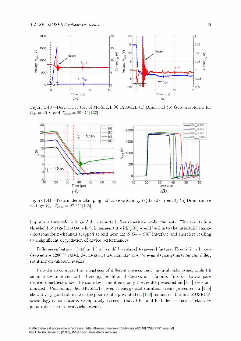
1.4. SiC MOSFET robustness issues 45
(a) (b)
Figure 1.40 Destructive test of MOSFET SCT2080KE (a) Drain and (b) Gate waveforms forUdc = 40 V and Tcase = 25 C [133].
(A) (B)
t2 = 35us
t1 = 28us
Figure 1.41 Tests under unclamping inductive switching. (a) Load current IL (b) Drain-sourcevoltage Vds. Tcase = 27 C [135].
important threshold voltage shift is reported after repetitive avalanche tests. This results in athreshold voltage increase, which in agreement with [135] would be due to the interfacial charge(electrons for n-channel) trapped at and near the SiO2 − SiC interface and therefore leadingto a signicant degradation of device performances.
Dierences between [133] and [135] could be related to several factors. Even if in all casesdevices are 1200 V rated, device structure, manufacturer or even device generation can dier,resulting on dierent results.
In order to compare the robustness of dierent devices under an avalanche event, table 1.6summarizes time and critical energy for dierent devices until failure. In order to comparedevice robustness under the same test conditions, only the results presented on [133] are sum-marized. Concerning SiC MOSFETs, even if energy and duration events presented in [135]show a very good robustness, the poor results presented on [133] remind us that SiC MOSFETstechnology is not mature. Comparably, it seems that JFET and BJT devices have a relativelygood robustness to avalanche events.
Cette thèse est accessible à l'adresse : http://theses.insa-lyon.fr/publication/2018LYSEI110/these.pdf © [O. Aviñó Salvadó], [2018], INSA Lyon, tous droits réservés
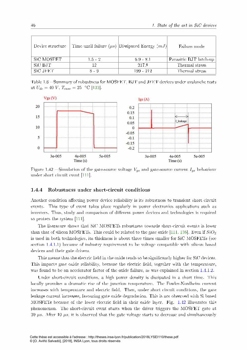
46 1. State of the art in SiC devices
Device structure Time until failure (µs) Dissipated Energy (mJ) Failure mode
SiC MOSFET 1.5 - 2 6.9 - 8.1 Parasitic BJT latch-upSiC BJT 12 217.8 Thermal stressSiC JFET 8 - 9 199 - 212 Thermal stress
Table 1.6 Summary of robustness for MOSFET, BJT and JFET devices under avalanche testsat Udc = 40 V , Tcase = 25 C [133].
Figure 1.42 Simulation of the gate-source voltage Vgs and gate-source current Igs behaviourunder short circuit event [111].
1.4.4 Robustness under short-circuit conditions
Another condition aecting power device reliability is its robustness to transient short circuitevents. This type of event takes place regularly in power electronics applications such asinverters. Thus, study and comparison of dierent power devices and technologies is requiredto protect the system [111].
The literature shows that SiC MOSFETs robustness towards short-circuit events is lowerthan that of silicon MOSFETs. This could be related to the gate oxide [111, 136]. Even if SiO2
is used in both technologies, its thickness is about three times smaller for SiC MOSFETs (seesection 1.4.1.1) because of industry requirement to be voltage compatible with silicon baseddevices and their gate drivers.
This means that the electric eld in the oxide tends to be signicantly higher for SiC devices.This impacts gate oxide reliability, because the electric eld, together with the temperature,was found to be an accelerator factor of the oxide failure, as was explained in section 1.4.1.2.
Under short-circuit conditions, a high power density is dissipated in a short time. Thislocally provokes a dramatic rise of the junction temperature. The Fowler-Nordheim currentincreases with temperature and electric eld. Then, under short-circuit conditions, the gateleakage current increases, favouring gate oxide degradation. This is not observed with Si basedMOSFETs because of the lower electric eld in their oxide layer. Fig. 1.42 illustrates thisphenomenon. The short-circuit event starts when the driver triggers the MOSFET gate at30 µs. After 10 µs, it is observed that the gate voltage starts to decrease and simultaneously
Cette thèse est accessible à l'adresse : http://theses.insa-lyon.fr/publication/2018LYSEI110/these.pdf © [O. Aviñó Salvadó], [2018], INSA Lyon, tous droits réservés
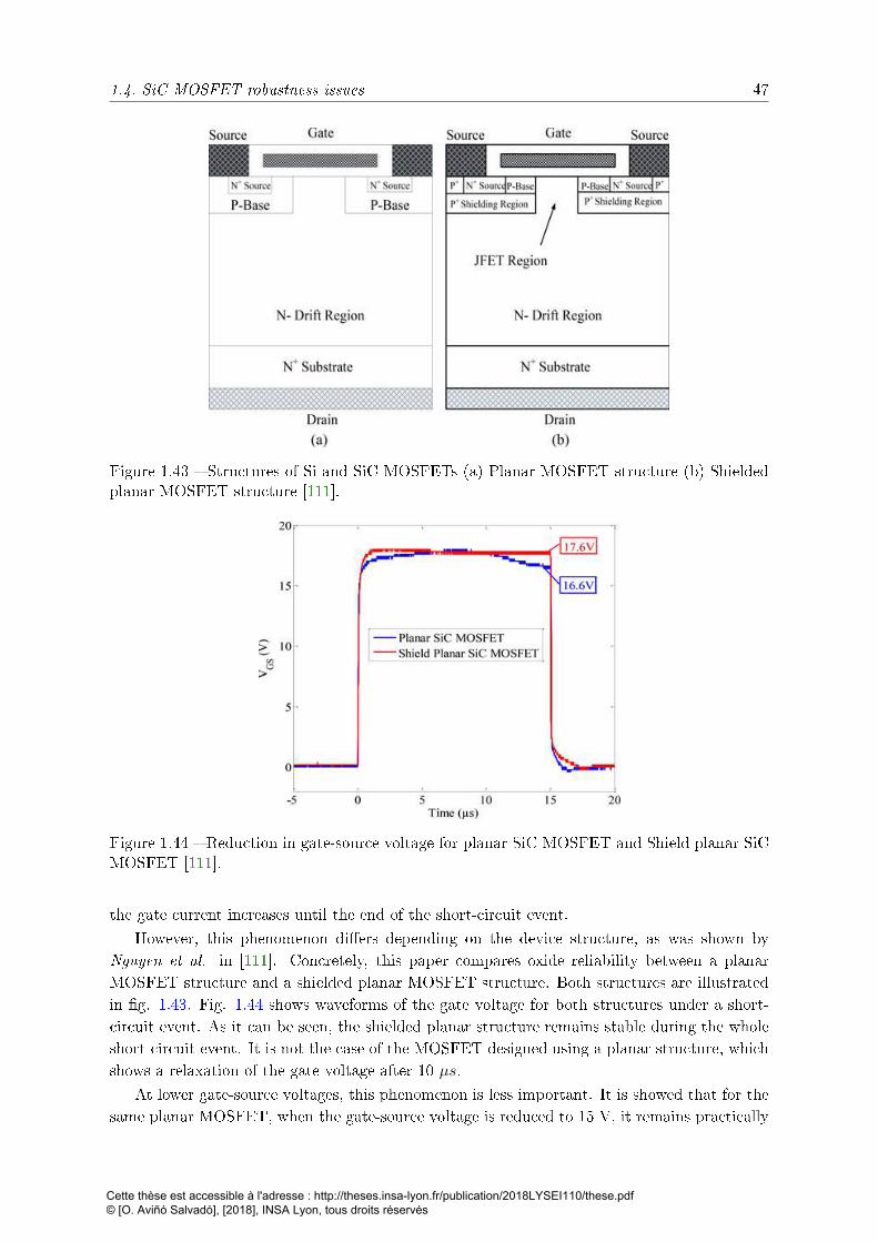
1.4. SiC MOSFET robustness issues 47
Figure 1.43 Structures of Si and SiC MOSFETs (a) Planar MOSFET structure (b) Shieldedplanar MOSFET structure [111].
Figure 1.44 Reduction in gate-source voltage for planar SiC MOSFET and Shield planar SiCMOSFET [111].
the gate current increases until the end of the short-circuit event.
However, this phenomenon diers depending on the device structure, as was shown byNguyen et al. in [111]. Concretely, this paper compares oxide reliability between a planarMOSFET structure and a shielded planar MOSFET structure. Both structures are illustratedin g. 1.43. Fig. 1.44 shows waveforms of the gate voltage for both structures under a short-circuit event. As it can be seen, the shielded planar structure remains stable during the wholeshort-circuit event. It is not the case of the MOSFET designed using a planar structure, whichshows a relaxation of the gate voltage after 10 µs.
At lower gate-source voltages, this phenomenon is less important. It is showed that for thesame planar MOSFET, when the gate-source voltage is reduced to 15 V, it remains practically
Cette thèse est accessible à l'adresse : http://theses.insa-lyon.fr/publication/2018LYSEI110/these.pdf © [O. Aviñó Salvadó], [2018], INSA Lyon, tous droits réservés
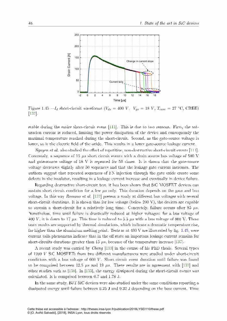
48 1. State of the art in SiC devices
Figure 1.45 Id short-circuit waveforms (Vds = 400 V , Vgs = 18 V , Tcase = 27 C, CREE)[137].
stable during the entire short-circuit event [111]. This is due to two reasons. First, the sat-uration current is reduced, limiting the power dissipation of the device and consequently themaximal temperature reached during the short-circuit. Second, as the gate-source voltage islower, so is the electric eld of the oxide. This results in a lower gate-source leakage current.
Nguyen et al. also studied the eect of repetitive, non-destructive short-circuit events [111].Concretely, a sequence of 15 µs short-circuit events with a drain-source bus voltage of 500 Vand gate-source voltage of 18 V is repeated for 50 times. It is shown that the gate-sourcevoltage decreases slightly after 50 sequences and that the leakage gate current increases. Theauthors suggest that repeated sequences of FN injection through the gate oxide create somedefects in the insulator, resulting in a leakage current increase and eventually in device failure.
Regarding destructive short-circuit test, it has been shown that SiC MOSFET devices cansustain short-circuit condition for a few µs only. This duration depends on the gate and busvoltage. In this way Romano et al. [137] present a study at dierent bus voltages with severalshort-circuit durations. It is shown that for low voltage (below 200 V), the devices are capableto sustain a short-circuit for a relatively long time. Concretely, failure occurs after 85 µs.Nonetheless, time until failure is drastically reduced at higher voltages: for a bus voltage of400 V , it is down to 17 µs. This time is reduced to 5.5 µs with a bus voltage of 800 V. Thesetests results are supported by thermal simulations, which indicate a dramatic temperature rise,far higher than the aluminium melting point. Tests at at 400 V are illustrated by g. 1.45, werecurrent tails phenomena indicate that in the o state an important leakage current remains forshort-circuits durations greater than 15 µs, because of the temperature increase [137].
A recent study was carried by Cheng [133] in the course of his PhD thesis. Several typesof 1200 V SiC MOSFETs from two dierent manufacturers were studied under short-circuitconditions with a bus voltage of 600 V . Short-circuit event duration until failure was foundto be comprised between 12.5 µs and 19 µs. These results are in agreement with [137] andother studies such as [138]. In [133], the energy dissipated during the short-circuit events wascalculated. It is comprised between 0.7 and 1.78 J.
In the same study, BJT SiC devices were also studied under the same conditions reporting adissipated energy until failure between 0.25 J and 0.32 J depending on the base current. Time
Cette thèse est accessible à l'adresse : http://theses.insa-lyon.fr/publication/2018LYSEI110/these.pdf © [O. Aviñó Salvadó], [2018], INSA Lyon, tous droits réservés
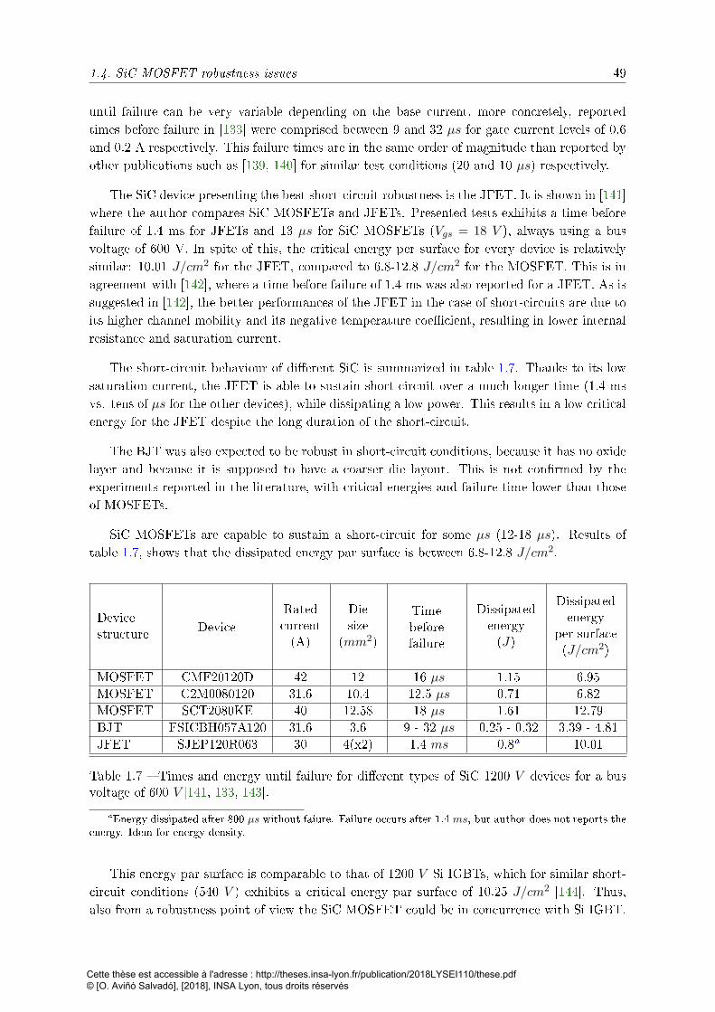
1.4. SiC MOSFET robustness issues 49
until failure can be very variable depending on the base current, more concretely, reportedtimes before failure in [133] were comprised between 9 and 32 µs for gate current levels of 0.6and 0.2 A respectively. This failure times are in the same order of magnitude than reported byother publications such as [139, 140] for similar test conditions (20 and 10 µs) respectively.
The SiC device presenting the best short-circuit robustness is the JFET. It is shown in [141]where the author compares SiC MOSFETs and JFETs. Presented tests exhibits a time beforefailure of 1.4 ms for JFETs and 13 µs for SiC MOSFETs (Vgs = 18 V ), always using a busvoltage of 600 V. In spite of this, the critical energy per surface for every device is relativelysimilar: 10.01 J/cm2 for the JFET, compared to 6.8-12.8 J/cm2 for the MOSFET. This is inagreement with [142], where a time before failure of 1.4 ms was also reported for a JFET. As issuggested in [142], the better performances of the JFET in the case of short-circuits are due toits higher channel mobility and its negative temperature coecient, resulting in lower internalresistance and saturation current.
The short-circuit behaviour of dierent SiC is summarized in table 1.7. Thanks to its lowsaturation current, the JFET is able to sustain short-circuit over a much longer time (1.4 msvs. tens of µs for the other devices), while dissipating a low power. This results in a low criticalenergy for the JFET despite the long duration of the short-circuit.
The BJT was also expected to be robust in short-circuit conditions, because it has no oxidelayer and because it is supposed to have a coarser die layout. This is not conrmed by theexperiments reported in the literature, with critical energies and failure time lower than thoseof MOSFETs.
SiC MOSFETs are capable to sustain a short-circuit for some µs (12-18 µs). Results oftable 1.7, shows that the dissipated energy par surface is between 6.8-12.8 J/cm2.
Devicestructure Device
Ratedcurrent(A)
Diesize
(mm2)
Timebeforefailure
Dissipatedenergy(J)
Dissipatedenergy
per surface(J/cm2)
MOSFET CMF20120D 42 12 16 µs 1.15 6.95MOSFET C2M0080120 31.6 10.4 12.5 µs 0.71 6.82MOSFET SCT2080KE 40 12.58 18 µs 1.61 12.79BJT FSICBH057A120 31.6 3.6 9 - 32 µs 0.25 - 0.32 3.39 - 4.81JFET SJEP120R063 30 4(x2) 1.4 ms 0.8a 10.01
Table 1.7 Times and energy until failure for dierent types of SiC 1200 V devices for a busvoltage of 600 V [141, 133, 143].
aEnergy dissipated after 800 µs without faiure. Failure occurs after 1.4 ms, but author does not reports theenergy. Idem for energy density.
This energy par surface is comparable to that of 1200 V Si IGBTs, which for similar short-circuit conditions (540 V ) exhibits a critical energy par surface of 10.25 J/cm2 [144]. Thus,also from a robustness point of view the SiC MOSFET could be in concurrence with Si IGBT.
Cette thèse est accessible à l'adresse : http://theses.insa-lyon.fr/publication/2018LYSEI110/these.pdf © [O. Aviñó Salvadó], [2018], INSA Lyon, tous droits réservés
50 1. State of the art in SiC devices
1.5 Conclusions
In this chapter the main properties of SiC were presented and compared to those of Si (seesection 1.1). As a result, we highlighted the advantages of SiC for power devices. However,SiC substrates still show some reliability issues related to crystallographic defects, as relatedin section 1.2. These defects have been delaying SiC power devices development for long time,restricting it to academic research. Recently, most of these issues have been overcome, andmany academic studies now focus on evaluating the performance of SiC power device structures.These structures are presented in section 1.3, and they are BJT, JFET, MOSFET and IGBT.
Among these devices, BJTs and JFETs present some drawbacks for the industry. The rstone is a current controlled device, while the second is a normally-on device. These characteristicsare in opposition with industry standards, which prefer devices with high input impedance(voltage controlled) and which remain in the o state in the case of driver failure. As a result,the MOSFET is the most attractive device structure, and seem to be the alternative beingconsidered by the industry for applications below 10 kV. SiC IGBTs would be an alternativeonly for higher voltages, but they are currently under development, and no commercializationis expected in the short term.
However, the manufacturing process of SiC MOSFETs is complex, and some reliabilityissues remain. They are presented in section 1.4, and are related to the gate oxide, the intrinsicdiode and to the behaviour under avalanche and short-circuit conditions. Short-circuit andavalanche phenomena are common reliability issues of all the presented devices. A brief stateof the art regarding these devices has been presented.
This thesis will focus on two intrinsic reliability issues of the SiC MOSFET: intrinsic diodedegradation and the reliability of the gate oxide. They are presented in chapters 2 and 3respectively.
Cette thèse est accessible à l'adresse : http://theses.insa-lyon.fr/publication/2018LYSEI110/these.pdf © [O. Aviñó Salvadó], [2018], INSA Lyon, tous droits réservés
Chapter 2
Robustness of the MOSFET internal diode
Contents
2.1 Introduction . . . . . . . . . . . . . . . . . . . . . . . . . . . . . . . . 51
2.2 Context . . . . . . . . . . . . . . . . . . . . . . . . . . . . . . . . . . . . 52
2.3 Static tests . . . . . . . . . . . . . . . . . . . . . . . . . . . . . . . . . . 54
2.3.1 Description of the set-ups for static tests . . . . . . . . . . . . . . . . 54
2.3.2 Experimental Results . . . . . . . . . . . . . . . . . . . . . . . . . . . 59
2.3.3 Discussion . . . . . . . . . . . . . . . . . . . . . . . . . . . . . . . . . 65
2.4 Testing SiC MOSFET internal-diode for an induc-
tive switching application . . . . . . . . . . . . . . . . . . . . . . 67
2.4.1 Test-bench description . . . . . . . . . . . . . . . . . . . . . . . . . . 67
2.4.2 Experimental Results . . . . . . . . . . . . . . . . . . . . . . . . . . . 73
2.4.3 Discussion . . . . . . . . . . . . . . . . . . . . . . . . . . . . . . . . . 78
2.5 Conclusions . . . . . . . . . . . . . . . . . . . . . . . . . . . . . . . . . 80
2.1 Introduction
SiC devices are especially attractive for power applications. For example, replacing Si IGBTswith SiC MOSFETs, allows important loss reduction, which, associated with better thermaland frequency performances, may yield to a reduction of the system dimensions.
However attractive the material is, the commercial development of SiC devices faces tech-nological challenges about defect elimination. Among them, dislocation issues and micropipeshave limited for a long time the forward-blocking capacity of SiC devices at high voltages,one of SiC most promising applications. Besides, the electron mobility in the SiC MOSFETschannel is limited because of the presence of crystal defects and interface states.
Although manufacturers have considerably minimised these defects for the last commer-cialised SiC devices, these are not fully controlled yet and some reliability problems remain, aspresented in chapter 1. Among these issues, there is the degradation of the internal diode.
In this chapter, the robustness of the internal diode of SiC MOSFETs is assessed understatic, but also under realistic (switching) operating conditions. This work is oriented towardsaeronautical applications (inductive switching and a bus voltage of 540 V, corresponding tothe future aircraft HVDC network). The objective is to study whether current commercial SiCMOSFET devices could be used in diode-less applications.
An example of such application is an inverter where the transistors are mounted withoutantiparallel diodes. Diode-less converters require fewer components and may reduce losses,hence a more compact,ecient and cheaper system. In such conditions, [145] reported a drift
Cette thèse est accessible à l'adresse : http://theses.insa-lyon.fr/publication/2018LYSEI110/these.pdf © [O. Aviñó Salvadó], [2018], INSA Lyon, tous droits réservés
52 2. Robustness of the MOSFET internal diode
Figure 2.1 Typical forward current-voltage characteristics of pn-junction-based body diodein a conventional SiC MOSFET after applying forward current of 15 A [145] (2016).
in the voltage threshold of some MOSFETs. We also monitor this parameter, which is especiallyimportant, as it has consequences on the gate drive circuit design.
To evaluate the robustness of the internal diode of SiC MOSFETs, some tests are presentedin this chapter. Firstly, several static test stressing the internal diode are realized, with regularMOSFET characterizations to evaluate possible degradations.
Secondly, we focus on a more realistic case. The MOSFETs are placed in a real converter,with inductive switching conditions, a bus voltage of 540 V and at their maximal operationtemperature. The inuence of MOSFET switching and operation duty cycle is analysed.
2.2 Context
As it has been presented in chapter 1, MOSFET internal diode stresses could result in twoprincipal reliability issues. The rst one, an increase in the diode forward voltage, increasinglosses. The second is a shift in the voltage threshold of the MOSFET. This could result in moreresistive devices due to a voltage threshold increase. In this case, thermal runaway could be theprincipal risk. In the case of a negative voltage threshold shift, the MOSFET could become anormally-on device or simply more sensitive to EMI (Electromagnetic interference). In eithercase, it might cause dramatic failures.
A commonly used solution to avoid any P-N junction degradation is to use a Schottky diodein an antiparallel conguration. This solution also oers advantages such as faster recoverytime and perhaps lower losses. However, it has the downside of requiring more components.An intermediate solution is a structure integrating a Shottky diode in the MOSFET die [146,145].
When no schottky diode is used, Kusumoto et al. showed [145] a forward voltage shift inthe case of an internal diode stress at 15 A. This is illustrated by g. 2.1, where there areno changes in the built-in voltage Vbi, but in the series dynamic resistance; probably due to adegradation of the source metallization. In addition, a threshold voltage drift of the channelwas also observed in two dierent cases (both at 150 C): the rst one, for a gate bias of 20 V ,and the second one at Vgs =-10 V . These two cases are illustrated in g. 2.2. Finally, it was
Cette thèse est accessible à l'adresse : http://theses.insa-lyon.fr/publication/2018LYSEI110/these.pdf © [O. Aviñó Salvadó], [2018], INSA Lyon, tous droits réservés
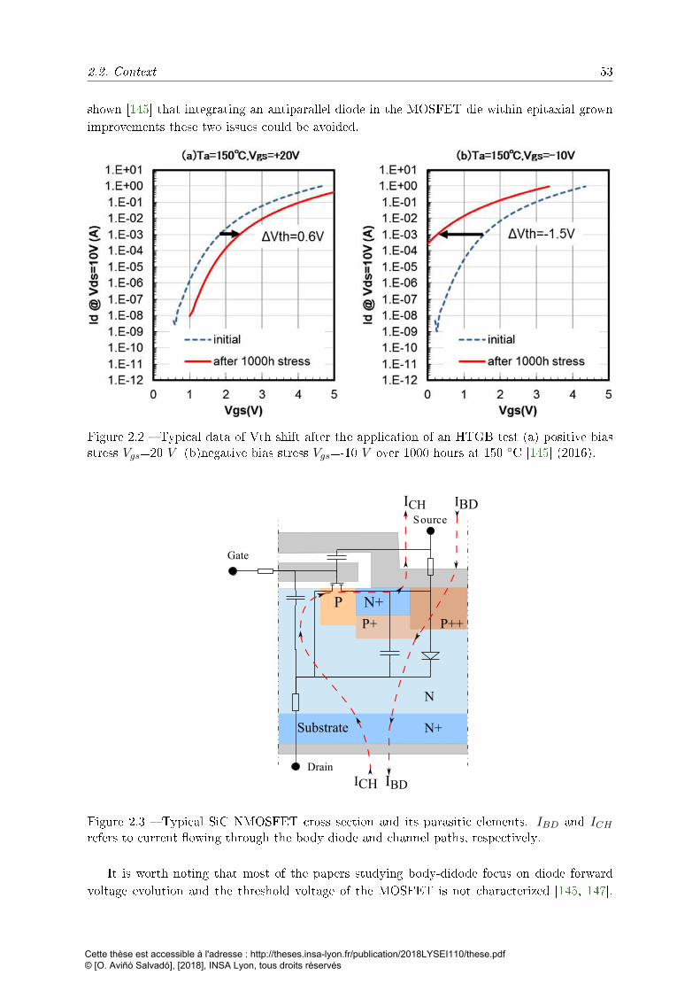
2.2. Context 53
shown [145] that integrating an antiparallel diode in the MOSFET die within epitaxial grownimprovements these two issues could be avoided.
Figure 2.2 Typical data of Vth shift after the application of an HTGB test (a) positive biasstress Vgs=20 V (b)negative bias stress Vgs=-10 V over 1000 hours at 150 C [145] (2016).
Gate
P N+
P++
Substrate N+
IBDICH
IBD ICHSource
Drain
N
P+
Figure 2.3 Typical SiC NMOSFET cross section and its parasitic elements. IBD and ICHrefers to current owing through the body diode and channel paths, respectively.
It is worth noting that most of the papers studying body-didode focus on diode forwardvoltage evolution and the threshold voltage of the MOSFET is not characterized [145, 147].
Cette thèse est accessible à l'adresse : http://theses.insa-lyon.fr/publication/2018LYSEI110/these.pdf © [O. Aviñó Salvadó], [2018], INSA Lyon, tous droits réservés
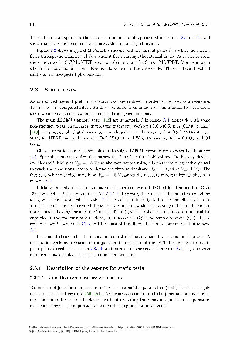
54 2. Robustness of the MOSFET internal diode
Thus, this issue requires further investigation and results presented in sections 2.3 and 2.4 willshow that body-diode stress may cause a shift in voltage threshold.
Figure 2.3 shows a typical MOSFET structure and the current paths ICH when the currentows through the channel and IBD when it ows through the internal diode. As it can be seen,the structure of a SiC MOSFET is comparable to that of a Silicon MOSFET. Moreover, as insilicon the body diode current does not ows near to the gate oxide. Thus, voltage thresholdshift was an unexpected phenomenon.
2.3 Static tests
As introduced, several preliminary static test are realized in order to be used as a reference.The results are compared later with those obtained from inductive commutation tests, in orderto draw some conclusions about the degradation phenomenons.
The main JEDEC standard tests [148] are summarized in annex A.1 alongside with somenon-standard tests. In all cases, devices under test are Wolfspeed SiC MOSFETs (C2M008012D)[149]. It is noticeable that devices were purchased in two batches: a rst (Ref. W14514, year2014) for HTGB test and a second (Ref. W10116 and W10216, year 2016) for Q1,Q3 and Q4tests.
Characterizations are realized using an Keysight B1505B curve tracer as described in annexA.2. Special attention requires the characterisation of the threshold voltage. In this way, devicesare blocked initially at Vgs = −8 V and the gate-source voltage is increased progressively untilto reach the conditions chosen to dene the threshold voltage (Ids=100 µA at Vds=1 V ). Thefact to block the device initially at Vgs = −8 V assures the measure repeatability, as shown inannexe A.2.
Initially, the only static test we intended to perform was a HTGB (High Temperature GateBias) test, which is presented in section 2.3.1.2. However, the results of the inductive switchingtests, which are presented in section 2.4, forced us to investigate further the eects of staticstresses. Thus, three dierent static tests are run. One with a negative gate bias and a sourcedrain current owing through the internal diode (Q3); the other two tests are run at positivegate bias in the two current directions, drain to source (Q1) and source to drain (Q4). Theseare described in section 2.3.1.3. All the data of the dierent tests are summarized in annexeA.6.
In some of these tests, the device under test dissipates a signicant amount of power. Amethod is developed to estimate the junction temperature of the DUT during these tests. Itsprinciple is described in section 2.3.1.1, and more details are given in annexe A.4, together withan uncertainty calculation of the junction temperature.
2.3.1 Description of the set-ups for static tests
2.3.1.1 Junction temperature estimation
Estimation of junction temperature using thermosensitive parameters (TSP) has been largelydiscussed in the litterature [150, 151]. An accurate estimation of the junction temperature isimportant in order to test the devices without exceeding their maximal junction temperature,as it could trigger the apparition of some other degradation mechanism.
Cette thèse est accessible à l'adresse : http://theses.insa-lyon.fr/publication/2018LYSEI110/these.pdf © [O. Aviñó Salvadó], [2018], INSA Lyon, tous droits réservés
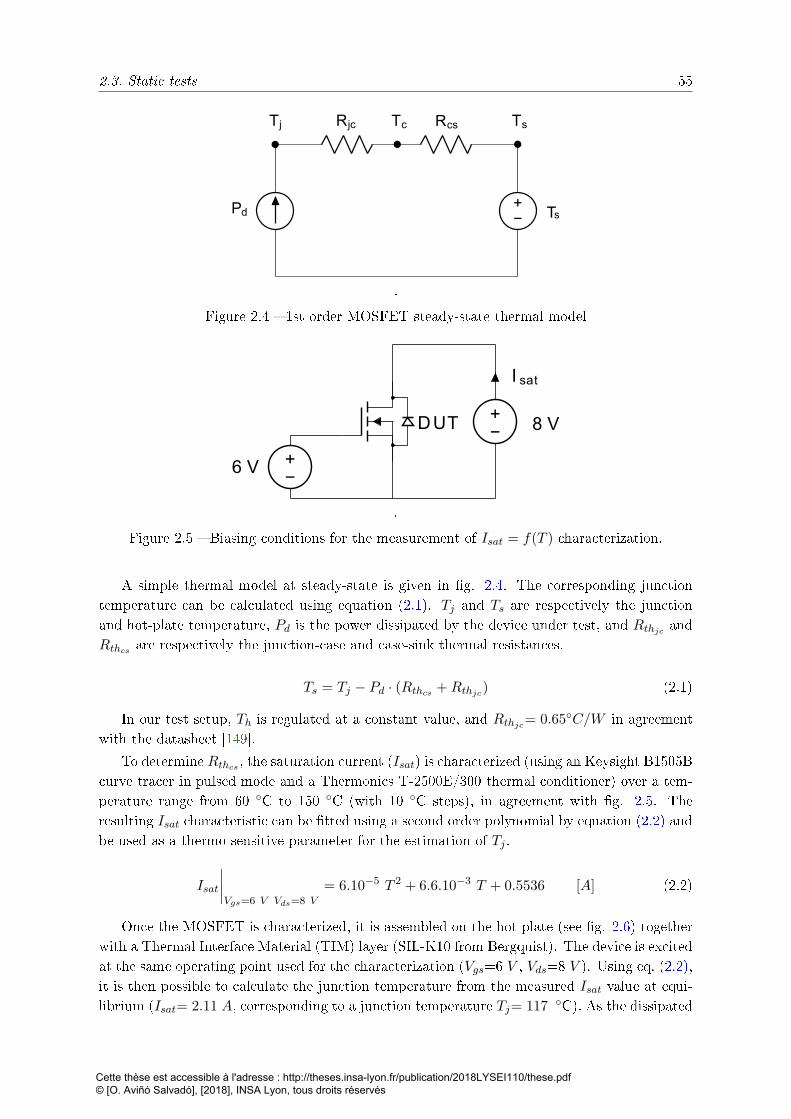
2.3. Static tests 55
Pd
Rjc Rcs
−+
Ts
Tj Tc Ts
.
Figure 2.4 1st order MOSFET steady-state thermal model
DUT
−+6 V
−+ 8 V
I sat
.
Figure 2.5 Biasing conditions for the measurement of Isat = f(T ) characterization.
A simple thermal model at steady-state is given in g. 2.4. The corresponding junctiontemperature can be calculated using equation (2.1). Tj and Ts are respectively the junctionand hot-plate temperature, Pd is the power dissipated by the device under test, and Rthjc andRthcs are respectively the junction-case and case-sink thermal resistances.
Ts = Tj − Pd · (Rthcs +Rthjc) (2.1)
In our test setup, Th is regulated at a constant value, and Rthjc= 0.65C/W in agreementwith the datasheet [149].
To determine Rthcs , the saturation current (Isat) is characterized (using an Keysight B1505Bcurve tracer in pulsed mode and a Thermonics T-2500E/300 thermal conditioner) over a tem-perature range from 60 C to 150 C (with 10 C steps), in agreement with g. 2.5. Theresulting Isat characteristic can be tted using a second order polynomial by equation (2.2) andbe used as a thermo-sensitive parameter for the estimation of Tj .
Isat
∣∣∣∣Vgs=6 V Vds=8 V
= 6.10−5 T 2 + 6.6.10−3 T + 0.5536 [A] (2.2)
Once the MOSFET is characterized, it is assembled on the hot plate (see g. 2.6) togetherwith a Thermal Interface Material (TIM) layer (SIL-K10 from Bergquist). The device is excitedat the same operating point used for the characterization (Vgs=6 V , Vds=8 V ). Using eq. (2.2),it is then possible to calculate the junction temperature from the measured Isat value at equi-librium (Isat= 2.11 A, corresponding to a junction temperature Tj= 117 C). As the dissipated
Cette thèse est accessible à l'adresse : http://theses.insa-lyon.fr/publication/2018LYSEI110/these.pdf © [O. Aviñó Salvadó], [2018], INSA Lyon, tous droits réservés
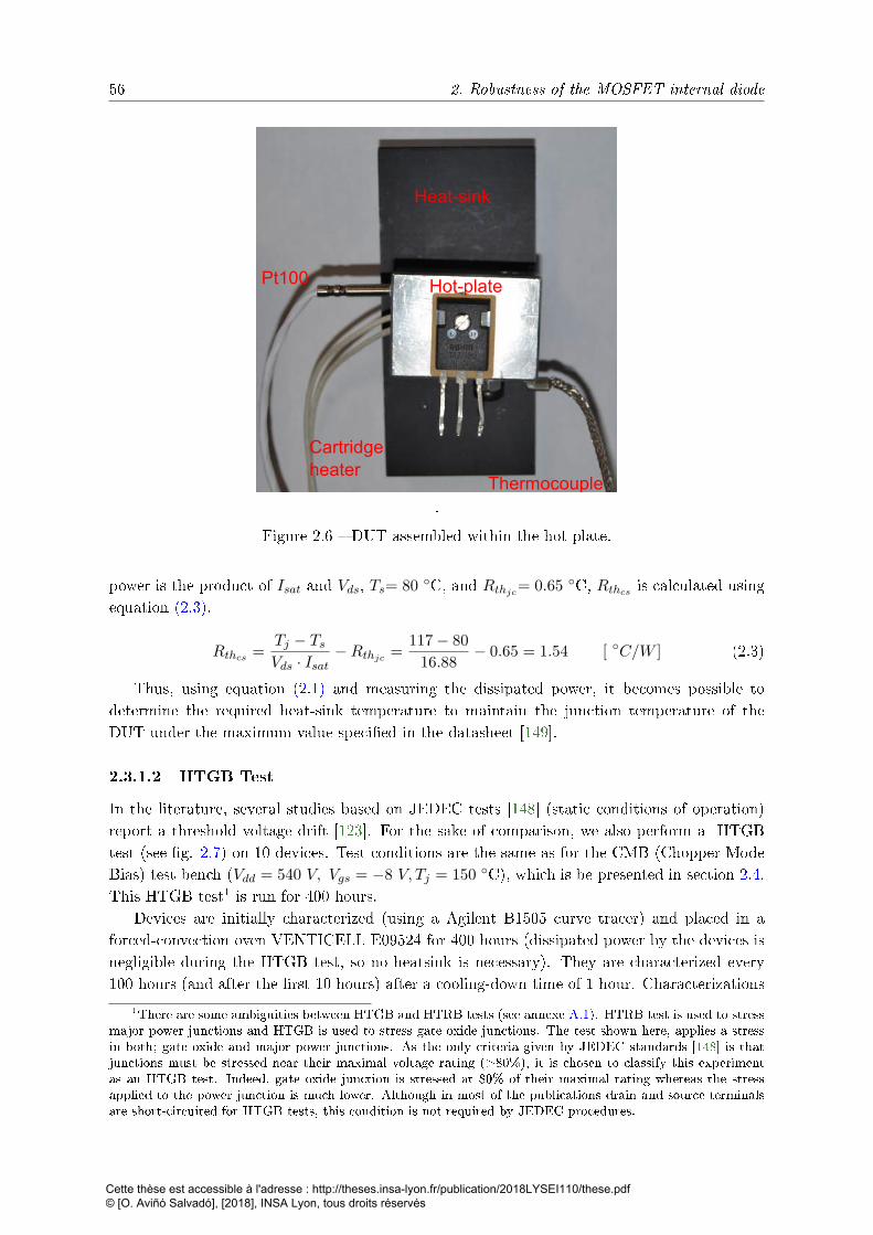
56 2. Robustness of the MOSFET internal diode
Pt100
Cartridgeheater
Thermocouple
Heat-sink
Hot-plate
.
Figure 2.6 DUT assembled within the hot-plate.
power is the product of Isat and Vds, Ts= 80 C, and Rthjc= 0.65 C, Rthcs is calculated usingequation (2.3).
Rthcs =Tj − TsVds · Isat
−Rthjc =117− 80
16.88− 0.65 = 1.54 [ C/W ] (2.3)
Thus, using equation (2.1) and measuring the dissipated power, it becomes possible todetermine the required heat-sink temperature to maintain the junction temperature of theDUT under the maximum value specied in the datasheet [149].
2.3.1.2 HTGB Test
In the literature, several studies based on JEDEC tests [148] (static conditions of operation)report a threshold voltage drift [123]. For the sake of comparison, we also perform a HTGBtest (see g. 2.7) on 10 devices. Test conditions are the same as for the CMB (Chopper ModeBias) test bench (Vdd = 540 V, Vgs = −8 V, Tj = 150 C), which is be presented in section 2.4.This HTGB test1 is run for 400 hours.
Devices are initially characterized (using a Agilent B1505 curve tracer) and placed in aforced-convection oven VENTICELL E09524 for 400 hours (dissipated power by the devices isnegligible during the HTGB test, so no heatsink is necessary). They are characterized every100 hours (and after the rst 10 hours) after a cooling-down time of 1 hour. Characterizations
1There are some ambiguities between HTGB and HTRB tests (see annexe A.1). HTRB test is used to stressmajor power junctions and HTGB is used to stress gate oxide junctions. The test shown here, applies a stressin both; gate oxide and major power junctions. As the only criteria given by JEDEC standards [148] is thatjunctions must be stressed near their maximal voltage rating (>80%), it is chosen to classify this experimentas an HTGB test. Indeed, gate oxide junction is stressed at 80% of their maximal rating whereas the stressapplied to the power junction is much lower. Although in most of the publications drain and source terminalsare short-circuited for HTGB tests, this condition is not required by JEDEC procedures.
Cette thèse est accessible à l'adresse : http://theses.insa-lyon.fr/publication/2018LYSEI110/these.pdf © [O. Aviñó Salvadó], [2018], INSA Lyon, tous droits réservés
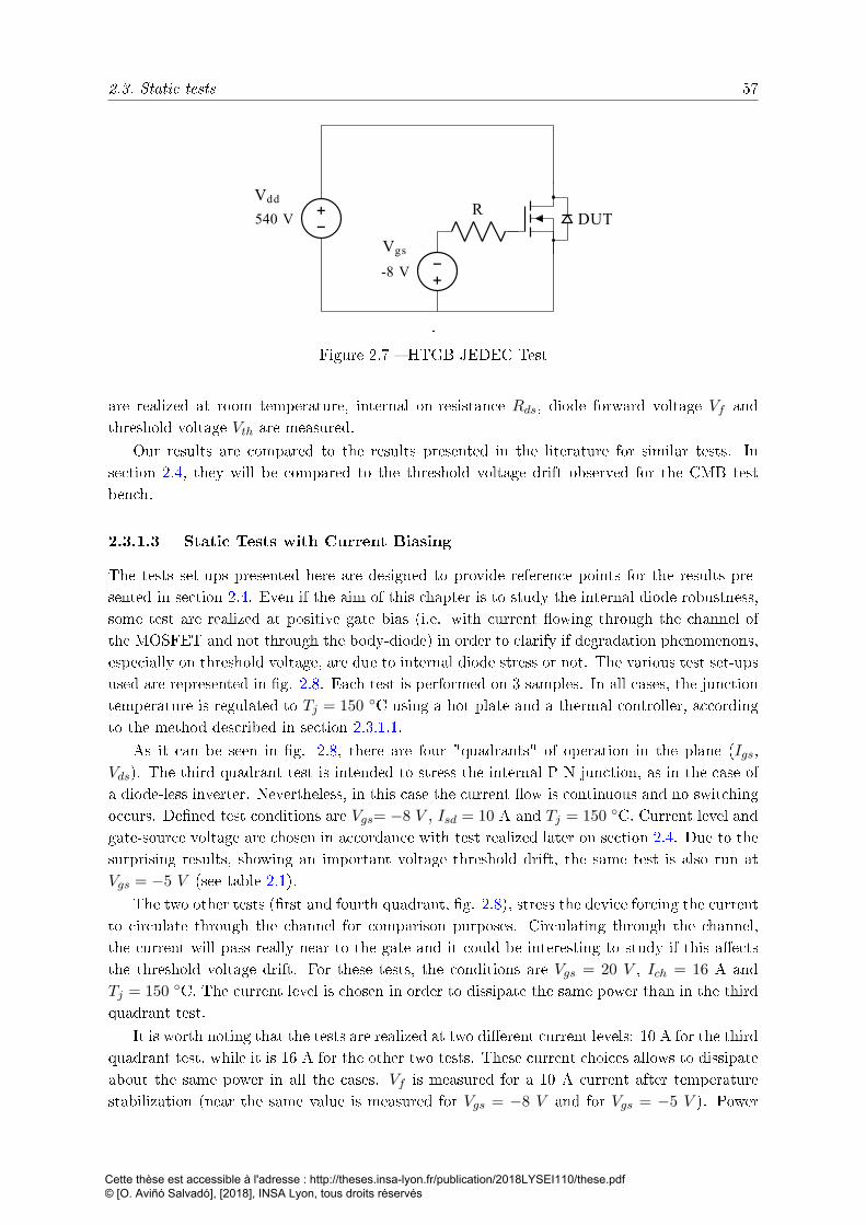
2.3. Static tests 57
−+540 V
Vdd
DUT
−+-8 V
Vgs
R
.
Figure 2.7 HTGB JEDEC Test
are realized at room temperature, internal on-resistance Rds, diode forward voltage Vf andthreshold voltage Vth are measured.
Our results are compared to the results presented in the literature for similar tests. Insection 2.4, they will be compared to the threshold voltage drift observed for the CMB testbench.
2.3.1.3 Static Tests with Current Biasing
The tests set-ups presented here are designed to provide reference points for the results pre-sented in section 2.4. Even if the aim of this chapter is to study the internal diode robustness,some test are realized at positive gate bias (i.e. with current owing through the channel ofthe MOSFET and not through the body-diode) in order to clarify if degradation phenomenons,especially on threshold voltage, are due to internal diode stress or not. The various test set-upsused are represented in g. 2.8. Each test is performed on 3 samples. In all cases, the junctiontemperature is regulated to Tj = 150 C using a hot plate and a thermal controller, accordingto the method described in section 2.3.1.1.
As it can be seen in g. 2.8, there are four "quadrants" of operation in the plane (Igs,Vds). The third quadrant test is intended to stress the internal P-N junction, as in the case ofa diode-less inverter. Nevertheless, in this case the current ow is continuous and no switchingoccurs. Dened test conditions are Vgs= −8 V , Isd = 10 A and Tj = 150 C. Current level andgate-source voltage are chosen in accordance with test realized later on section 2.4. Due to thesurprising results, showing an important voltage threshold drift, the same test is also run atVgs = −5 V (see table 2.1).
The two other tests (rst and fourth quadrant, g. 2.8), stress the device forcing the currentto circulate through the channel for comparison purposes. Circulating through the channel,the current will pass really near to the gate and it could be interesting to study if this aectsthe threshold voltage drift. For these tests, the conditions are Vgs = 20 V , Ich = 16 A andTj = 150 C. The current level is chosen in order to dissipate the same power than in the thirdquadrant test.
It is worth noting that the tests are realized at two dierent current levels: 10 A for the thirdquadrant test, while it is 16 A for the other two tests. These current choices allows to dissipateabout the same power in all the cases. Vf is measured for a 10 A current after temperaturestabilization (near the same value is measured for Vgs = −8 V and for Vgs = −5 V ). Power
Cette thèse est accessible à l'adresse : http://theses.insa-lyon.fr/publication/2018LYSEI110/these.pdf © [O. Aviñó Salvadó], [2018], INSA Lyon, tous droits réservés
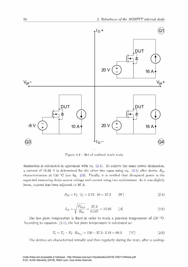
58 2. Robustness of the MOSFET internal diode
DUT
−+20 V 16 A
DUT
−+20 V 16 A
DUT
−+-8 V 10 A
Q1
Q3 Q4
Vgs+Vgs−
I D +
I D −
.
Figure 2.8 Set of realized static tests
dissipation is calculated in agreement with eq. (2.4). To achieve the same power dissipation,a current of 15.93 A is determined for the other two cases using eq. (2.5) after device Rdscharacterisation at 150 C (see g. 2.9). Finally, it is veried that dissipated power is theexpected measuring drain-source voltage and current using two multimeters. As it was slightlylower, current has been adjusted to 16 A.
Pd3 = Vf · If = 3.73 · 10 = 37.3 [W ] (2.4)
Ich =
√Pd1|4
Rds=
37.3
0.147= 15.93 [A] (2.5)
The hot plate temperature is xed in order to reach a junction temperature of 150 C.According to equation. (2.1), the hot plate temperature is calculated as:
Ts = Tj − Pd ·Rthjs = 150− 37.3 · 2.19 = 68.3 [C] (2.6)
The devices are characterized initially and then regularly during the tests, after a cooling-
Cette thèse est accessible à l'adresse : http://theses.insa-lyon.fr/publication/2018LYSEI110/these.pdf © [O. Aviñó Salvadó], [2018], INSA Lyon, tous droits réservés
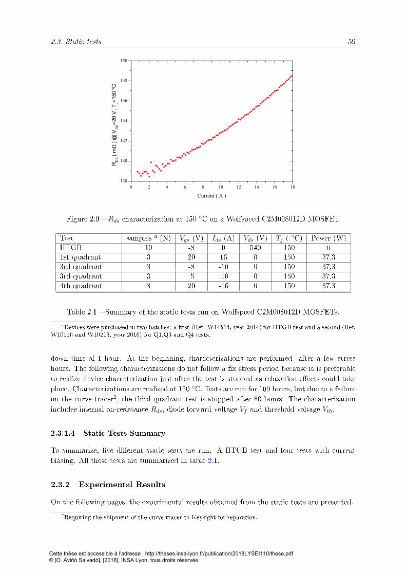
2.3. Static tests 59
0 2 4 6 8 10 12 14 16 18138
140
142
144
146
148
150
RD
S(
mΩ
)@
VG
S=
20 V
, TJ=
150
ºC
Current ( A )
.
Figure 2.9 Rds characterization at 150 C on a Wolfspeed C2M008012D MOSFET
Test samples a (N) Vgs (V) Ids (A) Vds (V) Tj ( C) Power (W)HTGB 10 -8 0 540 150 01st quadrant 3 20 16 0 150 37.33rd quadrant 3 -8 -10 0 150 37.33rd quadrant 3 -5 -10 0 150 37.34th quadrant 3 20 -16 0 150 37.3
Table 2.1 Summary of the static tests run on Wolfspeed C2M008012D MOSFETs.
aDevices were purchased in two batches: a rst (Ref. W14514, year 2014) for HTGB test and a second (Ref.W10116 and W10216, year 2016) for Q1,Q3 and Q4 tests.
down time of 1 hour. At the beginning, characterizations are performed after a few stresshours. The following characterizations do not follow a x stress period because it is preferableto realize device characterization just after the test is stopped as relaxation eects could takeplace. Characterizations are realized at 150 C. Tests are run for 100 hours, but due to a failureon the curve tracer2, the third quadrant test is stopped after 80 hours. The characterizationincludes internal on-resistance Rds, diode forward voltage Vf and threshold voltage Vth.
2.3.1.4 Static Tests Summary
To summarize, ve dierent static tests are run. A HTGB test and four tests with currentbiasing. All these tests are summarized in table 2.1.
2.3.2 Experimental Results
On the following pages, the experimental results obtained from the static tests are presented.
2Requiring the shipment of the curve tracer to Keysight for reparation.
Cette thèse est accessible à l'adresse : http://theses.insa-lyon.fr/publication/2018LYSEI110/these.pdf © [O. Aviñó Salvadó], [2018], INSA Lyon, tous droits réservés

60 2. Robustness of the MOSFET internal diode
0 100 200 300 40095
100
105
110
115
120
125
130
RD
S(
mΩ
)
Stress time ( h )
(a) Rds-on resistance
0 100 200 300 4000.95
1.00
1.05
1.10
1.15
1.20
1.25
Nor
mal
ized
RD
S
Stress time ( h )
(b) Normalized Rds-on resistance
Figure 2.10 Rds-on evolution for HTGB test. Characterised at room temperature,Ids = 10 A and Vgs = 20 V .
0 100 200 300 4004.3
4.4
4.5
4.6
4.7
4.8
4.9
5.0
VF
( V
)
Stress time ( h )
(a) Diode forward voltage
0 100 200 300 400
0.98
1.00
1.02
1.04
Nor
mal
ized
VF
Stress time ( h )
(b) Normalized diode forward voltage
Figure 2.11 Intrinsic diode forward voltage evolution for HTGB test. Characterised at roomtemperature, If = 10 A and Vgs = −8 V .
2.3.2.1 HTGB Test
The HTGB test (Vdd = 540 V, Vgs = −8 V, Tj = 150 C) shown in g. 2.7 is performedon 10 devices. As mentioned earlier, characterized parameters are internal on-resistance Rds,diode forward voltage Vf and threshold voltage Vth. The evolution of these parameters over400 hours is given in gures 2.10 to 2.12. In all cases, the measured and normalized parametervalues are represented. Normalized value is dened as the relation between the measured valueat any given time (ti) and its initial value (at t0) (before starting the test):
Normalized parameter(ti) =Measured parameter(ti)
Measured parameter(t0)(2.7)
Fig. 2.10 shows the evolution of the internal on-resistance over the test at Vgs = 20 V andIds = 10 A. This shows an upward trend of the resistance, increasing by around 15% (≈15 mΩ)after 400 hours. However, it is unclear if this evolution should be attributed to the SiC dieor to its packaging. In our test setup, a 4-wire connexion is used on most of the cabling, but
Cette thèse est accessible à l'adresse : http://theses.insa-lyon.fr/publication/2018LYSEI110/these.pdf © [O. Aviñó Salvadó], [2018], INSA Lyon, tous droits réservés
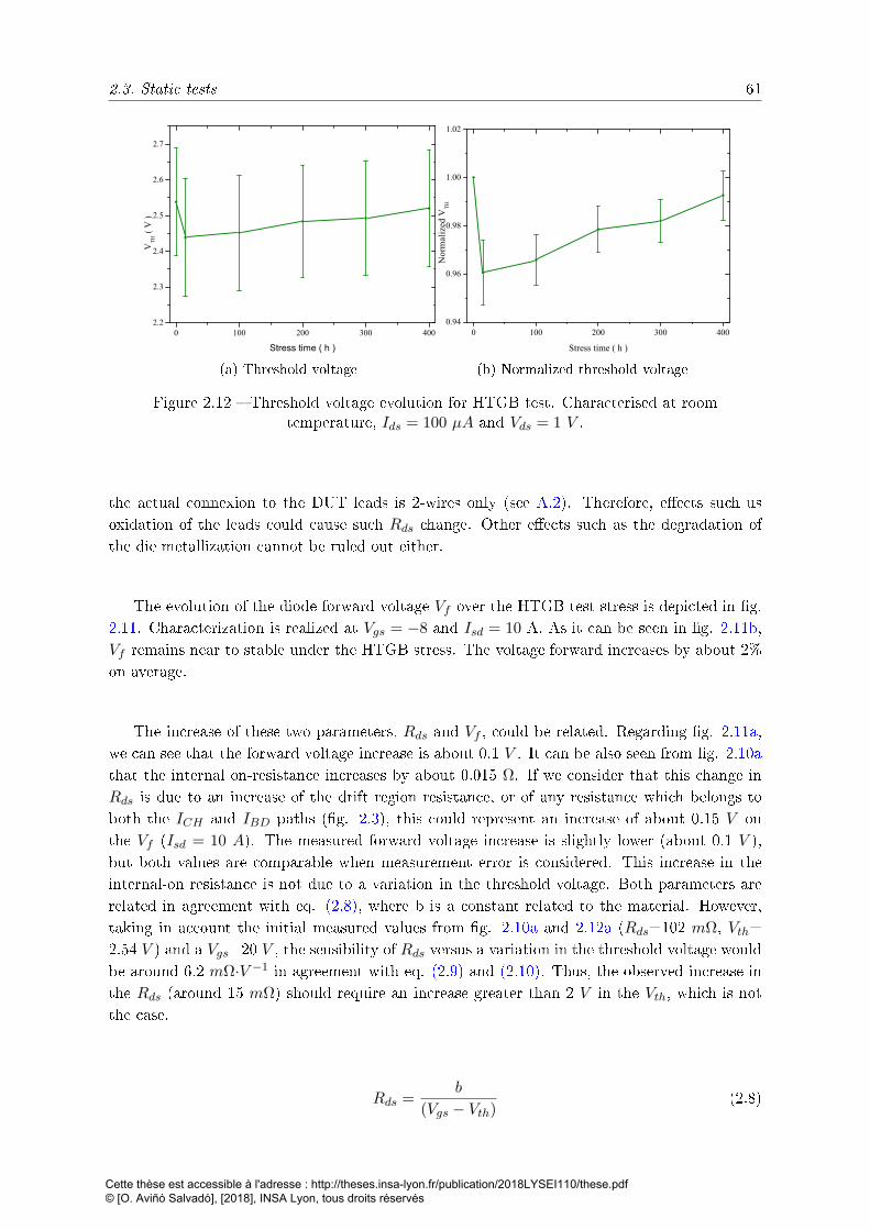
2.3. Static tests 61
0 100 200 300 4002.2
2.3
2.4
2.5
2.6
2.7V
TH
( V
)
Stress time ( h )
(a) Threshold voltage
0 100 200 300 4000.94
0.96
0.98
1.00
1.02
Nor
mal
ized
VT
H
Stress time ( h )
(b) Normalized threshold voltage
Figure 2.12 Threshold voltage evolution for HTGB test. Characterised at roomtemperature, Ids = 100 µA and Vds = 1 V .
the actual connexion to the DUT leads is 2-wires only (see A.2). Therefore, eects such usoxidation of the leads could cause such Rds change. Other eects such as the degradation ofthe die metallization cannot be ruled out either.
The evolution of the diode forward voltage Vf over the HTGB test stress is depicted in g.2.11. Characterization is realized at Vgs = −8 and Isd = 10 A. As it can be seen in g. 2.11b,Vf remains near to stable under the HTGB stress. The voltage forward increases by about 2%on average.
The increase of these two parameters, Rds and Vf , could be related. Regarding g. 2.11a,we can see that the forward voltage increase is about 0.1 V . It can be also seen from g. 2.10athat the internal on-resistance increases by about 0.015 Ω. If we consider that this change inRds is due to an increase of the drift region resistance, or of any resistance which belongs toboth the ICH and IBD paths (g. 2.3), this could represent an increase of about 0.15 V onthe Vf (Isd = 10 A). The measured forward voltage increase is slightly lower (about 0.1 V ),but both values are comparable when measurement error is considered. This increase in theinternal-on resistance is not due to a variation in the threshold voltage. Both parameters arerelated in agreement with eq. (2.8), where b is a constant related to the material. However,taking in account the initial measured values from g. 2.10a and 2.12a (Rds=102 mΩ, Vth=2.54 V ) and a Vgs=20 V , the sensibility of Rds versus a variation in the threshold voltage wouldbe around 6.2 mΩ·V −1 in agreement with eq. (2.9) and (2.10). Thus, the observed increase inthe Rds (around 15 mΩ) should require an increase greater than 2 V in the Vth, which is notthe case.
Rds =b
(Vgs − Vth)(2.8)
Cette thèse est accessible à l'adresse : http://theses.insa-lyon.fr/publication/2018LYSEI110/these.pdf © [O. Aviñó Salvadó], [2018], INSA Lyon, tous droits réservés
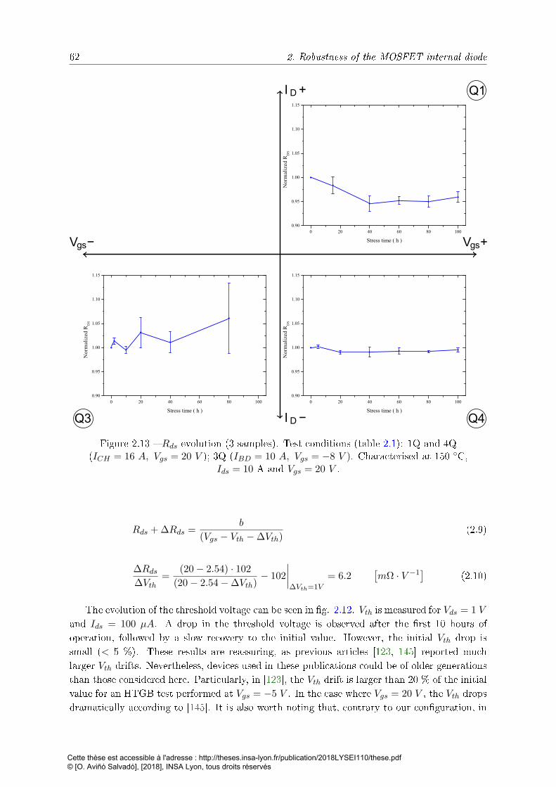
62 2. Robustness of the MOSFET internal diode
Q1
Q3 Q4
Vgs+Vgs−
I D +
I D −
0 20 40 60 80 1000.90
0.95
1.00
1.05
1.10
1.15
Nor
mal
ized
RD
S
Stress time ( h )
0 20 40 60 80 1000.90
0.95
1.00
1.05
1.10
1.15
Nor
mal
ized
RD
S
Stress time ( h )
0 20 40 60 80 1000.90
0.95
1.00
1.05
1.10
1.15
Nor
mal
ized
RD
S
Stress time ( h )
Figure 2.13 Rds evolution (3 samples). Test conditions (table 2.1): 1Q and 4Q(ICH = 16 A, Vgs = 20 V ); 3Q (IBD = 10 A, Vgs = −8 V ). Characterised at 150 C,
Ids = 10 A and Vgs = 20 V .
Rds + ∆Rds =b
(Vgs − Vth −∆Vth)(2.9)
∆Rds∆Vth
=(20− 2.54) · 102
(20− 2.54−∆Vth)− 102
∣∣∣∣∆Vth=1V
= 6.2[mΩ · V −1
](2.10)
The evolution of the threshold voltage can be seen in g. 2.12. Vth is measured for Vds = 1 V
and Ids = 100 µA. A drop in the threshold voltage is observed after the rst 10 hours ofoperation, followed by a slow recovery to the initial value. However, the initial Vth drop issmall (< 5 %). These results are reassuring, as previous articles [123, 145] reported muchlarger Vth drifts. Nevertheless, devices used in these publications could be of older generationsthan those considered here. Particularly, in [123], the Vth drift is larger than 20 % of the initialvalue for an HTGB test performed at Vgs = −5 V . In the case where Vgs = 20 V , the Vth dropsdramatically according to [145]. It is also worth noting that, contrary to our conguration, in
Cette thèse est accessible à l'adresse : http://theses.insa-lyon.fr/publication/2018LYSEI110/these.pdf © [O. Aviñó Salvadó], [2018], INSA Lyon, tous droits réservés
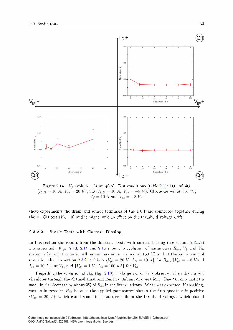
2.3. Static tests 63
Q1
Q3 Q4
Vgs+Vgs−
I D +
I D −
0 20 40 60 80 1000.95
1.00
1.05
1.10
Nor
mal
ized
VF
Stress time ( h )
0 20 40 60 80 1000.95
1.00
1.05
1.10
Nor
mal
ized
VF
Stress time ( h )
0 20 40 60 80 1000.95
1.00
1.05
1.10
Nor
mal
ized
VF
Stress time ( h )
Figure 2.14 Vf evolution (3 samples). Test conditions (table 2.1): 1Q and 4Q(ICH = 16 A, Vgs = 20 V ); 3Q (IBD = 10 A, Vgs = −8 V ). Characterised at 150 C,
If = 10 A and Vgs = −8 V .
these experiments the drain and source terminals of the DUT are connected together duringthe HTGB test (Vds= 0) and it might have an eect on the threshold voltage drift.
2.3.2.2 Static Tests with Current Biasing
In this section the results from the dierent tests with current biasing (see section 2.3.1.3)are presented. Fig. 2.13, 2.14 and 2.15 show the evolution of parameters Rds, Vf and Vthrespectively over the tests. All parameters are measured at 150 C and at the same point ofoperation than in section 2.3.2.1; this is Vgs = 20 V , Ids = 10 A for Rds, Vgs = −8 V andIsd = 10 A for Vf , and Vds = 1 V , Ids = 100 µA for Vth.
Regarding the evolution of Rds (g. 2.13), no large variation is observed when the currentcirculates through the channel (rst and fourth quadrant of operation). One can only notice asmall initial decrease by about 3% of Rds in the rst quadrant. What was expected, if anything,was an increase in Rds because the applied gate-source bias in the rst quadrant is positive(Vgs = 20 V ), which could result in a positive shift in the threshold voltage, which should
Cette thèse est accessible à l'adresse : http://theses.insa-lyon.fr/publication/2018LYSEI110/these.pdf © [O. Aviñó Salvadó], [2018], INSA Lyon, tous droits réservés
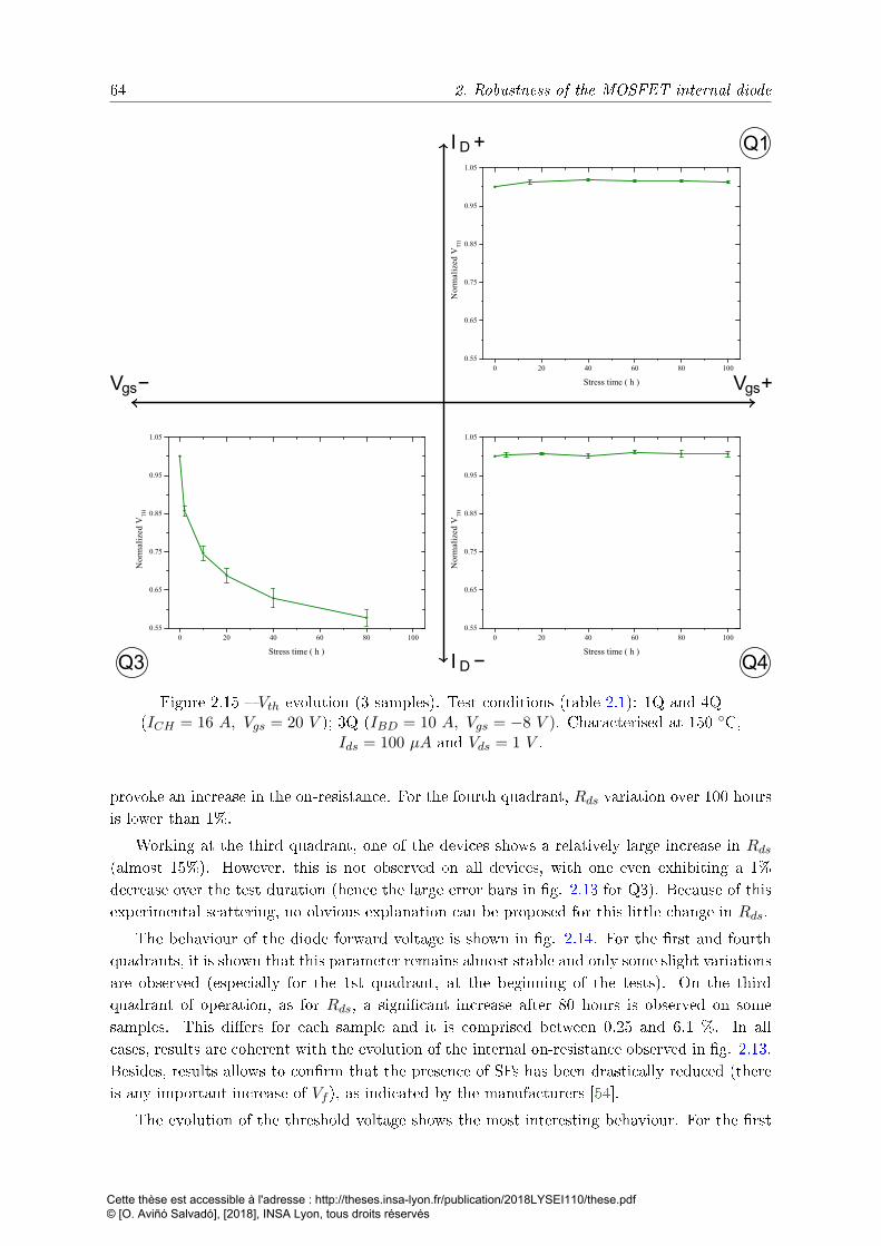
64 2. Robustness of the MOSFET internal diode
Q1
Q3 Q4
Vgs+Vgs−
I D +
I D −
0 20 40 60 80 1000.55
0.65
0.75
0.85
0.95
1.05
Nor
mal
ized
VT
H
Stress time ( h )
0 20 40 60 80 1000.55
0.65
0.75
0.85
0.95
1.05
Nor
mal
ized
VT
H
Stress time ( h )
0 20 40 60 80 1000.55
0.65
0.75
0.85
0.95
1.05
Nor
mal
ized
VT
H
Stress time ( h )
Figure 2.15 Vth evolution (3 samples). Test conditions (table 2.1): 1Q and 4Q(ICH = 16 A, Vgs = 20 V ); 3Q (IBD = 10 A, Vgs = −8 V ). Characterised at 150 C,
Ids = 100 µA and Vds = 1 V .
provoke an increase in the on-resistance. For the fourth quadrant, Rds variation over 100 hoursis lower than 1%.
Working at the third quadrant, one of the devices shows a relatively large increase in Rds(almost 15%). However, this is not observed on all devices, with one even exhibiting a 1%decrease over the test duration (hence the large error bars in g. 2.13 for Q3). Because of thisexperimental scattering, no obvious explanation can be proposed for this little change in Rds.
The behaviour of the diode forward voltage is shown in g. 2.14. For the rst and fourthquadrants, it is shown that this parameter remains almost stable and only some slight variationsare observed (especially for the 1st quadrant, at the beginning of the tests). On the thirdquadrant of operation, as for Rds, a signicant increase after 80 hours is observed on somesamples. This diers for each sample and it is comprised between 0.25 and 6.1 %. In allcases, results are coherent with the evolution of the internal on-resistance observed in g. 2.13.Besides, results allows to conrm that the presence of SFs has been drastically reduced (thereis any important increase of Vf ), as indicated by the manufacturers [54].
The evolution of the threshold voltage shows the most interesting behaviour. For the rst
Cette thèse est accessible à l'adresse : http://theses.insa-lyon.fr/publication/2018LYSEI110/these.pdf © [O. Aviñó Salvadó], [2018], INSA Lyon, tous droits réservés
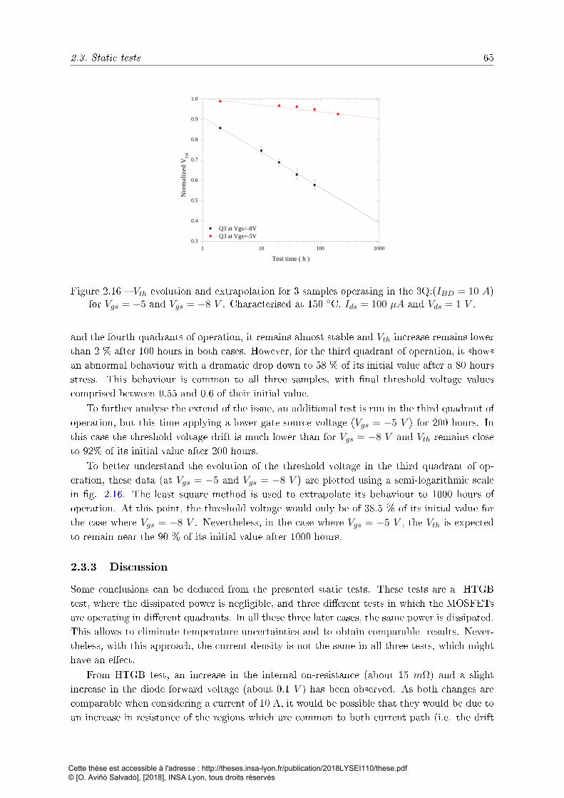
2.3. Static tests 65
1 1 0 1 0 0 1 0 0 00 . 3
0 . 4
0 . 5
0 . 6
0 . 7
0 . 8
0 . 9
1 . 0
Q 3 a t V g s = - 8 V Q 3 a t V g s = - 5 V
Norm
alized
V TH
T e s t t i m e ( h )
Figure 2.16 Vth evolution and extrapolation for 3 samples operating in the 3Q:(IBD = 10 A)for Vgs = −5 and Vgs = −8 V . Characterised at 150 C, Ids = 100 µA and Vds = 1 V .
and the fourth quadrants of operation, it remains almost stable and Vth increase remains lowerthan 2 % after 100 hours in both cases. However, for the third quadrant of operation, it showsan abnormal behaviour with a dramatic drop down to 58 % of its initial value after a 80 hoursstress. This behaviour is common to all three samples, with nal threshold voltage valuescomprised between 0.55 and 0.6 of their initial value.
To further analyse the extend of the issue, an additional test is run in the third quadrant ofoperation, but this time applying a lower gate-source voltage (Vgs = −5 V ) for 200 hours. Inthis case the threshold voltage drift is much lower than for Vgs = −8 V and Vth remains closeto 92% of its initial value after 200 hours.
To better understand the evolution of the threshold voltage in the third quadrant of op-eration, these data (at Vgs = −5 and Vgs = −8 V ) are plotted using a semi-logarithmic scalein g. 2.16. The least square method is used to extrapolate its behaviour to 1000 hours ofoperation. At this point, the threshold voltage would only be of 38.5 % of its initial value forthe case where Vgs = −8 V . Nevertheless, in the case where Vgs = −5 V , the Vth is expectedto remain near the 90 % of its initial value after 1000 hours.
2.3.3 Discussion
Some conclusions can be deduced from the presented static tests. These tests are a HTGBtest, where the dissipated power is negligible, and three dierent tests in which the MOSFETsare operating in dierent quadrants. In all these three later cases, the same power is dissipated.This allows to eliminate temperature uncertainties and to obtain comparable results. Never-theless, with this approach, the current density is not the same in all three tests, which mighthave an eect.
From HTGB test, an increase in the internal on-resistance (about 15 mΩ) and a slightincrease in the diode forward voltage (about 0.1 V ) has been observed. As both changes arecomparable when considering a current of 10 A, it would be possible that they would be due toan increase in resistance of the regions which are common to both current path (i.e. the drift
Cette thèse est accessible à l'adresse : http://theses.insa-lyon.fr/publication/2018LYSEI110/these.pdf © [O. Aviñó Salvadó], [2018], INSA Lyon, tous droits réservés
66 2. Robustness of the MOSFET internal diode
region, the metalization in the packaging). However, these hypotheses have not been conrmedby the other static test (Q1,Q3,Q4). These tests, contrary to HTGB, do not show any consistentinternal on-resistance increase. The most probable reason for this dierent behaviour is thatalthough all devices under test are Wolfspeed SiC MOSFETs C2M008012D [152], they werepurchased separately and those used for the HTGB test [149] are older3. More recently deviceshad probably been improved. We consider that the test realized at the third quadrant ofoperation has to be almost as demanding as the HTGB test, as in both cases Tj = 150 C andVgs = −8 V , but besides it incorporates a current ow which stresses the drift region but notthe channel.
Tests realized in the rst and fourth quadrant of operation do not show any remarkablephenomenon, and in all cases Rds, Vf and Vth remain essentially stable. However, when devicesoperate in the third quadrant, a signicant increase in the internal on-resistance is reported insome cases as well as an important decrease of the Vth.
For one of the samples, the Rds increase reaches close to 14 % of the initial value (about150 mΩ at 150 C for Vgs = 20 V and Ids = 10 A). This increase is comparable with thatreported in the diode forward voltage, which in one sample reaches 6 % (the typical Vf value isabout 3.7 V at 150 C for Vgs = −8 V and Ids = 10 A). A sensibility calculus of ∆Rds(∆Vth)
(see eq. (2.8) to (2.10)) reported that it should be necessary a change of about 1 V in theVth to obtain a variation about 6 mΩ. As obtained results are inconsistent with this orderof magnitude, it is not possible to associate the change in the Rds to that of the Vth, andconsequently to a variation of the channel resistance.
From the Vf and Vth behaviour, two main conclusions can be drawn from the devices testedin the third quadrant of operation:
Stacking Fault (SF) defects have been drastically reduced. As introduced in section 2.2,it has been reported that the use of the internal diode can cause the apparition of basal planedislocation which could result in stacking faults (SF) defects [153, 154]. Thus, as the diodevoltage forward increase after stress is not signicant (<6 %) compared with results reportedon the literature (see g. 2.2 [145]), it can be concluded that crystal quality has been improved,signicantly reducing SF.
An unexpected and dramatic threshold voltage drop occurs. It shows a decreasing ex-ponential behaviour, reaching between 55 and 60 % of the initial value after a stress of 80 hoursin all cases. Extrapolating this behaviour to 1000 hours, it is found that the threshold voltagewould drop to 38.5 % of its initial value, as shown in g. 2.16. This would make the deviceless robust to electromagnetic perturbations. Thus, the probability of a short-circuit event orfailure would increase. Even, in an extreme case, the device could become normally-on.
As shown, to minimize this drop in the threshold voltage, it is possible to apply a dierent Vgs(-5 V instead of -8 V ). Again, this results in lower EMC immunity, requiring a very good setupof the converter to avoid spurious turn-on.
As the threshold voltage has drastically decreased only for the Q3 test, some dierencesbetween the dierent tests must be considered. For Q1 and Q4 test, the device is underconditions of high inversion. In these conditions, with a positive electric eld applied between
3Wolfspeed has been found to modify its devices without reecting the changes in the part reference number,which remained identical.
Cette thèse est accessible à l'adresse : http://theses.insa-lyon.fr/publication/2018LYSEI110/these.pdf © [O. Aviñó Salvadó], [2018], INSA Lyon, tous droits réservés
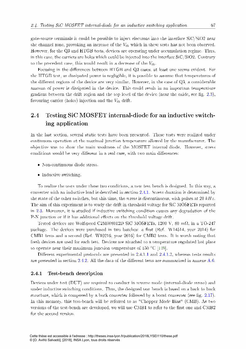
2.4. Testing SiC MOSFET internal-diode for an inductive switching application 67
gate-source terminals it could be possible to inject electrons into the interface SiC/SiO2 nearthe channel zone, provoking an increase of the Vth which in these tests has not been observed.However, for the Q3 and HTGB tests, devices are operating under accumulation regime. Thus,in this case, the carriers are holes which could be injected into the interface SiC/SiO2. Contraryto the precedent case, this would result in a decrease of the Vth.
Focusing in the dierences between HTGB and Q3 cases, at least one seems evident. Forthe HTGB test, as dissipated power is negligible, it is possible to assume that temperatures ofthe dierent regions of the device are very similar. However, in the case of Q3, a considerableamount of power is dissipated in the device. This could result in an important temperaturegradient between the drift region and the top level of the device (near the oxide, see g. 2.3),favouring carrier (holes) injection and the Vth drift.
2.4 Testing SiC MOSFET internal-diode for an inductive switch-
ing application
In the last section, several static tests have been presented. These tests were realized undercontinuous operation at the maximal junction temperature allowed by the manufacturer. Theobjective was to show the main weakness of the MOSFET internal-diode. However, stressconditions would be very dierent in a real case, with two main dierences:
Non-continuous diode stress.
Inductive switching.
To realize the tests under these two conditions, a new test-bench is designed. In this way, aconverter with an inductive load is described in section 2.4.1. Stress duration is determined bythe state of the other switches, but this time, the stress is discontinuous, with pulses at 20 kHz.The aim of this experiment is to study the drift in threshold voltage for SiC MOSFETs reportedin 2.3. Moreover, it is studied if inductive switching condition causes any degradation of theP-N junction or if it has additional eects on the threshold voltage drift.
Tested devices are Wolfspeed C2M008012D SiC MOSFETs, 1200 V, 80 mΩ, in a TO-247package. The devices were purchased in two batches: a rst (Ref. W14514, year 2014) forCMB1 tests and a second (Ref. W10216, year 2016) for CMB2 tests. It is worth noting thatfresh devices are used for each test. Devices are attached to a temperature-regulated hot plateto operate near their maximum junction temperature of 150 C [149].
Dierent experimental protocols are presented in 2.4.1.1 and 2.4.1.2, whereas tests resultsare presented in section 2.4.2. All the data of the dierent tests are summarized in annexe A.6.
2.4.1 Test-bench description
Devices under test (DUT) are required to conduct in reverse mode (internal-diode stress) andunder inductive switching conditions. Thus, the designed test-bench is based on a back-to-backstructure, which is composed by a buck converter followed by a boost converter (see g. 2.17).In this memory, this test-bench will be referred to as "Chopper Mode Bias" (CMB). As twoversions of the test-bench are developed, we will use CMB1 to refer to the rst one and CMB2for the second version.
Cette thèse est accessible à l'adresse : http://theses.insa-lyon.fr/publication/2018LYSEI110/these.pdf © [O. Aviñó Salvadó], [2018], INSA Lyon, tous droits réservés

68 2. Robustness of the MOSFET internal diode
−+
540 V
Vdd
M1
DUT
D1
M2
L1
C
L2
−+-8 V
Vgs
R
Vp1
R
Vp2
R
Figure 2.17 Schematic of the back to back test-bench (CMB).
The current in the boost converter inductor (L2) is regulated to 10 A by the duty cycle ofM2. This imposes the same current to the buck inductor (L1), and therefore to the DUT whenit is involved. Both inductors L1 and L2 have a value of 80 mH. This high inductance valuewill assure a low current ripple for the chosen frequency (f=20 kHz), but also guarantees highlyinductive commutations. Moreover, a capacitor of 27 µF is placed between these two inductorsto minimize perturbations and to simplify the control of the system.
To illustrate the amplitude of the current ripple, we can consider a duty cycle (D) of M1.During the time when this switch is conducting (50% of the period), the inductor currentincreases. Considering that capacitance voltage (Vc) is stable at 50% of the input voltage(540 V ), current will increase by 0.084 A in agreement with (2.11). When the state of theswitches changes, the current decreases by the same value. Thus, the current ripple is smallenough to be neglected.
∆Ipp 'Vdd − Vc
L· Df
=540− 270
80 · 10−3· 0.5
20 · 103= 0.084 A (2.11)
Fig. 2.18 shows a simplied circuit diagram of the CMB test-bench, where the boostconverter is modelled as a 10 A continuous current source (Isw). The chosen input voltage isVdd = 540 V because this is the voltage chosen for the more electric aircraft high voltage DCbus (HVDC) [17, 18]. Thus, it allows to test the device in the same conditions of operation asin a real avionic application.
Using the same test-bench, two dierent tests are realized. These are presented in sections2.4.1.1 and 2.4.1.2. For the rst one, the channel of the DUT remains always blocked and thecurrent only ows through the internal diode. For the second test, the DUT is periodicallyturned-on and the current also ows through the channel, depending of the applied duty cycle.The objective is to determine if the duty cycle has any impact on the threshold voltage drift.
2.4.1.1 CMB Test -Channel always blocked-
The aim of this test is to assess an eventual degradation of the P-N junction, as well as athreshold voltage drift. The gate voltage is xed at a constant negative voltage, forcing theMOSFET in the o-state and the current to ow through the intrinsic diode. As the converter
Cette thèse est accessible à l'adresse : http://theses.insa-lyon.fr/publication/2018LYSEI110/these.pdf © [O. Aviñó Salvadó], [2018], INSA Lyon, tous droits réservés
2.4. Testing SiC MOSFET internal-diode for an inductive switching application 69
−+540 V
Vdd
M1
DUTIsw
10 A−+-8 V
Vgs
R
Vp1
R
Figure 2.18 Simplied CMB schematic, modelling the boost converter as a continuouscurrent source.
is working in continuous conduction mode, there are dierent circuit congurations dependingon the state of switches (M1 and DUT). These are detailed below together with the junctiontemperature estimation.
Some rst measurements are performed at Vgs = −5 V and show important perturbationson the gate-source voltage. Thus, gate-source DUT voltage is xed to Vgs = −8 V to ensurethat EMC perturbations are not capable to cause a short-circuit event. It is worth notingthat the datasheets [149, 152] mention an absolute minimal Vgs = −10 V . However, the latestdatasheet version [152] recommends a Vgs = −5 V for applications involving the internal diode.Nevertheless, this is not mandatory and the absolute minimal Vgs level remains -10 V.
A complete characterization of the devices under test at room temperature is realized every20 hours after a cooling-down time of 1 hour. Devices are also characterized after the rst 10hours. Total test duration is 100 hours. As a threshold voltage drift is observed, the test hasbeen prolonged up to 400 hours for four components.
Moreover, to study deeply this drift of the threshold voltage, the test is run on SiC MOS-FETs from two additional manufacturers, with the same voltage and similar current range.Chosen devices are SCT2080KE from ROHM4 [155] and SCT30N120 from ST5 [156]. In bothcases, the test is run on three samples. It is noticeable that ROHM MOSFET is blocked atVgs = −5 V , as its datasheet limits the minimal Vgs to -6 V [155]. For the ST MOSFET, testis run at Vgs = −8 V , as for the Wolfspeed devices (it is limited at -10 V [156]).
Finally, a second test-bench (CMB2) has been developed to minimize gate-source voltageperturbations. It is based on the same circuit structure, but parasitic inductances and capaci-tances on the power and driver PCBs have been minimized. This better EMC design, allowedto reduce signicantly the perturbations, especially on the gate-source voltage. Using this test-bench, two additional test runs are performed. The rst one at Vgs = −8 V and the secondone at Vgs = −5 V . In both cases, the test are run on three samples. Unfortunately, in spiteof the perturbation reduction, in the case where Vgs = −5 V , two samples have fail during thetest. Anyway these rst characterization points indicate a trend. All details about both CMBtest-benches are presented in annexe A.5.
4ROHM refers to ROHM Semiconductor5ST refers to STMicroelectronics
Cette thèse est accessible à l'adresse : http://theses.insa-lyon.fr/publication/2018LYSEI110/these.pdf © [O. Aviñó Salvadó], [2018], INSA Lyon, tous droits réservés
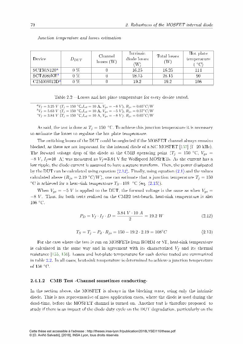
70 2. Robustness of the MOSFET internal diode
Junction temperature and losses estimation
Device DDUTChannellosses (W)
Intrinsicdiode losses
(W)
Total losses(W)
Hot platetemperature
( C)SCT30N120a 0 % 0 16.25 16.25 114SCT2080KEb 0 % 0 28.15 28.15 90C2M008012Dc 0 % 0 19.2 19.2 108
Table 2.2 Losses and hot plate temperature for every device tested.
aVf = 3.25 V (Tj = 150 C,Isd = 10 A, Vgs = −8 V ), Rjc = 0.65C/WbVf = 5.63 V (Tj = 150 C,Isd = 10 A, Vgs = −5 V ), Rjc = 0.57C/WcVf = 3.84 V (Tj = 150 C,Isd = 10 A, Vgs = −8 V ), Rjc = 0.65C/W
As said, the test is done at Tj = 150 C. To achieve this junction temperature it is necessaryto estimate the losses to regulate the hot plate temperature.
The switching losses of the DUT could be neglected if the MOSFET channel always remainsblocked, as these are not important for the internal diode of a SiC MOSFET [157] (f=20 kHz).The forward voltage drop of the diode at the CMB operating point (Tj = 150 C, Vgs =
−8 V , If=10 A) was measured as Vf=3.84 V for Wolfspeed MOSFETs. As the current has alow ripple, the diode current is assumed to have a square waveform. Then, the power dissipatedby the DUT can be calculated using equation (2.12). Finally, using equation (2.1) and the valuescalculated above (Rjs = 2.19 C/W ), one can estimate that a junction temperature Tj = 150C is achieved for a heat-sink temperature TS=108 C (eq. (2.13)).
When Vgs = −5 V is applied to the DUT, the forward voltage is the same as when Vgs =
−8 V . Thus, for both tests realized on the CMB2 test-bench, heat-sink temperature is also108 C.
PD = Vf · If ·D =3.84 V · 10 A
2= 19.2 W (2.12)
TS = Tj − Pd ·Rjs = 150− 19.2 · 2.19 = 108C (2.13)
For the case where the test is run on MOSFETs from ROHM or ST, heat-sink temperatureis calculated in the same way and in agreement with its characterized Vf and its thermalresistance [155, 156]. Losses and hot-plate temperature for each device tested are summarizedin table 2.2. In all cases, heat-sink temperature is determined to achieve a junction temperatureof 150 C.
2.4.1.2 CMB Test -Channel sometimes conducting-
In the section above, the MOSFET is always in the blocking state, using only the intrinsicdiode. This is not representative of most application cases, where the diode is used during thedead-time, before the MOSFET channel is turned on. Another test is therefore proposed tostudy if there is an impact of the diode duty cycle on the DUT degradation, particularly on the
Cette thèse est accessible à l'adresse : http://theses.insa-lyon.fr/publication/2018LYSEI110/these.pdf © [O. Aviñó Salvadó], [2018], INSA Lyon, tous droits réservés
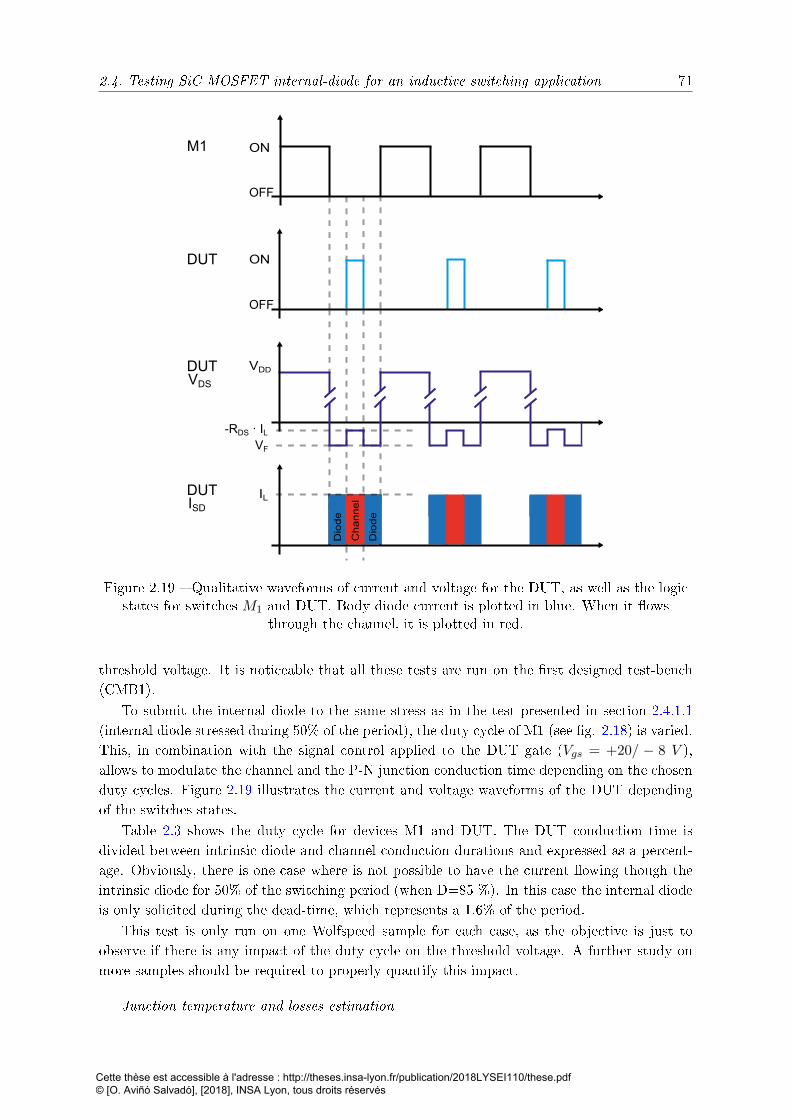
2.4. Testing SiC MOSFET internal-diode for an inductive switching application 71
M1
DUT
VDS
ON
OFF
ON
OFF
VDD
-RDS · ILVF
IL
DUT
ISD
DUT
Ch
an
ne
l
Dio
de
Dio
de
Figure 2.19 Qualitative waveforms of current and voltage for the DUT, as well as the logicstates for switches M1 and DUT. Body diode current is plotted in blue. When it ows
through the channel, it is plotted in red.
threshold voltage. It is noticeable that all these tests are run on the rst designed test-bench(CMB1).
To submit the internal diode to the same stress as in the test presented in section 2.4.1.1(internal diode stressed during 50% of the period), the duty cycle of M1 (see g. 2.18) is varied.This, in combination with the signal control applied to the DUT gate (Vgs = +20/ − 8 V ),allows to modulate the channel and the P-N junction conduction time depending on the chosenduty cycles. Figure 2.19 illustrates the current and voltage waveforms of the DUT dependingof the switches states.
Table 2.3 shows the duty cycle for devices M1 and DUT. The DUT conduction time isdivided between intrinsic diode and channel conduction durations and expressed as a percent-age. Obviously, there is one case where is not possible to have the current owing though theintrinsic diode for 50% of the switching period (when D=85 %). In this case the internal diodeis only solicited during the dead-time, which represents a 1.6% of the period.
This test is only run on one Wolfspeed sample for each case, as the objective is just toobserve if there is any impact of the duty cycle on the threshold voltage. A further study onmore samples should be required to properly quantify this impact.
Junction temperature and losses estimation
Cette thèse est accessible à l'adresse : http://theses.insa-lyon.fr/publication/2018LYSEI110/these.pdf © [O. Aviñó Salvadó], [2018], INSA Lyon, tous droits réservés
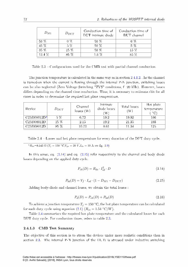
72 2. Robustness of the MOSFET internal diode
DM1 DDUTConduction time ofDUT intrinsic diode
Conduction time ofDUT channel
50 % 0 % 50 % 0 %45 % 5 % 50 % 5 %35 % 15 % 50 % 15 %13.4 % 85 % 1.6 % 85 %
Table 2.3 Congurations used for the CMB test with partial channel conduction.
The junction temperature is calculated in the same way as in section 2.4.1.2. As the channelis turned-on when the current is owing through the internal P-N junction, switching lossescan be also neglected (Zero Voltage Switching "ZVS" conditions, f=20 kHz). However, lossesdiers depending on the channel time conduction. Thus, it is necessary to estimate this for allcases in order to determine the required hot plate temperature.
Device DDUTChannellosses (W)
Intrinsicdiode losses
(W)
Total losses(W)
Hot platetemperature
( C)C2M008012Da 5 % 0.72 19.2 19.92 106C2M008012D 15 % 2.15 19.2 21.35 103C2M008012D 85 % 10.73 0.61 11.34 125
Table 2.4 Losses and hot plate temperature for every duration of the DUT duty cycle.
aRds=0.143 Ω (Tj = 150 C,Vgs = 20 V ,Ids = 10 A see g. 2.9)
In this sense, eq. (2.14) and eq. (2.15) refer respectively to the channel and body diodelosses depending on the applied duty cycle.
Pch(D) = Rds · I2sd ·D (2.14)
Pbd(D) = Vf · Isd · (1−DM1 −DDUT ) (2.15)
Adding body-diode and channel losses, we obtain the total losses :
Pd(D) = Pch(D) + Pbd(D) (2.16)
To achieve a junction temperature Tj = 150 C, the hot plate temperature can be calculatedfor each duty cycle using equation (2.1) (Rcs = 1.54 C/W ).
Table 2.4 summarizes the required hot plate temperature and the calculated losses for eachDUT duty cycle. For conduction times, refers to table 2.3.
2.4.1.3 CMB Test Summary
The objective of this section is to stress the devices under more realistic conditions than insection 2.3. The internal P-N junction of the DUTs is stressed under inductive switching
Cette thèse est accessible à l'adresse : http://theses.insa-lyon.fr/publication/2018LYSEI110/these.pdf © [O. Aviñó Salvadó], [2018], INSA Lyon, tous droits réservés
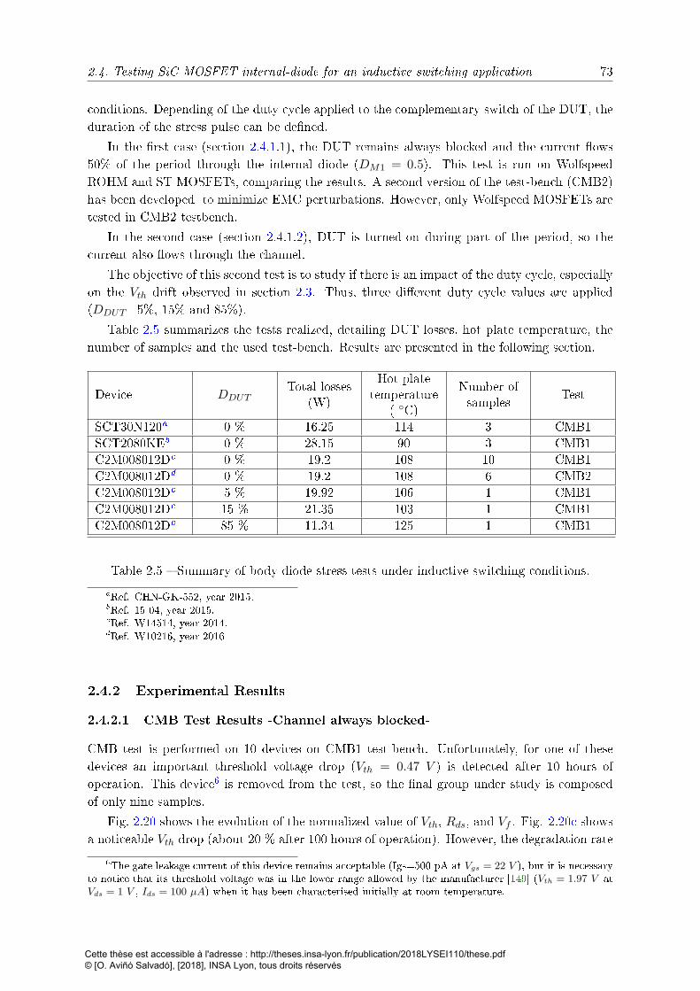
2.4. Testing SiC MOSFET internal-diode for an inductive switching application 73
conditions. Depending of the duty cycle applied to the complementary switch of the DUT, theduration of the stress pulse can be dened.
In the rst case (section 2.4.1.1), the DUT remains always blocked and the current ows50% of the period through the internal diode (DM1 = 0.5). This test is run on WolfspeedROHM and ST MOSFETs, comparing the results. A second version of the test-bench (CMB2)has been developed to minimize EMC perturbations. However, only Wolfspeed MOSFETs aretested in CMB2 testbench.
In the second case (section 2.4.1.2), DUT is turned-on during part of the period, so thecurrent also ows through the channel.
The objective of this second test is to study if there is an impact of the duty cycle, especiallyon the Vth drift observed in section 2.3. Thus, three dierent duty cycle values are applied(DDUT=5%, 15% and 85%).
Table 2.5 summarizes the tests realized, detailing DUT losses, hot plate temperature, thenumber of samples and the used test-bench. Results are presented in the following section.
Device DDUTTotal losses
(W)
Hot platetemperature
( C)
Number ofsamples
Test
SCT30N120a 0 % 16.25 114 3 CMB1SCT2080KEb 0 % 28.15 90 3 CMB1C2M008012Dc 0 % 19.2 108 10 CMB1C2M008012Dd 0 % 19.2 108 6 CMB2C2M008012Dc 5 % 19.92 106 1 CMB1C2M008012Dc 15 % 21.35 103 1 CMB1C2M008012Dc 85 % 11.34 125 1 CMB1
Table 2.5 Summary of body diode stress tests under inductive switching conditions.
aRef. CHN-GK-552, year 2015.bRef. 15-04, year 2015.cRef. W14514, year 2014.dRef. W10216, year 2016
2.4.2 Experimental Results
2.4.2.1 CMB Test Results -Channel always blocked-
CMB test is performed on 10 devices on CMB1 test-bench. Unfortunately, for one of thesedevices an important threshold voltage drop (Vth = 0.47 V ) is detected after 10 hours ofoperation. This device6 is removed from the test, so the nal group under study is composedof only nine samples.
Fig. 2.20 shows the evolution of the normalized value of Vth, Rds, and Vf . Fig. 2.20c showsa noticeable Vth drop (about 20 % after 100 hours of operation). However, the degradation rate
6The gate leakage current of this device remains acceptable (Igs=500 pA at Vgs = 22 V ), but it is necessaryto notice that its threshold voltage was in the lower range allowed by the manufacturer [149] (Vth = 1.97 V atVds = 1 V , Ids = 100 µA) when it has been characterised initially at room temperature.
Cette thèse est accessible à l'adresse : http://theses.insa-lyon.fr/publication/2018LYSEI110/these.pdf © [O. Aviñó Salvadó], [2018], INSA Lyon, tous droits réservés
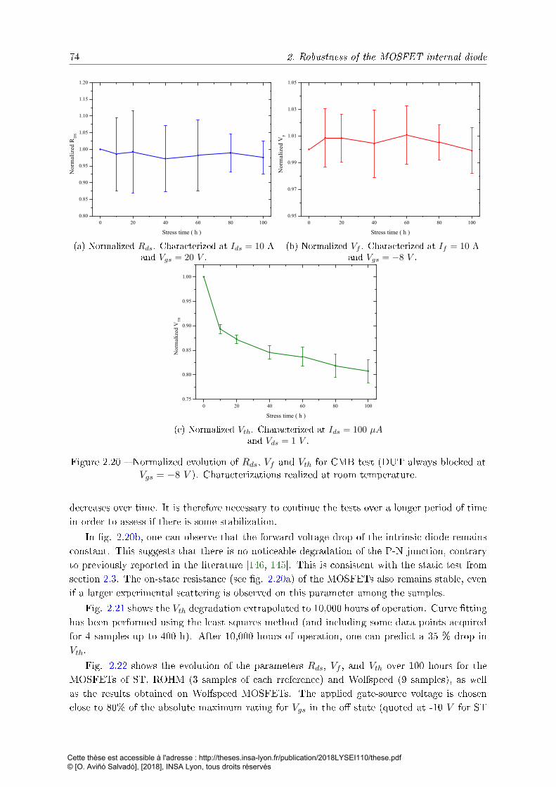
74 2. Robustness of the MOSFET internal diode
0 20 40 60 80 1000.80
0.85
0.90
0.95
1.00
1.05
1.10
1.15
1.20
Nor
mal
ized
RD
S
Stress time ( h )
(a) Normalized Rds. Characterized at Ids = 10 Aand Vgs = 20 V .
0 20 40 60 80 1000.95
0.97
0.99
1.01
1.03
1.05
Nor
mal
ized
VF
Stress time ( h )
(b) Normalized Vf . Characterized at If = 10 Aand Vgs = −8 V .
0 20 40 60 80 1000.75
0.80
0.85
0.90
0.95
1.00
Nor
mal
ized
VT
H
Stress time ( h )
(c) Normalized Vth. Characterized at Ids = 100 µAand Vds = 1 V .
Figure 2.20 Normalized evolution of Rds, Vf and Vth for CMB test (DUT always blocked atVgs = −8 V ). Characterizations realized at room temperature.
decreases over time. It is therefore necessary to continue the tests over a longer period of timein order to assess if there is some stabilization.
In g. 2.20b, one can observe that the forward voltage drop of the intrinsic diode remainsconstant. This suggests that there is no noticeable degradation of the P-N junction, contraryto previously reported in the literature [146, 145]. This is consistent with the static test fromsection 2.3. The on-state resistance (see g. 2.20a) of the MOSFETs also remains stable, evenif a larger experimental scattering is observed on this parameter among the samples.
Fig. 2.21 shows the Vth degradation extrapolated to 10,000 hours of operation. Curve ttinghas been performed using the least squares method (and including some data points acquiredfor 4 samples up to 400 h). After 10,000 hours of operation, one can predict a 35 % drop inVth.
Fig. 2.22 shows the evolution of the parameters Rds, Vf , and Vth over 100 hours for theMOSFETs of ST, ROHM (3 samples of each rreference) and Wolfspeed (9 samples), as wellas the results obtained on Wolfspeed MOSFETs. The applied gate-source voltage is chosenclose to 80% of the absolute maximum rating for Vgs in the o state (quoted at -10 V for ST
Cette thèse est accessible à l'adresse : http://theses.insa-lyon.fr/publication/2018LYSEI110/these.pdf © [O. Aviñó Salvadó], [2018], INSA Lyon, tous droits réservés
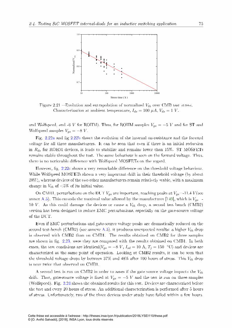
2.4. Testing SiC MOSFET internal-diode for an inductive switching application 75
10 100 1000 10000
0.7
0.8
0.9
1.0
Nor
mal
ized
VT
H
Stress time ( h )
Figure 2.21 Evolution and extrapolation of normalized Vth over CMB test stress.Characterization at ambient temperature, Ids = 100 µA, Vds = 1 V .
and Wolfspeed, and -6 V for ROHM). Thus, for ROHM samples Vgs = −5 V and for ST andWolfspeed samples Vgs = −8 V .
Fig. 2.22a and g 2.22b shows the evolution of the internal on-resistance and the forwardvoltage for all three manufacturers. It can be seen that even if there is an initial reductionin Rds for ROHM devices, it leads to stabilize and remains lower than 15%. ST MOSFETsremains stable throughout the test. The same behaviour is seen on the forward voltage. Thus,there is no noticeable dierence with Wolfspeed MOSFETs on the regard.
However, g. 2.22c shows a very remarkable dierence on the threshold voltage behaviour.While Wolfspeed MOSFETs shown a very important drift in their threshold voltage (by about20%), whereas devices of the two other manufacturers remain relatively stable, with a maximumchange in Vth of <5% of its initial value.
On CMB1, perturbations on the DUT Vgs are important, reaching peaks at Vgs=-11.4 V (seeannex A.5). This exceeds the maximal value allowed by the manufacturer [149], which is Vgs=-10 V . As this could damage the devices or cause a Vth drop, a second test-bench (CMB2)version has been designed to reduce EMC perturbations, especially on the gate-source voltageof the DUT.
Even if EMC perturbations and gate-source voltage peaks are dramatically reduced on thesecond test-bench (CMB2) (see annexe A.5), it produces unexpected results: a higher Vth dropis observed with CMB2 than on CMB1. The results obtained on CMB2 for three samplesare shown in g. 2.23, were they are compared with the results obtained on CMB1. In bothcases, the test conditions are identical(Vgs = −8 V , Isd = 10 A, Tj = 150 C) and devices arecharacterized at the same point of operation. Looking at CMB2 results, it can be seen thatthe threshold voltage drops by between 37% and 48% after 100 hours of stress. This Vth dropis near twice that observed on CMB1.
A second test is run on CMB2 in order to asses if the gate-source voltage impacts the Vthdrift. Thus, gate-source voltage is xed at Vgs = −5 V and the test is run on three samples(Wolfspeed). Fig. 2.24 shows the obtained results for this test. Devices are characterized beforethe test and every 20 hours of stress. An additional characterization is performed after 5 hoursof stress. Unfortunately, two of the three devices under study have failed within a few hours.
Cette thèse est accessible à l'adresse : http://theses.insa-lyon.fr/publication/2018LYSEI110/these.pdf © [O. Aviñó Salvadó], [2018], INSA Lyon, tous droits réservés
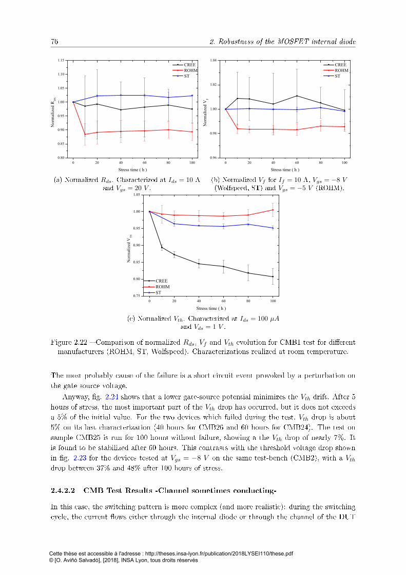
76 2. Robustness of the MOSFET internal diode
0 20 40 60 80 1000.80
0.85
0.90
0.95
1.00
1.05
1.10
1.15
Nor
mal
ized
HRD
S
StressHtimeH(HhH)
CREEROHMST
(a) Normalized Rds. Characterized at Ids = 10 Aand Vgs = 20 V .
0 20 40 60 80 1000.96
0.98
1.00
1.02
1.04
Nor
mal
ized
HVF
StressHtimeH(HhH)
CREEROHMST
(b) Normalized Vf for If = 10 A, Vgs = −8 V(Wolfspeed, ST) and Vgs = −5 V (ROHM).
0 20 40 60 80 1000.75
0.80
0.85
0.90
0.95
1.00
1.05
Nor
mal
ized
RVT
H
StressRtimeR(RhR)
CREEROHMST
(c) Normalized Vth. Characterized at Ids = 100 µAand Vds = 1 V .
Figure 2.22 Comparison of normalized Rds, Vf and Vth evolution for CMB1 test for dierentmanufacturers (ROHM, ST, Wolfspeed). Characterizations realized at room temperature.
The most probably cause of the failure is a short-circuit event provoked by a perturbation onthe gate-source voltage.
Anyway, g. 2.24 shows that a lower gate-source potential minimizes the Vth drift. After 5hours of stress, the most important part of the Vth drop has occurred, but it does not exceedsa 5% of the initial value. For the two devices which failed during the test, Vth drop is about5% on its last characterization (40 hours for CMB26 and 60 hours for CMB24). The test onsample CMB25 is run for 100 hours without failure, showing a the Vth drop of nearly 7%. Itis found to be stabilized after 60 hours. This contrasts with the threshold voltage drop shownin g. 2.23 for the devices tested at Vgs = −8 V on the same test-bench (CMB2), with a Vthdrop between 37% and 48% after 100 hours of stress.
2.4.2.2 CMB Test Results -Channel sometimes conducting-
In this case, the switching pattern is more complex (and more realistic): during the switchingcycle, the current ows either through the internal diode or through the channel of the DUT
Cette thèse est accessible à l'adresse : http://theses.insa-lyon.fr/publication/2018LYSEI110/these.pdf © [O. Aviñó Salvadó], [2018], INSA Lyon, tous droits réservés

2.4. Testing SiC MOSFET internal-diode for an inductive switching application 77
0 20 40 60 80 1000.5
0.6
0.7
0.8
0.9
1.0CMB2CMB1
Nor
mal
ized
hVT
H
Stresshtimeh(hhh)
Figure 2.23 Evolution of normalized Vth over CMB test stress for CMB1 and CMB2test-bench (Vgs = −8 V ). Characterization at ambient temperature, Ids = 100 µA, Vds = 1 V .
0 10 20 30 40 50 60 70 80 90 1000.92
0.93
0.94
0.95
0.96
0.97
0.98
0.99
1.00
1.01
Nor
mal
ized
DVT
H
StressDtimeD(DhD)
DUTDCMB24DUTDCMB25DUTDCMB26
Figure 2.24 Evolution of normalized Vth over CMB test stress (test-bench CMB2,Vgs = −5 V ) for three samples. Characterization at ambient temperature, Ids = 100 µA,
Vds = 1 V .
(see table 2.3 and g. 2.19). The test is run on only one sample for each test condition (D=0.05,D=0.15 and D=0.85), but it clearly shows a dierent Vth drift for the dierent duty cycles.Further studies may be realised for more accurate results. The test is performed using the rstversion of the test-bench, not on the improved one (see annexe A.5) and at Vgs = +20/− 8 V .
Fig. 2.25 shows the evolution of Rds, Vf and Vth for dierent duty cycles (D). Internalon-resistance (g. 2.25a) and forward voltage (g. 2.25b) remain almost stable with changes ofless than 3% and 1% respectively after 100 hours of stress. Measurement points after 20 hoursfor D=0.15 and after 40 hours for D=0.05 presents aberrant errors.
The most remarkable is the inuence of the duty cycle (D) on the threshold voltage degra-dation, which is shown in g. 2.25c. The cases where D=0 (which corresponds to the testspresented in the previous section), D=0.05 and D=0.15 are fully comparable with each other, asthe conduction time through the intrinsic diode remains at 50% of the switching cycle (20 kHz).It is observed that for a low duty cycle (5 or 15 %), the threshold voltage shows a weak negativedrift and seems to stabilize rapidly.
Cette thèse est accessible à l'adresse : http://theses.insa-lyon.fr/publication/2018LYSEI110/these.pdf © [O. Aviñó Salvadó], [2018], INSA Lyon, tous droits réservés
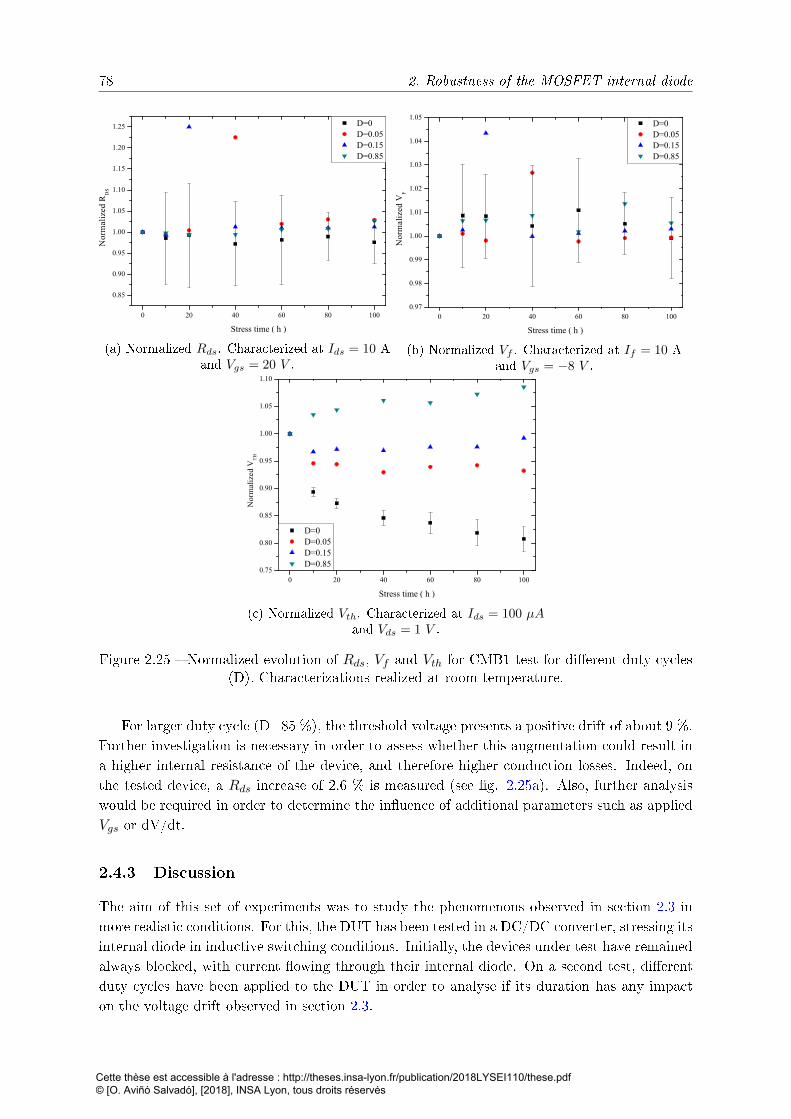
78 2. Robustness of the MOSFET internal diode
0 20 40 60 80 100
0.85
0.90
0.95
1.00
1.05
1.10
1.15
1.20
1.25 D=0D=0.05D=0.15D=0.85
Nor
mal
ized
RD
S
Stress time ( h )
(a) Normalized Rds. Characterized at Ids = 10 Aand Vgs = 20 V .
0 20 40 60 80 1000.97
0.98
0.99
1.00
1.01
1.02
1.03
1.04
1.05D=0D=0.05D=0.15D=0.85
Nor
mal
ized
)VF
Stress)time)()h))
(b) Normalized Vf . Characterized at If = 10 Aand Vgs = −8 V .
0 20 40 60 80 1000.75
0.80
0.85
0.90
0.95
1.00
1.05
1.10
D=0D=0.05D=0.15D=0.85
Nor
mal
ized
)VT
H
Stress)time)()h))
(c) Normalized Vth. Characterized at Ids = 100 µAand Vds = 1 V .
Figure 2.25 Normalized evolution of Rds, Vf and Vth for CMB1 test for dierent duty cycles(D). Characterizations realized at room temperature.
For larger duty cycle (D=85 %), the threshold voltage presents a positive drift of about 9 %.Further investigation is necessary in order to assess whether this augmentation could result ina higher internal resistance of the device, and therefore higher conduction losses. Indeed, onthe tested device, a Rds increase of 2.6 % is measured (see g. 2.25a). Also, further analysiswould be required in order to determine the inuence of additional parameters such as appliedVgs or dV/dt.
2.4.3 Discussion
The aim of this set of experiments was to study the phenomenons observed in section 2.3 inmore realistic conditions. For this, the DUT has been tested in a DC/DC converter, stressing itsinternal diode in inductive switching conditions. Initially, the devices under test have remainedalways blocked, with current owing through their internal diode. On a second test, dierentduty cycles have been applied to the DUT in order to analyse if its duration has any impacton the voltage drift observed in section 2.3.
Cette thèse est accessible à l'adresse : http://theses.insa-lyon.fr/publication/2018LYSEI110/these.pdf © [O. Aviñó Salvadó], [2018], INSA Lyon, tous droits réservés
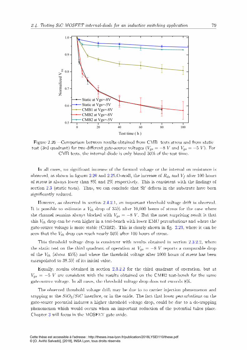
2.4. Testing SiC MOSFET internal-diode for an inductive switching application 79
0 20 40 60 80 1000.5
0.6
0.7
0.8
0.9
1.0
Nor
mal
ized
gVT
H
Testgtimeg(ghg)
StaticgatgVgs=-8VStaticgatgVgs=-5VCMB1gatgVgs=-8VCMB2gatgVgs=-8VCMB2gatgVgs=-5V
Figure 2.26 Comparison between results obtained from CMB tests stress and from statictest (3rd quadrant) for two dierent gate-source voltages (Vgs = −8 V and Vgs = −5 V ). For
CMB tests, the internal diode is only biased 50% of the test time.
In all cases, no signicant increase of the forward voltage or the internal on-resistance isobserved, as shown in gures 2.20 and 2.25.Overall, the increase of Rds and Vf after 100 hoursof stress is always lower than 8% and 2% respectively. This is consistent with the ndings ofsection 2.3 (static tests). Thus, we can conclude that SF defects in the substrate have beensignicantly reduced.
However, as observed in section 2.4.2.1, an important threshold voltage drift is observed.It is possible to estimate a Vth drop of 35% after 10,000 hours of stress for the case wherethe channel remains always blocked with Vgs = −8 V . But the most surprising result is thatthis Vth drop can be even higher in a test-bench with lower EMC perturbations and where thegate-source voltage is more stable (CMB2). This is clearly shown in g. 2.23, where it can beseen that the Vth drop can reach nearly 50% after 100 hours of stress.
This threshold voltage drop is consistent with results obtained in section 2.3.2.2, wherethe static test on the third quadrant of operation at Vgs = −8 V reports a comparable dropof the Vth (about 45%) and where the threshold voltage after 1000 hours of stress has beenextrapolated to 38.5% of its initial value.
Equally, results obtained in section 2.3.2.2 for the third quadrant of operation, but atVgs = −5 V are consistent with the results obtained on the CMB2 test-bench for the samegate-source voltage. In all cases, the threshold voltage drop does not exceeds 8%.
The observed threshold voltage drift may be due to to carrier injection phenomenon andtrapping at the SiO2/SiC interface, or in the oxide. The fact that lower perturbations on thegate-source potential induces a higher threshold voltage drop, could be due to a de-trappingphenomenon which would occurs when an important reduction of the potential takes place.Chapter 3 will focus in the MOSFET gate oxide.
Cette thèse est accessible à l'adresse : http://theses.insa-lyon.fr/publication/2018LYSEI110/these.pdf © [O. Aviñó Salvadó], [2018], INSA Lyon, tous droits réservés
80 2. Robustness of the MOSFET internal diode
Further analysis, applying dierent duty cycles to the DUT, are realized. It shows that theduty cycle has an important impact on the threshold voltage stability.
On the one side, for a small duty cycle (5 or 15%), threshold voltage decreases weakly duringthe rst hours of stress and then remains stable. The maximum Vth drop is 8% after 100 hoursfor the case where D=0.05. On the other side, for a relatively high duty cycle (D=0.85), Vthshows a increase of about 9% after 100 hours of stress. It is noticeable that according to table2.3, in this last case the internal P-N junction is stressed for a very short time.
The weak threshold voltage drop in the cases where a the duty cycle is no longer 0, but itremains small (5 or 15%), could be explained by the same de-trapping phenomenon as in thecase where important perturbations appears on the gate-source voltage (reducing the appliedgate-source potential).
Further studies should investigate the case where a large duty cycle is applied, as for thecase where D=0.85, which reports an increase of about 9% on the threshold voltage. It couldbe thought that this is due to a trapping phenomenon when a high electric eld is applied for along time, but this has not been observed with the static tests (1st and 4th quadrant) presentedin section 2.3.2.2.
2.5 Conclusions
The main objective of this chapter was to study the robustness of the internal P-N junctionof SiC MOSFETs, for their posible utilisation in diode-less applications. Obtained resultshighlighs that the intrinsic diode does not show any a signicant degradation when it is used.This diers from previous reports in the literature, and may indicate an improvement in theSiC substrate quality, with a reduction of its defect density as reported in recent years [158,159]. Among these defects there are the basal plane dislocations or stacking faults, which wouldcause degradation of the P-N junction.
However, an unexpected drift of the threshold voltage has been observed. Presumably, it isdue to carrier injection and trapping at the SiO2/SiC interface, or in the oxide. This injectiondepends on the polarity of the voltage applied at the gate, as well as on the application time(i.e. the duty cycle).
Carrier injection phenomenon are related to the electric eld as well as to the barrier height.We nd that when the device is blocked at Vgs = −5 V the Vth drift is much lower than whenit is blocked at Vgs = −8 V . Thus, a threshold factor appears. In g. 2.26 it can be seen thatthere is no signicant dierence between the Vth drift observed on the CMB2 test stress andon the static tests (3rd quadrant of operation). Thus, repetitive inductive switching does notcause a noticeable degradation.
However, this degradation of the threshold voltage has not been observed during the statictests where the internal diode is not solicited (1st and 4th quadrant of operation), nor during thestandard HTGB test. Thus, further study is required about this, especially taking in accountthat a positive Vth drift has been observed in CMB test stress in the case when a high dutycycle is applied (D=0.85).
Another remarkable issue is that perturbations on the gate-source voltage may induce ade-trapping phenomenon, due to a temporary lower potential applied between the gate-sourceterminals. This minimizes the observed Vth drift, as it has been shown in g. 2.23. In the same
Cette thèse est accessible à l'adresse : http://theses.insa-lyon.fr/publication/2018LYSEI110/these.pdf © [O. Aviñó Salvadó], [2018], INSA Lyon, tous droits réservés
2.5. Conclusions 81
way, as soon as the duty cycle is not zero, there is a gate-source polarity inversion which willtrigger this de-trapping phenomenon. Thus, also in this case Vth drift is minimized.
In a real application case, the diode is only used during a small fraction of the overallswitching cycle (during dead-times). Therefore, and taking in account that gate-source polaritywill not be always negative, we can conclude that it is possible to use the internal diodeinstead of adding an external diode (diode-less applications). Anyway, Wolfspeed MOSFETsC2M0080120D seem to be more sensitive to this phenomenon that their competitors and requirefurther tests, especially at extremes duty cycle.
The experiments presented here show that the standard JEDEC tests used on silicon IGBTand MOSFETs are not fully suited to SiC devices. The degradation observed of the gate oxide,both on static and CMB tests is indeed not revealed by standard HTGB tests. Thus, standardtests must be revised or new tests must be added to the qualify procedures.
Regarding the driving circuit, and to prevent short-circuit problems which may arise from areduction in threshold voltage, the use of a negative voltage to block the device is recommended.However, care must be given in the choice of the negative Vgs level, as a larger value, althoughit would give a better EMI immunity, may cause Vth to drift faster. In the case of WolfspeedMOSFETs, it was found that Vgs = −5 V is more suitable than Vgs = −8 V . This nding isconrmed by the most recent datasheet from Wolfspeed, where a Vgs = −5 V is recommendedfor applications where the body diode is used.
Future work should include a larger number of samples to obtain more reliable results,based on samples from several manufacturers as well as on the newest generations of devices,as they tend to improve rapidly. Furthmore, as shown by the dierent results acquired fromboth versions of the CMB setup, Vgs itself is not the only parameter which has an inuenceon the Vth drift. ∆Vgs/∆t or EMI transient also may have an eect which must be assessed infuture studies.
Cette thèse est accessible à l'adresse : http://theses.insa-lyon.fr/publication/2018LYSEI110/these.pdf © [O. Aviñó Salvadó], [2018], INSA Lyon, tous droits réservés

Cette thèse est accessible à l'adresse : http://theses.insa-lyon.fr/publication/2018LYSEI110/these.pdf © [O. Aviñó Salvadó], [2018], INSA Lyon, tous droits réservés
Chapter 3
Robustness of the MOSFET gate oxide
Contents
3.1 Introduction . . . . . . . . . . . . . . . . . . . . . . . . . . . . . . . . 83
3.2 Degradation of the Gate Oxide . . . . . . . . . . . . . . . . . . 84
3.2.1 Bias Temperature Instability - BTI - . . . . . . . . . . . . . . . . . . 84
3.2.2 Time Dependent Dielectric Breakdown - TDDB - . . . . . . . . . . . 85
3.3 Study of the bias temperature instability -BTI- . . . . 87
3.3.1 Experimental Methodology . . . . . . . . . . . . . . . . . . . . . . . 87
3.3.2 Experimental Results . . . . . . . . . . . . . . . . . . . . . . . . . . . 91
3.3.3 Discussion . . . . . . . . . . . . . . . . . . . . . . . . . . . . . . . . . 92
3.4 Estimation of gate oxide breakdown time -TDDB- . . . 93
3.4.1 Experimental Methodology . . . . . . . . . . . . . . . . . . . . . . . 94
3.4.2 Experimental Results . . . . . . . . . . . . . . . . . . . . . . . . . . . 98
3.4.3 Discussion . . . . . . . . . . . . . . . . . . . . . . . . . . . . . . . . . 104
3.5 Conclusions . . . . . . . . . . . . . . . . . . . . . . . . . . . . . . . . . 106
3.1 Introduction
In spite of the better properties of SiC versus Si, which were shown in chapter 1, SiC powerMOSFETs are just penetrating into industrial applications. This is due to their lack of maturityand some reliability issues which were also introduced in that same chapter. One of theseissues is related to the oxide layer and more particularly to the SiC/SiO2 interface, as it washighlighted in chapter 2. This chapter focuses on the behaviour of this oxide layer, which evenif it is identical in chemical composition as the oxide used in Si MOSFETs (SiO2), is weakerdue to its smaller thickness (thus, supporting a higher electric eld) and lower energy banddierence with SiC.
As it was presented in chap. 1, gate robustness is related to the SiO2 insulator layerlocated between the gate terminal and the drift region. In this chapter, we focus on the twomain measurements used to asses the degradation of the gate oxide:
Bias Temperature Instability - BTI
Time Dependent Dielectric Breakdown - TDDB
In a rst time, we study bias temperature instabilities on commercial SiC MOSFETs.The objective of this study is to asses if the Vth drift observed in some cases in chapter 2, isreproduced here. Moreover, the gate leakage current is measured in order to evaluate if thisparameter can be used to assess the gate oxide degradation.
Cette thèse est accessible à l'adresse : http://theses.insa-lyon.fr/publication/2018LYSEI110/these.pdf © [O. Aviñó Salvadó], [2018], INSA Lyon, tous droits réservés
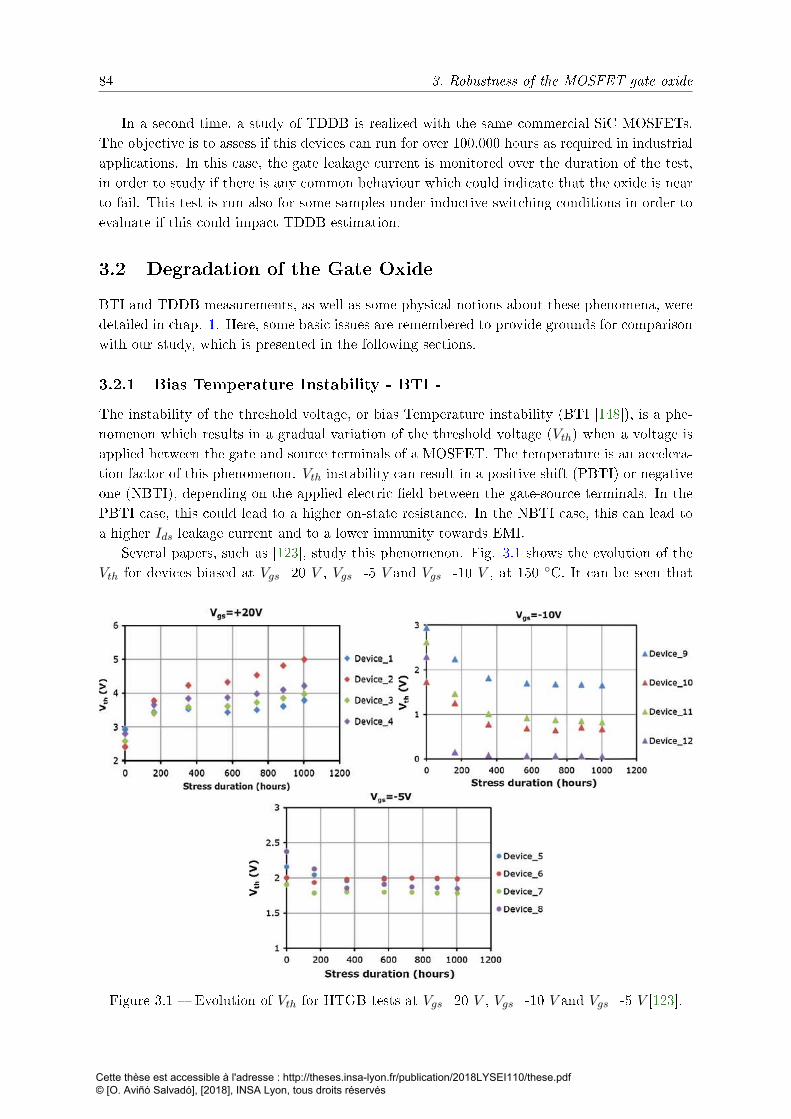
84 3. Robustness of the MOSFET gate oxide
In a second time, a study of TDDB is realized with the same commercial SiC MOSFETs.The objective is to assess if this devices can run for over 100.000 hours as required in industrialapplications. In this case, the gate leakage current is monitored over the duration of the test,in order to study if there is any common behaviour which could indicate that the oxide is nearto fail. This test is run also for some samples under inductive switching conditions in order toevaluate if this could impact TDDB estimation.
3.2 Degradation of the Gate Oxide
BTI and TDDB measurements, as well as some physical notions about these phenomena, weredetailed in chap. 1. Here, some basic issues are remembered to provide grounds for comparisonwith our study, which is presented in the following sections.
3.2.1 Bias Temperature Instability - BTI -
The instability of the threshold voltage, or bias Temperature instability (BTI [148]), is a phe-nomenon which results in a gradual variation of the threshold voltage (Vth) when a voltage isapplied between the gate and source terminals of a MOSFET. The temperature is an accelera-tion factor of this phenomenon. Vth instability can result in a positive shift (PBTI) or negativeone (NBTI), depending on the applied electric eld between the gate-source terminals. In thePBTI case, this could lead to a higher on-state resistance. In the NBTI case, this can lead toa higher Ids leakage current and to a lower immunity towards EMI.
Several papers, such as [123], study this phenomenon. Fig. 3.1 shows the evolution of theVth for devices biased at Vgs=20 V , Vgs=-5 V and Vgs=-10 V , at 150 C. It can be seen that
Figure 3.1 Evolution of Vth for HTGB tests at Vgs=20 V , Vgs=-10 V and Vgs=-5 V [123].
Cette thèse est accessible à l'adresse : http://theses.insa-lyon.fr/publication/2018LYSEI110/these.pdf © [O. Aviñó Salvadó], [2018], INSA Lyon, tous droits réservés
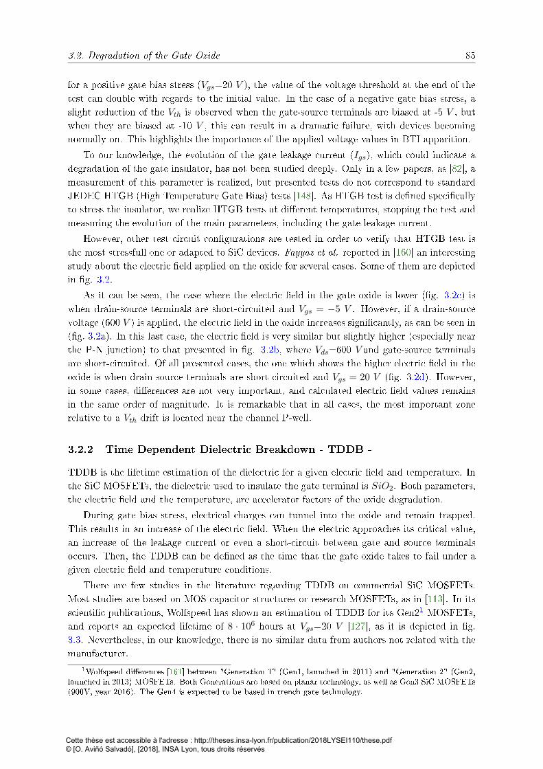
3.2. Degradation of the Gate Oxide 85
for a positive gate bias stress (Vgs=20 V ), the value of the voltage threshold at the end of thetest can double with regards to the initial value. In the case of a negative gate bias stress, aslight reduction of the Vth is observed when the gate-source terminals are biased at -5 V , butwhen they are biased at -10 V , this can result in a dramatic failure, with devices becomingnormally-on. This highlights the importance of the applied voltage values in BTI apparition.
To our knowledge, the evolution of the gate leakage current (Igs), which could indicate adegradation of the gate insulator, has not been studied deeply. Only in a few papers, as [82], ameasurement of this parameter is realized, but presented tests do not correspond to standardJEDEC HTGB (High Temperature Gate Bias) tests [148]. As HTGB test is dened specicallyto stress the insulator, we realize HTGB tests at dierent temperatures, stopping the test andmeasuring the evolution of the main parameters, including the gate leakage current.
However, other test circuit congurations are tested in order to verify that HTGB test isthe most stressfull one or adapted to SiC devices. Fayyaz et al. reported in [160] an interestingstudy about the electric eld applied on the oxide for several cases. Some of them are depictedin g. 3.2.
As it can be seen, the case where the electric eld in the gate oxide is lower (g. 3.2c) iswhen drain-source terminals are short-circuited and Vgs = −5 V . However, if a drain-sourcevoltage (600 V ) is applied, the electric eld in the oxide increases signicantly, as can be seen in(g. 3.2a). In this last case, the electric eld is very similar but slightly higher (especially nearthe P-N junction) to that presented in g. 3.2b, where Vds=600 V and gate-source terminalsare short-circuited. Of all presented cases, the one which shows the higher electric eld in theoxide is when drain-source terminals are short-circuited and Vgs = 20 V (g. 3.2d). However,in some cases, dierences are not very important, and calculated electric eld values remainsin the same order of magnitude. It is remarkable that in all cases, the most important zonerelative to a Vth drift is located near the channel P-well.
3.2.2 Time Dependent Dielectric Breakdown - TDDB -
TDDB is the lifetime estimation of the dielectric for a given electric eld and temperature. Inthe SiC MOSFETs, the dielectric used to insulate the gate terminal is SiO2. Both parameters,the electric eld and the temperature, are accelerator factors of the oxide degradation.
During gate bias stress, electrical charges can tunnel into the oxide and remain trapped.This results in an increase of the electric eld. When the electric approaches its critical value,an increase of the leakage current or even a short-circuit between gate and source terminalsoccurs. Then, the TDDB can be dened as the time that the gate oxide takes to fail under agiven electric eld and temperature conditions.
There are few studies in the literature regarding TDDB on commercial SiC MOSFETs.Most studies are based on MOS capacitor structures or research MOSFETs, as in [113]. In itsscientic publications, Wolfspeed has shown an estimation of TDDB for its Gen21 MOSFETs,and reports an expected lifetime of 8 · 106 hours at Vgs=20 V [127], as it is depicted in g.3.3. Nevertheless, in our knowledge, there is no similar data from authors not related with themanufacturer.
1Wolfspeed dierences [161] between "Generation 1" (Gen1, launched in 2011) and "Generation 2" (Gen2,launched in 2013) MOSFETs. Both Generations are based on planar technology, as well as Gen3 SiC MOSFETs(900V, year 2016). The Gen4 is expected to be based in trench gate technology.
Cette thèse est accessible à l'adresse : http://theses.insa-lyon.fr/publication/2018LYSEI110/these.pdf © [O. Aviñó Salvadó], [2018], INSA Lyon, tous droits réservés
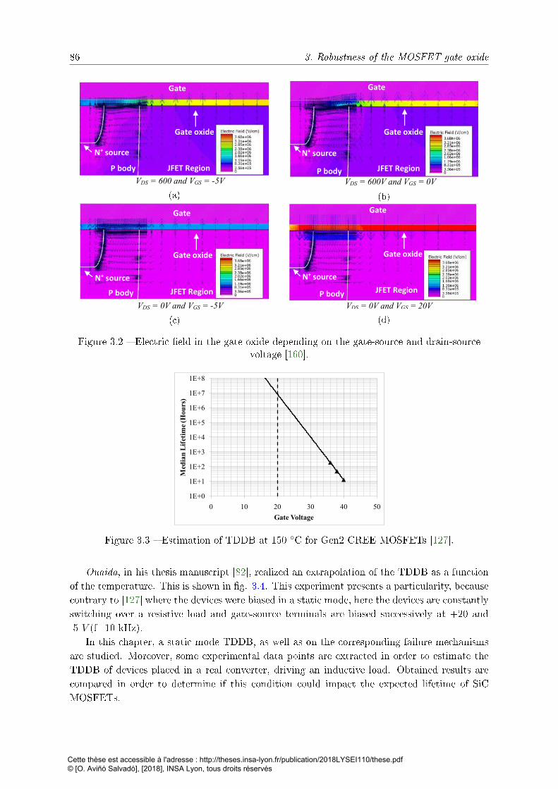
86 3. Robustness of the MOSFET gate oxide
(a) (b)
(c) (d)
Figure 3.2 Electric eld in the gate oxide depending on the gate-source and drain-sourcevoltage [160].
1E+0
1E+1
1E+2
1E+3
1E+4
1E+5
1E+6
1E+7
1E+8
0 10 20 30 40 50
Med
ian
Lif
etim
e (H
ours
)
Gate Voltage
Figure 3.3 Estimation of TDDB at 150 C for Gen2 CREE MOSFETs [127].
Ouaida, in his thesis manuscript [82], realized an extrapolation of the TDDB as a functionof the temperature. This is shown in g. 3.4. This experiment presents a particularity, becausecontrary to [127] where the devices were biased in a static mode, here the devices are constantlyswitching over a resistive load and gate-source terminals are biased successively at +20 and-5 V (f=10 kHz).
In this chapter, a static mode TDDB, as well as on the corresponding failure mechanismsare studied. Moreover, some experimental data points are extracted in order to estimate theTDDB of devices placed in a real converter, driving an inductive load. Obtained results arecompared in order to determine if this condition could impact the expected lifetime of SiCMOSFETs.
Cette thèse est accessible à l'adresse : http://theses.insa-lyon.fr/publication/2018LYSEI110/these.pdf © [O. Aviñó Salvadó], [2018], INSA Lyon, tous droits réservés
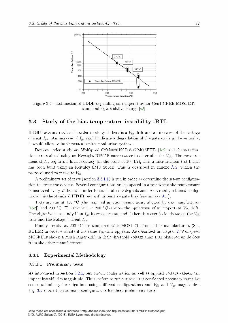
3.3. Study of the bias temperature instability -BTI- 87
Figure 3.4 Estimation of TDDB depending on temperature for Gen1 CREE MOSFETscommanding a resistive charge [82].
3.3 Study of the bias temperature instability -BTI-
HTGB tests are realized in order to study if there is a Vth drift and an increase of the leakagecurrent Igs. An increase of Igs could indicate a degradation of the gate oxide and eventually,it would allow to implement a health monitoring system.
Devices under study are Wolfspeed C2M0080120D SiC MOSFETs [152] and characteriza-tions are realized using an Keysight B1505B curve tracer to determine the Vth. The measure-ment of Igs requires a high accuracy (in the order of 100 fA), thus a measurement test-benchhas been built using an Keithley SMU 2636B. This is described in annexe A.2, within theprotocol used to measure Vth.
A preliminary set of tests (section 3.3.1.1) is run in order to determine the set-up congura-tion to stress the devices. Several congurations are compared in a test where the temperatureis increased every 24 hours in order to accelerate the degradation. As a result, retained cong-uration is the standard HTGB test with a positive gate bias (see annexe A.1).
Tests are run at 150 C (the maximal junction temperature allowed by the manufacturer[152]) and 200 C. The test run at 200 C ensures the apparition of an important Vth drift.The objective is to study if an Igs increase occurs, and if there is a correlation between the Vthdrift and the leakage current Igs.
Finally, results at 200 C are compared with MOSFETs from other manufacturers (ST,ROHM) in order evaluate if the same Vth drift appears. As described in chapter 2, WolfspeedMOSFETs shown a much larger drift in their threshold voltage than that observed on devicesfrom the other manufacturers.
3.3.1 Experimental Methodology
3.3.1.1 Preliminary tests
As introduced in section 3.2.1, test circuit conguration as well as applied voltage values, canimpact instabilities magnitude. Thus, before to run our test, it is considered necessary to realizesome preliminary investigations using dierent congurations and Vds and Vgs magnitudes.Fig. 3.5 shows the two main congurations for these preliminary tests.
Cette thèse est accessible à l'adresse : http://theses.insa-lyon.fr/publication/2018LYSEI110/these.pdf © [O. Aviñó Salvadó], [2018], INSA Lyon, tous droits réservés
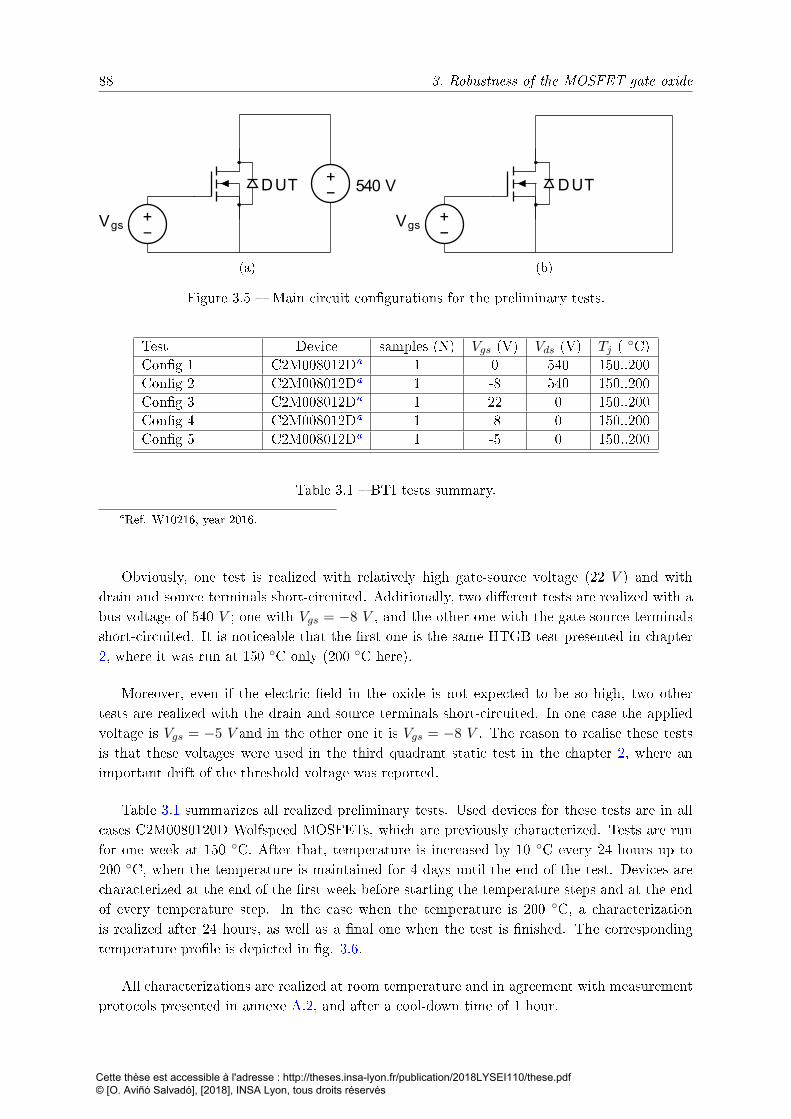
88 3. Robustness of the MOSFET gate oxide
DUT
−+Vgs
−+ 540 V
(a)
DUT
−+Vgs
(b)
Figure 3.5 Main circuit congurations for the preliminary tests.
Test Device samples (N) Vgs (V) Vds (V) Tj ( C)Cong 1 C2M008012Da 1 0 540 150..200Cong 2 C2M008012Da 1 -8 540 150..200Cong 3 C2M008012Da 1 22 0 150..200Cong 4 C2M008012Da 1 -8 0 150..200Cong 5 C2M008012Da 1 -5 0 150..200
Table 3.1 BTI tests summary.
aRef. W10216, year 2016.
Obviously, one test is realized with relatively high gate-source voltage (22 V ) and withdrain and source terminals short-circuited. Additionally, two dierent tests are realized with abus voltage of 540 V ; one with Vgs = −8 V , and the other one with the gate-source terminalsshort-circuited. It is noticeable that the rst one is the same HTGB test presented in chapter2, where it was run at 150 C only (200 C here).
Moreover, even if the electric eld in the oxide is not expected to be so high, two othertests are realized with the drain and source terminals short-circuited. In one case the appliedvoltage is Vgs = −5 V and in the other one it is Vgs = −8 V . The reason to realise these testsis that these voltages were used in the third quadrant static test in the chapter 2, where animportant drift of the threshold voltage was reported.
Table 3.1 summarizes all realized preliminary tests. Used devices for these tests are in allcases C2M0080120D Wolfspeed MOSFETs, which are previously characterized. Tests are runfor one week at 150 C. After that, temperature is increased by 10 C every 24 hours up to200 C, when the temperature is maintained for 4 days until the end of the test. Devices arecharacterized at the end of the rst week before starting the temperature steps and at the endof every temperature step. In the case when the temperature is 200 C, a characterizationis realized after 24 hours, as well as a nal one when the test is nished. The correspondingtemperature prole is depicted in g. 3.6.
All characterizations are realized at room temperature and in agreement with measurementprotocols presented in annexe A.2, and after a cool-down time of 1 hour.
Cette thèse est accessible à l'adresse : http://theses.insa-lyon.fr/publication/2018LYSEI110/these.pdf © [O. Aviñó Salvadó], [2018], INSA Lyon, tous droits réservés
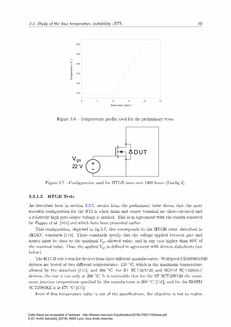
3.3. Study of the bias temperature instability -BTI- 89
0 3 6 9 1 2 1 5
1 5 0
1 6 0
1 7 0
1 8 0
1 9 0
2 0 0
S t r e s s t i m e ( d a y s )
Figure 3.6 Temperature prole used for the preliminary tests.
DUT
−+22 V
Vgs
Figure 3.7 Conguration used for HTGB tests over 1000 hours (Cong 3).
3.3.1.2 HTGB Tests
As described later in section 3.3.2, results from the preliminary tests shown that the moststressful conguration for the BTI is when drain and source terminal are short-circuited anda relatively high gate-source voltage is applied. This is in agreement with the results reportedby Fayyaz et al. [160] and which have been presented earlier.
This conguration, depicted in g.3.7, also corresponds to the HTGB tests, described inJEDEC standards [148]. These standards specify that the voltage applied between gate andsource must be close to the maximal Vgs allowed value, and in any case higher than 80% ofthe maximal value. Thus, the applied Vgs is dened in agreement with devices datasheets (seebelow).
The HTGB test is run for devices from three dierent manufacturers. Wolfspeed C2M0080120Ddevices are tested at two dierent temperatures: 150 C, which is the maximum temperatureallowed by the datasheet [152], and 200 C. For ST SCT30N120 and ROHM SCT2080KEdevices, the test is run only at 200 C. It is noticeable that for the ST SCT30N120 the maxi-mum junction temperature specied by the manufacturer is 200 C [156], and for the ROHMSCT2080KE it is 175 C [155].
Even if this temperature value is out of the specications, the objective is not to realize
Cette thèse est accessible à l'adresse : http://theses.insa-lyon.fr/publication/2018LYSEI110/these.pdf © [O. Aviñó Salvadó], [2018], INSA Lyon, tous droits réservés
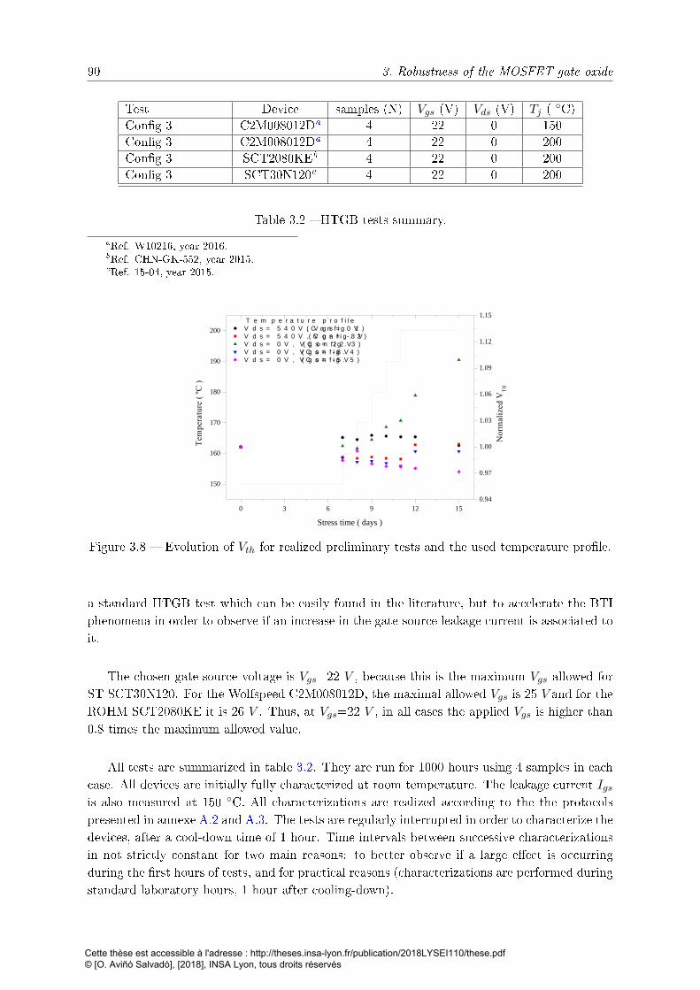
90 3. Robustness of the MOSFET gate oxide
Test Device samples (N) Vgs (V) Vds (V) Tj ( C)Cong 3 C2M008012Da 4 22 0 150Cong 3 C2M008012Da 4 22 0 200Cong 3 SCT2080KEb 4 22 0 200Cong 3 SCT30N120c 4 22 0 200
Table 3.2 HTGB tests summary.
aRef. W10216, year 2016.bRef. CHN-GK-552, year 2015.cRef. 15-04, year 2015.
0 3 6 9 1 2 1 5
1 5 0
1 6 0
1 7 0
1 8 0
1 9 0
2 0 0 T e m p e r a t u r e p r o f i l e V d s = 5 4 0 V , V g s = 0 V ( C o n f i g . 1 ) V d s = 5 4 0 V , V g s = - 8 V ( C o n f i g . 2 ) V d s = 0 V , V g s = 2 2 V ( C o n f i g . 3 ) V d s = 0 V , V g s = - 8 V ( C o n f i g . 4 ) V d s = 0 V , V g s = - 5 V ( C o n f i g . 5 )
S t r e s s t i m e ( d a y s )
0 . 9 4
0 . 9 7
1 . 0 0
1 . 0 3
1 . 0 6
1 . 0 9
1 . 1 2
1 . 1 5
Figure 3.8 Evolution of Vth for realized preliminary tests and the used temperature prole.
a standard HTGB test which can be easily found in the literature, but to accelerate the BTIphenomena in order to observe if an increase in the gate-source leakage current is associated toit.
The chosen gate-source voltage is Vgs=22 V , because this is the maximum Vgs allowed forST SCT30N120. For the Wolfspeed C2M008012D, the maximal allowed Vgs is 25 V and for theROHM SCT2080KE it is 26 V . Thus, at Vgs=22 V , in all cases the applied Vgs is higher than0.8 times the maximum allowed value.
All tests are summarized in table 3.2. They are run for 1000 hours using 4 samples in eachcase. All devices are initially fully characterized at room temperature. The leakage current Igsis also measured at 150 C. All characterizations are realized according to the the protocolspresented in annexe A.2 and A.3. The tests are regularly interrupted in order to characterize thedevices, after a cool-down time of 1 hour. Time intervals between successive characterizationsin not strictly constant for two main reasons: to better observe if a large eect is occurringduring the rst hours of tests, and for practical reasons (characterizations are performed duringstandard laboratory hours, 1 hour after cooling-down).
Cette thèse est accessible à l'adresse : http://theses.insa-lyon.fr/publication/2018LYSEI110/these.pdf © [O. Aviñó Salvadó], [2018], INSA Lyon, tous droits réservés
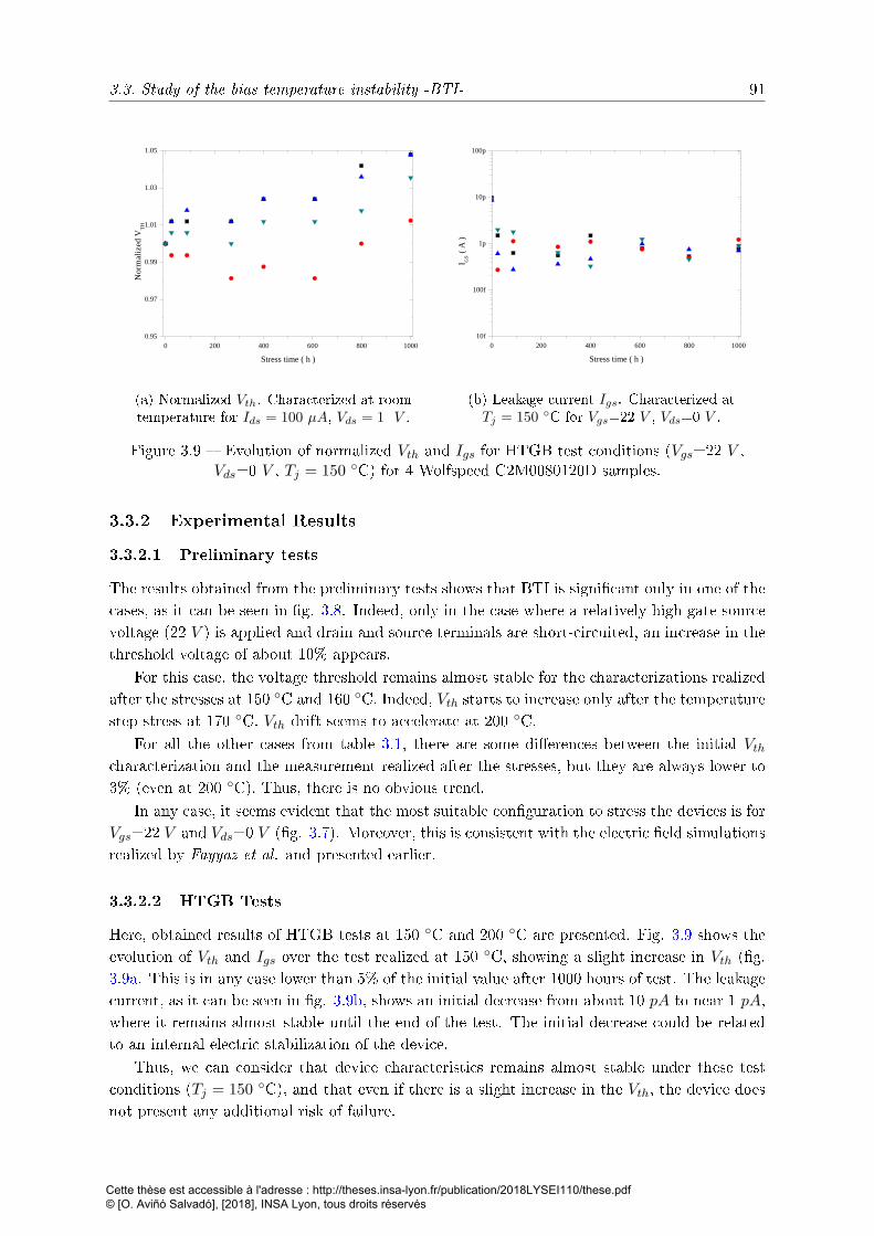
3.3. Study of the bias temperature instability -BTI- 91
0 2 0 0 4 0 0 6 0 0 8 0 0 1 0 0 00 . 9 5
0 . 9 7
0 . 9 9
1 . 0 1
1 . 0 3
1 . 0 5
Norm
alized
V TH
S t r e s s t i m e ( h )
(a) Normalized Vth. Characterized at roomtemperature for Ids = 100 µA, Vds = 1 V .
0 2 0 0 4 0 0 6 0 0 8 0 0 1 0 0 01 0 f
1 0 0 f
1 p
1 0 p
1 0 0 p
I GS ( A
)
S t r e s s t i m e ( h )
(b) Leakage current Igs. Characterized atTj = 150 C for Vgs=22 V , Vds=0 V .
Figure 3.9 Evolution of normalized Vth and Igs for HTGB test conditions (Vgs=22 V ,Vds=0 V , Tj = 150 C) for 4 Wolfspeed C2M0080120D samples.
3.3.2 Experimental Results
3.3.2.1 Preliminary tests
The results obtained from the preliminary tests shows that BTI is signicant only in one of thecases, as it can be seen in g. 3.8. Indeed, only in the case where a relatively high gate-sourcevoltage (22 V ) is applied and drain and source terminals are short-circuited, an increase in thethreshold voltage of about 10% appears.
For this case, the voltage threshold remains almost stable for the characterizations realizedafter the stresses at 150 C and 160 C. Indeed, Vth starts to increase only after the temperaturestep stress at 170 C. Vth drift seems to accelerate at 200 C.
For all the other cases from table 3.1, there are some dierences between the initial Vthcharacterization and the measurement realized after the stresses, but they are always lower to3% (even at 200 C). Thus, there is no obvious trend.
In any case, it seems evident that the most suitable conguration to stress the devices is forVgs=22 V and Vds=0 V (g. 3.7). Moreover, this is consistent with the electric eld simulationsrealized by Fayyaz et al. and presented earlier.
3.3.2.2 HTGB Tests
Here, obtained results of HTGB tests at 150 C and 200 C are presented. Fig. 3.9 shows theevolution of Vth and Igs over the test realized at 150 C, showing a slight increase in Vth (g.3.9a. This is in any case lower than 5% of the initial value after 1000 hours of test. The leakagecurrent, as it can be seen in g. 3.9b, shows an initial decrease from about 10 pA to near 1 pA,where it remains almost stable until the end of the test. The initial decrease could be relatedto an internal electric stabilization of the device.
Thus, we can consider that device characteristics remains almost stable under these testconditions (Tj = 150 C), and that even if there is a slight increase in the Vth, the device doesnot present any additional risk of failure.
Cette thèse est accessible à l'adresse : http://theses.insa-lyon.fr/publication/2018LYSEI110/these.pdf © [O. Aviñó Salvadó], [2018], INSA Lyon, tous droits réservés
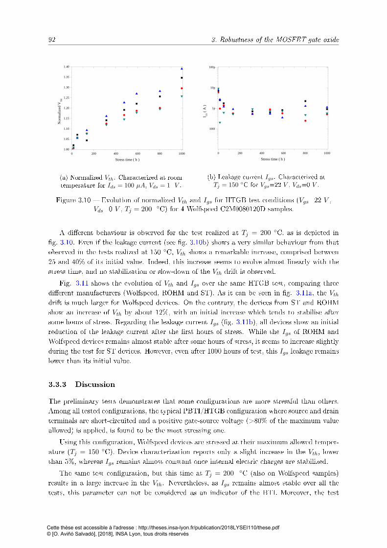
92 3. Robustness of the MOSFET gate oxide
0 2 0 0 4 0 0 6 0 0 8 0 0 1 0 0 01 . 0 0
1 . 0 5
1 . 1 0
1 . 1 5
1 . 2 0
1 . 2 5
1 . 3 0
1 . 3 5
1 . 4 0
Norm
alized
V TH
S t r e s s t i m e ( h )
(a) Normalized Vth. Characterized at roomtemperature for Ids = 100 µA, Vds = 1 V .
0 2 0 0 4 0 0 6 0 0 8 0 0 1 0 0 0
1 0 0 f
1 p
1 0 p
1 0 0 p
I GS ( A
)
S t r e s s t i m e ( h )
(b) Leakage current Igs. Characterized atTj = 150 C for Vgs=22 V , Vds=0 V .
Figure 3.10 Evolution of normalized Vth and Igs for HTGB test conditions (Vgs=22 V ,Vds=0 V , Tj = 200 C) for 4 Wolfspeed C2M0080120D samples.
A dierent behaviour is observed for the test realized at Tj = 200 C, as is depicted ing. 3.10. Even if the leakage current (see g. 3.10b) shows a very similar behaviour from thatobserved in the tests realized at 150 C, Vth shows a remarkable increase, comprised between25 and 40% of its initial value. Indeed, this increase seems to evolve almost linearly with thestress time, and no stabilization or slow-down of the Vth drift is observed.
Fig. 3.11 shows the evolution of Vth and Igs over the same HTGB test, comparing threedierent manufacturers (Wolfspeed, ROHM and ST). As it can be seen in g. 3.11a, the Vthdrift is much larger for Wolfspeed devices. On the contrary, the devices from ST and ROHMshow an increase of Vth by about 12%, with an initial increase which tends to stabilise aftersome hours of stress. Regarding the leakage current Igs (g. 3.11b), all devices show an initialreduction of the leakage current after the rst hours of stress. While the Igs of ROHM andWolfspeed devices remains almost stable after some hours of stress, it seems to increase slightlyduring the test for ST devices. However, even after 1000 hours of test, this Igs leakage remainslower than its initial value.
3.3.3 Discussion
The preliminary tests demonstrates that some congurations are more stressful than others.Among all tested congurations, the typical PBTI/HTGB conguration where source and drainterminals are short-circuited and a positive gate-source voltage (>80% of the maximum valueallowed) is applied, is found to be the most stressing one.
Using this conguration, Wolfspeed devices are stressed at their maximum allowed temper-ature (Tj = 150 C). Device characterization reports only a slight increase in the Vth, lowerthan 5%, whereas Igs remains almost constant once internal electric charges are stabilized.
The same test conguration, but this time at Tj = 200 C (also on Wolfspeed samples)results in a large increase in the Vth. Nevertheless, as Igs remains almost stable over all thetests, this parameter can not be considered as an indicator of the BTI. Moreover, the test
Cette thèse est accessible à l'adresse : http://theses.insa-lyon.fr/publication/2018LYSEI110/these.pdf © [O. Aviñó Salvadó], [2018], INSA Lyon, tous droits réservés
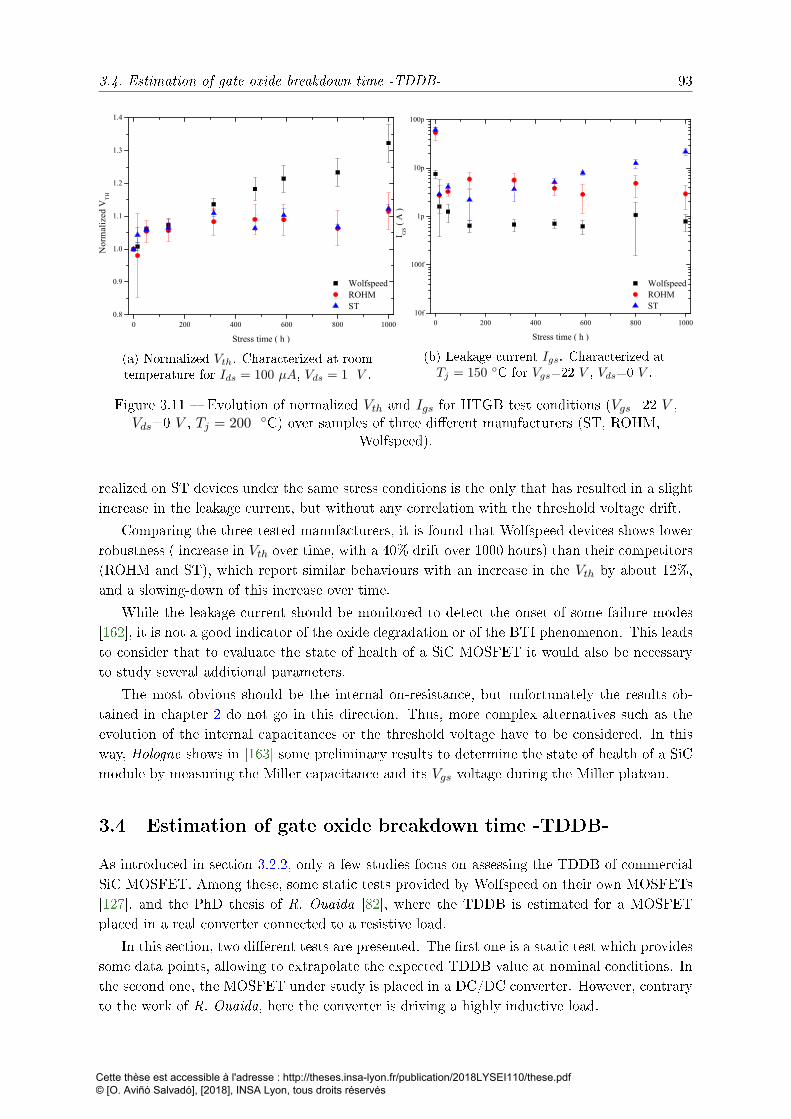
3.4. Estimation of gate oxide breakdown time -TDDB- 93
0 200 400 600 800 10000.8
0.9
1.0
1.1
1.2
1.3
1.4
Nor
mal
ized
pVT
H
Stressptimep(php)
WolfspeedROHMST
(a) Normalized Vth. Characterized at roomtemperature for Ids = 100 µA, Vds = 1 V .
0 200 400 600 800 100010f
100f
1p
10p
100p
I GS
( A
)
Stress time ( h )
WolfspeedROHMST
(b) Leakage current Igs. Characterized atTj = 150 C for Vgs=22 V , Vds=0 V .
Figure 3.11 Evolution of normalized Vth and Igs for HTGB test conditions (Vgs=22 V ,Vds=0 V , Tj = 200 C) over samples of three dierent manufacturers (ST, ROHM,
Wolfspeed).
realized on ST devices under the same stress conditions is the only that has resulted in a slightincrease in the leakage current, but without any correlation with the threshold voltage drift.
Comparing the three tested manufacturers, it is found that Wolfspeed devices shows lowerrobustness ( increase in Vth over time, with a 40% drift over 1000 hours) than their competitors(ROHM and ST), which report similar behaviours with an increase in the Vth by about 12%,and a slowing-down of this increase over time.
While the leakage current should be monitored to detect the onset of some failure modes[162], it is not a good indicator of the oxide degradation or of the BTI phenomenon. This leadsto consider that to evaluate the state of health of a SiC MOSFET it would also be necessaryto study several additional parameters.
The most obvious should be the internal on-resistance, but unfortunately the results ob-tained in chapter 2 do not go in this direction. Thus, more complex alternatives such as theevolution of the internal capacitances or the threshold voltage have to be considered. In thisway, Hologne shows in [163] some preliminary results to determine the state of health of a SiCmodule by measuring the Miller capacitance and its Vgs voltage during the Miller plateau.
3.4 Estimation of gate oxide breakdown time -TDDB-
As introduced in section 3.2.2, only a few studies focus on assessing the TDDB of commercialSiC MOSFET. Among these, some static tests provided by Wolfspeed on their own MOSFETs[127], and the PhD thesis of R. Ouaida [82], where the TDDB is estimated for a MOSFETplaced in a real converter connected to a resistive load.
In this section, two dierent tests are presented. The rst one is a static test which providessome data points, allowing to extrapolate the expected TDDB value at nominal conditions. Inthe second one, the MOSFET under study is placed in a DC/DC converter. However, contraryto the work of R. Ouaida, here the converter is driving a highly inductive load.
Cette thèse est accessible à l'adresse : http://theses.insa-lyon.fr/publication/2018LYSEI110/these.pdf © [O. Aviñó Salvadó], [2018], INSA Lyon, tous droits réservés
94 3. Robustness of the MOSFET gate oxide
To realize the extrapolation to nominal conditions, the electric eld is used as a accelerationfactor. The main models used in the literature are the thermochemical breakdown model [164]and the hole-induced breakdown model [165]. From both models, the most conservative is thethermochemical breakdown model. Indeed McPherson et al. showed that for a low electriceld the thermochemical model ts better [166]. Thus, the extrapolation to nominal conditionsis achieved using this latter model, which is described by eq. (3.1) and where tBD is the timebefore breakdown, A0 is a constant relative to the substrate, γ is the acceleration factor andEox the electric eld in the oxide.
tBD(Eox) = A0 · e−γ·Eox (3.1)
The devices under study are Wolfspeed C2M008012D SiC MOSFETs [152]. They are char-acterized (see annexe A.2) before the test, in order to verify that no DUT shows any anomaly.All the tests are run at Tj = 150 C.
The results obtained from the static test are compared to those obtained from the devicesplaced in a DC/DC converter, working under inductive switching conditions. The objective isto study if a major degradation of the MOSFET gate oxide can occur due to hard-switchingconditions.
The results of the static tests, which are shown in section 3.4.2.1, together with our desireto nd and indicator of the gate oxide health (as was discussed in sec. 3.3.3), lead us to analysethe degradation phenomena further. Some additional tests are run for a better understandingof the failure mechanisms, as well as to study if the internal capacitances could be used forhealth monitoring applications. These tests and their results are presented in sections 3.4.1.2and 3.4.2.2 respectively.
3.4.1 Experimental Methodology
The dierent tests described in sections 3.4.1.1 and 3.4.1.3 requires a previous characterizationof the leakage current Igs(Vgs). This allows to determine the voltage range where the Fowler-Nordheim injection phenomena is predominant, showing a linear behaviour in agreement withthe thermochemical model, which allows to extrapolate the obtained results to the nominalconditions of use.
The characterization of Igs requires some care: it is characterized at Tj = 150 C for 10dierent samples which had never been used before; using a Keithley SMU 2636B with triaxialconnections, and the device is placed in a metal enclosure to achieve good sensibility to lowcurrents (pA range). This is described in annex A.3 (see g. A.12).
The test conditions are: Vgs ramping from from 20 V to 50 V , with a compliance (maximumcurrent delivered by the source) of 100 mA. Very small steps are used (50 mV, with a delaybefore measurement of 1 second). These conditions are set using the control software embeddedin the instrument (TSP Express).
This setting allows to minimize the measurement of capacitive currents (ic) in agreementwith eq. (3.2), where the value of Cgs is extracted from de component's datasheet [152].
ic = Cgs ·dv
dt' 950 · 10−12 · 50 · 10−3
1= 47.5 pA (3.2)
Cette thèse est accessible à l'adresse : http://theses.insa-lyon.fr/publication/2018LYSEI110/these.pdf © [O. Aviñó Salvadó], [2018], INSA Lyon, tous droits réservés
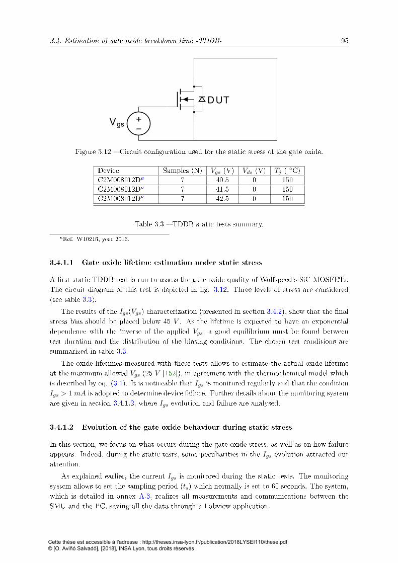
3.4. Estimation of gate oxide breakdown time -TDDB- 95
DUT
−+Vgs
Figure 3.12 Circuit conguration used for the static stress of the gate oxide.
Device Samples (N) Vgs (V) Vds (V) Tj ( C)C2M008012Da 7 40.5 0 150C2M008012Da 7 41.5 0 150C2M008012Da 7 42.5 0 150
Table 3.3 TDDB static tests summary.
aRef. W10216, year 2016.
3.4.1.1 Gate oxide lifetime estimation under static stress
A rst static TDDB test is run to assess the gate oxide quality of Wolfspeed's SiC MOSFETs.The circuit diagram of this test is depicted in g. 3.12. Three levels of stress are considered(see table 3.3).
The results of the Igs(Vgs) characterization (presented in section 3.4.2), show that the nalstress bias should be placed below 45 V . As the lifetime is expected to have an exponentialdependence with the inverse of the applied Vgs, a good equilibrium must be found betweentest duration and the distribution of the biasing conditions. The chosen test conditions aresummarized in table 3.3.
The oxide lifetimes measured with these tests allows to estimate the actual oxide lifetimeat the maximum allowed Vgs (25 V [152]), in agreement with the thermochemical model whichis described by eq. (3.1). It is noticeable that Igs is monitored regularly and that the conditionIgs > 1 mA is adopted to determine device failure. Further details about the monitoring systemare given in section 3.4.1.2, where Igs evolution and failure are analysed.
3.4.1.2 Evolution of the gate oxide behaviour during static stress
In this section, we focus on what occurs during the gate oxide stress, as well as on how failureappears. Indeed, during the static tests, some peculiarities in the Igs evolution attracted ourattention.
As explained earlier, the current Igs is monitored during the static tests. The monitoringsystem allows to set the sampling period (ts) which normally is set to 60 seconds. The system,which is detailed in annex A.3, realizes all measurements and communications between theSMU and the PC, saving all the data through a Labview application.
Cette thèse est accessible à l'adresse : http://theses.insa-lyon.fr/publication/2018LYSEI110/these.pdf © [O. Aviñó Salvadó], [2018], INSA Lyon, tous droits réservés
96 3. Robustness of the MOSFET gate oxide
Device Samples (N) Vgs (V) Vds (V) Tj ( C)C2M008012Da 1 41.5 0 150C2M008012Da 1 42 0 150C2M008012Da 1 42.5 0 150C2M008012Da 1 43 0 150C2M008012Da 1 43.5 0 150
Table 3.4 Tests realized to compare Igs evolution depending on the applied Vgs.
aRef. W10216, year 2016.
After the rst tests, an initial increase of the leakage current is observed. Thus, the Labviewprogramme is modied in order to incorporate the possibility to acquire data at a much higherrate. The objective is to study the initial behaviour of Igs.
To avoid bottleneck due to the communication between the PC and the SMU, the newroutine allows to program the SMU in order to perform rapid bursts of measurements (uptp ts=0.2 s in High-Accuracy acquisition mode [167]) saving the data into the internal SMUmemory. Once a determined number of measurements has been realized (about 1000 points),all measured data is sent to the PC. After that, the Labview program continues to measure thecurrent Igs, but with the slow mode where ts is setted to 60 s (as performing measurements athigh time rate would result in very large amount of data).
To study the evolution of Igs during the rst phases of the stress, ve devices are testedat dierent gate-source voltages. These tests are summarized in table 3.4. Moreover, as thesetests are run until the oxide failure, it is possible to observe how Igs evolves just before thefailure and therefore if any element could predict it.
The charge injected into the oxide is calculated using the trapezoidal integration methodwith the aim to verify if the dierent devices fails for a similar amount of injected charge. Eq.(3.3) is used to calculate the total injected charge at the time of failure (Qinjected), where N isthe total number of measurements before failure, and t is the stress time for each measurement.
Qinjected =
tfailure∫t=0
Igs(t) · dt ≈N∑k=1
Igs(k − 1) + Igs(k)
2· (tk − tk−1) (3.3)
An additional test is realized using a fresh device to analyse further the evolution of itscharacteristics during the static test stress. Thus, the DUT is characterized initially and thenrepetitively (9 times over 8 hours), tacking special care in the Vth and the gate input capacitanceCgs. As discussed in section 3.3, both parameters could be linked to a possible degradation ofthe dielectric. For further details about Cgs characterization, see Annex A.2.
Once the DUT has been characterized, it is stressed at Vgs=42.5 V for 15 minutes andcharacterized again. Successive stress stages (always at 42.5 V ) are realized, followed by char-acterization until the apparition of a dramatic failure in the oxide. The duration of the stressstages is increased gradually, because the main evolution of the parameters is observed duringthe rst hours of stress. The current Igs is monitored during all the test.
Cette thèse est accessible à l'adresse : http://theses.insa-lyon.fr/publication/2018LYSEI110/these.pdf © [O. Aviñó Salvadó], [2018], INSA Lyon, tous droits réservés
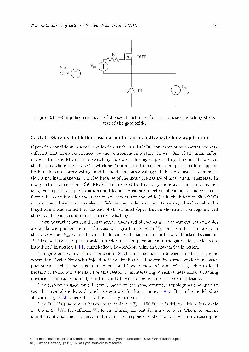
3.4. Estimation of gate oxide breakdown time -TDDB- 97
−+
540 V
Vdd
DUT
D1Isw
10 A
Vp1
R
Figure 3.13 Simplied schematic of the test-bench used for the inductive switching stresstest of the gate oxide.
3.4.1.3 Gate oxide lifetime estimation for an inductive switching application
Operation conditions in a real application, such as a DC/DC converter or an inverter are verydierent that those experienced by the component in a static stress. One of the main dier-ences is that the MOSFET is switching its state, allowing or preventing the current ow. Atthe instant where the device is switching from a state to another, some perturbations appear,both in the gate-source voltage and in the drain-source voltage. This is because the commuta-tion is not instantaneous, but also because of the inductive nature of most circuit elements. Inmany actual applications, SiC MOSFETs are used to drive very inductive loads, such as mo-tors, causing greater perturbations and favouring carrier injection phenomena. Indeed, mostfavourable conditions for the injection of carriers into the oxide (or in the interface SiC/SiO2)occurs when there is a cross electric eld in the oxide, a current traversing the channel and alongitudinal electric eld at the end of the channel (operating in the saturation region). Allthese conditions occurs in an inductive switching.
These perturbations could cause several undesired phenomena. The most evident examplesare avalanche phenomenon in the case of a great increase in Vds, or a short-circuit event inthe case where Vgs would become high enough to turn-on an otherwise blocked transistor.Besides, both types of perturbations carrier injection phenomena in the gate oxide, which wereintroduced in section 1.4.1; tunnel-eect, Fowler-Nordheim and hot-carrier injection.
The gate bias values selected in section 3.4.1.1 for the static tests corresponds to the zonewhere the Fowler-Nordheim injection is predominant. However, in a real application, otherphenomena such as hot-carrier injection could have a more relevant role (e.g. due to localheating or to inductive loads). For this reason, it is interesting to realize tests under switchingoperation conditions to analyse if this could have a repercussion on the oxide lifetime.
The test-bench used for this test is based on the same converter topology as that used totest the internal diode, and which is described further in annexe A.5. It can be modelled asshown in g. 3.13, where the DUT is the high-side switch.
The DUT is placed on a hot-plate to achieve a Tj = 150 C. It is driven with a duty cycleD=0.5 at 20 kHz for dierent Vgs levels. During the test Ids is set to 10 A. The gate currentis not monitored, and the measured lifetime corresponds to the moment when a catastrophic
Cette thèse est accessible à l'adresse : http://theses.insa-lyon.fr/publication/2018LYSEI110/these.pdf © [O. Aviñó Salvadó], [2018], INSA Lyon, tous droits réservés
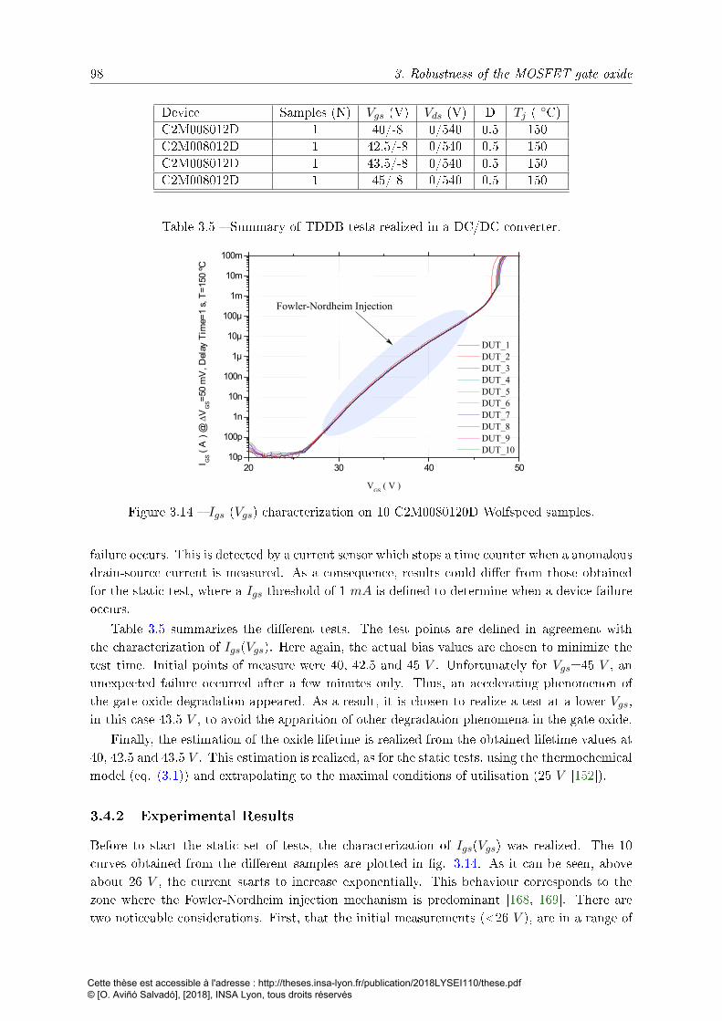
98 3. Robustness of the MOSFET gate oxide
Device Samples (N) Vgs (V) Vds (V) D Tj ( C)C2M008012D 1 40/-8 0/540 0.5 150C2M008012D 1 42.5/-8 0/540 0.5 150C2M008012D 1 43.5/-8 0/540 0.5 150C2M008012D 1 45/-8 0/540 0.5 150
Table 3.5 Summary of TDDB tests realized in a DC/DC converter.
20 30 40 5010p
100p
1n
10n
100n
1µ
10µ
100µ
1m
10m
100m
I GS
( A
) @
∆V
GS=
50 m
V, D
elay
Tim
e=1
s, T
=15
0 ºC
VGS
(5V5)
DUT_1DUT_2DUT_3DUT_4DUT_5DUT_6DUT_7DUT_8DUT_9DUT_10
Fowler-Nordheim5Injection
Figure 3.14 Igs (Vgs) characterization on 10 C2M0080120D Wolfspeed samples.
failure occurs. This is detected by a current sensor which stops a time counter when a anomalousdrain-source current is measured. As a consequence, results could dier from those obtainedfor the static test, where a Igs threshold of 1 mA is dened to determine when a device failureoccurs.
Table 3.5 summarizes the dierent tests. The test points are dened in agreement withthe characterization of Igs(Vgs). Here again, the actual bias values are chosen to minimize thetest time. Initial points of measure were 40, 42.5 and 45 V . Unfortunately for Vgs=45 V , anunexpected failure occurred after a few minutes only. Thus, an accelerating phenomenon ofthe gate oxide degradation appeared. As a result, it is chosen to realize a test at a lower Vgs,in this case 43.5 V , to avoid the apparition of other degradation phenomena in the gate oxide.
Finally, the estimation of the oxide lifetime is realized from the obtained lifetime values at40, 42.5 and 43.5 V . This estimation is realized, as for the static tests, using the thermochemicalmodel (eq. (3.1)) and extrapolating to the maximal conditions of utilisation (25 V [152]).
3.4.2 Experimental Results
Before to start the static set of tests, the characterization of Igs(Vgs) was realized. The 10curves obtained from the dierent samples are plotted in g. 3.14. As it can be seen, aboveabout 26 V , the current starts to increase exponentially. This behaviour corresponds to thezone where the Fowler-Nordheim injection mechanism is predominant [168, 169]. There aretwo noticeable considerations. First, that the initial measurements (<26 V ), are in a range of
Cette thèse est accessible à l'adresse : http://theses.insa-lyon.fr/publication/2018LYSEI110/these.pdf © [O. Aviñó Salvadó], [2018], INSA Lyon, tous droits réservés
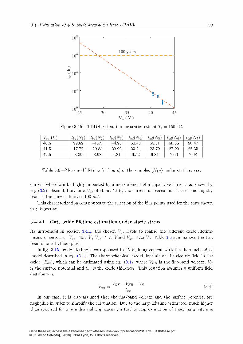
3.4. Estimation of gate oxide breakdown time -TDDB- 99
Vgs ( V )25 30 35 40 45
t bd
( h
)
100
102
104
106
108
100 years
Figure 3.15 TDDB estimation for static tests at Tj = 150 C.
Vgs (V) tbd(N1) tbd(N2) tbd(N3) tbd(N4) tbd(N5) tbd(N6) tbd(N7)
40.5 29.62 41.59 44.28 50.43 55.81 56.36 56.4741.5 17.72 20.85 22.96 23.24 23.79 27.92 28.3542.5 3.09 3.98 4.31 6.52 6.81 7.06 7.98
Table 3.6 Measured lifetime (in hours) of the samples (N1:7) under static stress.
current where can be highly impacted by a measurement of a capacitive current, as shown byeq. (3.2). Second, that for a Vgs of about 46 V , the current increases much faster and rapidlyreaches the current limit of 100 mA.
This characterization contributes to the selection of the bias points used for the tests shownin this section.
3.4.2.1 Gate oxide lifetime estimation under static stress
As introduced in section 3.4.1, the chosen Vgs levels to realize the dierent oxide lifetimemeasurements are: Vgs=40.5 V , Vgs=41.5 V and Vgs=42.5 V . Table 3.6 summarizes the testresults for all 21 samples.
In g. 3.15, oxide lifetime is extrapolated to 25 V , in agreement with the thermochemicalmodel described in eq. (3.1). The thermochemical model depends on the electric eld in theoxide (Eox), which can be estimated using eq. (3.4), where VFB is the at-band voltage, VSis the surface potential and tox is the oxide thickness. This equation assumes a uniform elddistribution.
Eox ≈VGS − VFB − VS
tox(3.4)
In our case, it is also assumed that the at-band voltage and the surface potential arenegligible in order to simplify the calculation. Due to the large lifetime estimated, much higherthan required for any industrial application, a further approximation of these parameters is
Cette thèse est accessible à l'adresse : http://theses.insa-lyon.fr/publication/2018LYSEI110/these.pdf © [O. Aviñó Salvadó], [2018], INSA Lyon, tous droits réservés
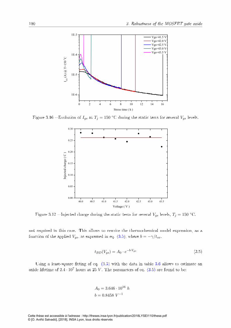
100 3. Robustness of the MOSFET gate oxide
0 2 4 6 8 10 12 14 16
1E-6
1E-5
1E-4
1E-3
I GS
(A).
@.T
=15
0.o C
.
Stress.time.(.h.)
Vgs=41.5.VVgs=42.0.VVgs=42.5.VVgs=43.0.VVgs=43.5.V
Figure 3.16 Evolution of Igs at Tj = 150 C during the static tests for several Vgs levels.
40.0 40.5 41.0 41.5 42.0 42.5 43.0 43.50.00
0.05
0.10
0.15
0.20
0.25
0.30
Inje
cted
cha
rge
( C
)
Voltage ( V )
Figure 3.17 Injected charge during the static tests for several Vgs levels, Tj = 150 C.
not required in this case. This allows to rewrite the thermochemical model expression, as afunction of the applied Vgs, as expressed in eq. (3.5), where b = −γ/tox.
tBD(Vgs) = A0 · e−b·Vgs (3.5)
Using a least-square tting of eq. (3.5) with the data in table 3.6 allows to estimate anoxide lifetime of 2.4 · 107 hours at 25 V . The parameters of eq. (3.5) are found to be:
A0 = 3.646 · 1016 h
b = 0.8458 V −1
Cette thèse est accessible à l'adresse : http://theses.insa-lyon.fr/publication/2018LYSEI110/these.pdf © [O. Aviñó Salvadó], [2018], INSA Lyon, tous droits réservés
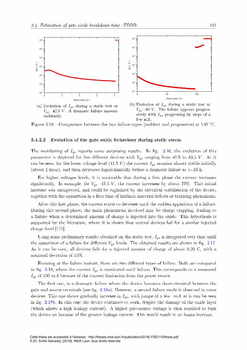
3.4. Estimation of gate oxide breakdown time -TDDB- 101
0 2 4 6 810-7
10-6
10-5
10-4
10-3
10-2
10-1
Igs
( A
)
Stress time ( h )
(a) Evolution of Igs during a static test atVgs=42.5 V . A dramatic failure appearssuddently.
0 50 10010-7
10-6
10-5
10-4
10-3
10-2
10-1
Igs
( A
)
Stress time ( h )
(b) Evolution of Igs during a static test atVgs=40 V . The failure appears progres-sively with Igs progressing by steps of afew mA.
Figure 3.18 Comparison between the two failure types (suddent and progressive) at 150 C.
3.4.2.2 Evolution of the gate oxide behaviour during static stress
The monitoring of Igs reports some surprising results. In g. 3.16, the evolution of thisparameter is depicted for ve dierent devices with Vgs ranging from 41.5 to 43.5 V . As itcan be seen, for the lower voltage level (41.5 V ) the current Igs remains almost stable initially(about 1 hour), and then decreases logarithmically before a dramatic failure at t=16 h.
For higher voltages levels, it is noticeable that during a rst phase the current increasessignicantly. In example, for Vgs=43.5 V , the current increases by about 70%. This initialincrease was unexpected, and could be explained by the electrical stabilisation of the device,together with the apparition in a rst time of intrinsic material defects or trapping phenomena.
After this rst phase, the current starts to decrease until the sudden apparition of a failure.During this second phase, the main phenomena involved may be charge trapping, leading toa failure when a determined amount of charge is injected into the oxide. This hypothesis issupported by the literature, where it is shown that several devices fail for a similar injectedcharge level [170].
Using some preliminary results obtained on the static test, Igs is integrated over time untilthe apparition of a failure for dierent Vgs levels. The obtained results are shown in g. 3.17.As it can be seen, all devices fails for a injected amount of charge of about 0.26 C, with amaximal deviation of 15%.
Focusing at the failure instant, there are two dierent types of failure. Both are comparedin g. 3.18, where the current Igs is monitored until failure. This corresponds to a measuredIgs of 100 mA because of the current limitation from the power source.
The rst one, is a dramatic failure where the device becomes short-circuited between thegate and source terminals (see g. 3.18a). However, a second failure mode is observed in somedevices. This one shows gradually increase in Igs, with jumps of a few mA as it can be seenin g. 3.18b. In this case the device continues to work, despite the damage of the oxide layer(which allows a high leakage current). A higher gate-source voltage is then required to turnthe device on because of the greater leakage current. This would result in an losses increase.
Cette thèse est accessible à l'adresse : http://theses.insa-lyon.fr/publication/2018LYSEI110/these.pdf © [O. Aviñó Salvadó], [2018], INSA Lyon, tous droits réservés
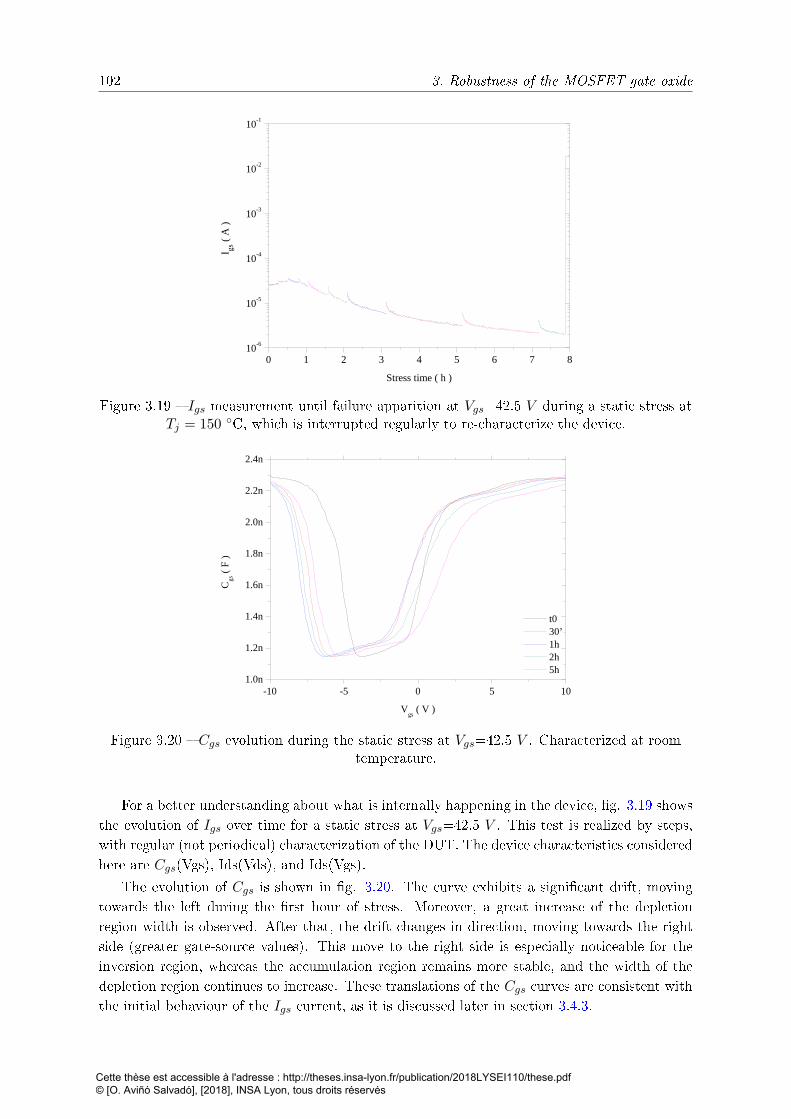
102 3. Robustness of the MOSFET gate oxide
0 1 2 3 4 5 6 7 81 0 - 6
1 0 - 5
1 0 - 4
1 0 - 3
1 0 - 2
1 0 - 1
I gs ( A )
S t r e s s t i m e ( h )
Figure 3.19 Igs measurement until failure apparition at Vgs=42.5 V during a static stress atTj = 150 C, which is interrupted regularly to re-characterize the device.
- 1 0 - 5 0 5 1 01 . 0 n
1 . 2 n
1 . 4 n
1 . 6 n
1 . 8 n
2 . 0 n
2 . 2 n
2 . 4 n
C gs ( F )
V g s ( V )
t 0 3 0 ' 1 h 2 h 5 h
Figure 3.20 Cgs evolution during the static stress at Vgs=42.5 V . Characterized at roomtemperature.
For a better understanding about what is internally happening in the device, g. 3.19 showsthe evolution of Igs over time for a static stress at Vgs=42.5 V . This test is realized by steps,with regular (not periodical) characterization of the DUT. The device characteristics consideredhere are Cgs(Vgs), Ids(Vds), and Ids(Vgs).
The evolution of Cgs is shown in g. 3.20. The curve exhibits a signicant drift, movingtowards the left during the rst hour of stress. Moreover, a great increase of the depletionregion width is observed. After that, the drift changes in direction, moving towards the rightside (greater gate-source values). This move to the right side is especially noticeable for theinversion region, whereas the accumulation region remains more stable, and the width of thedepletion region continues to increase. These translations of the Cgs curves are consistent withthe initial behaviour of the Igs current, as it is discussed later in section 3.4.3.
Cette thèse est accessible à l'adresse : http://theses.insa-lyon.fr/publication/2018LYSEI110/these.pdf © [O. Aviñó Salvadó], [2018], INSA Lyon, tous droits réservés
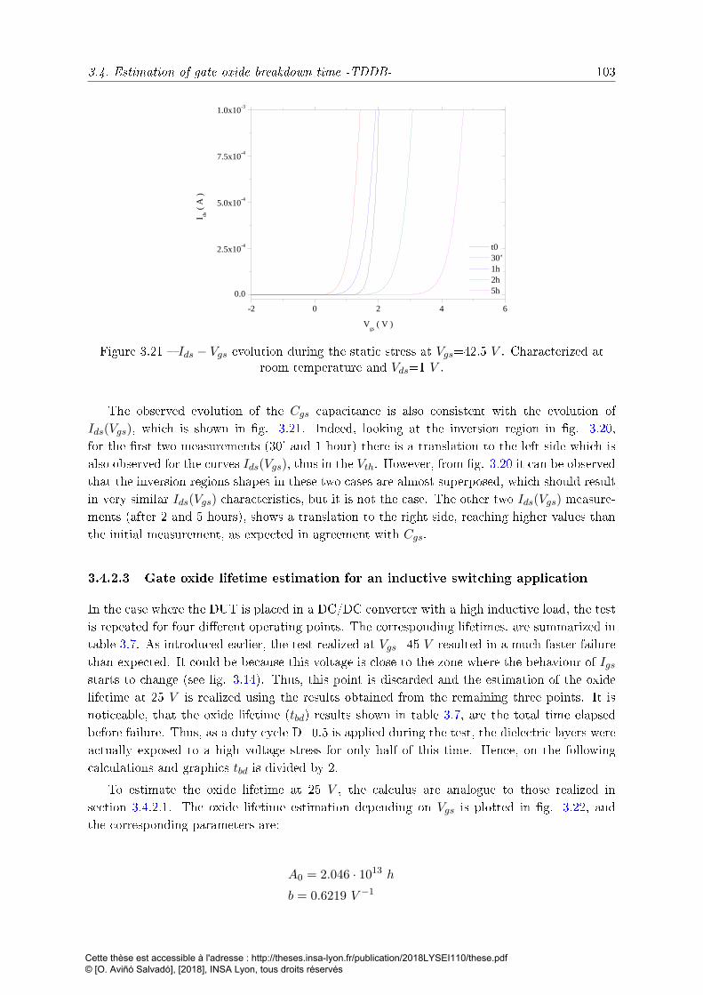
3.4. Estimation of gate oxide breakdown time -TDDB- 103
- 2 0 2 4 60 . 0
2 . 5 x 1 0 - 4
5 . 0 x 1 0 - 4
7 . 5 x 1 0 - 4
1 . 0 x 1 0 - 3
I ds ( A )
V g s ( V )
t 0 3 0 ' 1 h 2 h 5 h
Figure 3.21 Ids − Vgs evolution during the static stress at Vgs=42.5 V . Characterized atroom temperature and Vds=1 V .
The observed evolution of the Cgs capacitance is also consistent with the evolution ofIds(Vgs), which is shown in g. 3.21. Indeed, looking at the inversion region in g. 3.20,for the rst two measurements (30' and 1 hour) there is a translation to the left side which isalso observed for the curves Ids(Vgs), thus in the Vth. However, from g. 3.20 it can be observedthat the inversion regions shapes in these two cases are almost superposed, which should resultin very similar Ids(Vgs) characteristics, but it is not the case. The other two Ids(Vgs) measure-ments (after 2 and 5 hours), shows a translation to the right side, reaching higher values thanthe initial measurement, as expected in agreement with Cgs.
3.4.2.3 Gate oxide lifetime estimation for an inductive switching application
In the case where the DUT is placed in a DC/DC converter with a high inductive load, the testis repeated for four dierent operating points. The corresponding lifetimes, are summarized intable 3.7. As introduced earlier, the test realized at Vgs=45 V resulted in a much faster failurethan expected. It could be because this voltage is close to the zone where the behaviour of Igsstarts to change (see g. 3.14). Thus, this point is discarded and the estimation of the oxidelifetime at 25 V is realized using the results obtained from the remaining three points. It isnoticeable, that the oxide lifetime (tbd) results shown in table 3.7, are the total time elapsedbefore failure. Thus, as a duty cycle D=0.5 is applied during the test, the dielectric layers wereactually exposed to a high voltage stress for only half of this time. Hence, on the followingcalculations and graphics tbd is divided by 2.
To estimate the oxide lifetime at 25 V , the calculus are analogue to those realized insection 3.4.2.1. The oxide lifetime estimation depending on Vgs is plotted in g. 3.22, andthe corresponding parameters are:
A0 = 2.046 · 1013 h
b = 0.6219 V −1
Cette thèse est accessible à l'adresse : http://theses.insa-lyon.fr/publication/2018LYSEI110/these.pdf © [O. Aviñó Salvadó], [2018], INSA Lyon, tous droits réservés
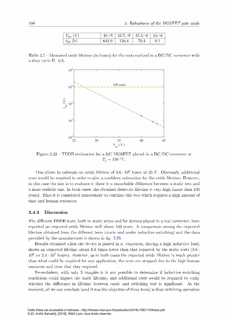
104 3. Robustness of the MOSFET gate oxide
Vgs (V) 40/-8 42.5/-8 43.5/-8 45/-8tbd (h) 642.8 130.8 79.4 0.1
Table 3.7 Measured oxide lifetime (in hours) for the tests realized in a DC/DC converter witha duty cycle D=0.5.
Vgs
( V )25 30 35 40 45
t bd(
h )
100
102
104
106
108
100 years
Figure 3.22 TDDB estimation for a SiC MOSFET placed in a DC/DC converter atTj = 150 C.
This allows to estimate an oxide lifetime of 3.6 · 106 hours at 25 V . Obviously, additionaltests would be required in order to give a condent estimation for the oxide lifetime. However,in this case the aim is to evaluate it there is a remarkable dierence between a static test anda more realistic one. In both cases, the obtained dielectric lifetime is very high (more than 100years). Thus it is considered unnecessary to continue this test which requires a high amount oftime and human resources.
3.4.3 Discussion
The dierent TDDB tests, both in static stress and for devices placed in a real converter, havereported an expected oxide lifetime well above 100 years. A comparison among the expectedlifetime obtained from the dierent tests (static and under inductive switching) and the dataprovided by the manufacturer is shown in g. 3.23.
Results obtained when the device is placed in a converter, driving a high inductive load,shows an expected lifetime about 6.6 times lower than that reported by the static tests (3.6 ·106 vs 2.4 · 107 hours). However, as in both cases the expected oxide lifetime is much greaterthan what could be required for any application, the tests are stopped due to the high humanresources and time that they required.
Nevertheless, with only 3 samples it is not possible to determine if inductive switchingconditions could impact the oxide lifetime, and additional tests would be required to verifywhether the dierence in lifetime between static and switching test is signicant. At themoment, all we can conclude (and it was the objective of these tests) is that switching operation
Cette thèse est accessible à l'adresse : http://theses.insa-lyon.fr/publication/2018LYSEI110/these.pdf © [O. Aviñó Salvadó], [2018], INSA Lyon, tous droits réservés
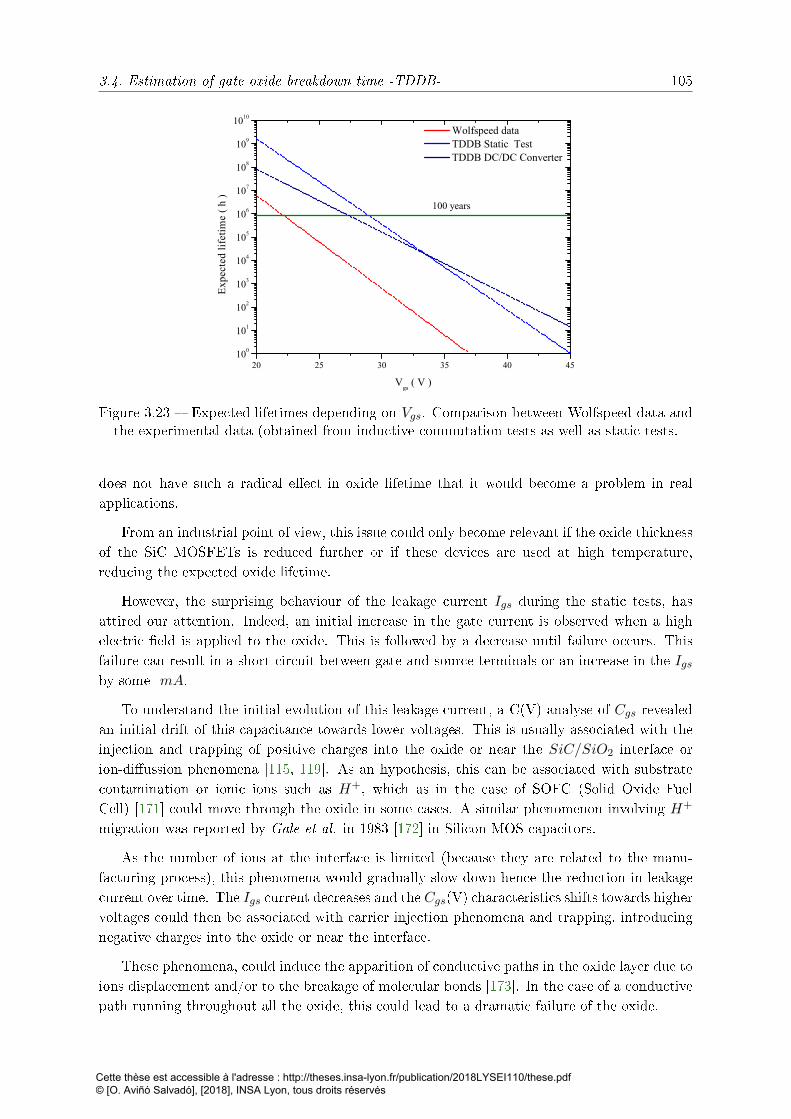
3.4. Estimation of gate oxide breakdown time -TDDB- 105
20 25 30 35 40 45100
101
102
103
104
105
106
107
108
109
1010
Exp
ecte
dTli
feti
meT
rThT
y
Vgs
rTVTy
WolfspeedTdataTDDBTStaticT TestTDDBTDC/DCTConverter
100Tyears
Figure 3.23 Expected lifetimes depending on Vgs. Comparison between Wolfspeed data andthe experimental data (obtained from inductive commutation tests as well as static tests.
does not have such a radical eect in oxide lifetime that it would become a problem in realapplications.
From an industrial point of view, this issue could only become relevant if the oxide thicknessof the SiC MOSFETs is reduced further or if these devices are used at high temperature,reducing the expected oxide lifetime.
However, the surprising behaviour of the leakage current Igs during the static tests, hasattired our attention. Indeed, an initial increase in the gate current is observed when a highelectric eld is applied to the oxide. This is followed by a decrease until failure occurs. Thisfailure can result in a short-circuit between gate and source terminals or an increase in the Igsby some mA.
To understand the initial evolution of this leakage current, a C(V) analyse of Cgs revealedan initial drift of this capacitance towards lower voltages. This is usually associated with theinjection and trapping of positive charges into the oxide or near the SiC/SiO2 interface orion-diussion phenomena [115, 119]. As an hypothesis, this can be associated with substratecontamination or ionic ions such as H+, which as in the case of SOFC (Solid Oxide FuelCell) [171] could move through the oxide in some cases. A similar phenomenon involving H+
migration was reported by Gale et al. in 1983 [172] in Silicon MOS capacitors.
As the number of ions at the interface is limited (because they are related to the manu-facturing process), this phenomena would gradually slow down hence the reduction in leakagecurrent over time. The Igs current decreases and the Cgs(V) characteristics shifts towards highervoltages could then be associated with carrier injection phenomena and trapping, introducingnegative charges into the oxide or near the interface.
These phenomena, could induce the apparition of conductive paths in the oxide layer due toions displacement and/or to the breakage of molecular bonds [173]. In the case of a conductivepath running throughout all the oxide, this could lead to a dramatic failure of the oxide.
Cette thèse est accessible à l'adresse : http://theses.insa-lyon.fr/publication/2018LYSEI110/these.pdf © [O. Aviñó Salvadó], [2018], INSA Lyon, tous droits réservés
106 3. Robustness of the MOSFET gate oxide
3.5 Conclusions
The objective of this chapter is the study the robustness of the gate dielectric (SiO2) and toverify if its expected lifetime is in agreement with the industry requirements. The study isfocused on two main measurements of the gate oxide degradation: BTI and TDDB.
For BTI, it has been veried in agreement with [160], that the most stressful conguration iswhen drain and source terminals are short-circuited, and a positive Vgs (close to the maximumvalue) is applied. This conguration corresponds to the classic HTGB test. For this case, rstsBTIs appears at about 170-180 C (for Vgs=22 V ).
Tests realized on Wolfspeed MOSFETs at 150 C have shown no signicant BTIs over 1000hours of stress, with a maximal increase in the Vth of 5%. However, the tests realized at 200 C(Vgs=22 V ), have shown a great increase in the Vth. In both cases, the Igs current remainedstable. Thus, it is not a good indicator of BTIs, even if its monitoring could be requiredregarding other undesired phenomena such as short-circuit [162].
Finally, regarding BTIs, it is noticeable that Wolfspeed MOSFETs are found to be the mostsensitive to this phenomena, whereas ROHM and ST SiC MOSFETs do not show a signicantdegradation, with a Vth increase of about 12% over 1000 hours, without showing a clear tend.As for Wolfspeed MOSFETs, the leakage Igs current has not been found to be an indicativeparameter of the oxide degradation.
With TDDB tests, the expected oxide lifetime has been found to be well above 100 years inthe two cases under study: under static stress (3.6 · 106 hours )and when the device is placedin a real converter driving an inductive load (2.4 · 107 hours). In this latter case, only threesamples have been stressed. While this small sample size is too small to allow for an accuratecomparison with the static tests, it is sucient to demonstrate that oxide lifetime should notbe an issue in real operating cases.
The most signicant issue related to the TDDB is the observed mode of failure, wherethe current Igs shows a great increase, leading to a dramatic failure (gate-source short-circuit)or increasing to some mA. In this last case, the device is still capable to work, even if theloses should increase notably. Regarding the behaviour of Igs and the capacitance Cgs, ourconclusion is that during the tests two phenomena are involved. A rst one which would bepredominant at the beginning (at least when high electric eld is applied to the oxide) movingpositive charges into the oxide or in the interface. This phenomena could be related to thepresence of contamination or ionic ions, such as H+. After that, another phenomena becomespredominant, moving negative charges into/near the oxide. This phenomena might be relatedto carrier injection and trapping.
It is concluded that the SiC MOSFETs show a good robustness of the gate oxide, allowingtheir use for industrial applications at temperatures of Tj = 150 C. Nevertheless, beforeexploring their use in high temperature applications, some issues should be addressed. Thisis the case of BTI apparition for temperatures above 170 C (Wolfspeed) or the presence ofmobile ions in/near the interface. These two issues are probably related.
Cette thèse est accessible à l'adresse : http://theses.insa-lyon.fr/publication/2018LYSEI110/these.pdf © [O. Aviñó Salvadó], [2018], INSA Lyon, tous droits réservés

Conclusions
In this thesis, the main robustness issues concerning SiC MOSFETs have been studied. Con-trary to some years ago, where the main problems concerned SiC epitaxy, today the main issuesfocus on device characteristics and their robustness in dierent operation modes.
In this thesis, two dierent issues have been addressed on 1200 V SiC MOSFETs:
Intrinsic diode degradation, which may be due to the presence of SFs inducing a shift ofthe diode forward voltage (Vf ).
Gate oxide reliability, which can be divided in two dierent aspects:
1. Oxide or dielectric expected lifetime (estimated by TDDB test).
2. Threshold voltage (Vth) drift (evaluated by BTI tests).
Other aspects concerning the robustness of SiC MOSFETs are linked to the operation modeof the devices, such as the occurrence of short-circuit or avalanche events. These issues are notbeen addressed in this thesis because they were studied in the same project by a complementarythesis [133].
The robustness of the intrinsic diode has been addressed in chapter 2 with the objective tovalidate if SiC MOSFETs could be used for diode-less applications (e.g. in an inverter). In thiskind of applications, the internal diode is typically solicited during the dead-times. In this way,tests have been addressed in static mode, but also placing the DUT in an inductive switchingconverter (which are the most stressful conditions of operation).
In both cases, no signicant drift of the Vf has been observed. This matches with recentpublications of the manufacturers indicating an important reduction of the SFs and BDP defectsin the substrates [158, 159].
However, with a current stress of the internal diode, an important Vth drift appears insome cases. This could probably be related to carrier injection phenomena and trapping at theSiO2/SiC interface, or in the oxide. This drift of the Vth appears in both modes of operation(static and in a converter). Moreover, for the same gate-source voltage (i.e. Vgs = −8 V ), thisdrift is very similar in both cases. For lower gate-source potentials, the Vth drift is drasticallyminimized (i.e. Vgs = −5 V ). Thus, this Vth drift depends of the applied gate-source potential,or as some tests introduced, on the duty cycle (by de-trapping phenomenon).
Complementary tests, stressing the channel instead of the body diode for Vgs = 20 V thesame temperature (150 C) and dissipated power than for the third quadrant tests, does notresults in signicant Vth drift.
Cette thèse est accessible à l'adresse : http://theses.insa-lyon.fr/publication/2018LYSEI110/these.pdf © [O. Aviñó Salvadó], [2018], INSA Lyon, tous droits réservés
108 Conclusions
Thus, a signicant Vth drift only appears (at 150 C) in the case where the P-N junction isstressed (in HTGB tests, a Vth drift is observed at higher temperatures). Then, the accumula-tion regime could favour this degradation of the Vth (only observed for Wolfspeed devices).
To observe a Vth drift (at 150 C), even in accumulation regime, a stress of the P-N junctionis required. An hypothesis that we can formulate is that due to the signicant amount of powerdissipated in the device during the test, an important temperature gradient appears betweenthe drift region an the top of the device, favouring hole injection in the oxide or near theinterface SiC/SiO2 and resulting in a Vth drift. To validate this hypothesis, thermal andelectric simulations of the device are required.
It is necessary to note that these results are obtained for Wolfspeed MOSFETs. ST andROHM devices have also been also tested (only placed in the converter test-bench). Devicesfrom these manufacturers do not exhibit any signicant degradation of the Vf , nor in the Vthfor the same conditions of operation.
Thus, the utilisation of the internal diode for diode-less applications is possible with theactual technology. In the case of Wolfspeed SiC MOSFETs, it should be possible taking someprecautions regarding the Vth drift and spurious turn-on of the device. Indeed, even if WolfspeedMOSFETs show a signicant drift of the Vth in some tests, in a real application the P-N junctionis only solicited during a small fraction of the overall period. This fact, together with the slightdrift observed in more realistic cases (0.05 < duty cycle < 0.85) seem to validate their utilisationfor industrial applications.
Regarding gate oxide robustness, the dierent test realized in chapter 3 indicate that ex-pected lifetime (TDDB measurement) is no longer a main issue for SiC MOSFETs. TDDBmeasurements are realised. One in static mode, applying a gate-source voltage high enough toaccelerate the oxide degradations. Another one, placing the devices in a real converter to stressfurther the device. The obtained oxide lifetime from our tests is higher than that providedby the manufacturer (x10) [161], which assures 10 years at 25 V , and well above 100 years atVgs = 20 V , which is the recommended Vgs.
BTIs probably remains as main robustness issue for SiC MOSFETs. HTGB test in Wolf-speed MOSFETs resulted in the apparition of Vth drift after some hours about 170-180 C andVgs=22 V . This instability is not signicant for ROHM and ST MOSFETs, even at 200 C.Contrary what we expected, Igs current is not found to be an indicative parameter of this Vthdrift, as measurement results in similar values during overall the test, whereas the Vth drift(positive) could be about 30% after 1000 hours (test conditions Vgs=22 V at 200 C).
With the aim to evaluate the behaviour of the oxide and trapping injection phenomenawhich may occur, the Igs current has been monitored during some TDDB tests. From thesetests we observed two surprising phenomena.
1. A great and progressive increase of the Igs current during the rst minutes of the TDDBtest.
2. In some cases, device resulted in partial failure(s), with currents around some mA andincreasing progressively by current steps.
With a further study, stopping TDDB test and characterizing the gate-source capacitanceregularly, it is observed that the C(V) characteristics shift to the left side during the phasewhere the Igs current increases and to the right side when it starts to decrease. An hypothesis
Cette thèse est accessible à l'adresse : http://theses.insa-lyon.fr/publication/2018LYSEI110/these.pdf © [O. Aviñó Salvadó], [2018], INSA Lyon, tous droits réservés
Conclusions 109
that could explain this phenomena is that the injection of positive charges in the oxide or in theinterface during a rst time. These positive charges could be mobile ions such as H+. As thenumber of this type of charges is limited (they are associated to the manufacturing process),once they are moved the current starts to decrease (as initially expected). In this second time,the main phenomena may be associated to carrier injection electrons and trapping.
In the case that ions would diuse into the oxide, due to their size it could result in a greatincrease of the leakage current (as leakage current steps observed during the tests). However,it is not possible to explain if these current steps should be related to a perforation through allthe oxide layer, which becomes larger, or perhaps to multiples and locate degradations of theoxide resulting in a local thinner layer.
Regarding industrial applications, gate robustness is no longer an impediment. The onlydegradations observed in this thesis regards Wolfspeed MOSFETs operating well above 150 C.ST and ROHM MOSFETs do not shows important Vth drifts (about 12% at 200 C over 1000hours). However, it seems obvious that before to explore the use of SiC MOSFETs in hightemperature applications, further studies should be carried out.
In GENOME project, it has also been studied by M. Cheng [133] the robustness of SiCMOSFETs under short-circuit and/or avalanche conditions. It is concluded that SiC MOSFETsare very vulnerable in these operation modes. Thus, it is required to evaluate if the protectionsystems used until now for silicon MOSFETs are adapted to SiC devices or if it is required toredesign them for a faster protection.
Cette thèse est accessible à l'adresse : http://theses.insa-lyon.fr/publication/2018LYSEI110/these.pdf © [O. Aviñó Salvadó], [2018], INSA Lyon, tous droits réservés

Cette thèse est accessible à l'adresse : http://theses.insa-lyon.fr/publication/2018LYSEI110/these.pdf © [O. Aviñó Salvadó], [2018], INSA Lyon, tous droits réservés
Future Work
As the results obtained in this thesis highlight that the robustness issues regarding the internaldiode have been overcome, future work should focus in the gate oxide robustness. The mainissues for power electronics applications are the following:
Apparition of BTI during forward current stress of the intrinsic diode. Thistype of degradation requires some complementary investigations and tests. This involvesdeveloping a thermal and electrical model of the device to evaluate the apparition oftemperature gradients during a stress of the internal diode. Some tests should quicklyindicate if this Vth drift is associated with the apparition of temperature gradients in thedevice structure. Among them, tests stressing the internal diode at dierent currentslevels and temperatures, and eventually a set of tests applying dierent duty cycles in thecase of CMB tests (a larger experiment set). To study this issue further, the identicationof the defects causing this degradation of the Vth could be studied by techniques such asDLTS and reproduced by simulation tools.
BTIs at higher temperatures. This requires, as above, the improvement of the gateoxide quality and of the SiC/SiO2 interface. HTGB test will continue to be required toevaluate the new generation of devices for temperatures above 200 C. Today (as reportedin this thesis), 1200 V MOSFETs can operate without the apparition2 of signicantinstabilities in the threshold voltage up to 170 C.
Evaluation of the impact of short-circuit and avalanche events in the expected
lifetime. In this thesis, the TDDB tests resulted in great expected lifetime for 1200 VSiC devices (>100 years; in static mode, or under conditions of inductive switching).However, the apparition of some operation modes such as short-circuit or avalanche is verystressful for the devices because of the high power dissipated, causing great temperatureincrease in the device and accelerating their degradation. Many applications incorporateprotection systems for these operation modes, but they are based on the "know-how"accumulated from silicon devices. Thus, TDDB tests should be carried on SiC devicesstressed repetitively in these modes of operation. Results should be compared with theduration of the stress events, in order to evaluate the corresponding gate oxide degradationand to supply data for the design of protection systems.
2Except for the case where the internal diode is stressed.
Cette thèse est accessible à l'adresse : http://theses.insa-lyon.fr/publication/2018LYSEI110/these.pdf © [O. Aviñó Salvadó], [2018], INSA Lyon, tous droits réservés

Cette thèse est accessible à l'adresse : http://theses.insa-lyon.fr/publication/2018LYSEI110/these.pdf © [O. Aviñó Salvadó], [2018], INSA Lyon, tous droits réservés
Appendix A
ANNEXES
Contents
A.1 Main Bias Tests . . . . . . . . . . . . . . . . . . . . . . . . . . . . . . 114
A.2 Device Characterization . . . . . . . . . . . . . . . . . . . . . . . 116
A.3 Measurement of the leakage current Igs . . . . . . . . . . 122
A.4 Estimation of the junction temperature . . . . . . . . . . . 125
A.5 CMB Test-Bench Description . . . . . . . . . . . . . . . . . . . 131
A.6 Internal diode robustness data . . . . . . . . . . . . . . . . . . 137
Cette thèse est accessible à l'adresse : http://theses.insa-lyon.fr/publication/2018LYSEI110/these.pdf © [O. Aviñó Salvadó], [2018], INSA Lyon, tous droits réservés
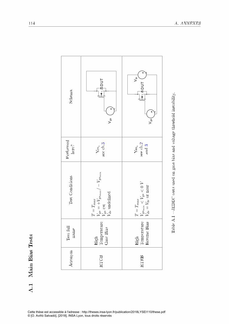
114 A. ANNEXES
A.1
Main
BiasTests
Acronym
Testfull
name
TestConditions
Perform
edhere?
Schema
HTGB
High
Tem
perature
GateBias
T=Tmax
Vgs
=+Vgs m
ax/−Vgs m
in
Vgscst
Vdsun
den
ed
Yes,
seech.3
DU
T
−+V
gs
HTRB
High
Tem
perature
Reverse
Bias
T=Tmax
Vgs m
in<Vgs<
0V
Vds
=Vbror
near
Yes,
seech.2
and3
DU
T
−+
Vg
s
−+
Vbr
TableA.1
JE
DECtestsused
ongate
bias
andvoltagethresholdinstability.
Cette thèse est accessible à l'adresse : http://theses.insa-lyon.fr/publication/2018LYSEI110/these.pdf © [O. Aviñó Salvadó], [2018], INSA Lyon, tous droits réservés
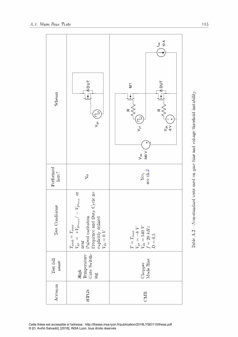
A.1. Main Bias Tests 115
Acronym
Testfull
name
TestConditions
Perform
edhere?
Schema
HTGS
High
Tem
perature
GateSw
itch-
ing
Tamb
=Tmax
Vgs
=+Vgs m
ax/−Vgs m
inor
near
Pulsedexcitation
Frequence
andDutyCycleno
explicitly
den
edVds
=0V
No
DU
T
Vg
s
CMB
Chopp
erModeBias
T=Tmax
Vgs
=−
8V
Vds
=54
0V
f=
20kHz
D=
0.5
Yes,
seech.2
−+54
0V
Vd
d
M1
DU
TI s
w
10A
− +
-8V
Vg
s
R
Vp
1
R
TableA.2
Non-stand
ardtestsused
ongate
bias
andvoltagethresholdinstability.
Cette thèse est accessible à l'adresse : http://theses.insa-lyon.fr/publication/2018LYSEI110/these.pdf © [O. Aviñó Salvadó], [2018], INSA Lyon, tous droits réservés
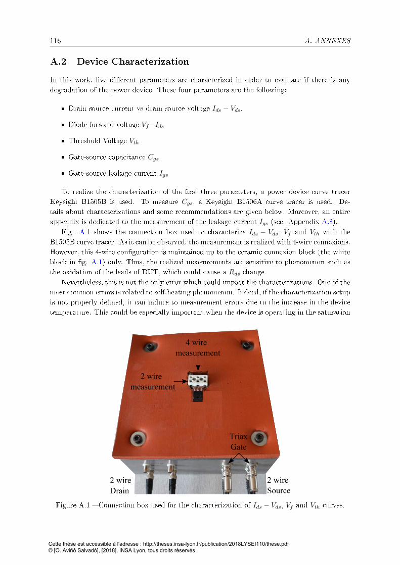
116 A. ANNEXES
A.2 Device Characterization
In this work, ve dierent parameters are characterized in order to evaluate if there is anydegradation of the power device. These four parameters are the following:
Drain-source current vs drain-source voltage Ids − Vds.
Diode forward voltage Vf−Ids
Threshold Voltage Vth
Gate-source capacitance Cgs
Gate-source leakage current Igs
To realize the characterization of the rst three parameters, a power device curve tracerKeysight B1505B is used. To measure Cgs, a Keysight B1506A curve tracer is used. De-tails about characterizations and some recommendations are given below. Moreover, an entireappendix is dedicated to the measurement of the leakage current Igs (see. Appendix A.3).
Fig. A.1 shows the connection box used to characterize Ids − Vds, Vf and Vth with theB1505B curve tracer. As it can be observed, the measurement is realized with 4-wire connexions.However, this 4-wire conguration is maintained up to the ceramic connexion block (the whiteblock in g. A.1) only. Thus, the realized measurements are sensitive to phenomenon such asthe oxidation of the leads of DUT, which could cause a Rds change.
Nevertheless, this is not the only error which could impact the characterizations. One of themost common errors is related to self-heating phenomenon. Indeed, if the characterization setupis not properly dened, it can induce to measurement errors due to the increase in the devicetemperature. This could be especially important when the device is operating in the saturation
2 wireDrain
2 wireSource
TriaxGate
2 wiremeasurement
4 wiremeasurement
Figure A.1 Connection box used for the characterization of Ids − Vds, Vf and Vth curves.
Cette thèse est accessible à l'adresse : http://theses.insa-lyon.fr/publication/2018LYSEI110/these.pdf © [O. Aviñó Salvadó], [2018], INSA Lyon, tous droits réservés
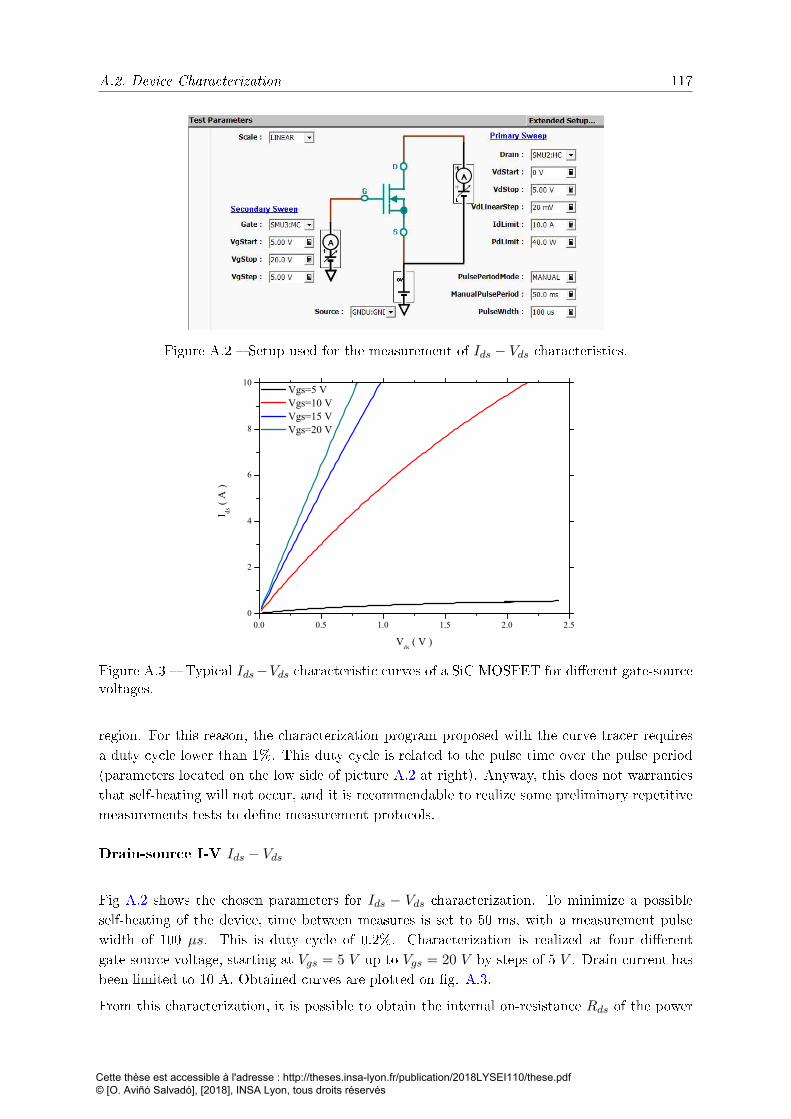
A.2. Device Characterization 117
Figure A.2 Setup used for the measurement of Ids − Vds characteristics.
0.0 0.5 1.0 1.5 2.0 2.50
2
4
6
8
10
I ds(
A )
Vds
( V )
Vgs=5 VVgs=10 VVgs=15 VVgs=20 V
Figure A.3 Typical Ids−Vds characteristic curves of a SiC MOSFET for dierent gate-sourcevoltages.
region. For this reason, the characterization program proposed with the curve tracer requiresa duty cycle lower than 1%. This duty cycle is related to the pulse time over the pulse period(parameters located on the low side of picture A.2 at right). Anyway, this does not warrantiesthat self-heating will not occur, and it is recommendable to realize some preliminary repetitivemeasurements tests to dene measurement protocols.
Drain-source I-V Ids − Vds
Fig A.2 shows the chosen parameters for Ids − Vds characterization. To minimize a possibleself-heating of the device, time between measures is set to 50 ms, with a measurement pulsewidth of 100 µs. This is duty cycle of 0.2%. Characterization is realized at four dierentgate-source voltage, starting at Vgs = 5 V up to Vgs = 20 V by steps of 5 V . Drain current hasbeen limited to 10 A. Obtained curves are plotted on g. A.3.
From this characterization, it is possible to obtain the internal on-resistance Rds of the power
Cette thèse est accessible à l'adresse : http://theses.insa-lyon.fr/publication/2018LYSEI110/these.pdf © [O. Aviñó Salvadó], [2018], INSA Lyon, tous droits réservés
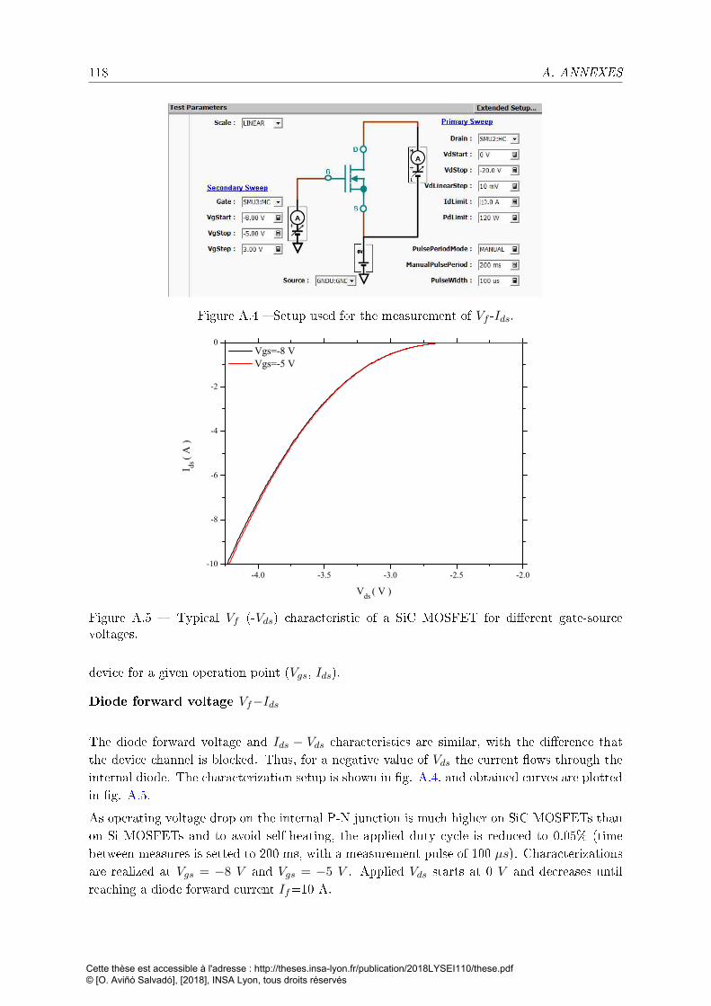
118 A. ANNEXES
Figure A.4 Setup used for the measurement of Vf -Ids.
-4.0 -3.5 -3.0 -2.5 -2.0-10
-8
-6
-4
-2
0
I ds(
A )
Vds ( V )
Vgs=-8 VVgs=-5 V
Figure A.5 Typical Vf (-Vds) characteristic of a SiC MOSFET for dierent gate-sourcevoltages.
device for a given operation point (Vgs, Ids).
Diode forward voltage Vf−Ids
The diode forward voltage and Ids − Vds characteristics are similar, with the dierence thatthe device channel is blocked. Thus, for a negative value of Vds the current ows through theinternal diode. The characterization setup is shown in g. A.4, and obtained curves are plottedin g. A.5.
As operating voltage drop on the internal P-N junction is much higher on SiC MOSFETs thanon Si MOSFETs and to avoid self-heating, the applied duty cycle is reduced to 0.05% (timebetween measures is setted to 200 ms, with a measurement pulse of 100 µs). Characterizationsare realized at Vgs = −8 V and Vgs = −5 V . Applied Vds starts at 0 V and decreases untilreaching a diode forward current If=10 A.
Cette thèse est accessible à l'adresse : http://theses.insa-lyon.fr/publication/2018LYSEI110/these.pdf © [O. Aviñó Salvadó], [2018], INSA Lyon, tous droits réservés
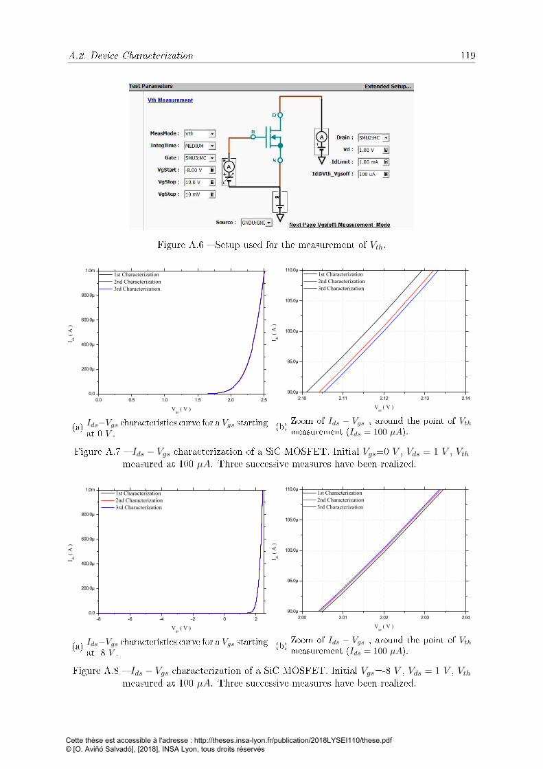
A.2. Device Characterization 119
Figure A.6 Setup used for the measurement of Vth.
0.0 0.5 1.0 1.5 2.0 2.50.0
200.0µ
400.0µ
600.0µ
800.0µ
1.0m
I ds(
A )
Vgs
( V )
1st Characterization2nd Characterization3rd Characterization
(a)Ids−Vgs characteristics curve for a Vgs startingat 0 V .
2.10 2.11 2.12 2.13 2.1490.0µ
95.0µ
100.0µ
105.0µ
110.0µI ds
( A
)
Vgs
( V )
1st Characterization2nd Characterization3rd Characterization
(b)Zoom of Ids − Vgs , around the point of Vthmeasurement (Ids = 100 µA).
Figure A.7 Ids − Vgs characterization of a SiC MOSFET. Initial Vgs=0 V , Vds = 1 V , Vthmeasured at 100 µA. Three successive measures have been realized.
-8 -6 -4 -2 0 20.0
200.0µ
400.0µ
600.0µ
800.0µ
1.0m1st Characterization2nd Characterization3rd Characterization
I ds(
A )
Vgs
( V )
(a)Ids−Vgs characteristics curve for a Vgs startingat -8 V .
2.00 2.01 2.02 2.03 2.0490.0µ
95.0µ
100.0µ
105.0µ
110.0µ
I ds(
A )
Vgs
( V )
1st Characterization2nd Characterization3rd Characterization
(b)Zoom of Ids − Vgs , around the point of Vthmeasurement (Ids = 100 µA).
Figure A.8 Ids − Vgs characterization of a SiC MOSFET. Initial Vgs=-8 V , Vds = 1 V , Vthmeasured at 100 µA. Three successive measures have been realized.
Cette thèse est accessible à l'adresse : http://theses.insa-lyon.fr/publication/2018LYSEI110/these.pdf © [O. Aviñó Salvadó], [2018], INSA Lyon, tous droits réservés
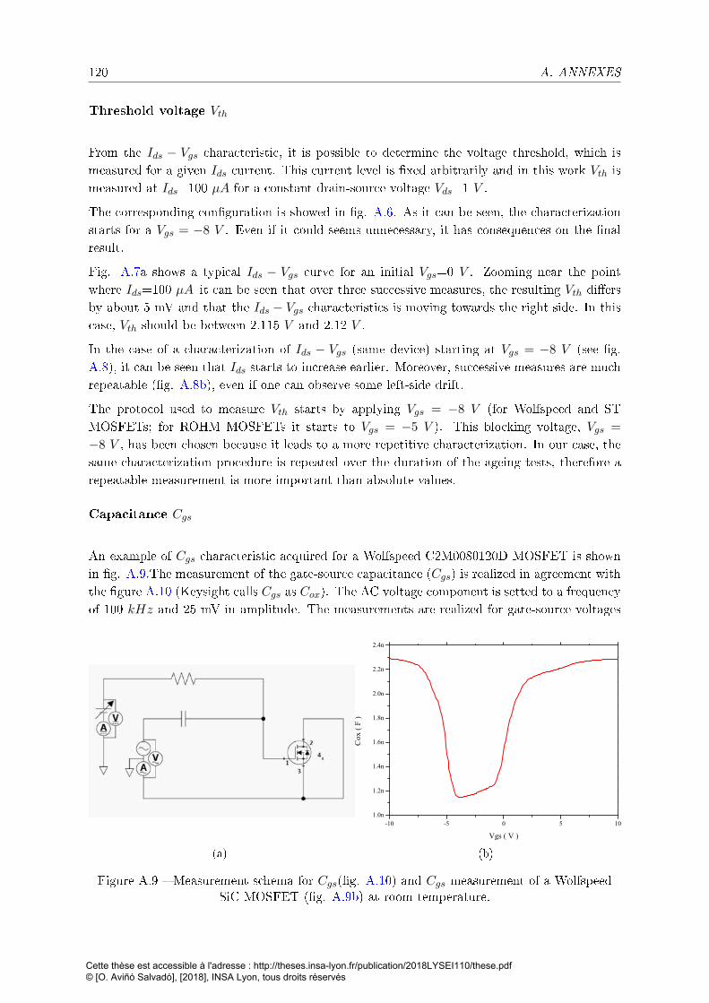
120 A. ANNEXES
Threshold voltage Vth
From the Ids − Vgs characteristic, it is possible to determine the voltage threshold, which ismeasured for a given Ids current. This current level is xed arbitrarily and in this work Vth ismeasured at Ids=100 µA for a constant drain-source voltage Vds=1 V .
The corresponding conguration is showed in g. A.6. As it can be seen, the characterizationstarts for a Vgs = −8 V . Even if it could seems unnecessary, it has consequences on the nalresult.
Fig. A.7a shows a typical Ids − Vgs curve for an initial Vgs=0 V . Zooming near the pointwhere Ids=100 µA it can be seen that over three successive measures, the resulting Vth diersby about 5 mV and that the Ids − Vgs characteristics is moving towards the right side. In thiscase, Vth should be between 2.115 V and 2.12 V .
In the case of a characterization of Ids − Vgs (same device) starting at Vgs = −8 V (see g.A.8), it can be seen that Ids starts to increase earlier. Moreover, successive measures are muchrepeatable (g. A.8b), even if one can observe some left-side drift.
The protocol used to measure Vth starts by applying Vgs = −8 V (for Wolfspeed and STMOSFETs; for ROHM MOSFETs it starts to Vgs = −5 V ). This blocking voltage, Vgs =
−8 V , has been chosen because it leads to a more repetitive characterization. In our case, thesame characterization procedure is repeated over the duration of the ageing tests, therefore arepeatable measurement is more important than absolute values.
Capacitance Cgs
An example of Cgs characteristic acquired for a Wolfspeed C2M0080120D MOSFET is shownin g. A.9.The measurement of the gate-source capacitance (Cgs) is realized in agreement withthe gure A.10 (Keysight calls Cgs as Cox). The AC voltage component is setted to a frequencyof 100 kHz and 25 mV in amplitude. The measurements are realized for gate-source voltages
(a)
-10 -5 0 5 101.0n
1.2n
1.4n
1.6n
1.8n
2.0n
2.2n
2.4n
Cox
( F
)
Vgs ( V )
(b)
Figure A.9 Measurement schema for Cgs(g. A.10) and Cgs measurement of a WolfspeedSiC MOSFET (g. A.9b) at room temperature.
Cette thèse est accessible à l'adresse : http://theses.insa-lyon.fr/publication/2018LYSEI110/these.pdf © [O. Aviñó Salvadó], [2018], INSA Lyon, tous droits réservés
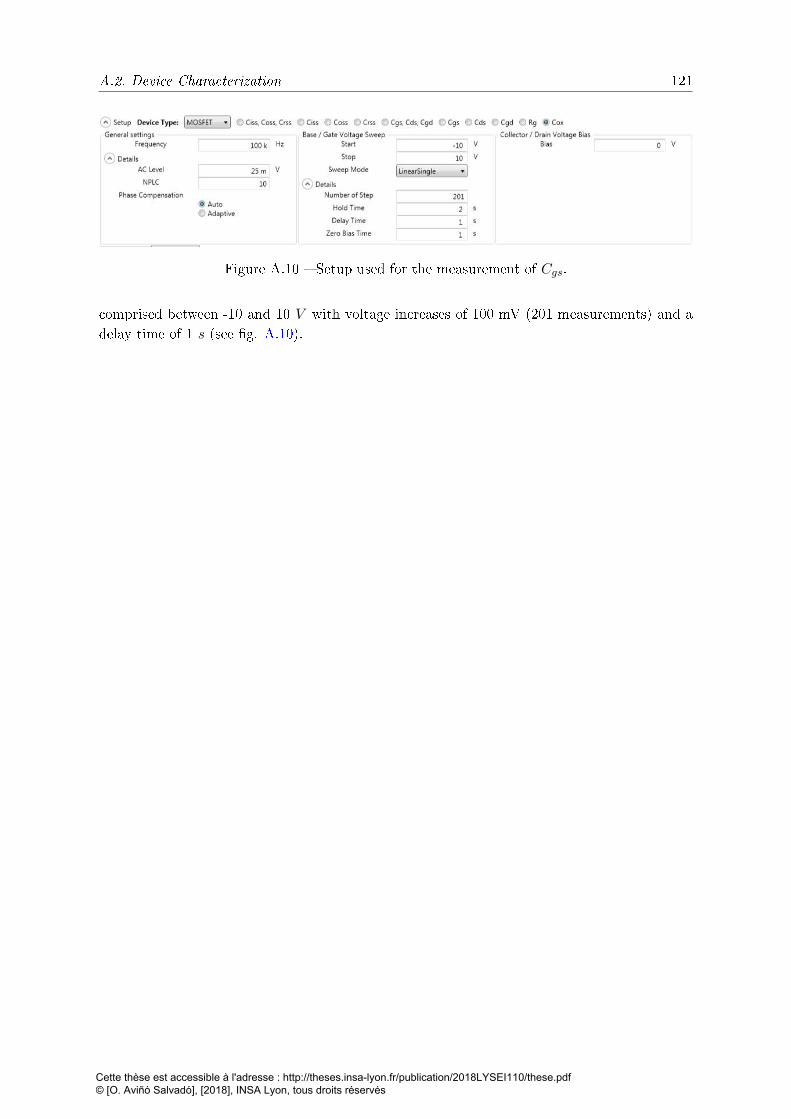
A.2. Device Characterization 121
Figure A.10 Setup used for the measurement of Cgs.
comprised between -10 and 10 V with voltage increases of 100 mV (201 measurements) and adelay time of 1 s (see g. A.10).
Cette thèse est accessible à l'adresse : http://theses.insa-lyon.fr/publication/2018LYSEI110/these.pdf © [O. Aviñó Salvadó], [2018], INSA Lyon, tous droits réservés
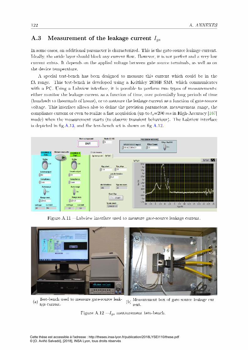
122 A. ANNEXES
A.3 Measurement of the leakage current Igs
In some cases, an additional parameter is characterized. This is the gate-source leakage current.Ideally, the oxide layer should block any current ow. However, it is not perfect and a very lowcurrent exists. It depends on the applied voltage between gate-source terminals, as well as onthe device temperature.
A special test-bench has been designed to measure this current which could be in thefA range. This test-bench is developed using a Keithley 2636B SMU which communicateswith a PC. Using a Labview interface, it is possible to perform two types of measurements:either monitor the leakage current as a function of time, over potentially long periods of time(hundreds to thousands of hours), or to measure the leakage current as a function of gate-sourcevoltage. This interface allows also to dene the precision parameters, measurement range, thecompliance current or even to realize a fast acquisition (up to ts=200ms in High-Accuracy [167]mode) when the measurement starts (to observe transient behaviour). The Labview interfaceis depicted in g.A.13, and the test-bench set is shown on g A.12.
Figure A.11 Labview interface used to measure gate-source leakage current.
(a)Test-bench used to measure gate-source leak-age current.
(b)Measurement box of gate-source leakage cur-rent.
Figure A.12 Igs measurement test-bench.
Cette thèse est accessible à l'adresse : http://theses.insa-lyon.fr/publication/2018LYSEI110/these.pdf © [O. Aviñó Salvadó], [2018], INSA Lyon, tous droits réservés
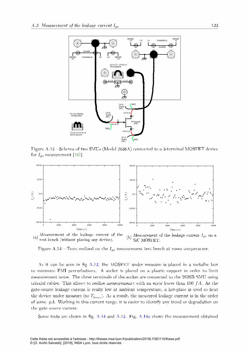
A.3. Measurement of the leakage current Igs 123
Figure A.13 Schema of two SMUs (Model 2636A) connected to a 3-terminal MOSFET devicefor Igs measurement [167].
0 2000 4000 6000 8000 10000-100.0f
-50.0f
0.0
50.0f
100.0f
I gs(
A )
Time ( s )
(a)Measurement of the leakage current of thetest-bench (without placing any device).
0 2000 4000 6000 8000 10000-200.0f
-100.0f
0.0
100.0f
200.0f
I gs(
A )
Time ( s )
(b)Measurement of the leakage current Igs on aSiC MOSFET.
Figure A.14 Tests realized on the Igs measurement test-bench at room temperature.
As it can be seen in g A.12, the MOSFET under measure is placed in a metallic boxto minimize EMI perturbations. A socket is placed on a plastic support in order to limitmeasurement noise. The three terminals of the socket are connected to the 2626B SMU usingtriaxial cables. This allows to realize measurements with an error lower than 100 fA. As thegate-source leakage current is really low at ambient temperature, a hot-plate is used to heatthe device under measure (to Tjmax). As a result, the measured leakage current is in the orderof some pA. Working in this current range, it is easier to identify any trend or degradation onthe gate-source current.
Some tests are shown in g. A.14 and A.15. Fig. A.14a shows the measurement obtained
Cette thèse est accessible à l'adresse : http://theses.insa-lyon.fr/publication/2018LYSEI110/these.pdf © [O. Aviñó Salvadó], [2018], INSA Lyon, tous droits réservés
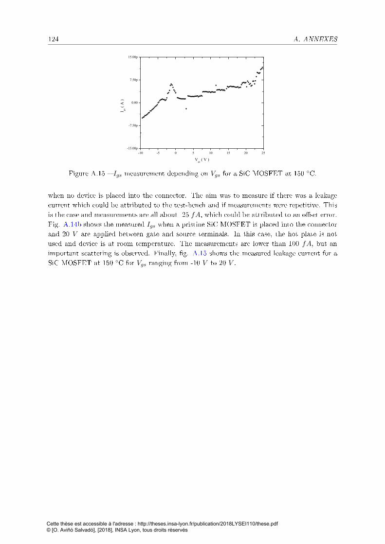
124 A. ANNEXES
-10 -5 0 5 10 15 20 25-15.00p
-7.50p
0.00
7.50p
15.00p
I gs(
A )
Vgs
( V )
Figure A.15 Igs measurement depending on Vgs for a SiC MOSFET at 150 C.
when no device is placed into the connector. The aim was to measure if there was a leakagecurrent which could be attributed to the test-bench and if measurements were repetitive. Thisis the case and measurements are all about -25 fA, which could be attributed to an oset error.Fig. A.14b shows the measured Igs when a pristine SiC MOSFET is placed into the connectorand 20 V are applied between gate and source terminals. In this case, the hot plate is notused and device is at room temperature. The measurements are lower than 100 fA, but animportant scattering is observed. Finally, g. A.15 shows the measured leakage current for aSiC MOSFET at 150 C for Vgs ranging from -10 V to 20 V .
Cette thèse est accessible à l'adresse : http://theses.insa-lyon.fr/publication/2018LYSEI110/these.pdf © [O. Aviñó Salvadó], [2018], INSA Lyon, tous droits réservés
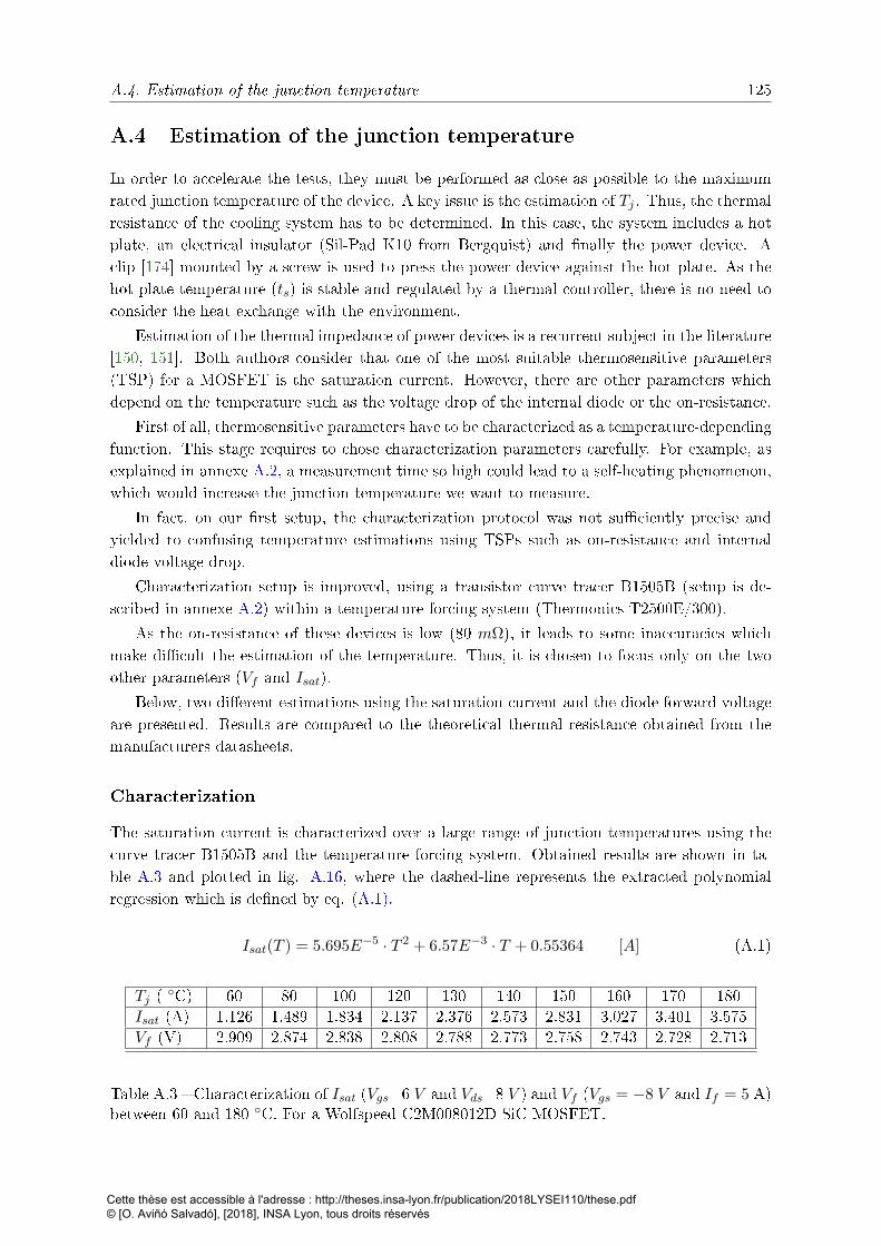
A.4. Estimation of the junction temperature 125
A.4 Estimation of the junction temperature
In order to accelerate the tests, they must be performed as close as possible to the maximumrated junction temperature of the device. A key issue is the estimation of Tj . Thus, the thermalresistance of the cooling system has to be determined. In this case, the system includes a hotplate, an electrical insulator (Sil-Pad K10 from Bergquist) and nally the power device. Aclip [174] mounted by a screw is used to press the power device against the hot plate. As thehot plate temperature (ts) is stable and regulated by a thermal controller, there is no need toconsider the heat exchange with the environment.
Estimation of the thermal impedance of power devices is a recurrent subject in the literature[150, 151]. Both authors consider that one of the most suitable thermosensitive parameters(TSP) for a MOSFET is the saturation current. However, there are other parameters whichdepend on the temperature such as the voltage drop of the internal diode or the on-resistance.
First of all, thermosensitive parameters have to be characterized as a temperature-dependingfunction. This stage requires to chose characterization parameters carefully. For example, asexplained in annexe A.2, a measurement time so high could lead to a self-heating phenomenon,which would increase the junction temperature we want to measure.
In fact, on our rst setup, the characterization protocol was not suciently precise andyielded to confusing temperature estimations using TSPs such as on-resistance and internaldiode voltage drop.
Characterization setup is improved, using a transistor curve tracer B1505B (setup is de-scribed in annexe A.2) within a temperature forcing system (Thermonics T2500E/300).
As the on-resistance of these devices is low (80 mΩ), it leads to some inaccuracies whichmake dicult the estimation of the temperature. Thus, it is chosen to focus only on the twoother parameters (Vf and Isat).
Below, two dierent estimations using the saturation current and the diode forward voltageare presented. Results are compared to the theoretical thermal resistance obtained from themanufacturers datasheets.
Characterization
The saturation current is characterized over a large range of junction temperatures using thecurve tracer B1505B and the temperature forcing system. Obtained results are shown in ta-ble A.3 and plotted in g. A.16, where the dashed-line represents the extracted polynomialregression which is dened by eq. (A.1).
Isat(T ) = 5.695E−5 · T 2 + 6.57E−3 · T + 0.55364 [A] (A.1)
Tj ( C) 60 80 100 120 130 140 150 160 170 180Isat (A) 1.126 1.489 1.834 2.137 2.376 2.573 2.831 3.027 3.401 3.575Vf (V) 2.909 2.874 2.838 2.808 2.788 2.773 2.758 2.743 2.728 2.713
Table A.3 Characterization of Isat (Vgs=6 V and Vds=8 V ) and Vf (Vgs = −8 V and If = 5 A)between 60 and 180 C. For a Wolfspeed C2M008012D SiC MOSFET.
Cette thèse est accessible à l'adresse : http://theses.insa-lyon.fr/publication/2018LYSEI110/these.pdf © [O. Aviñó Salvadó], [2018], INSA Lyon, tous droits réservés
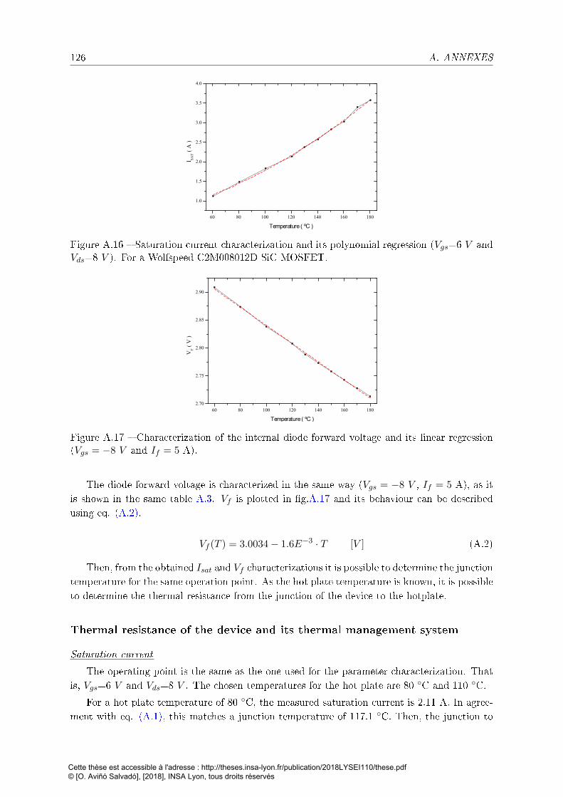
126 A. ANNEXES
60 80 100 120 140 160 180
1.0
1.5
2.0
2.5
3.0
3.5
4.0
I SA
T(
A )
Temperature ( ºC )
Figure A.16 Saturation current characterization and its polynomial regression (Vgs=6 V andVds=8 V ). For a Wolfspeed C2M008012D SiC MOSFET.
60 80 100 120 140 160 1802.70
2.75
2.80
2.85
2.90
VF
( V
)
Temperature ( ºC )
Figure A.17 Characterization of the internal diode forward voltage and its linear regression(Vgs = −8 V and If = 5 A).
The diode forward voltage is characterized in the same way (Vgs = −8 V , If = 5 A), as itis shown in the same table A.3. Vf is plotted in g.A.17 and its behaviour can be describedusing eq. (A.2).
Vf (T ) = 3.0034− 1.6E−3 · T [V ] (A.2)
Then, from the obtained Isat and Vf characterizations it is possible to determine the junctiontemperature for the same operation point. As the hot plate temperature is known, it is possibleto determine the thermal resistance from the junction of the device to the hotplate.
Thermal resistance of the device and its thermal management system
Saturation current
The operating point is the same as the one used for the parameter characterization. Thatis, Vgs=6 V and Vds=8 V . The chosen temperatures for the hot plate are 80 C and 110 C.
For a hot plate temperature of 80 C, the measured saturation current is 2.11 A. In agree-ment with eq. (A.1), this matches a junction temperature of 117.1 C. Then, the junction to
Cette thèse est accessible à l'adresse : http://theses.insa-lyon.fr/publication/2018LYSEI110/these.pdf © [O. Aviñó Salvadó], [2018], INSA Lyon, tous droits réservés
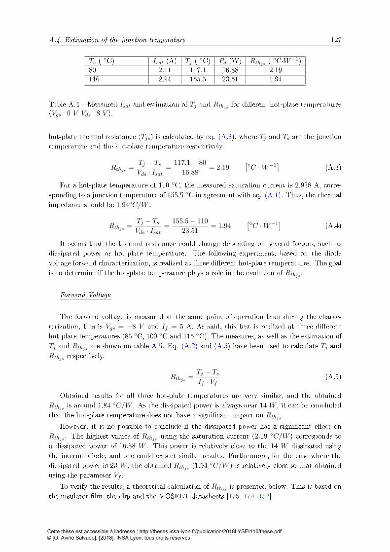
A.4. Estimation of the junction temperature 127
Ts ( C) Isat (A) Tj ( C) Pd (W) Rthjs (C·W−1)
80 2.11 117.1 16.88 2.19110 2.94 155.5 23.51 1.94
Table A.4 Measured Isat and estimation of Tj and Rthjs for dierent hot-plate temperatures(Vgs=6 V Vds=8 V ).
hot-plate thermal resistance (Tjs) is calculated by eq. (A.3), where Tj and Ts are the junctiontemperature and the hot-plate temperature respectively.
Rthjs =Tj − TsVds · Isat
=117.1− 80
16.88= 2.19
[C ·W−1]
(A.3)
For a hot-plate temperature of 110 C, the measured saturation current is 2.938 A, corre-sponding to a junction temperature of 155.5 C in agreement with eq. (A.1). Thus, the thermalimpedance should be 1.94C/W .
Rthjs =Tj − TsVds · Isat
=155.5− 110
23.51= 1.94
[C ·W−1]
(A.4)
It seems that the thermal resistance could change depending on several factors, such asdissipated power or hot-plate temperature. The following experiment, based on the diodevoltage forward characterization, is realized at three dierent hot-plate temperatures. The goalis to determine if the hot-plate temperature plays a role in the evolution of Rthjs .
Forward Voltage
The forward voltage is measured at the same point of operation than during the charac-terization, this is Vgs = −8 V and If = 5 A. As said, this test is realized at three dierenthot-plate temperatures (85 C, 100 C and 115 C). The measures, as well as the estimation ofTj and Rthjs are shown on table A.5. Eq. (A.2) and (A.5) have been used to calculate Tj andRthjs respectively.
Rthjs =Tj − TsIf · Vf
(A.5)
Obtained results for all three hot-plate temperatures are very similar, and the obtainedRthjs is around 1.84 C/W . As the dissipated power is always near 14 W , it can be concludedthat the hot-plate temperature does not have a signicant impact on Rthjs .
However, it is no possible to conclude if the dissipated power has a signicant eect onRthjs . The highest values of Rthjs using the saturation current (2.19 C/W ) corresponds toa dissipated power of 16.88 W . This power is relatively close to the 14 W dissipated usingthe internal diode, and one could expect similar results. Furthermore, for the case where thedissipated power is 23 W , the obtained Rthjs (1.94
C/W ) is relatively close to that obtainedusing the parameter Vf .
To verify the results, a theoretical calculation of Rthjs is presented below. This is based onthe insulator lm, the clip and the MOSFET datasheets [175, 174, 152].
Cette thèse est accessible à l'adresse : http://theses.insa-lyon.fr/publication/2018LYSEI110/these.pdf © [O. Aviñó Salvadó], [2018], INSA Lyon, tous droits réservés
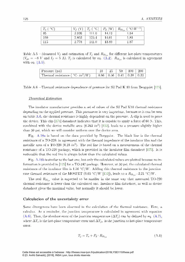
128 A. ANNEXES
Ts ( C) Vf (V) Tj ( C) Pd (W) Rthjs (C·W−1)
85 2.826 111.0 14.13 1.84100 2.803 125.4 14.01 1.81115 2.778 141.0 13.89 1.87
Table A.5 Measured Vf and estimation of Tj and Rthjs for dierent hot-plate temperatures(Vgs = −8 V and If = 5 A). Tj is calculated by eq. (A.2). Rthjs is calculated in agreementwith eq. (A.5).
Pressure (psi) 10 25 50 100 200Thermal resistance ( C· in2/W ) 0.86 0.56 0.41 0.38 0.33
Table A.6 Thermal resistance dependence of pressure for Sil-Pad K-10 from Bergquist [175].
Theoretical Estimation
The insulator manufacturer provides a set of values of the Sil-Pad K10 thermal resistancedepending on the applied pressure. This parameter is very important, because as it can be seenon table A.6, the thermal resistance is highly dependent on the pressure. A clip is used to pressthe device. This clip [174] datasheet indicates that it is capable to apply a force of 60 N. This,combined with the device metallic area (0.263 in2) [152], leads to a pressure slightly higherthan 50 psi, which we will consider uniform over the device area.
Fig. A.18a is based on the data provided by Bergquist. The black line is the thermalresistance of a TO-220, in agreement with the thermal impedance of the insulator lm and themetallic area of a TO-220 (0.18 in2). The red line is based on a measurement of the thermalresistance of a TO-220 package, which is provided in the insulator lm datasheet [175]. It isnoticeable that the red line is always below than the calculated values.
Fig. A.18b is similar to the last one, but only the calculated values are plotted because no in-formation is provided in [175] for a TO-247 package. However, at 50 psi, the calculated thermalresistance of the insulator lm is 1.56 C/W . Adding this thermal resistance to the junction-case thermal resistance of the MOSFET (0.65 C/W [152]), leads to a Rthjs=2.21
C/W .
The real Rthjs value is expected to be smaller in the same way that measured TO-220thermal resistance is lower than the calculated one. Insulator lm datasheet, as well as devicedatasheet gives the maximal value, but normally it should be lower.
Calculation of the uncertainty error
Some divergences have been observed in the calculation of the thermal resistance. Here, acalculus. As a reminder, the junction temperature is calculated in agreement with equation(A.6). Thus, the absolute error of the junction temperature (∆Tj) can by dened by eq. (A.7),where ∆Ts is the hot-plate temperature error and ∆Tjs is the junction to hot-plate temperatureerror.
Tj = Ts + Pd ·Rthjs (A.6)
Cette thèse est accessible à l'adresse : http://theses.insa-lyon.fr/publication/2018LYSEI110/these.pdf © [O. Aviñó Salvadó], [2018], INSA Lyon, tous droits réservés
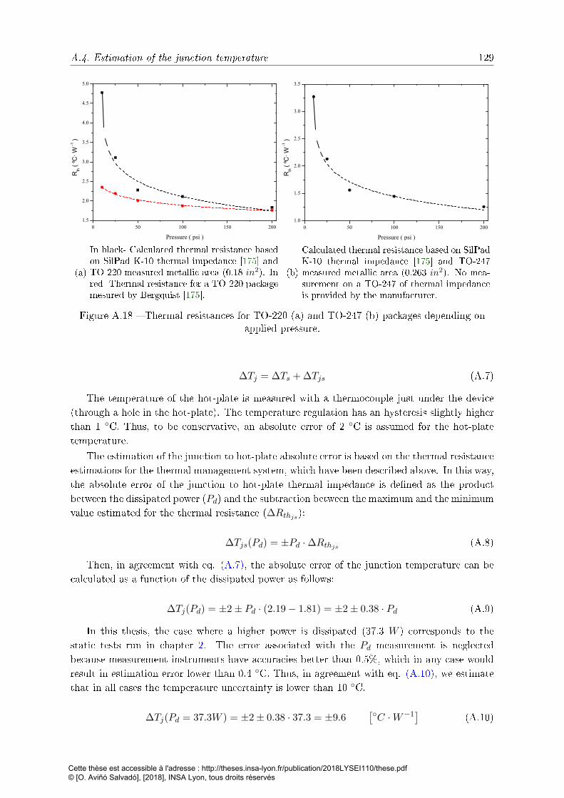
A.4. Estimation of the junction temperature 129
0 50 100 150 2001.5
2.0
2.5
3.0
3.5
4.0
4.5
5.0
Rth
( ºC
· W
-1)
Pressure ( psi )
(a)
In black- Calculated thermal resistance basedon SilPad K-10 thermal impedance [175] andTO-220 measured metallic area (0.18 in2). Inred- Thermal resistance for a TO-220 packagemesured by Bergquist [175].
0 50 100 150 2001.0
1.5
2.0
2.5
3.0
3.5
Rth
( ºC
· W
-1)
Pressure ( psi )
(b)
Calculated thermal resistance based on SilPadK-10 thermal impedance [175] and TO-247measured metallic area (0.263 in2). No mea-surement on a TO-247 of thermal impedanceis provided by the manufacturer.
Figure A.18 Thermal resistances for TO-220 (a) and TO-247 (b) packages depending onapplied pressure.
∆Tj = ∆Ts + ∆Tjs (A.7)
The temperature of the hot-plate is measured with a thermocouple just under the device(through a hole in the hot-plate). The temperature regulation has an hysteresis slightly higherthan 1 C. Thus, to be conservative, an absolute error of 2 C is assumed for the hot-platetemperature.
The estimation of the junction to hot-plate absolute error is based on the thermal resistanceestimations for the thermal management system, which have been described above. In this way,the absolute error of the junction to hot-plate thermal impedance is dened as the productbetween the dissipated power (Pd) and the subtraction between the maximum and the minimumvalue estimated for the thermal resistance (∆Rthjs):
∆Tjs(Pd) = ±Pd ·∆Rthjs (A.8)
Then, in agreement with eq. (A.7), the absolute error of the junction temperature can becalculated as a function of the dissipated power as follows:
∆Tj(Pd) = ±2± Pd · (2.19− 1.81) = ±2± 0.38 · Pd (A.9)
In this thesis, the case where a higher power is dissipated (37.3 W ) corresponds to thestatic tests run in chapter 2. The error associated with the Pd measurement is neglectedbecause measurement instruments have accuracies better than 0.5%, which in any case wouldresult in estimation error lower than 0.4 C. Thus, in agreement with eq. (A.10), we estimatethat in all cases the temperature uncertainty is lower than 10 C.
∆Tj(Pd = 37.3W ) = ±2± 0.38 · 37.3 = ±9.6[C ·W−1
](A.10)
Cette thèse est accessible à l'adresse : http://theses.insa-lyon.fr/publication/2018LYSEI110/these.pdf © [O. Aviñó Salvadó], [2018], INSA Lyon, tous droits réservés
130 A. ANNEXES
Conclusions
Theoretical and experimental calculations of Rthjs have been presented in this annexe. Exper-imental values of Rthjs range between 1.81 and 2.19C/W .
Results using the diode forward voltage as a thermosensitive parameter are more consis-tent than those using the saturation current. Some test have been realized using Rds as athermosensitive parameter, but results were poor and not detailed here.
Test studying the eects of hot-plate temperature and dissipated power on Rthjs havereported that hot-plate temperature does not have a signicant impact. Data about dissipatedpower are not consistent.
The theoretical estimation has found that for a TO-247, the thermal resistance should beRthjs=2.21
C/W . As this calculation is based on the datasheets which includes some safetymargins, it is expected that the actual thermal resistance will be lower. We estimate that thevalues obtained experimentally using the internal diode as a thermosensitive parameter seemsmore realistic (about 1.84C/W ).
In spite of this, in order to avoid device overheating during our tests, it is preferred to beconservative. Thus, in this thesis the Rthjs value used to estimate the junction temperature isthe highest value obtained experimentally, this is 2.19C/W . In addition, a calculation of theuncertainty error (assuming steady-state model) is realized in this annexe, resulting in an errorof the junction temperature lower than 10 C.
Cette thèse est accessible à l'adresse : http://theses.insa-lyon.fr/publication/2018LYSEI110/these.pdf © [O. Aviñó Salvadó], [2018], INSA Lyon, tous droits réservés
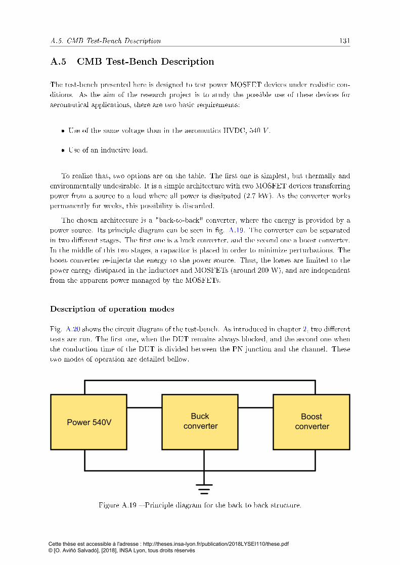
A.5. CMB Test-Bench Description 131
A.5 CMB Test-Bench Description
The test-bench presented here is designed to test power MOSFET devices under realistic con-ditions. As the aim of the research project is to study the possible use of these devices foraeronautical applications, there are two basic requirements:
Use of the same voltage than in the aeronautics HVDC, 540 V .
Use of an inductive load.
To realize that, two options are on the table. The rst one is simplest, but thermally andenvironmentally undesirable. It is a simple architecture with two MOSFET devices transferringpower from a source to a load where all power is dissipated (2.7 kW). As the converter workspermanently for weeks, this possibility is discarded.
The chosen architecture is a "back-to-back" converter, where the energy is provided by apower source. Its principle diagram can be seen in g. A.19. The converter can be separatedin two dierent stages. The rst one is a buck converter, and the second one a boost converter.In the middle of this two stages, a capacitor is placed in order to minimize perturbations. Theboost converter re-injects the energy to the power source. Thus, the losses are limited to thepower energy dissipated in the inductors and MOSFETs (around 200 W), and are independentfrom the apparent power managed by the MOSFETs.
Description of operation modes
Fig. A.20 shows the circuit diagram of the test-bench. As introduced in chapter 2, two dierenttests are run. The rst one, when the DUT remains always blocked, and the second one whenthe conduction time of the DUT is divided between the PN junction and the channel. Thesetwo modes of operation are detailed bellow.
Boost converter
Buck converterPower 540V
Figure A.19 Principle diagram for the back to back structure.
Cette thèse est accessible à l'adresse : http://theses.insa-lyon.fr/publication/2018LYSEI110/these.pdf © [O. Aviñó Salvadó], [2018], INSA Lyon, tous droits réservés

132 A. ANNEXES
−+
540 V
Vdd
M1
DUT
D1
M2
L1
C
L2
−+-8 V
Vgs
R
Vp1
R
Vp2
R
Figure A.20 Schematic of the back to back test-bench (CMB).
−+
540 V
Vdd
M1ON
C
Isw
10 A
IL=10A
Figure A.21 Equivalent circuit diagram and current path when switch M1 is in the on stateand the DUT remains blocked.
CMB test-bench - Channel always blocked -
Circuit conguration M1 On - DUT O
In this case (see g. A.21), the DUT is in the o state (modelled as an open circuit) and theMOSFET M1 is conducting. Its duty cycle (M1) is 0.5. The voltage source supplies energy tothe inductor and IL increases, remaining always near 10 A due to the high inductance value.This ensures that the inductor energy is enough for when the switch M1 is blocked and thishas to supply the required current to stress the DUT.
Circuit conguration M1 O - DUT O
In this case (see g. A.22), asM1 is blocked (modelled as an open circuit), the inductor suppliesthe energy. The DUT also remains blocked. The current ows through the DUT P-N junction,which becomes forward biased at near 10 A.
Cette thèse est accessible à l'adresse : http://theses.insa-lyon.fr/publication/2018LYSEI110/these.pdf © [O. Aviñó Salvadó], [2018], INSA Lyon, tous droits réservés
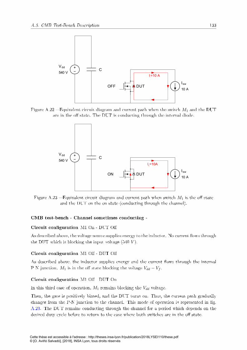
A.5. CMB Test-Bench Description 133
−+
540 V
VddC
DUTOFFIsw
10 A
IL=10 A
Figure A.22 Equivalent circuit diagram and current path when the switch M1 and the DUTare in the o state. The DUT is conducting through the internal diode.
−+
540 V
VddC
DUTONIsw
10 A
IL=10A
Figure A.23 Equivalent circuit diagram and current path when switch M1 is the o stateand the DUT on the on state (conducting through the channel).
CMB test-bench - Channel sometimes conducting -
Circuit conguration M1 On - DUT O
As described above, the voltage source supplies energy to the inductor. No current ows throughthe DUT which is blocking the input voltage (540 V ).
Circuit conguration M1 O - DUT O
As described above, the inductor supplies energy and the current ows through the internalP-N junction. M1 is in the o state blocking the voltage Vdd − Vf .
Circuit conguration M1 O - DUT On
In this third case of operation, M1 remains blocking the Vdd voltage.
Then, the gate is positively biased, and the DUT turns on. Thus, the current path graduallychanges from the P-N junction to the channel. This mode of operation is represented in g.A.23. The DUT remains conducting through the channel for a period which depends on thedesired duty cycle before to return to the case where both switches are in the o state.
Cette thèse est accessible à l'adresse : http://theses.insa-lyon.fr/publication/2018LYSEI110/these.pdf © [O. Aviñó Salvadó], [2018], INSA Lyon, tous droits réservés
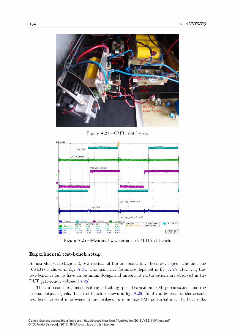
134 A. ANNEXES
High-side Driver
Low-side Driver
DUT DUT VgsLinear regulator
Figure A.24 CMB1 test-bench.
DUT Current
Figure A.25 Measured waveforms on CMB1 test-bench.
Experimental test-bench setup
As introduced in chapter 2, two versions of the test-bench have been developed. The rst one(CMB1) is shown in g. A.24. The main waveforms are depicted in g. A.25. However, thistest-bench is far to have an optimum design and important perturbations are observed in theDUT gate-source voltage (A.25).
Thus, a second test-bench is designed taking special care about EMI perturbations and thedrivers output signals. This test-bench is shown in g. A.26. As it can be seen, in this secondtest-bench several improvements are realized to minimize EMI perturbations; the heat-sinks
Cette thèse est accessible à l'adresse : http://theses.insa-lyon.fr/publication/2018LYSEI110/these.pdf © [O. Aviñó Salvadó], [2018], INSA Lyon, tous droits réservés
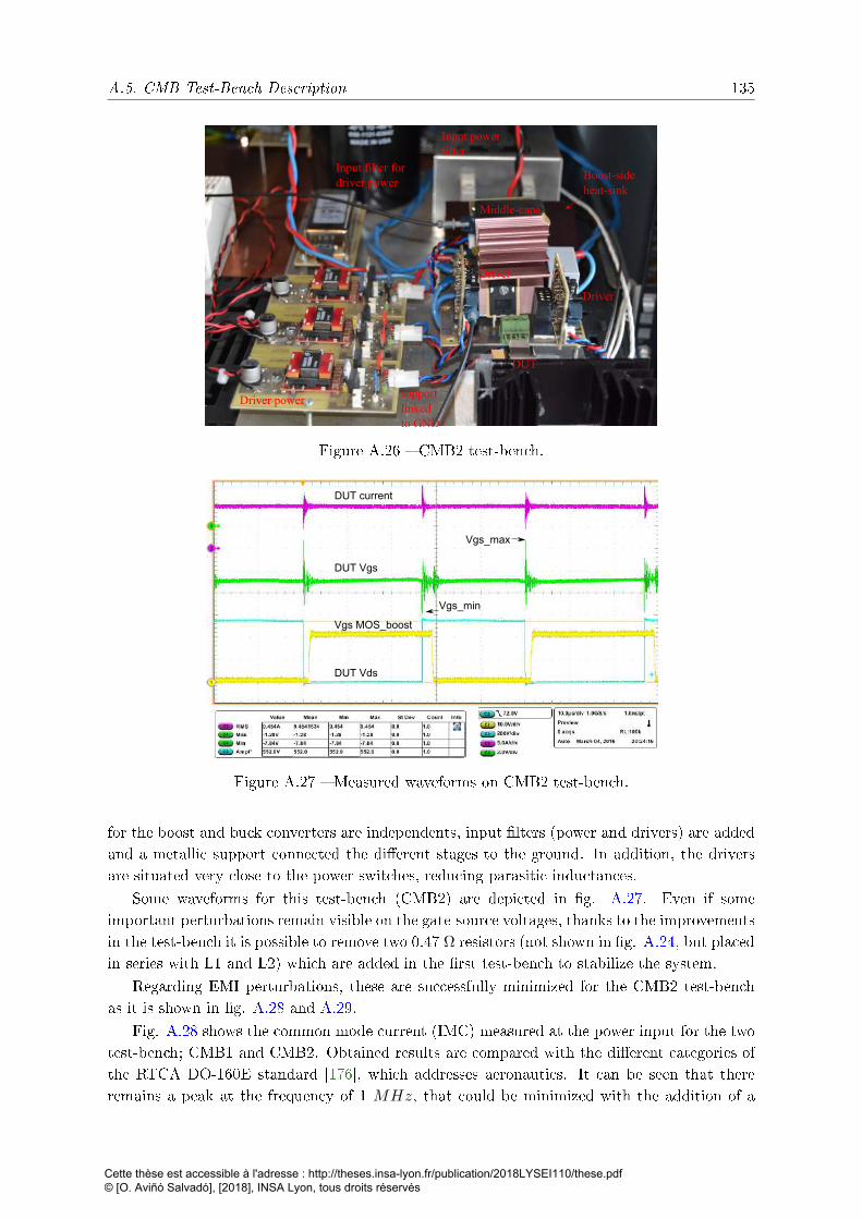
A.5. CMB Test-Bench Description 135
Driver power
Input filter fordriver power
Input powerfilter
Driver
Driver
DUT
Middle-capa
support linked to GND
Boost-sideheat-sink
Figure A.26 CMB2 test-bench.
DUT current
DUT Vgs
Vgs MOS_boost
DUT Vds
Vgs_max
Vgs_min
Figure A.27 Measured waveforms on CMB2 test-bench.
for the boost and buck converters are independents, input lters (power and drivers) are addedand a metallic support connected the dierent stages to the ground. In addition, the driversare situated very close to the power switches, reducing parasitic inductances.
Some waveforms for this test-bench (CMB2) are depicted in g. A.27. Even if someimportant perturbations remain visible on the gate-source voltages, thanks to the improvementsin the test-bench it is possible to remove two 0.47 Ω resistors (not shown in g. A.24, but placedin series with L1 and L2) which are added in the rst test-bench to stabilize the system.
Regarding EMI perturbations, these are successfully minimized for the CMB2 test-benchas it is shown in g. A.28 and A.29.
Fig. A.28 shows the common mode current (IMC) measured at the power input for the twotest-bench; CMB1 and CMB2. Obtained results are compared with the dierent categories ofthe RTCA DO-160E standard [176], which addresses aeronautics. It can be seen that thereremains a peak at the frequency of 1 MHz, that could be minimized with the addition of a
Cette thèse est accessible à l'adresse : http://theses.insa-lyon.fr/publication/2018LYSEI110/these.pdf © [O. Aviñó Salvadó], [2018], INSA Lyon, tous droits réservés
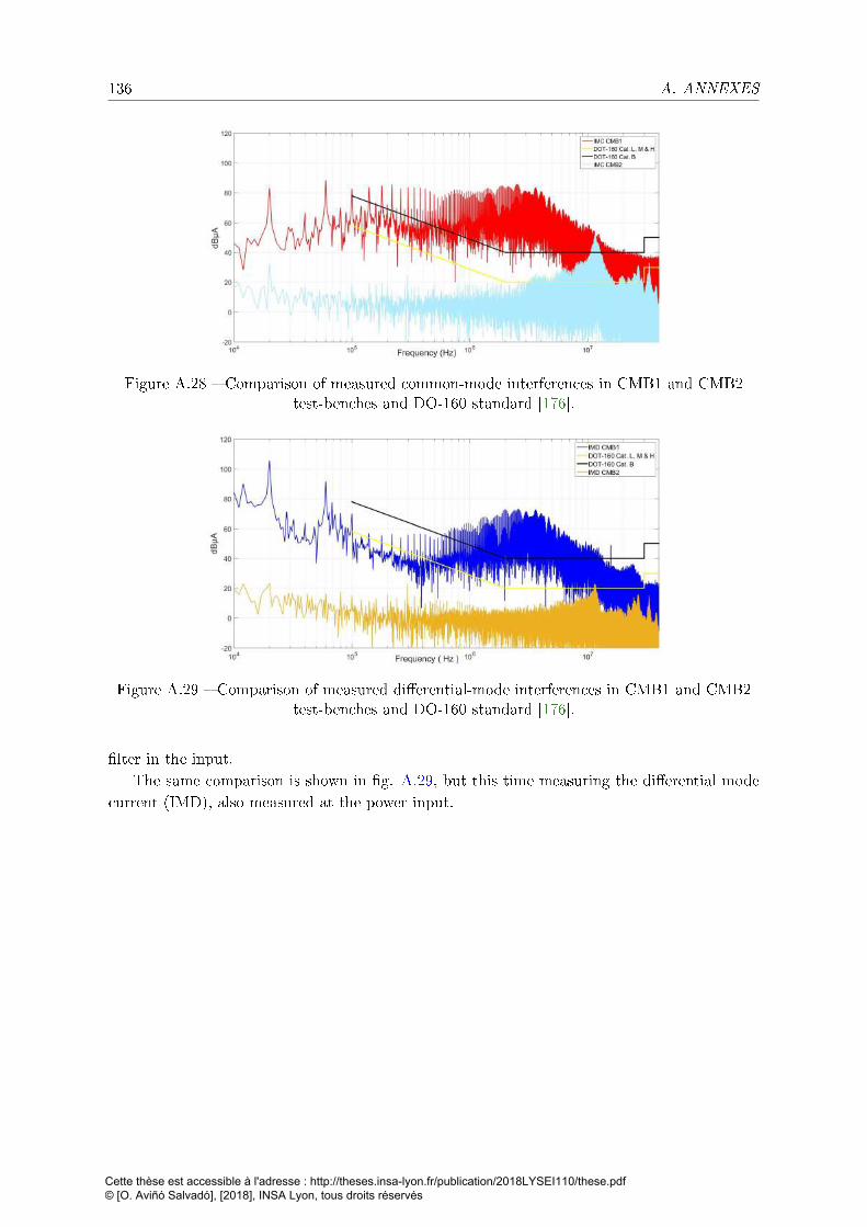
136 A. ANNEXES
Figure A.28 Comparison of measured common-mode interferences in CMB1 and CMB2test-benches and DO-160 standard [176].
Figure A.29 Comparison of measured dierential-mode interferences in CMB1 and CMB2test-benches and DO-160 standard [176].
lter in the input.The same comparison is shown in g. A.29, but this time measuring the dierential mode
current (IMD), also measured at the power input.
Cette thèse est accessible à l'adresse : http://theses.insa-lyon.fr/publication/2018LYSEI110/these.pdf © [O. Aviñó Salvadó], [2018], INSA Lyon, tous droits réservés

A.6. Internal diode robustness data 137
A.6
Internaldioderobustness
data
HTRBTest
DUT1
DUT2
DUT3
DUT4
DUT5
DUT6
DUT7
DUT8
DUT9
DUT10
0h
1.00
1.00
1.00
1.00
1.00
1.00
1.00
1.00
1.00
1.00
15h
1.02
1.00
0.98
0.95
1.01
0.96
1.03
1.06
0.96
1.07
100h
1.16
1.14
1.07
1.09
1.18
1.08
1.15
1.11
1.09
1.15
200h
1.11
1.03
1.04
1.03
1.11
1.04
1.09
1.07
1.00
1.08
300h
1.28
1.19
1.17
1.10
1.21
1.12
1.22
1.16
1.16
1.12
400h
1.23
1.13
1.13
1.07
1.19
1.09
1.11
1.11
1.20
1.22
TableA.7
Normalized
Rdsevolutionover
stress
timeforHTRBtestson
Wolfspeeddevices(C
2M008012D),lot1(R
ef.W14514,
year
2014).
DUT1
DUT2
DUT3
DUT4
DUT5
DUT6
DUT7
DUT8
DUT9
DUT10
0h
1.00
1.00
1.00
1.00
1.00
1.00
1.00
1.00
1.00
1.00
15h
1.01
0.97
1.00
0.98
1.01
0.98
1.01
1.02
0.99
1.02
100h
1.03
1.03
1.02
1.01
1.04
1.00
1.03
1.02
1.01
1.03
200h
1.02
1.00
1.00
0.99
1.02
0.99
1.019
1.02
0.99
1.01
300h
1.05
1.04
1.04
1.00
1.04
1.02
1.04
1.03
1.02
1.02
400h
1.04
1.02
1.03
0.99
1.04
1.00
1.01
1.02
1.02
1.03
TableA.8
Normalized
Vfevolutionover
stress
timeforHTRBtestson
Wolfspeeddevices(C
2M008012D),lot1(R
ef.W14514,
year
2014).
Cette thèse est accessible à l'adresse : http://theses.insa-lyon.fr/publication/2018LYSEI110/these.pdf © [O. Aviñó Salvadó], [2018], INSA Lyon, tous droits réservés
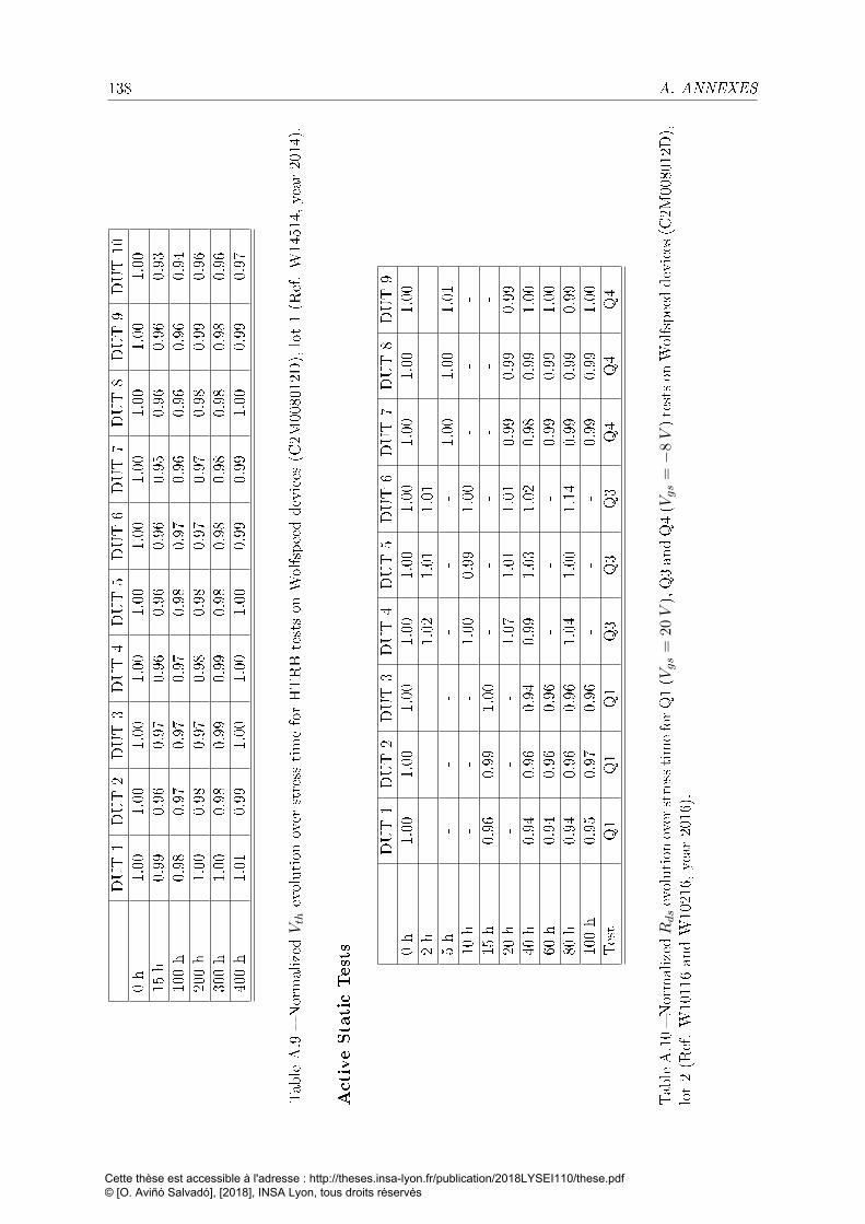
138 A. ANNEXES
DUT1
DUT2
DUT3
DUT4
DUT5
DUT6
DUT7
DUT8
DUT9
DUT10
0h
1.00
1.00
1.00
1.00
1.00
1.00
1.00
1.00
1.00
1.00
15h
0.99
0.96
0.97
0.96
0.96
0.96
0.95
0.96
0.96
0.93
100h
0.98
0.97
0.97
0.97
0.98
0.97
0.96
0.96
0.96
0.94
200h
1.00
0.98
0.97
0.98
0.98
0.97
0.97
0.98
0.99
0.96
300h
1.00
0.98
0.99
0.99
0.98
0.98
0.98
0.98
0.98
0.96
400h
1.01
0.99
1.00
1.00
1.00
0.99
0.99
1.00
0.99
0.97
TableA.9
Normalized
Vth
evolutionover
stress
timeforHTRBtestson
Wolfspeeddevices(C
2M008012D),lot1(R
ef.W14514,
year
2014).
ActiveStaticTests
DUT1
DUT2
DUT3
DUT4
DUT5
DUT6
DUT7
DUT8
DUT9
0h
1.00
1.00
1.00
1.00
1.00
1.00
1.00
1.00
1.00
2h
--
-1.02
1.01
1.01
--
-5h
--
--
--
1.00
1.00
1.01
10h
--
-1.00
0.99
1.00
--
-15
h0.96
0.99
1.00
--
--
--
20h
--
-1.07
1.01
1.01
0.99
0.99
0.99
40h
0.94
0.96
0.94
0.99
1.03
1.02
0.98
0.99
1.00
60h
0.94
0.96
0.96
--
-0.99
0.99
1.00
80h
0.94
0.96
0.96
1.04
1.00
1.14
0.99
0.99
0.99
100h
0.95
0.97
0.96
--
-0.99
0.99
1.00
Test
Q1
Q1
Q1
Q3
Q3
Q3
Q4
Q4
Q4
TableA.10NormalizedRdsevolutionoverstresstimeforQ1(Vgs
=20V),Q3andQ4(Vgs
=−
8V)testson
Wolfspeeddevices(C
2M008012D),
lot2(R
ef.W10116andW10216,
year
2016).
Cette thèse est accessible à l'adresse : http://theses.insa-lyon.fr/publication/2018LYSEI110/these.pdf © [O. Aviñó Salvadó], [2018], INSA Lyon, tous droits réservés
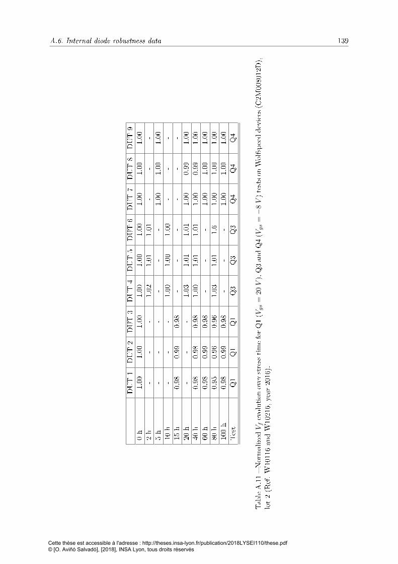
A.6. Internal diode robustness data 139
DUT1
DUT2
DUT3
DUT4
DUT5
DUT6
DUT7
DUT8
DUT9
0h
1.00
1.00
1.00
1.00
1.00
1.00
1.00
1.00
1.00
2h
--
-1.02
1.01
1.01
--
-5h
--
--
--
1.00
1.00
1.00
10h
--
-1.00
1.00
1.00
--
-15
h0.98
0.99
0.98
--
--
--
20h
--
-1.03
1.01
1.01
1.00
0.99
1.00
40h
0.98
0.98
0.98
1.00
1.01
1.01
1.00
0.99
1.00
60h
0.98
0.99
0.98
--
-1.00
1.00
1.00
80h
0.95
0.96
0.96
1.03
1.01
1.6
1.00
1.00
1.00
100h
0.98
0.99
0.98
--
-1.00
1.00
1.00
Test
Q1
Q1
Q1
Q3
Q3
Q3
Q4
Q4
Q4
TableA.11NormalizedVfevolutionoverstresstimeforQ1(Vgs
=20V),Q3andQ4(Vgs
=−
8V)testson
Wolfspeeddevices(C
2M008012D),
lot2(R
ef.W10116andW10216,
year
2016).
Cette thèse est accessible à l'adresse : http://theses.insa-lyon.fr/publication/2018LYSEI110/these.pdf © [O. Aviñó Salvadó], [2018], INSA Lyon, tous droits réservés
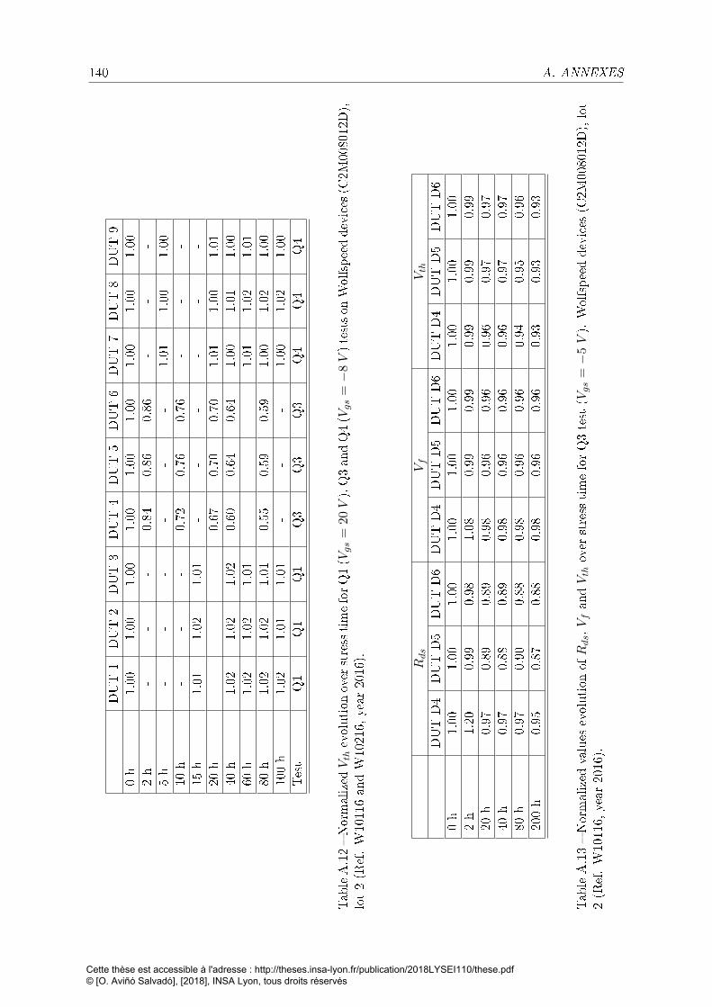
140 A. ANNEXES
DUT1
DUT2
DUT3
DUT4
DUT5
DUT6
DUT7
DUT8
DUT9
0h
1.00
1.00
1.00
1.00
1.00
1.00
1.00
1.00
1.00
2h
--
-0.84
0.86
0.86
--
-5h
--
--
--
1.01
1.00
1.00
10h
--
-0.72
0.76
0.76
--
-15
h1.01
1.02
1.01
--
--
--
20h
--
-0.67
0.70
0.70
1.01
1.00
1.01
40h
1.02
1.02
1.02
0.60
0.64
0.64
1.00
1.01
1.00
60h
1.02
1.02
1.01
--
-1.01
1.02
1.01
80h
1.02
1.02
1.01
0.55
0.59
0.59
1.00
1.02
1.00
100h
1.02
1.01
1.01
--
-1.00
1.02
1.00
Test
Q1
Q1
Q1
Q3
Q3
Q3
Q4
Q4
Q4
TableA.12NormalizedVthevolutionoverstresstimeforQ1(Vgs
=20V),Q3andQ4(Vgs
=−
8V)testson
Wolfspeeddevices(C
2M008012D),
lot2(R
ef.W10116andW10216,
year
2016).
Rds
Vf
Vth
DUTD4
DUTD5
DUTD6
DUTD4
DUTD5
DUTD6
DUTD4
DUTD5
DUTD6
0h
1.00
1.00
1.00
1.00
1.00
1.00
1.00
1.00
1.00
2h
1.20
0.99
0.98
1.08
0.99
0.99
0.99
0.99
0.99
20h
0.97
0.89
0.89
0.98
0.96
0.96
0.96
0.97
0.97
40h
0.97
0.88
0.89
0.98
0.96
0.96
0.96
0.97
0.97
80h
0.97
0.90
0.88
0.98
0.96
0.96
0.94
0.95
0.96
200h
0.95
0.87
0.88
0.98
0.96
0.96
0.93
0.93
0.93
TableA.13Normalized
values
evolutionofRds,VfandVthover
stresstimeforQ3test(Vgs
=−
5V).Wolfspeeddevices(C
2M008012D),lot
2(R
ef.W10116,
year
2016).
Cette thèse est accessible à l'adresse : http://theses.insa-lyon.fr/publication/2018LYSEI110/these.pdf © [O. Aviñó Salvadó], [2018], INSA Lyon, tous droits réservés

A.6. Internal diode robustness data 141
CMBTest-Channelalwaysblocked-
DUTC4
DUTC5
DUTC6
DUTC7
DUTC8
DUTC9
DUTC10
DUTC11
DUTC12
DUTC13
0h
1.00
1.00
1.00
1.00
1.00
1.00
1.00
1.00
1.00
1.00
10h
0.6
1.06
1.20
1.12
0.85
0.82
0.92
0.94
0.98
0.98
20h
-1.10
1.22
1.16
0.84
0.82
0.90
0.95
0.97
0.98
40h
-1.15
1.11
1.05
0.83
0.83
0.91
0.94
0.97
0.96
60h
-1.22
1.12
0.99
0.89
0.84
0.90
0.93
0.98
0.96
80h
-1.08
1.08
1.00
0.88
1.01
0.94
0.95
0.98
0.98
100h
-1.01
0.89
0.91
1.07
1.00
0.95
0.94
0.99
1.01
TableA.14Normalized
Rdsevolutionover
stresstimeforCMB1testson
Wolfspeeddevices(C
2M008012D),lot1(R
ef.W14514,year
2014).
DUTC4
DUTC5
DUTC6
DUTC7
DUTC8
DUTC9
DUTC10
DUTC11
DUTC12
DUTC13
0h
1.00
1.00
1.00
1.00
1.00
1.00
1.00
1.00
1.00
1.00
10h
0.86
1.03
1.05
1.02
0.96
0.99
1.00
1.02
1.01
1.00
20h
-1.02
1.04
1.03
0.97
0.99
1.00
1.01
1.01
1.01
40h
-1.03
1.03
1.03
0.96
0.95
1.00
1.02
1.01
1.01
60h
-1.06
1.03
1.00
0.98
0.99
1.00
1.02
1.01
1.01
80h
-1.03
1.01
1.00
0.98
1.01
0.99
1.01
1.01
1.01
100h
-1.00
0.98
0.97
1.02
1.01
0.98
1.02
1.01
1.00
TableA.15Normalized
Vfevolutionover
stress
timeforCMB1testson
Wolfspeeddevices(C
2M008012D),lot1(R
ef.W14514,
year
2014).
Cette thèse est accessible à l'adresse : http://theses.insa-lyon.fr/publication/2018LYSEI110/these.pdf © [O. Aviñó Salvadó], [2018], INSA Lyon, tous droits réservés

142 A. ANNEXES
DUTC4
DUTC5
DUTC6
DUTC7
DUTC8
DUTC9
DUTC10
DUTC11
DUTC12
DUTC13
0h
1.00
1.00
1.00
1.00
1.00
1.00
1.00
1.00
1.00
1.00
10h
0.25
0.91
0.89
0.89
0.90
0.90
0.88
0.90
0.90
0.88
20h
-0.86
0.87
0.88
0.88
0.88
0.86
0.87
0.89
0.86
40h
-0.84
0.84
0.86
0.86
0.84
0.82
0.84
0.87
0.84
60h
-0.84
0.82
0.85
0.85
0.83
0.80
0.86
0.86
0.82
80h
-0.82
0.80
0.83
0.85
0.79
0.77
0.84
0.84
0.83
100h
-0.82
0.82
0.81
0.82
0.79
0.75
0.84
0.82
0.80
TableA.16Normalized
Vthevolutionover
stress
timeforCMB1testson
Wolfspeeddevices(C
2M008012D),lot1(R
ef.W14514,year
2014).
DUTR1
DUTR2
DUTR3
DUTST
1DUTST
2DUTST
30h
1.00
1.00
1.00
1.00
1.00
1.00
20h
0.86
0.94
0.88
1.03
1.02
1.02
40h
0.86
0.94
0.88
1.03
1.02
1.02
60h
0.88
0.94
0.87
1.03
1.02
1.03
80h
0.91
0.93
0.87
0.99
1.03
1.03
100h
0.87
0.93
0.88
1.02
1.02
1.02
Manufacturer
ROHM
ROHM
ROHM
STST
ST
TableA.17Normalized
Rdsevolutionover
stress
timeforCMB1testson
ROHM
SCT2080KE(R
ef.15-04,
year
2015)andST
SCT30N120
(Ref.CHN-G
K-552,year
2015)devices.
Cette thèse est accessible à l'adresse : http://theses.insa-lyon.fr/publication/2018LYSEI110/these.pdf © [O. Aviñó Salvadó], [2018], INSA Lyon, tous droits réservés

A.6. Internal diode robustness data 143
DUTR1
DUTR2
DUTR3
DUTST
1DUTST
2DUTST
30h
1.00
1.00
1.00
1.00
1.00
1.00
20h
0.98
0.99
0.98
1.00
1.00
1.00
40h
0.98
0.99
0.98
1.00
1.00
1.00
60h
0.98
0.99
0.98
1.00
1.00
1.00
80h
0.98
0.99
0.98
1.00
1.00
1.00
100h
0.99
0.99
0.98
1.00
1.00
1.00
Manufacturer
ROHM
ROHM
ROHM
STST
ST
TableA.18Normalized
Vfevolutionover
stress
timeforCMB1testson
ROHM
SCT2080KE(R
ef.15-04,
year
2015)andST
SCT30N120
(Ref.CHN-G
K-552,year
2015)devices.
DUTR1
DUTR2
DUTR3
DUTST
1DUTST
2DUTST
30h
1.00
1.00
1.00
1.00
1.00
1.00
20h
1.00
0.98
0.99
0.97
0.96
0.97
40h
1.01
0.98
0.98
0.96
0.96
0.96
60h
0.99
0.98
1.00
0.96
0.95
0.96
80h
0.97
1.00
1.00
0.96
0.96
0.96
100h
1.01
0.99
1.03
0.96
0.95
0.95
Manufacturer
ROHM
ROHM
ROHM
STST
ST
TableA.19Normalized
Rdsevolutionover
stress
timeforCMB1testson
ROHM
SCT2080KE(R
ef.15-04,
year
2015)andST
SCT30N120
(Ref.CHN-G
K-552,year
2015)devices.
Cette thèse est accessible à l'adresse : http://theses.insa-lyon.fr/publication/2018LYSEI110/these.pdf © [O. Aviñó Salvadó], [2018], INSA Lyon, tous droits réservés
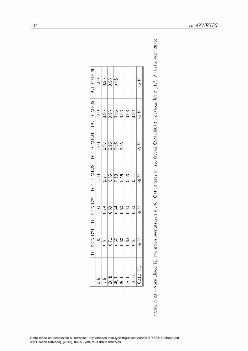
144 A. ANNEXES
DUTCMB21
DUTCMB22
DUTCMB23
DUTCMB24
DUTCMB25
DUTCMB26
0h
1.00
1.00
1.00
1.00
1.00
1.00
5h
0.81
0.79
0.77
0.97
0.95
0.96
20h
0.71
0.69
0.65
0.96
0.95
0.95
40h
0.65
0.64
0.59
0.96
0.93
0.95
60h
0.63
0.63
0.56
0.95
0.93
-80
h0.62
0.60
0.53
-0.93
-100h
0.61
0.60
0.51
-0.93
-CMBVgs
-8V
-8V
-8V
-5V
-5V
-5V
TableA.20Normalized
Vth
evolutionover
stress
timeforCMB2testson
WolfspeedC2M
008012Ddevices,lot2(R
ef.W10216,
year
2016).
Cette thèse est accessible à l'adresse : http://theses.insa-lyon.fr/publication/2018LYSEI110/these.pdf © [O. Aviñó Salvadó], [2018], INSA Lyon, tous droits réservés

A.6. Internal diode robustness data 145
CMBTest-Channelsometimesconducting-
Rds
Vf
Vth
DUT005
DUT015
DUT085
DUT005
DUT015
DUT085
DUT005
DUT015
DUT085
0h
1.00
1.00
1.00
1.00
1.00
1.00
1.00
1.00
1.00
10h
0.99
0.99
1.00
1.00
1.00
1.01
0.95
0.97
1.03
20h
1.00
1.25
0.99
1.00
1.04
1.01
0.94
0.97
1.04
40h
1.23
1.01
0.99
1.03
1.00
1.01
0.93
0.97
1.06
60h
1.02
1.01
1.01
1.00
1.00
1.00
0.94
0.98
1.06
80h
1.03
1.01
1.01
1.00
1.00
1.01
0.94
0.98
1.07
100h
1.03
1.01
1.03
1.00
1.00
1.01
0.93
0.99
1.09
Dutycycle
0.05
0.15
0.85
0.05
0.15
0.85
0.05
0.15
0.85
TableA.21Normalized
values
evolutionofRds,VfandVthover
stresstimeforCMB1testsin
thecase
where
thechannelisused.Wolfspeed
devices(C
2M008012D),lot1(R
ef.W14514,
year
2014).
Cette thèse est accessible à l'adresse : http://theses.insa-lyon.fr/publication/2018LYSEI110/these.pdf © [O. Aviñó Salvadó], [2018], INSA Lyon, tous droits réservés

Cette thèse est accessible à l'adresse : http://theses.insa-lyon.fr/publication/2018LYSEI110/these.pdf © [O. Aviñó Salvadó], [2018], INSA Lyon, tous droits réservés
Bibliography
[1] Joseph Wilson Swan. peters. US Patent 233,445. 1880 (cit. on p. 1).
[2] "IEA". Key World Energy Statistics 2016. Paris: IEA, 2016. doi: http://dx.doi.org/10.1787/key_energ_stat-2016-en (cit. on pp. 1, 2).
[3] Muhammad H Rashid. Power electronics: circuits, devices, and applications. PearsonEducation India, 2009 (cit. on p. 1).
[4] John Bardeen and Walter Hauser Brattain. The transistor, a semi-conductor triode.In: Physical Review 74.2 (1948), p. 230 (cit. on p. 1).
[5] Mary Bellis. Inventors-Electric Cars (1890-1930). In: Inventors. about. com. Retrieved(2010), pp. 1226 (cit. on p. 2).
[6] FA Wyczalek. GM electric vehicle technology. In: INTERNATIONAL SYMPOSIUMON AUTOMOTIVE TECHNOLOGY. 1991 (cit. on p. 2).
[7] Brian Walsh and Peter Moores. Auto Companies On Fuel Cells. In: Fuel Cells (2000)(cit. on p. 3).
[8] Shanta Barley. Hydrogen bus launched on London tourist route. In: The Guardian(2010) (cit. on p. 3).
[9] M. Kanechika, T. Uesugi, and T. Kachi. Advanced SiC and GaN power electronics forautomotive systems. In: 2010 International Electron Devices Meeting. 2010, pp. 13.5.113.5.4. doi: 10.1109/IEDM.2010.5703356 (cit. on p. 3).
[10] George Woodman Hilton and John Fitzgerald Due. The electric interurban railways inAmerica. Stanford University Press, 2000 (cit. on p. 3).
[11] Siemens A.G. 1879 Siemens presents the world's rst electric railway with an externalpower source. url: https://www.siemens.com/history/en/news/electric_railway.htm (cit. on p. 3).
[12] Michael C Duy. Electric Railways: 1880-1990. 31. Iet, 2003 (cit. on p. 3).
[13] Study Electrical.Com. How Electric Locomotives (Electric Trains) Work? 2014. url:http://www.studyelectrical.com/2014/05/how-electric-locomotives-work.html
(cit. on p. 4).
[14] Bilal Ahmad et al. Wide Band Gap Power Semiconductor Devices and their Applica-tions. In: (2015) (cit. on p. 3).
Cette thèse est accessible à l'adresse : http://theses.insa-lyon.fr/publication/2018LYSEI110/these.pdf © [O. Aviñó Salvadó], [2018], INSA Lyon, tous droits réservés
148 BIBLIOGRAPHY
[15] M Piton. Future Railway Traction Drives based on SiC technology. In: Nuremberg:ECPE SiC & GaN User Forum, 2017 (cit. on p. 4).
[16] X Roboam. Réseaux de bord électriques en aéronautique. In: Lille: Journées Elec-trotechnique du club EEA, 2009 (cit. on p. 5).
[17] Pat Wheeler. The More Electric Aircraft: Why Aerospace Needs Power Electronics?In: Barcelona: 13th European Conference on Power Electronics and Aplications, 2009(cit. on pp. 4, 5, 68).
[18] Mike Sinnett. 787 No-Bleed Systems: Saving Fuel and Enhancing Operational Ecien-cies. 2007. url: http://www.boeing.com/commercial/aeromagazine/articles/qtr_4_07/AERO_Q407_article2.pdf (cit. on pp. 4, 5, 68).
[19] Johannes Brombach et al. Optimizing the weight of an aircraft power supply systemthrough a+/-270 VDC main voltage. In: Gen 360 (2012), p. 800 (cit. on p. 5).
[20] Lidia ukasiak and Andrzej Jakubowski. History of semiconductors. In: Journal ofTelecommunications and information technology (2010), pp. 39 (cit. on p. 7).
[21] B. Jayant Baliga. Fundamentals of Power Semiconductor Devices. 1st ed. Springer Pub-lishing Company, Incorporated, 2008. isbn: 0387473130, 9780387473130 (cit. on pp. 7,921, 27, 30, 32, 42, 43).
[22] Cyril Buttay et al. State of the art of high temperature power electronics. In:MaterialsScience and Engineering: B 176.4 (2011), pp. 283288 (cit. on p. 7).
[23] J Berzelius. Undersökning af några mineralier. In: (1824) (cit. on p. 8).
[24] E. G. Acheson. Production of Artical Crystalline Carbonaceous Materials. 1895 (cit. onp. 8).
[25] Michael E Levinshtein, Sergey L Rumyantsev, and Michael S Shur. Properties of Ad-vanced Semiconductor Materials: GaN, AIN, InN, BN, SiC, SiGe. John Wiley & Sons,2001 (cit. on p. 8).
[26] J.A. Lely. Sublimation process for manufacturing Silicon Carbide crystals. In: US Pat.2,854,364 (1958) (cit. on p. 8).
[27] L.J. Kroko and C.H. Chi. Fused junctions in silicon carbide. US Patent 2,937,323. 1960(cit. on p. 8).
[28] L.J. Kroko. Silicon carbide rectier. US Patent 2,937,324. 1960 (cit. on p. 8).
[29] R.N. Hall. Silicon carbide semiconductor devices and method of preparation thereof. USPatent 2,918,396. 1959 (cit. on p. 8).
[30] H. Albert, H.J. Van Daal, and K.W. Franciscus. Silicon carbide semiconductor device.US Patent 3,121,829. 1964 (cit. on p. 8).
[31] Hugh O. Pierson. Handbook of Refractory Carbides and Nitrides. In: Handb. Refract.Carbides Nitrides (1996), pp. 816. issn: 00225088. doi: 10.1016/B978-081551392-6.50003-9. arXiv: arXiv:1011.1669v3 (cit. on p. 8).
[32] Jacques Botsoa. Synthèse de nanostructures de carbure de silicium et étude de leurspropriétés optiques. In: Lyon: INSA de Lyon (2008) (cit. on p. 8).
Cette thèse est accessible à l'adresse : http://theses.insa-lyon.fr/publication/2018LYSEI110/these.pdf © [O. Aviñó Salvadó], [2018], INSA Lyon, tous droits réservés
BIBLIOGRAPHY 149
[33] Andreas Fissel. Articially layered heteropolytypic structures based on SiC polytypes:molecular beam epitaxy, characterization and properties. In: Physics reports 379.3(2003), pp. 149255 (cit. on p. 8).
[34] Lewis Stephen Ramsdell. Studies on silicon carbide. In: American Mineralogist 32.1-2(1947), pp. 6482 (cit. on p. 8).
[35] T Ayalew. SiC Semiconductor Devices Technology, Modeling, and Simulation. 2004. url:http://www.iue.tuwien.ac.at/phd/ayalew/node20.html (cit. on p. 9).
[36] J. W. Palmour et al. 6H-silicon carbide devices and applications. In: Phys. B Phys.Condens. Matter 185.1-4 (1993), pp. 461465. issn: 09214526. doi: 10.1016/0921-4526(93)90278-E (cit. on p. 8).
[37] SI Vlaskina. Silicon carbide LED. In: Semiconductor Physics Quantum Electronics &Optoelectronics (2002) (cit. on p. 8).
[38] Rositza Yakimova et al. Progress in 3C-SiC growth and novel applications. In: Mate-rials Science Forum. Vol. 711. Trans Tech Publ. 2012, pp. 310 (cit. on p. 8).
[39] Bart Van Zeghbroeck. Principles of semiconductor devices. In: Colarado University(2004) (cit. on pp. 13, 43).
[40] Nicolas G Wright et al. Electrothermal simulation of 4H-SiC power devices. In: Mate-rials science forum. Vol. 264. Trans Tech Publ. 1998, pp. 917920 (cit. on p. 14).
[41] AG Chynoweth. Ionization rates for electrons and holes in silicon. In: physical review109.5 (1958), p. 1537 (cit. on p. 15).
[42] AG Chynoweth. Uniform Silicon p-n Junctions. II. Ionization Rates for Electrons. In:Journal of Applied Physics 31.7 (1960), pp. 11611165 (cit. on p. 15).
[43] Siméon Denis Poisson. Remarques sur une équation qui se présente dans la théorie desattractions des sphéroïdes. In: Soc. Phil. Paris 3 (1813), pp. 388392 (cit. on p. 15).
[44] E Johnson. Physical limitations on frequency and power parameters of transistors.In: 1958 IRE International Convention Record. Vol. 13. IEEE. 1966, pp. 2734 (cit. onpp. 18, 19, 21).
[45] Christophe Raynaud et al. Comparison of high voltage and high temperature perfor-mances of wide bandgap semiconductors for vertical power devices. In: Diamond andRelated Materials 19.1 (2010), pp. 16 (cit. on pp. 20, 21).
[46] R. W. Keyes. Figure of merit for semiconductors for high-speed switches. In: Proceed-ings of the IEEE 60.2 (1972), pp. 225225. issn: 0018-9219. doi: 10.1109/PROC.1972.8593 (cit. on pp. 19, 21).
[47] B. J. Baliga. Power semiconductor device gure of merit for high-frequency applica-tions. In: IEEE Electron Device Letters 10.10 (1989), pp. 455457. issn: 0741-3106.doi: 10.1109/55.43098 (cit. on pp. 19, 21).
[48] P Roussel. SiC market and industry update. In: Int. SiC Power Electron. Appl. Work-shop, Kista, Sweden. 2011 (cit. on p. 20).
[49] T Paul Chow and Ritu Tyagi. Wide bandgap compound semiconductors for superiorhigh-voltage unipolar power devices. In: IEEE Transactions on Electron Devices 41.8(1994), pp. 14811483 (cit. on p. 21).
Cette thèse est accessible à l'adresse : http://theses.insa-lyon.fr/publication/2018LYSEI110/these.pdf © [O. Aviñó Salvadó], [2018], INSA Lyon, tous droits réservés
150 BIBLIOGRAPHY
[50] Stefano Leone et al. Chloride-based SiC epitaxial growth toward low temperature bulkgrowth. In: Crystal Growth & Design 10.8 (2010), pp. 37433751 (cit. on p. 21).
[51] SV Rendakova et al. Micropipe and dislocation density reduction in 6H-SiC and 4H-SiC structures grown by liquid phase epitaxy. In: Journal of electronic materials 27.4(1998), pp. 292295 (cit. on p. 21).
[52] JW Palmour et al. Silicon carbide for power devices. In: Power Semiconductor De-vices and IC's, 1997. ISPSD'97., 1997 IEEE International Symposium on. IEEE. 1997,pp. 2532 (cit. on p. 21).
[53] Ranbir Singh. Reliability and performance limitations in SiC power devices. In: Mi-croelectronics reliability 46.5 (2006), pp. 713730 (cit. on pp. 2125, 35).
[54] E Balkas and Burk A. Status on WBG Materials. In: ECPE SiC and GaN User Forum.Nuremberg, 2017 (cit. on pp. 21, 22, 25, 64).
[55] M Dudley et al. Stacking faults created by the combined deection of threading dis-locations of Burgers vector c and c+ a during the physical vapor transport growth of4HSiC. In: Applied Physics Letters 98.23 (2011), p. 232110 (cit. on p. 22).
[56] Mina Abadier et al. Glide of threading edge dislocations after basal plane dislocationconversion during 4HSiC epitaxial growth. In: Journal of Crystal Growth 418 (2015),pp. 714 (cit. on pp. 22, 26).
[57] Besar Asllani. Caractérisation et modélisaton de diodes Schottky et JBS SiC-4H pourdes applications haute tension. PhD thesis. INSA Lyon, 2016 (cit. on pp. 22, 23).
[58] QWahab et al. Inuence of epitaxial growth and substrate-induced defects on the break-down of 4HSiC Schottky diodes. In: Applied Physics Letters 76.19 (2000), pp. 27252727 (cit. on p. 22).
[59] Philip G Neudeck. Electrical impact of SiC structural crystal defects on high electriceld devices. In: Material Science Forum 338-342 (2000), pp. 11611166 (cit. on pp. 22,23).
[60] Tsunenobu Kimoto et al. High Voltage 4H-SiC Schottky Barrier Diodes Fabricated on(0388) with Closed Micropipes. In: Japanese journal of applied physics 42.1A (2003),p. L13 (cit. on p. 22).
[61] AA Lebedev. Heterojunctions and superlattices based on silicon carbide. In: Semicon-ductor science and technology 21.6 (2006), R17 (cit. on p. 23).
[62] J Peder Bergman et al. Crystal defects as source of anomalous forward voltage increaseof 4H-SiC diodes. In: Materials Science Forum. Vol. 353. Trans Tech Publications Ltd.,Zurich-Uetikon, Switzerland. 2001, pp. 299302 (cit. on p. 24).
[63] Hyun Jin Jung et al. Impact of Stacking Fault on the IV Characteristics of 4H-SiCSchottky Barrier Diode. In: Materials Science Forum. Vol. 821. Trans Tech Publ. 2015,pp. 563566 (cit. on p. 24).
[64] H Fujiwara et al. Characterization of in-grown stacking faults in 4HSiC (0001) epitaxiallayers and its impacts on high-voltage Schottky barrier diodes. In: Applied PhysicsLetters 87.5 (2005), p. 051912 (cit. on p. 24).
Cette thèse est accessible à l'adresse : http://theses.insa-lyon.fr/publication/2018LYSEI110/these.pdf © [O. Aviñó Salvadó], [2018], INSA Lyon, tous droits réservés
BIBLIOGRAPHY 151
[65] Junichi Hasegawa et al. Investigation of Stacking Faults Aecting on Reverse Leak-age Current of 4H-SiC Junction Barrier Schottky Diodes Using Device Simulation. In:Materials Science Forum. Vol. 778. Trans Tech Publ. 2014, pp. 828831 (cit. on p. 24).
[66] K Kojima et al. Inuence of stacking faults on the performance of 4HSiC Schottky bar-rier diodes fabricated on (1120) face. In: Applied physics letters 81.16 (2002), pp. 29742976 (cit. on p. 24).
[67] Yu M Tairov and VF Tsvetkov. Investigation of growth processes of ingots of siliconcarbide single crystals. In: Journal of crystal growth 43.2 (1978), pp. 209212 (cit. onp. 25).
[68] Maxime Berthou. Implementation of high voltage Silicon Carbide rectiers andswitches. PhD thesis. INSA Lyon, 2012 (cit. on pp. 25, 26).
[69] T Seldrum. High Quality 150mm SiC Substrates for Power Electronics Applications.In: Power Electronics Europe 4 (2016), pp. 1617 (cit. on pp. 25, 26).
[70] Francisco Javier Calvente Calvo. Control en modo deslizante aplicado a sistemas deacondicionamiento de potencia de satélites. Universitat Politècnica de Catalunya, 2001(cit. on p. 26).
[71] W Shockley, J Bardeen, and W Brattain. The rst transistor. In: Bell Laboratories(Dec. 16, 1947) (1947) (cit. on p. 27).
[72] Vrej Barkhordarian et al. Power MOSFET basics. In: Powerconversion and IntelligentMotion-English Edition 22.6 (1996) (cit. on p. 27).
[73] Saeed Safari, Alberto Castellazzi, and Patrick Wheeler. Experimental and analyticalperformance evaluation of SiC power devices in the matrix converter. In: IEEE Tran-sactions on Power Electronics 29.5 (2014), pp. 25842596 (cit. on p. 27).
[74] Benedetto Buono et al. Modeling and characterization of current gain versus temper-ature in 4H-SiC power BJTs. In: IEEE Transactions on Electron Devices 57.3 (2010),pp. 704711 (cit. on p. 27).
[75] Sumi Krishnaswami et al. 1000-V, 30-A 4H-SiC BJTs with high current gain. In: IEEEElectron Device Letters 26.3 (2005), pp. 175177 (cit. on p. 27).
[76] Anant K Agarwal et al. Large area, 1.3 kV, 17 A, bipolar junction transistors in 4H-SiC. In: Power Semiconductor Devices and ICs, 2003. Proceedings. ISPSD'03. 2003IEEE 15th International Symposium on. IEEE. 2003, pp. 135138 (cit. on p. 27).
[77] Siddarth Sundaresan et al. 10 kV SiC BJTsStatic, switching and reliability charac-teristics. In: Power Semiconductor Devices and ICs (ISPSD), 2013 25th InternationalSymposium on. IEEE. 2013, pp. 303306 (cit. on p. 27).
[78] GeneSiC Semiconductor. SiC Junction Transistors. url: http://www.genesicsemi.com/commercial-sic/sic-junction-transistors (cit. on p. 28).
[79] W. Shockley. A Unipolar "Field-Eect" Transistor. In: Proceedings of the IRE 40.11(1952), pp. 13651376. issn: 0096-8390. doi: 10.1109/JRPROC.1952.273964 (cit. onp. 28).
[80] Peter Friedrichs et al. The vertical silicon carbide JFET-a fast and low loss solid statepower switching device. In: Proceedings of the EPE. 2001 (cit. on p. 28).
Cette thèse est accessible à l'adresse : http://theses.insa-lyon.fr/publication/2018LYSEI110/these.pdf © [O. Aviñó Salvadó], [2018], INSA Lyon, tous droits réservés
152 BIBLIOGRAPHY
[81] S Round et al. A SiC JFET driver for a 5 kW, 150 kHz three-phase PWM converter.In: Industry Applications Conference, 2005. Fourtieth IAS Annual Meeting. ConferenceRecord of the 2005. Vol. 1. IEEE. 2005, pp. 410416 (cit. on pp. 28, 29).
[82] Rémy Ouaida. Vieillissement et mécanismes de dégradation sur des composants depuissance en carbure de silicium (SIC) pour des applications haute température. PhDthesis. Lyon 1, 2014 (cit. on pp. 29, 8587, 93).
[83] Rajesh K Malhan et al. Design, process, and performance of all-epitaxial normally-oSiC JFETs. In: physica status solidi (a) 206.10 (2009), pp. 23082328 (cit. on p. 28).
[84] Kiyoshi Tone et al. 4H-SiC normally-o vertical junction eld-eect transistor withhigh current density. In: IEEE Electron Device Letters 24.7 (2003), pp. 463465 (cit.on p. 28).
[85] Jian H Zhao et al. Fabrication and characterization of 11-kV normally o 4H-SiCtrenched-and-implanted vertical junction FET. In: IEEE Electron Device Letters 25.7(2004), pp. 474476 (cit. on p. 28).
[86] Youness Hamieh. Caractérisation et modélisation du transistor JFET en SiC à hautetempérature. PhD thesis. INSA de Lyon, 2011 (cit. on pp. 28, 41).
[87] JE Lilienfeld. Electric current control mechanism. In: Canadian patent CA 272437.19(1927), p. 07 (cit. on p. 29).
[88] Kahng Dawon. Electric eld controlled semiconductor device. US Patent 3,102,230. 1963(cit. on p. 29).
[89] Krishna Shenai. Wide Bandgap (WBG) Power Devices for High-Density PowerConverters-Excitement and Reality. In: Applied Power Electronic Conference (APEC),2014, Industry session. 2014 (cit. on p. 31).
[90] John W Palmour et al. 6H-silicon carbide power devices for aerospace applications.In: Intersociety Energy Conversion Engineering Conference. Vol. 1. AMERICAN NU-CLEAR SOCIETY. 1993, pp. 1249 (cit. on p. 31).
[91] Jian Tan, JA Cooper, and Micael R Melloch. High-voltage accumulation-layer UMOS-FET's in 4H-SiC. In: IEEE Electron Device Letters 19.12 (1998), pp. 487489 (cit. onp. 31).
[92] Anant K Agarwal et al. 1400 V 4H-SiC Power MOSFETs. In:Materials Science Forum.Vol. 264. Trans Tech Publ. 1998, pp. 989992 (cit. on p. 31).
[93] CREE. Cree Launches Industry's First Commercial Silicon Carbide Power MOSFET;Destined to Replace Silicon Devices in High-Voltage Power Electronics. url: http://www.cree.com/news-media/news/article/cree-launches-industry-s-first-
commercial- silicon- carbide- power- mosfet- destined- to- replace- silicon-
devices-in-high-voltage-1200-v-power-electronics (cit. on p. 31).
[94] Vipindas Pala et al. 10 kV and 15 kV silicon carbide power MOSFETs for next-generation energy conversion and transmission systems. In: Energy Conversion Congressand Exposition (ECCE), 2014 IEEE. IEEE. 2014, pp. 449454 (cit. on p. 31).
[95] Jose Millan et al. A survey of wide bandgap power semiconductor devices. In: IEEEtransactions on Power Electronics 29.5 (2014), pp. 21552163 (cit. on p. 31).
Cette thèse est accessible à l'adresse : http://theses.insa-lyon.fr/publication/2018LYSEI110/these.pdf © [O. Aviñó Salvadó], [2018], INSA Lyon, tous droits réservés
BIBLIOGRAPHY 153
[96] K Yamagami and Y Akagiri. Transistor. In: JP Pat. Publication (1968), pp. 4721739(cit. on p. 31).
[97] B. Scharf and J. Plummer. A MOS-controlled triac device. In: 1978 IEEE InternationalSolid-State Circuits Conference. Digest of Technical Papers. Vol. XXI. 1978, pp. 222223. doi: 10.1109/ISSCC.1978.1155837 (cit. on p. 32).
[98] B Jayant Baliga. Enhancement-and depletion-mode vertical-channel MOS gated thyris-tors. In: Electronics Letters 15.20 (1979), pp. 645647 (cit. on p. 32).
[99] BJ Baliga et al. The insulated gate rectier (IGR): A new power switching device. In:Electron Devices Meeting, 1982 International. IEEE. 1982, pp. 264267 (cit. on p. 32).
[100] Sei-Hyung Ryu et al. Ultra high voltage (> 12 kV), high performance 4H-SiC IGBTs.In: Power Semiconductor Devices and ICs (ISPSD), 2012 24th International Symposiumon. IEEE. 2012, pp. 257260 (cit. on p. 33).
[101] Edward Van Brunt et al. 27 kV, 20 A 4H-SiC n-IGBTs. In: Materials Science Forum.Vol. 821. Trans Tech Publ. 2015, pp. 847850 (cit. on p. 33).
[102] S Krishnaswami et al. 4 kV, 10 A bipolar junction transistors in 4H-SiC. In: PowerSemiconductor Devices and IC's, 2006. ISPSD 2006. IEEE International Symposiumon. IEEE. 2006, pp. 14 (cit. on p. 33).
[103] Anant K Agarwal et al. Inuence of basal plane dislocation induced stacking faults onthe current gain in SiC BJTs. In: Materials science forum. Vol. 527. Trans Tech Publ.2006, pp. 14091412 (cit. on p. 33).
[104] Yan Gao et al. Analysis of operational degradation of SiC BJT characteristics. In:Power Semiconductor Devices and IC's, 2007. ISPSD'07. 19th International Symposiumon. IEEE. 2007, pp. 121124 (cit. on p. 33).
[105] B Gunnar Malm et al. Gated base structure for improved current gain in SiC bipolartechnology. In: Solid-State Device Research Conference (ESSDERC), 2017 47th Euro-pean. IEEE. 2017, pp. 122125 (cit. on p. 33).
[106] Aivars J Lelis et al. Basic mechanisms of threshold-voltage instability and implicationsfor reliability testing of SiC MOSFETs. In: IEEE Transactions on Electron Devices 62.2(2015), pp. 316323 (cit. on p. 33).
[107] Aivars J Lelis, Ronald Green, and Daniel B Habersat. SiC MOSFET reliability andimplications for qualication testing. In: Reliability Physics Symposium (IRPS), 2017IEEE International. IEEE. 2017, 2A4 (cit. on p. 33).
[108] Robert Entner. Modeling and Simulation of Negative Bias Temperature Instability. url-http://www.iue.tuwien.ac.at/phd/entner/node23.html. 2007 (cit. on pp. 35, 36, 40).
[109] AN Tallarico et al. Investigation of the hot carrier degradation in power LDMOS tran-sistors with customized thick oxide. In: Microelectronics Reliability 76 (2017), pp. 475479 (cit. on p. 36).
[110] SE Tyaginov et al. Physical Principles of Self-Consistent Simulation of the Generationof Interface States and the Transport of Hot Charge Carriers in Field-Eect Transis-tors Based on MetalOxideSemiconductor Structures. In: Semiconductors 52.2 (2018),pp. 242247 (cit. on p. 36).
Cette thèse est accessible à l'adresse : http://theses.insa-lyon.fr/publication/2018LYSEI110/these.pdf © [O. Aviñó Salvadó], [2018], INSA Lyon, tous droits réservés
154 BIBLIOGRAPHY
[111] Thanh-That Nguyen et al. Gate oxide reliability issues of SiC MOSFETs under short-circuit operation. In: IEEE Transactions on Power Electronics 30.5 (2015), pp. 24452455 (cit. on pp. 36, 37, 4648).
[112] Mikihiro Kimura. Field and temperature acceleration model for time-dependent dielec-tric breakdown. In: IEEE Transactions on Electron Devices 46.1 (1999), pp. 220229(cit. on pp. 3638).
[113] C Yu Liangchun et al. Reliability issues of SiC MOSFETs: A technology for high-temperature environments. In: IEEE Transactions on Device and Materials Reliability10.4 (2010), pp. 418426 (cit. on pp. 3739, 85).
[114] En Xia Zhang et al. Bias-temperature instabilities in 4H-SiC metaloxidesemiconductorcapacitors. In: IEEE Transactions on Device and Materials Reliability 12.2 (2012),pp. 391398 (cit. on p. 39).
[115] Tibor Grasser et al. The paradigm shift in understanding the bias temperature in-stability: From reactiondiusion to switching oxide traps. In: IEEE Transactions onElectron Devices 58.11 (2011), pp. 36523666 (cit. on pp. 39, 105).
[116] Ben Kaczer et al. Disorder-controlled-kinetics model for negative bias temperature in-stability and its experimental verication. In: Reliability Physics Symposium, 2005.Proceedings. 43rd Annual. 2005 IEEE International. IEEE. 2005, pp. 381387 (cit. onp. 39).
[117] Dieter K Schroder and Je A Babcock. Negative bias temperature instability: Roadto cross in deep submicron silicon semiconductor manufacturing. In: Journal of appliedPhysics 94.1 (2003), pp. 118 (cit. on p. 39).
[118] H. Aono et al. Modeling of NBTI degradation and its impact on electric eld dependenceof the lifetime. In: 2004 IEEE International Reliability Physics Symposium. Proceedings.2004, pp. 2327. doi: 10.1109/RELPHY.2004.1315296 (cit. on p. 39).
[119] A Chanthaphan. Study on Bias-Temperature Instability in 4H-SiC Metal Oxide Semi-conductor Devices. https://doi.org/10.18910/50528. 2014 (cit. on pp. 40, 105).
[120] Simon M Sze and Kwok K Ng. Physics of semiconductor devices. John wiley & sons,2006 (cit. on p. 40).
[121] SI Raider, LV Gregor, and R Flitsch. Transfer of Mobile Ions from Aqueous Solutionsto the Silicon Dioxide Surface. In: Journal of the Electrochemical Society 120.3 (1973),pp. 425431 (cit. on p. 40).
[122] Thomas Santini. Contribution à l'étude de la abilité des MOSFETs en carbure desilicium. PhD thesis. Université de Lyon, 2016 (cit. on pp. 40, 41).
[123] Li Yang and Alberto Castellazzi. High temperature gate-bias and reverse-bias testson SiC MOSFETs. In: Microelectronics Reliability 53.9 (2013), pp. 17711773 (cit. onpp. 40, 56, 62, 84).
[124] JQ Liu et al. Structure of recombination-induced stacking faults in high-voltage SiCpn junctions. In: Applied physics letters 80.5 (2002), pp. 749751 (cit. on p. 40).
Cette thèse est accessible à l'adresse : http://theses.insa-lyon.fr/publication/2018LYSEI110/these.pdf © [O. Aviñó Salvadó], [2018], INSA Lyon, tous droits réservés
BIBLIOGRAPHY 155
[125] Robert E Stahlbush, Kendrick X Liu, and Mark E Twigg. Eects of dislocations andstacking faults on the reliability of 4H-SiC PiN diodes. In: Reliability Physics SymposiumProceedings, 2006. 44th Annual., IEEE International. IEEE. 2006, pp. 9094 (cit. onp. 40).
[126] A. Agarwal et al. A New Degradation Mechanism in High-Voltage SiC Power MOS-FETs. In: IEEE Electron Device Letters 28.7 (2007), pp. 587589. issn: 0741-3106. doi:10.1109/LED.2007.897861 (cit. on pp. 4042).
[127] Donald A Gajewski et al. Reliability performance of 1200 V and 1700 V 4H-SiC DMOS-FETs for next generation power conversion applications. In: Materials Science Forum.Vol. 778. Trans Tech Publ. 2014, pp. 967970 (cit. on pp. 41, 43, 85, 86, 93).
[128] B Hull et al. Reliability and stability of SiC power mosfets and next-generation SiCMOSFETs. In: Wide Bandgap Power Devices and Applications (WiPDA), 2014 IEEEWorkshop on. IEEE. 2014, pp. 139142 (cit. on p. 41).
[129] Ji Hu et al. Finite element modelling and experimental characterisation of paralleledSiC MOSFET failure under avalanche mode conduction. In: Power Electronics andApplications (EPE'15 ECCE-Europe), 2015 17th European Conference on. IEEE. 2015,pp. 19 (cit. on pp. 42, 43).
[130] Asad Fayyaz et al. UIS failure mechanism of SiC power MOSFETs. In: Wide BandgapPower Devices and Applications (WiPDA), 2016 IEEE 4th Workshop on. IEEE. 2016,pp. 118122 (cit. on p. 43).
[131] Kevin Fischer and Krishna Shenai. Electrothermal eects during unclamped inductiveswitching (UIS) of power MOSFET's. In: IEEE Transactions on Electron Devices 44.5(1997), pp. 874878 (cit. on p. 43).
[132] Anup Bhalla et al. Robustness of SiC JFETs and Cascodes. In: Submitted to the Mag-azine of Bodo's Power Systems (2015) (cit. on p. 43).
[133] Cheng Chen. Studies of SiC power devices potential in power electronics for avionicapplications. PhD thesis. Paris Saclay, 2016 (cit. on pp. 4346, 48, 49, 107, 109).
[134] Peter Friedrichs and Tobias Reimann. Behavior of high voltage SiC VJFETs underavalanche conditions. In: Applied Power Electronics Conference and Exposition, 2006.APEC'06. Twenty-First Annual IEEE. IEEE. 2006, 7pp (cit. on p. 44).
[135] Asad Fayyaz et al. Single pulse avalanche robustness and repetitive stress ageing of SiCpower MOSFETs. In: Microelectronics Reliability 54.9 (2014), pp. 21852190 (cit. onpp. 44, 45).
[136] Satoshi Tanimoto and Hiromichi Ohashi. Reliability issues of SiC power MOSFETstoward high junction temperature operation. In: physica status solidi (a) 206.10 (2009),pp. 24172430 (cit. on p. 46).
[137] Gianpaolo Romano et al. A comprehensive study of short-circuit ruggedness of siliconcarbide power MOSFETs. In: IEEE Journal of Emerging and Selected Topics in PowerElectronics 4.3 (2016), pp. 978987 (cit. on p. 48).
Cette thèse est accessible à l'adresse : http://theses.insa-lyon.fr/publication/2018LYSEI110/these.pdf © [O. Aviñó Salvadó], [2018], INSA Lyon, tous droits réservés
156 BIBLIOGRAPHY
[138] Georgios Kampitsis, Stavros Papathanassiou, and Stefanos Manias. Comparative evalu-ation of the short-circuit withstand capability of 1.2 kV silicon carbide (SiC) power tran-sistors in real life applications. In: Microelectronics Reliability 55.12 (2015), pp. 26402646 (cit. on p. 48).
[139] Y. Gao et al. Theoretical and Experimental Analyses of Safe Operating Area (SOA) of1200-V 4H-SiC BJT. In: IEEE Transactions on Electron Devices 55.8 (2008), pp. 18871893. issn: 0018-9383. doi: 10.1109/TED.2008.926682 (cit. on p. 49).
[140] Martin Domeij et al. 2.2 kV SiC BJTs with low VCESAT fast switching and short-circuitcapability. In: Materials Science Forum. Vol. 645. Trans Tech Publ. 2010, pp. 10331036 (cit. on p. 49).
[141] Dhouha Othman. Study of silicon carbide devices for aeronautics applications. Theses.Dec. 2015 (cit. on p. 49).
[142] Xing Huang et al. Short-circuit capability of 1200V SiC MOSFET and JFET for faultprotection. In: Applied Power Electronics Conference and Exposition (APEC), 2013Twenty-Eighth Annual IEEE. IEEE. 2013, pp. 197200 (cit. on p. 49).
[143] Christina Marie DiMarino. High temperature characterization and analysis of siliconcarbide (SiC) power semiconductor transistors. PhD thesis. Virginia Tech, 2014 (cit. onp. 49).
[144] Stephane Lefebvre, Zoubir Khatir, and Frederic Saint-Eve. Experimental behavior ofsingle-chip IGBT and COOLMOS devices under repetitive short-circuit conditions. In:IEEE Transactions on Electron Devices 52.2 (2005), pp. 276283 (cit. on p. 49).
[145] Osamu Kusumoto et al. Reliability of Diode-Integrated SiC Power MOSFET(DioMOS).In:Microelectronics Reliability 58 (2016). Reliability Issues in Power Electronics, pp. 158163. issn: 0026-2714. doi: http://dx.doi.org/10.1016/j.microrel.2015.11.033(cit. on pp. 5153, 62, 66, 74).
[146] Tetsuzo Ueda. Reliability issues in GaN and SiC power devices. In: 2014 IEEE Inter-national Reliability Physics Symposium. IEEE. 2014, pp. 3D4 (cit. on pp. 52, 74).
[147] Asad Fayyaz, G Romano, and Alberto Castellazzi. Body diode reliability investigationof SiC power MOSFETs. In: Microelectronics Reliability 64 (2016), pp. 530534 (cit. onp. 53).
[148] JESD22-A108D, Temperature, Bias and Operating Life. 2010 (cit. on pp. 54, 56, 84, 85,89).
[149] C2M0080120D Silicon Carbide Power Mosfet Datasheet, Rev A. Durham, 2014 (cit. onpp. 5456, 66, 67, 69, 73, 75).
[150] Anis Ammous, Bruno Allard, and Hervé Morel. Transient temperature measurementsand modeling of IGBT's under short circuit. In: IEEE transactions on power electronics13.1 (1998), pp. 1225 (cit. on pp. 54, 125).
[151] Laurent Dupont, Yvan Avenas, and Pierre-Olivier Jeannin. Comparison of junctiontemperature evaluations in a power IGBT module using an IR camera and three ther-mosensitive electrical parameters. In: IEEE Transactions on Industry Applications 49.4(2013), pp. 15991608 (cit. on pp. 54, 125).
Cette thèse est accessible à l'adresse : http://theses.insa-lyon.fr/publication/2018LYSEI110/these.pdf © [O. Aviñó Salvadó], [2018], INSA Lyon, tous droits réservés
BIBLIOGRAPHY 157
[152] C2M0080120D Silicon Carbide Power Mosfet Datasheet, Rev. B. Durham, 2015 (cit. onpp. 66, 69, 87, 89, 94, 95, 98, 127, 128).
[153] Mrinal K Das et al. Evolution of drift-free, high power 4H-SiC PiN diodes. In:Materialsscience forum. Vol. 527. Trans Tech Publ. 2006, pp. 13291334 (cit. on p. 66).
[154] Joseph J Sumakeris et al. Techniques for minimizing the basal plane dislocation densityin SiC epilayers to reduce Vf drift in SiC bipolar power devices. In: Materials scienceforum. Vol. 527. Trans Tech Publ. 2006, pp. 141146 (cit. on p. 66).
[155] ROHM Co. SCT2080KE SiC Power Mosfet Datasheet, Rev. D. 2014 (cit. on pp. 69, 70,89).
[156] ST Microelectronics. SCT30N120 Silicon Carbide Power Mosfet Datasheet, Rev. B. 2015(cit. on pp. 69, 70, 89).
[157] Robert W Erickson and Dragan Maksimovic. Fundamentals of power electronics.Springer Science & Business Media, 2007 (cit. on p. 70).
[158] E. Balkas and A. Burk. Status on WBG Materials. Wolfspeed, CREE. Nuremberg, 2017(cit. on pp. 80, 107).
[159] Kazukuni Hara et al. Analysis and Reduction of Stacking Faults in Fast EpitaxialGrowth. In: Silicon Carbide and Related Materials 2015. Vol. 858. Materials Science Fo-rum. Trans Tech Publications, June 2016, pp. 173176. doi: 10.4028/www.scientific.net/MSF.858.173 (cit. on pp. 80, 107).
[160] Asad Fayyaz and Alberto Castellazzi. High temperature pulsed-gate robustness testingof SiC power MOSFETs. In: Microelectronics Reliability 55.9-10 (2015), pp. 17241728(cit. on pp. 85, 86, 89, 106).
[161] Brett Hull et al. Next Generation SiC MOSFETs Performance and Reliability. https://pdfs.semanticscholar.org/presentation/f3ce/e90bc5b0a7658794279d95ad465e12abbb83.
pdf. Online; accessed 19-July-2018. 2016 (cit. on pp. 85, 108).
[162] Cheng Chen et al. Study of short-circuit robustness of SiC MOSFETs, analysis of thefailure modes and comparison with BJTs. In:Microelectronics Reliability 55.9-10 (2015),pp. 17081713 (cit. on pp. 93, 106).
[163] Malorie Hologne et al. An experimental approach to the health-monitoring of a siliconcarbide MOSFET-based power module. In: Electric Machines and Drives Conference(IEMDC), 2017 IEEE International. IEEE. 2017, pp. 17 (cit. on p. 93).
[164] JW McPherson and DA Baglee. Acceleration factors for thin oxide breakdown. In:Journal of the Electrochemical Society 132.8 (1985), pp. 19031908 (cit. on p. 94).
[165] Ih-Chin Chen, Stephen E Holland, and Chenming Hu. Electrical breakdown in thingate and tunneling oxides. In: IEEE Transactions on Electron Devices 32.2 (1985),pp. 413422 (cit. on p. 94).
[166] Joe McPherson et al. Comparison of E and 1/E TDDB models for SiO/sub 2/un-der long-term/low-eld test conditions. In: Electron Devices Meeting, 1998. IEDM'98.Technical Digest., International. IEEE. 1998, pp. 171174 (cit. on p. 94).
[167] Inc. Keithley Instruments. Series 2600B, System SourceMeter Instrument, ReferenceManual. Rev. C. Cleveland, USA, 2016 (cit. on pp. 96, 122, 123).
Cette thèse est accessible à l'adresse : http://theses.insa-lyon.fr/publication/2018LYSEI110/these.pdf © [O. Aviñó Salvadó], [2018], INSA Lyon, tous droits réservés
158 BIBLIOGRAPHY
[168] Klaus F Schuegraf and Chenming Hu. Hole injection oxide breakdown model for verylow voltage lifetime extrapolation. In: Reliability Physics Symposium, 1993. 31st AnnualProceedings., International. IEEE. 1993, pp. 712 (cit. on p. 98).
[169] Xiaoyan Liu, Jinfeng Kang, and Ruqi Han. Direct tunneling current model for MOSdevices with ultra-thin gate oxide including quantization eect and polysilicon depletioneect. In: Solid State Communications 125.3-4 (2003), pp. 219223 (cit. on p. 98).
[170] Kenji Okada, Kazumi Kurimoto, and Mitsuhiro Suzuki. Anomalous TDDB statistics ofgate dielectrics caused by charging-induced dynamic stress relaxation under constantvoltage stress. In: IEEE Transactions on Electron Devices 63.6 (2016), pp. 22682274(cit. on p. 101).
[171] Emiliana Fabbri et al. Towards the Next Generation of Solid Oxide Fuel Cells OperatingBelow 600° C with Chemically Stable Proton-Conducting Electrolytes. In: Advancedmaterials 24.2 (2012), pp. 195208 (cit. on p. 105).
[172] R Gale et al. Hydrogen migration under avalanche injection of electrons in Si metal-oxide-semiconductor capacitors. In: Journal of applied physics 54.12 (1983), pp. 69386942 (cit. on p. 105).
[173] Joe W McPherson et al. Trends in the ultimate breakdown strength of high dielectric-constant materials. In: IEEE transactions on electron devices 50.8 (2003), pp. 17711778 (cit. on p. 105).
[174] Fisher Electronik. Retaining springs for transistors. url: http : / / docs - europe .
electrocomponents.com/webdocs/0f3d/0900766b80f3d864.pdf (cit. on pp. 125, 127,128).
[175] Bergquist Company. Sil-Pad K10 datasheet. 2008. url: http://www.bergquistcompany.com/thermal_materials/sil_pad/pdfs/sli-pad-k10/PDS_SP_K10_12.08_E.pdf
(cit. on pp. 127129).
[176] RTCA Norm. DO-160," in: Environmental conditions and test procedures for airborneequipment", section 20 (2004) (cit. on pp. 135, 136).
Cette thèse est accessible à l'adresse : http://theses.insa-lyon.fr/publication/2018LYSEI110/these.pdf © [O. Aviñó Salvadó], [2018], INSA Lyon, tous droits réservés
Publications
Journal papers
O. Aviñó-Salvadó, H. Morel, C. Buttay, D. Labrousse, S. Lefebvre (2018), Threshold voltageinstability in SiC MOSFETs as a consequence of current conduction in their body diode. Micro-electronics Reliability, Oct. 2018, Vol. 88-90, pp. 636-640, doi:10.1016/j.microrel.2018.06.033.
O. Avino-Salvado, C. Cheng, C. Buttay, H. Morel, D. Labrousse, S. Lefebvre, M. Ali (2018).SiC MOSFETs robustness for diode-less applications. EPE Journal, Taylor & Francis, Apr.2018, Vol.28, No. 3, pp. 128-135, doi:10.1080/09398368.2018.1456836
O. Aviño-Salvado, W. Sabbah, C. Buttay, H. Morel and P. Bevilacqua (2017) Evaluation ofPrinted-Circuit Board Materials for High-Temperature Operation. Journal of Microelectronicsand Electronic Packaging, Oct. 2017, Vol. 14, No. 4, pp. 166-171 doi:10.4071/imaps.516313
W. Sabbah, P. Bondue, O. Avino-Salvado, C. Buttay, H. Frémont, A. Guédon-Gracia, H.Morel (2017), High temperature ageing of microelectronics assemblies with SAC solder joints.Microelectronics Reliability, Sep. 2017, Vol. 76-77, pp. 362-367, doi:10.1016/j.microrel.2017.06.065
W. Sabbah, F. Arabi, O. Avino-Salvado, C. Buttay, L. Théolier, H. Morel (2017), Lifetimeof power electronics interconnections in accelerated test conditions: High temperature stor-age and thermal cycling. Microelectronics Reliability, Sep. 2017, Vol. 76-77, pp. 444-449,doi:10.1016/j.microrel.2017.06.091
F. Sixdenier, J. Morand, O. Aviño Salvado, D. Bergogne (2014), Statistical Study ofNanocrystalline Alloy Cut Cores From Two Dierent Manufacturers, Transactions on Magnet-ics, Apr. 2014, Vol. 50, No. 4, pp. 1-4, doi:10.1109/TMAG.2013.2285274
C. Restrepo, T. Konjedic, C. Guarizo, O. Aviñó-Salvadó, J. Calvente, A. Romero, R. Giral(2014). Simplied Mathematical Model for Calculating the Oxygen Excess Ratio of a PEMFuel Cell System in Real-Time Applications. Transaction on Industrial Electronics, Jun. 2014,Vol. 61, No.6, pp. 2816-2825, doi:10.1109/TIE.2013.2276331
C. Restrepo, O. Avino, J. Calvente, A. Romero, M. Milanovic and R. Giral (2012), Reac-tivation System for Proton-Exchange Membrane Fuel-Cells, Energies 2012, Vol. 5, No. 7, pp.2404-2423,doi:10.3390/en5072404
Cette thèse est accessible à l'adresse : http://theses.insa-lyon.fr/publication/2018LYSEI110/these.pdf © [O. Aviñó Salvadó], [2018], INSA Lyon, tous droits réservés

160 Publications
National Conference papers
O. Avino-Salvado, H. Morel and C. Buttay (2017). Étude de la robustesse de l'oxyde degrille pour des applications aéronautiques. Jeunes Chercheurs en Génie Électrique, JCGE 2017,Arras (France), May 2017.
O. Avino-Salvado, C. Cheng, C. Buttay, H. Morel, D. Labrousse, S. Lefebvre, M. Ali (2016).Analyse de la robustesse des MOSFET SiC pour les applications "Diode-less". Symposium deGénie Électrique 2016 (SGE), Grenoble (France), July 2016.
Cette thèse est accessible à l'adresse : http://theses.insa-lyon.fr/publication/2018LYSEI110/these.pdf © [O. Aviñó Salvadó], [2018], INSA Lyon, tous droits réservés
FOLIO ADMINISTRATIF
THESE DE L’UNIVERSITE DE LYON OPEREE AU SEIN DE L’INSA LYON
NOM : Aviñó Salvadó DATE de SOUTENANCE : 14/12/2018 Prénoms : Oriol TITRE : Contribution à l’étude de la robustesse de l’oxyde de grille des MOSFET en SiC NATURE : Doctorat Numéro d'ordre : 2018LYSEI110 Ecole doctorale : EEA 160 Spécialité : Génie Électrique RESUME : Les MOSFET en SiC sont appelées à remplacer les IGBT en silicium pour des applications demandant une plus forte vitesse de commutation. Cependant, les MOSFET en SiC ont encore quelques problèmes de fiabilité, tels que la robustesse de la diode interne ou bien la robustesse de l'oxyde de grille. Cette dernière est liée à l’oxyde de grille des composants de type MOSFET. Des instabilités de la tension de seuil sont aussi signalées. Cette thèse aborde ces deux sujets sur les MOSFET commerciaux 1200 V. L'étude de la diode interne met en évidence que les caractéristiques I-V (de la diode intrinsèque) demeurent stables après l'application d'un stress. Cependant, une dérive surprenante de la tension de seuil apparaît. Des tests complémentaires, en stressant le canal à la place de la diode, avec les mêmes contraintes n'ont pas montré de dérive significative de la tension de seuil. Donc, l'application d'un stress en courant quand le composant est en mode d'accumulation semble favoriser l'apparition des instabilités de la tension de seuil. La robustesse de l'oxyde de grille concerne les instabilités de la tension de seuil, mais aussi l'estimation de la durée de vie dans des conditions de fonctionnement nominales. Les résultats obtenus montrent que la durée de vie de l'oxyde de grille n'est plus un problème. Pourtant, le suivi du courant de grille pendant les tests ainsi que les caractérisations de la capacité de grille mettent en évidence des déplacements de la courbe C(V) à cause de phénomènes d’injection des porteurs et de piégeage, mais aussi la possible présence d’ions mobiles. L’analyse des dégradations et dérives liées à l’oxyde de grille doit être poursuivie plus profondément. MOTS-CLÉS : MOSFET, SiC, Gate Oxide, SiO2, SF, BTI, TDDB, Threshold Voltage Laboratoire (s) de recherche : Ampère, CNRS UMR 5005 Directeur de thèse: Hervé MOREL Co-Directeur de thèse : Cyril Buttay Président du jury : N. MALBERT Composition du jury : F. IANNUZZO; A. CASTELLAZZI; S. LEFEBVRE ; N. MALBERT ; H. MOREL ; C. BUTTAY
Cette thèse est accessible à l'adresse : http://theses.insa-lyon.fr/publication/2018LYSEI110/these.pdf © [O. Aviñó Salvadó], [2018], INSA Lyon, tous droits réservés