Embed Size (px)
Citation preview

LM2593HV
Comparing Topologies and the (Design) Rules of the Game
Literature Number: SNVA575

Technology Edge
Copyright held by Primedia Business Exhibitions. Originally published in the Power Electronics Technology 2002 Proceedings for thePOWERSYSTEMS WORLD 2002 Conference held in Rosemont, IL, November 2002.
Comparing Topologies and the (Design) Rules of the GameBy Sanjaya Maniktala
AbstractThis paper compares the three major DC-DC converter topologies, and sets design guidelines for each, based ona logical understanding of their nuances and their response to input voltage variations.
IntroductionExperienced Power Supply designers working with one major topology who turn their attention to another, knowthey must shift mental gears quite dramatically. The ‘rules of the game’ change and those that don’t recognize thiswill run into major design issues.
“Equations for all topologies are available, and one just needs to use them”---- correct? No, in fact even thiswrite-up provides such a set of design equations, but that is just not enough.
Equations are by nature ‘single-point’ computations. For example if we input a given operating condition: VIN
=14V,
Vout=5V, IO
=1A, we can use the appropriate Buck converter equation to calculate the input capacitor RMS
current for this specific condition. But consider a more practical scenario with VIN
anywhere between 7V and 21V,
14V just representing a vague ‘nominal’ value? At what input voltage would we then get the worst-case inputcapacitor current? No set of equations, however complete, will point us in the right direction. So if Designer A‘picks’ the lowest input voltage 7V, Designer B picks the highest input voltage 21V, and Designer C picks thenominal value of 14V, all of them actually need Designer S (‘Senior’) to breathe down their necks for a couple ofyears more! For the correct answer is Vin=10V.
The first step must be to clearly visualize the topologies, their differences and their similarities, and only thenproceed towards atenable mathematical design procedure. Certainly the topologies are prima facievastly different---- one is step-down (Buck), one is step-up (Boost) and the other is an inverting step up/down (Buck-Boost).Butwhat we are certainly not trying to do is to compare apples to oranges. There are very revealing comparisonswe can make. Eventually these should help create that ‘elusive’ mental picture (three pictures actually in this case,one for each topology) that more experienced designers carry around in their heads.
Note that in this entire paper we will only refer to voltages or currents in terms of their magnitudes, thus ignoringany signs, polarities or directions. We are also only concerning ourselves with continuous conduction mode.
Back to the BasicsChanging the connection of the negative terminal of the output capacitor from ground rail to upper input rail canchange the Boost to a Buck-Boost. Changing the negative input rail of a standard Buck converter to theoutput railalso changes it into a Buck-Boost. So the topologies may physically just be a ‘jumper apart’ in terms of theirwiring, but the way the energy flows from the input to the output is worth more attention.
They fall into two basic categories. The Boost and Buck-Boost are similar in the sense that during the switchON-time, energy from the input builds up in the inductor, with none passing to the output. When the switch turnsoff, the diode conducts, releasing the stored energy into the output sections and load. Contrast this with a Buckconverter in which input energy flows through into the output during the switch ON-time. This seemingly innocuouspoint of difference is actually the defining influence on the entire pattern of behavior ofthe topologies.
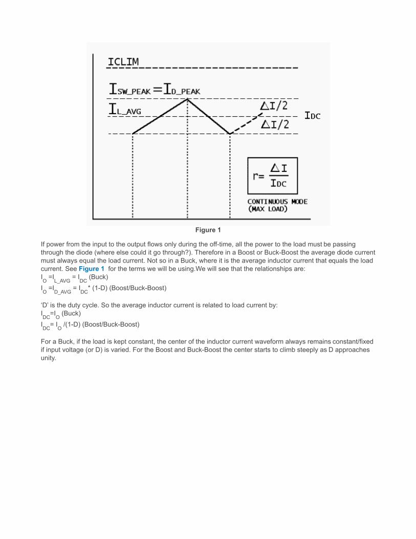
Figure 1
If power from the input to the output flows only during the off-time, all the power to the load must be passingthrough the diode (where else could it go through?). Therefore in a Boost or Buck-Boost the average diode currentmust always equal the load current. Not so in a Buck, where it is the average inductor current that equals the loadcurrent. See Figure 1 for the terms we will be using.We will see that the relationships are:IO
=IL_AVG
= IDC
(Buck)
IO
=ID_AVG
= IDC
* (1-D) (Boost/Buck-Boost)
‘D’ is the duty cycle. So the average inductor current is related to load current by:IDC
=IO
(Buck)
IDC
= IO
/(1-D) (Boost/Buck-Boost)
For a Buck, if the load is kept constant, the center of the inductor current waveform always remains constant/fixedif input voltage (or D) is varied. For the Boost and Buck-Boost the center starts to climb steeply as D approachesunity.
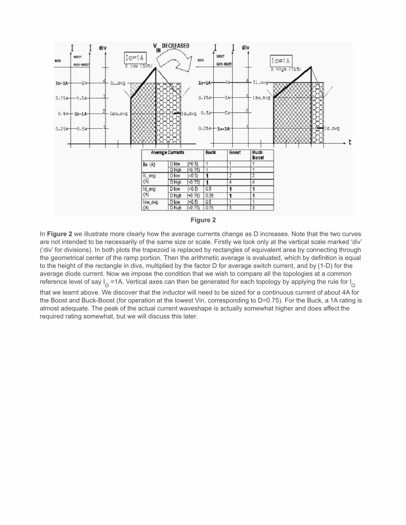
Figure 2
In Figure 2 we illustrate more clearly how the average currents change as D increases. Note that the two curvesare not intended to be necessarily of the same size or scale. Firstly we look only at the vertical scale marked ‘div’(‘div’ for divisions). In both plots the trapezoid is replaced by rectangles of equivalent area by connecting throughthe geometrical center of the ramp portion. Then the arithmetic average is evaluated, which by definition is equalto the height of the rectangle in divs, multiplied by the factor D for average switch current, and by (1-D) for theaverage diode current. Now we impose the condition that we wish to compare all the topologies at a commonreference level of say I
O =1A. Vertical axes can then be generated for each topology by applying the rule for I
Othat we learnt above. We discover that the inductor will need to be sized for a continuous current of about 4A forthe Boost and Buck-Boost (for operation at the lowest Vin, corresponding to D=0.75). For the Buck, a 1A rating isalmost adequate. The peak of the actual current waveshape is actually somewhat higher and does affect therequired rating somewhat, but we will discuss this later.
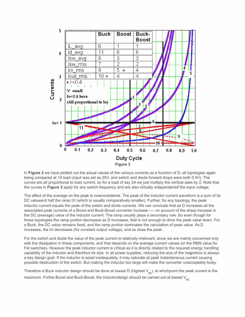
Figure 3
In Figure 3 we have plotted out the actual values of the various currents as a function of D, all topologies againbeing compared at 1A load (input was set as 20V, and switch and diode forward drops were both 0.5V). Thecurves are all proportional to load current, so for a load of say 2A we just multiply the vertical axes by 2. Note thatthe curves in Figure 3 apply for any switch frequency and are also virtually independentof the input voltage.
The effect of the average on the peak is nowconsidered. The peak of the inductor current waveform is a sum of itsDC valueand half the ramp DI (which is usually comparatively smaller). Further, for any topology, the peakinductor current equals the peak of the switch and diode currents. We can conclude that as D increases all theassociated peak currents of a Boost and Buck-Boost converter increase ---- on account of the sharp increase inthe DC (average) value of the inductor current. The ramp usually plays a secondary role. So even though forthese topologies the ramp portion decreases as D increases, that is not enough to drive the peak value down. Fora Buck, the DC value remains fixed, and the ramp portion dominates the calculation of peak value. As Dincreases, the DI decreases (for constant output voltage), and so does the peak.
For the switch and diode the value of the peak current is relatively irrelevant, since we are mainly concerned onlywith the dissipation in these components, and that depends on the average current values (or the RMS value forFet switches). However the peak inductor current is critical as it is directly related to the required energy handlingcapability of the inductor and therefore its size. In all power supplies, reducing the size of the magnetics is alwaysa key design goal. If the inductor is sized inadequately, it may saturate at peak instantaneous current causingpossible destruction of the switch. But making the inductor too large will make the converter unacceptably bulky.
Therefore a Buck inductor design should be done at lowest D (highest VIN
), at whichpoint the peak current is the
maximum. Forthe Boost and Buck-Boost, the inductordesign should be carried out at lowest VIN
.
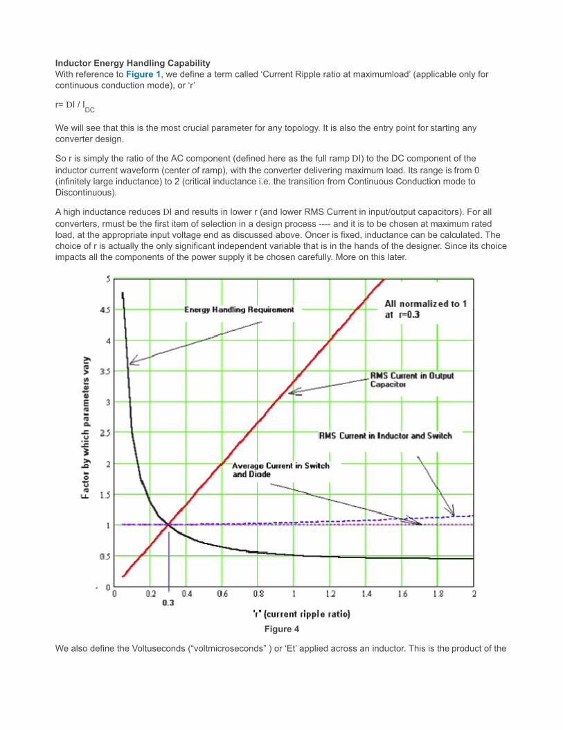
Inductor Energy Handling CapabilityWith reference to Figure 1, we define a term called ‘Current Ripple ratio at maximumload’ (applicable only forcontinuous conduction mode), or ‘r’
r= DI / IDC
We will see that this is the most crucial parameter for any topology. It is also the entry point for starting anyconverter design.
So r is simply the ratio of the AC component (defined here as the full ramp DI) to the DC component of theinductor current waveform (center of ramp), with the converter delivering maximum load. Its range is from 0(infinitely large inductance) to 2 (critical inductance i.e. the transition from Continuous Conduction mode toDiscontinuous).
A high inductance reduces DI and results in lower r (and lower RMS Current in input/output capacitors). For allconverters, rmust be the first item of selection in a design process ---- and it is to be chosen at maximum ratedload, at the appropriate input voltage end as discussed above. Oncer is fixed, inductance can be calculated. Thechoice of r is actually the only significant independent variable that is in the hands of the designer. Since its choiceimpacts all the components of the power supply it be chosen carefully. More on this later.
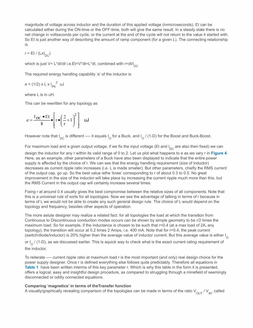
Figure 4
We also define the Voltuseconds (“voltmicroseconds” ) or ‘Et’ applied across an inductor. This is the product of the
magnitude of voltage across inductor and the duration of this applied voltage (inmicroseconds). Et can becalculated either during the ON-time or the OFF-time, both will give the same result. In a steady state there is nonet change in voltseconds per cycle, or the current at the end of the cycle will not return to the value it started with.So Et is just another way of describing the amount of ramp component (for a given L). The connecting relationshipis
r = Et / (LxIDC
)
which is just V= L*dI/dt i.e.Et=V*dt=L*dI, combined with r=dI/IDC
The required energy handling capability ‘e’ of the inductor is
e = (1/2) x L x IPK
2 uJ
where L is in uH.
This can be rewritten for any topology as
However note that IDC
is different ---- it equals IO
for a Buck, and IO
/ (1-D) for the Boost and Buck-Boost.
For maximum load and a given output voltage, if we fix the input voltage (Et and IDC
are also then fixed) we can
design the inductor for any r within its valid range of 0 to 2. Let us plot what happens to e as we vary r in Figure 4.Here, as an example, other parameters of a Buck have also been displayed to indicate that the entire powersupply is affected by the choice of r. We can see that the energy handling requirement (size of inductor)decreases as current ripple ratio increases (i.e. L is made smaller). But other parameters, chiefly the RMS currentof the output cap, go up. So the best value isthe ‘knee’ corresponding to r of about 0.3 to 0.5. No greatimprovement in the size of the inductor will take place by increasing the current ripple much more than this, butthe RMS Current in the output cap will certainly increase several times.
Fixing r at around 0.4 usually gives the best compromise between the relative sizes of all components. Note thatthis is a universal rule of sorts for all topologies. Now we see the advantage of talking in terms of r because interms of L we would not be able to create any such general design rule. The choice of L would depend on thetopology and frequency, besides other aspects of operation.
The more astute designer may realize a related fact: for all topologies the load at which the transition fromContinuous to Discontinuous conduction modes occurs can be shown by simple geometry to be r/2 times themaximum load. So for example, if the inductance is chosen to be such that r=0.4 (at a max load of 2A, anytopology), the transition will occur at 0.2 times 2 Amps, i.e. 400 mA. Note that for r=0.4, the peak current(switch/diode/inductor) is 20% higher than the average value of inductor current. But this average value is either I
Oor I
O / (1-D), as we discussed earlier. This is aquick way to check what is the exact current rating requirement of
the inductor.
To reiterate ---- current ripple ratio at maximum load r is the most important (and only) real design choice for thepower supply designer. Once r is defined everything else follows quite predictably. Therefore all equations inTable 1 have been written interms of this key parameter r. Which is why this table in the form it is presented,offers a logical, easy and insightful design procedure, as compared to struggling through a minefield of seeminglydisconnected or oddly connected equations.
Comparing ‘magnetics’ in terms of theTransfer functionA visually/graphically revealing comparison of the topologies can be made in terms of the ratio V
OUT / V
IN, called

‘x’ here. This term intuitively indicates ‘how hard’ the converter is working at doing its job. x=1 corresponds toswitch-fully-closed condition for a Buck, or switch-fully-open for a Boost, or a switch operating at 50% duty cyclefor a Buck-Boost. x can theoretically lie between 0 and 1 for a Buck, between 1 to ¥ for a Boost and from 0 to ¥ forthe Buck-Boost.
Note that high x corresponds to low VIN
. So a high x corresponds to a high duty cycle forall the topologies.
What happens to the energy handling capability (for a given r) as a function of x? Also, does a Boost typicallyrequire a larger inductance than a Buck-Boost?
Using Table 1, we can plot out these resultsin Figure 5. We can see that (for a given x), the size of the inductorand the required inductance (for r=0.4) increases 10 times for a tenfold increase in input voltage OR a tenfolddecrease in frequency.
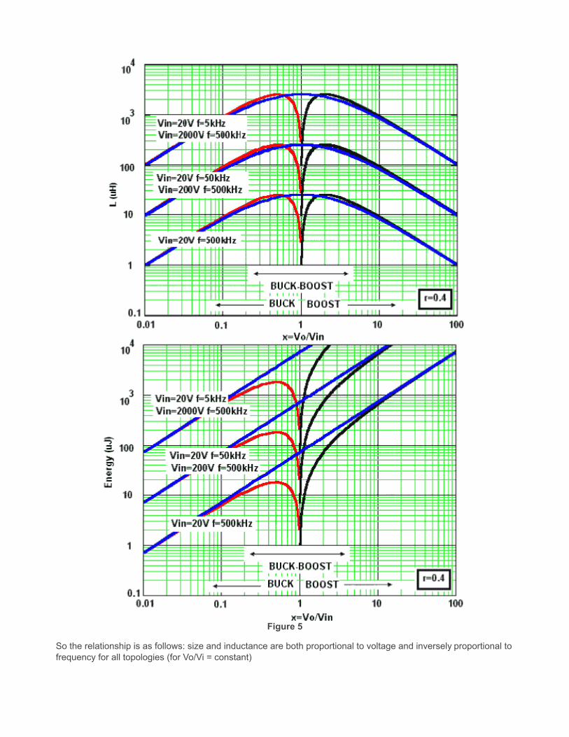
Figure 5
So the relationship is as follows: size and inductance are both proportional to voltage and inversely proportional tofrequency for all topologies (for Vo/Vi = constant)

The buck requires the largest inductors for a duty cycle (VOUT
/VIN
= x = D) of 0.5. For all others, increasing x (i.e.
higher D) means alarger inductor.
For inductance, all topologies call for the maximum inductance at VIN_50
(which is the input voltage for which the
duty cycle is 50%--- from the figure check backwards using the definition of x). Note that for small x, the inductorsize and inductance of a Buck-Boost approximates a Buck, and at high x, the Buck-Boost approximates the Boost.
Some of the above conclusions we may have already ‘known’ from gut feel (or a previous life). But especiallywhere magnetics design is concerned, engineers are warned against relying completely on instincts or intuition, asthis is often very misleading (See also References a and b).
In fact, the designer who feels he has understood all the above conclusions, now needs to realize that going froma curve of say 20V/500kHz to the upper one of 200V/500kHz, keeping x constant is easier said than done. It is notthe same as the usual condition of VO =constant. So does the required inductance really change?? Intuition…..?!
Lastly, we note that Figure 5 is drawn up to serve as a design chart. It does not directly reveal what happens to agiven power supply as input voltage is changed. Therefore r is fixed at 0.4 for all the curves in Figure 5. Whereasin an actual power supply, as we change input voltage r changes. The actual variations of a real power supply inresponse to changes ininput voltage will be discussed in the next section.
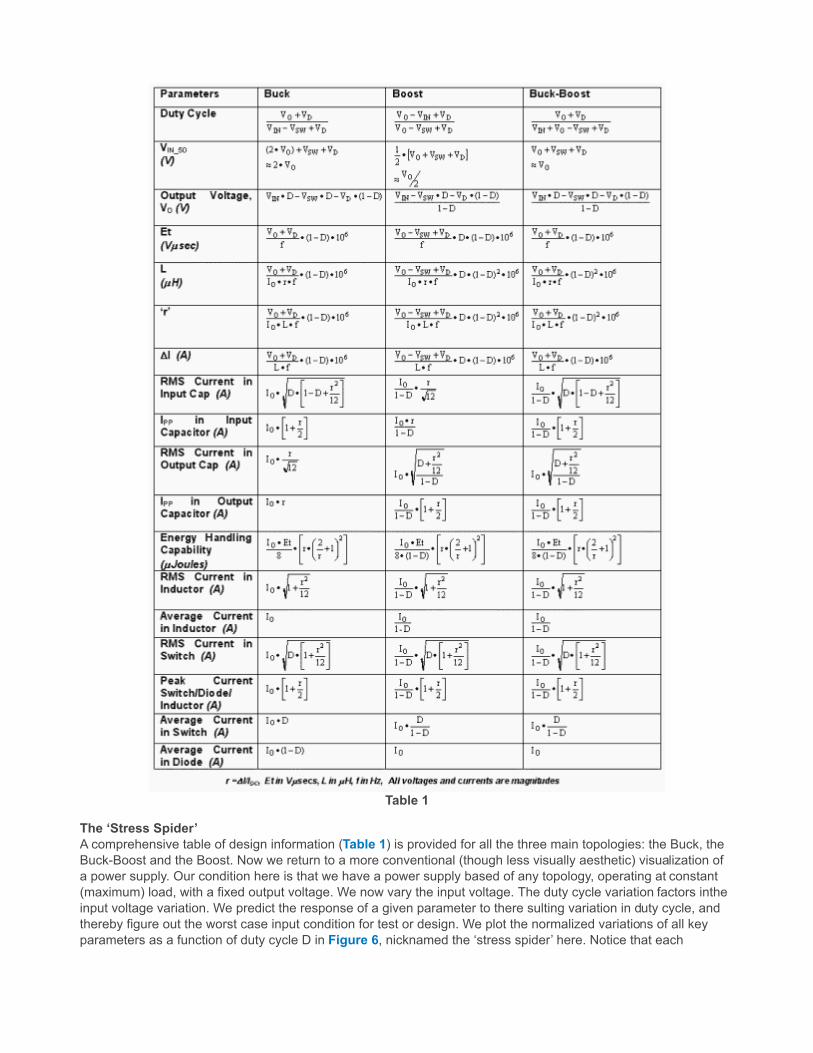
Table 1
The ‘Stress Spider’A comprehensive table of design information (Table 1) is provided for all the three main topologies: the Buck, theBuck-Boost and the Boost. Now we return to a more conventional (though less visually aesthetic) visualization ofa power supply. Our condition here is that we have a power supply based of any topology, operating at constant(maximum) load, with a fixed output voltage. We now vary the input voltage. The duty cycle variation factors intheinput voltage variation. We predict the response of a given parameter to there sulting variation in duty cycle, andthereby figure out the worst case input condition for test or design. We plot the normalized variations of all keyparameters as a function of duty cycle D in Figure 6, nicknamed the ‘stress spider’ here. Notice that each
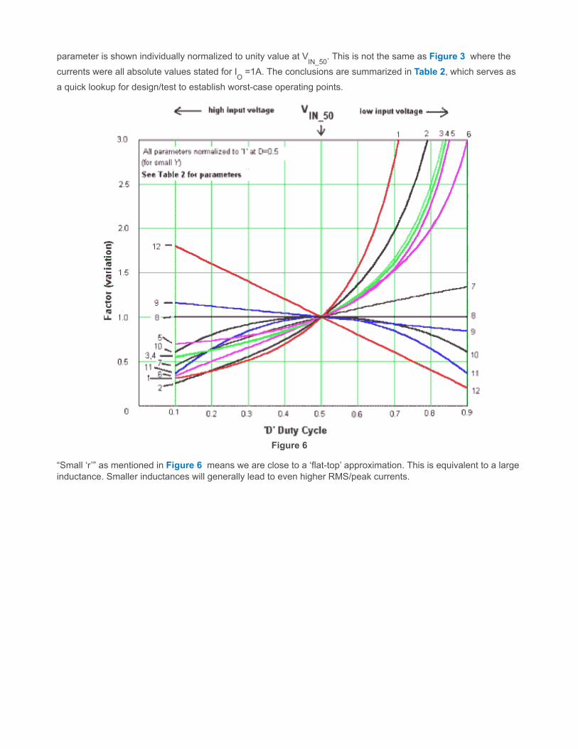
parameter is shown individually normalized to unity value at VIN_50
. This is not the same as Figure 3 where the
currents were all absolute values stated for IO
=1A. The conclusions are summarized in Table 2, which serves as
a quick lookup for design/test to establish worst-case operating points.
Figure 6
“Small ‘r’” as mentioned in Figure 6 means we are close to a ‘flat-top’ approximation. This is equivalent to a largeinductance. Smaller inductances will generally lead to even higher RMS/peak currents.
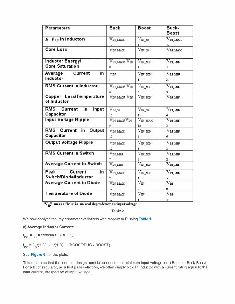
Table 2
We now analyze the key parameter variations with respect to D using Table 1.
a) Average Inductor Current:
IDC
= IO
= constan t (BUCK)
IDC
= [IO
/(1-D)] µ 1/(1-D) (BOOST/BUCK-BOOST)
See Figure 6 for the plots.
This reiterates that the inductor design must be conducted at minimum input voltage for a Boost or Buck-Boost.For a Buck regulator, as a first pass selection, we often simply pick an inductor with a current rating equal to theload current, irrespective of input voltage.

b) Inductor ramp current
For all topologies, this AC component is completely responsible for the core loss (which does not depend on IDC
,
provided the inductor is not saturating).
Now, for all the topologies, there is an applied voltage ‘VON
’ across the inductor when the switch is ON. This
causes acertain AC ramp component ‘DI’ across the inductor from the basic equation VON
=L*DI/(D/f) or
DI=VON
*D/(L*f), where f is the frequency. As the input voltage falls, VON
also decreases, but D increases. So what
is the net effect on DI? From Table 1
DI µ (1 - D) (BUCK/BUCK-BOOST)DI µ D • (1 - D) (BOOST)
See Figure 6 for the plots.
If the input voltage range does not include VIN_50
, we must choose either VIN_MIN
or VIN_MAX
, whichever happens
to be closer to VIN_50
.
c) Current Ripple ratio at max load ‘r’
r = (DI/IDC
) = (DI/IO
) (BUCK)
r = (DI/IDC
) = (DI/IO
) • (1-D) (BOOST/BUCK-BOOST)
See Figure 6 for the plots.
The formal design procedure for any converter design can now be summarized:
First the inductor design is to be done. This is to be performed at lowest input for a Boost and Buck-Boost, and athighest input voltage for a Buck, by choosing r to be about 0.4. Then L can be calculated using Table 1. Since rvaries as the input voltage changes, it can be recalculated at any input voltage, again by using Table 1 and the Lwe have calculated. So if we are interested in finding the value of any parameter at any another specific inputvoltage, we can use the required equation from Table 1. But we might find that that requires an input value for r.The value of r to be used here must be the (recalculated) value of r at that particular input voltage. Figure 6 willquickly indicate what input voltage is to be used if we want the worst-case value for the parameter.
d) Input Capacitor RMS current
This determines the basic/minimum selection criterion for the input capacitor since the capacitor must be rated atleast for the worst case RMS current that will pass through it. A capacitor operated with an RMS current higherthan its rated value, is not guaranteed to have any specific life by most manufacturers. And any published lifeexpectancy vs. temperature curves/equations may not be valid.
For small r, we can see that this goes as

See Figure 6 for the plots.
So the temperature of the capacitor must also be evaluated at the correct input voltages. Again, if the inputvoltage range does not include V
IN_50, we must choose either V
IN_MIN or V
IN_MAX, whichever happens to be closer
to VIN_50
.
e) Output Capacitor RMS Current
For small r, we can see that this goes as
See Figure 6 for the plots.
So the temperature of the output capacitor must also be evaluated at the correct input voltage.
f) Output Peak to Peak Current
We are also concerned with the peak to peak current, IPP_OUT
through the output capacitor as this determines the
output voltage ripple. DVOUT
=IPP_OUT
*ESROUT
, where ESROUT
is the Equivalent Series Resistance of the output
capacitor. This output ripple is a major component of the noise spectrum at the output of the power supply.
For small r, we can see that this goes as
IPP_OUT
µ r µ (1-D) (BUCK)
IPP_OUT
µ (1/(1-D)) (BOOST/BUCK-BOOST)
So,IPP_OUT
---> maximum at highest input voltage for Buck
IPP_OUT
---> maximum at lowest inputvoltage for Boost/Buck-Boost
g) Switch RMS Current
For a MOSFET switch we need to calculate the conduction loss as given by I2 RMS
*rds. The crossover losses are
lowest at the minimum input voltage. But since they are usually a small fraction of the conduction losses, they areignored here. The IRMS ofthe switch varies in the following manner
For small r, we can see that this goes as
Plotting these out in Figure 6 we can see that
IRMS
---> maximum at lowest input voltagefor Buck/Boost/Buck-Boost
Note that for a Buck, the dissipation in the switch goes up only slightly at low input voltages, but for the remainingtopologies,the dissipation goes up quite steeply at low input voltages, leading to a large drop inefficiency. In Table1, the average switch current is also provided, for calculation of dissipation in bipolar switches.
h) Average Diode CurrentFor a diode we need to calculate the forward loss as given by V
D * I
D_AVG, where ‘V
D’ is the drop across the diode
when it conducts. For the Boost and the Buck-Boost, the average diode current is the load current, so it is notgoing to change with duty cycle. But for the Buck it does vary.
ID_AVG
µ (1-D) (BUCK)
ID_AVG
µ constan t (BOOST/BUCK-BOOST)
See Figure 6 for the plots.
We know that the dissipation in the switch of a Buck remains relatively constant as input voltage increases(ignoring crossover losses), but now we see that the diode dissipation increases as we do so. So we expect theefficiency of a Buck regulator to fall at high input voltages on account of increased diode dissipation (assumingVSW<V
D where VSW is the forward drop across the switch). For the Boost and Buck-Boost, the diode dissipation
does not change as input voltage falls, but the switch dissipation increases dramatically. So we expect theefficiency of a Boost or a Buck-Boost to fall at low input voltages on account of increased switch dissipation(unless crossover losses are very large, in which case the reverse is occasionally found to be true).
For testing diode temperature, we need to test a Buck regulator at the highest input voltage. For the othertopologies, it does not matter much. This is indicated as ‘V
IN’ in Table 2, implying any input voltage should be OK
to design to or for test.
i) Inductor Energy
For our analysis here, we first make an approximation for the rather complicated term in Table 1 for ‘e’ involving r.Assuming r to be small this term becomes
Then

See Figure 6 for the plots. They are what we expected from previous discussions.
j) Average Inductor Current
If r is small, the average and RMS values of the inductor current are the same, ‘IL’. The copper loss in the inductor
is IL2*R, where r is the winding resistance. This loss is usually very large compared to the core loss (which
depends on DI, as discussed earlier), and it largely determines the temperature rise of the inductor.
For small r, we can see that the RMS/Avg current goes as
IL µ constan t (BUCK)
IL µ (1/(1-D)) (BOOST/BUCK-BOOST)
See Figure 6 for the plots.
k) Peak Switch Current
This parameter is important because every controller has a current limit for the switch, and if the calculated peakexceeds the lowest value possible of the switch current limit, anywhere in the input voltage range, the requiredoutput power cannot be delivered. The peak current in a Buck is just a little higher than the load current, and so forexample, the LM2593HV ‘Step Down (Buck) regulator’ IC from National Semiconductor, which is designed for ‘2Aload’, has a minimum set value of 2.3A for the switch current limit. Yet, as seen from the datasheet of this device,this Buck IC can be operated as a ‘positive to negative’ regulator, which is actually a standard Buck-Boosttopology. In this mode, the peak current is much higher, and it depends on the duty cycle/input voltage too. So itmay not be possible to get 2A load.
For small r, we can see that the peak currentgoes as:
See Figure 6 for the plots.

Therefore Current Limiting must be ruled out at minimum input voltage for the Boost and Buck-Boost, but for theBuck we must go to the highest input voltage.
Summing UpThe visualizations and curves presented are an important part of trying to understand the topologies. Thetransformer-based topologies are not much different. For example the flyback has a design parameter called ‘V
OR’
or reflected output voltage (= VO
* (Np/Ns)) which is actually the output voltage of an equivalent Buck-Boost. The
more experienced designer can easily extend the concepts presented here to transformer-based topologies. The‘mentalpicture’ hopefully acquired here, also applies to them.
Referencesa) “Off-the-shelf Inductors for Buck-converters” by Sanjaya Maniktala, Electronic Engineering, August2001b) “Current Ripple Ratio Simplifies Selection of Off-the-shelf Inductors for Buck-converters” by Sanjaya Maniktala,Power Electronics Technology, October2001c) “Reducing Converter Stresses - Part 1” by Sanjaya Maniktala Power Electronics Technology, May 2002d) “Reducing Converter Stresses - Part 2” by Sanjaya Maniktala Power Electronics Technology, July 2002e) http://power.national.com

IMPORTANT NOTICE
Texas Instruments Incorporated and its subsidiaries (TI) reserve the right to make corrections, modifications, enhancements, improvements,and other changes to its products and services at any time and to discontinue any product or service without notice. Customers shouldobtain the latest relevant information before placing orders and should verify that such information is current and complete. All products aresold subject to TI’s terms and conditions of sale supplied at the time of order acknowledgment.
TI warrants performance of its hardware products to the specifications applicable at the time of sale in accordance with TI’s standardwarranty. Testing and other quality control techniques are used to the extent TI deems necessary to support this warranty. Except wheremandated by government requirements, testing of all parameters of each product is not necessarily performed.
TI assumes no liability for applications assistance or customer product design. Customers are responsible for their products andapplications using TI components. To minimize the risks associated with customer products and applications, customers should provideadequate design and operating safeguards.
TI does not warrant or represent that any license, either express or implied, is granted under any TI patent right, copyright, mask work right,or other TI intellectual property right relating to any combination, machine, or process in which TI products or services are used. Informationpublished by TI regarding third-party products or services does not constitute a license from TI to use such products or services or awarranty or endorsement thereof. Use of such information may require a license from a third party under the patents or other intellectualproperty of the third party, or a license from TI under the patents or other intellectual property of TI.
Reproduction of TI information in TI data books or data sheets is permissible only if reproduction is without alteration and is accompaniedby all associated warranties, conditions, limitations, and notices. Reproduction of this information with alteration is an unfair and deceptivebusiness practice. TI is not responsible or liable for such altered documentation. Information of third parties may be subject to additionalrestrictions.
Resale of TI products or services with statements different from or beyond the parameters stated by TI for that product or service voids allexpress and any implied warranties for the associated TI product or service and is an unfair and deceptive business practice. TI is notresponsible or liable for any such statements.
TI products are not authorized for use in safety-critical applications (such as life support) where a failure of the TI product would reasonablybe expected to cause severe personal injury or death, unless officers of the parties have executed an agreement specifically governingsuch use. Buyers represent that they have all necessary expertise in the safety and regulatory ramifications of their applications, andacknowledge and agree that they are solely responsible for all legal, regulatory and safety-related requirements concerning their productsand any use of TI products in such safety-critical applications, notwithstanding any applications-related information or support that may beprovided by TI. Further, Buyers must fully indemnify TI and its representatives against any damages arising out of the use of TI products insuch safety-critical applications.
TI products are neither designed nor intended for use in military/aerospace applications or environments unless the TI products arespecifically designated by TI as military-grade or "enhanced plastic." Only products designated by TI as military-grade meet militaryspecifications. Buyers acknowledge and agree that any such use of TI products which TI has not designated as military-grade is solely atthe Buyer's risk, and that they are solely responsible for compliance with all legal and regulatory requirements in connection with such use.
TI products are neither designed nor intended for use in automotive applications or environments unless the specific TI products aredesignated by TI as compliant with ISO/TS 16949 requirements. Buyers acknowledge and agree that, if they use any non-designatedproducts in automotive applications, TI will not be responsible for any failure to meet such requirements.
Following are URLs where you can obtain information on other Texas Instruments products and application solutions:
Products Applications
Audio www.ti.com/audio Communications and Telecom www.ti.com/communications
Amplifiers amplifier.ti.com Computers and Peripherals www.ti.com/computers
Data Converters dataconverter.ti.com Consumer Electronics www.ti.com/consumer-apps
DLP® Products www.dlp.com Energy and Lighting www.ti.com/energy
DSP dsp.ti.com Industrial www.ti.com/industrial
Clocks and Timers www.ti.com/clocks Medical www.ti.com/medical
Interface interface.ti.com Security www.ti.com/security
Logic logic.ti.com Space, Avionics and Defense www.ti.com/space-avionics-defense
Power Mgmt power.ti.com Transportation and Automotive www.ti.com/automotive
Microcontrollers microcontroller.ti.com Video and Imaging www.ti.com/video
RFID www.ti-rfid.com
OMAP Mobile Processors www.ti.com/omap
Wireless Connectivity www.ti.com/wirelessconnectivity
TI E2E Community Home Page e2e.ti.com
Mailing Address: Texas Instruments, Post Office Box 655303, Dallas, Texas 75265Copyright © 2011, Texas Instruments Incorporated


![Analysis and Comparison of dc/dc Topologies in …dc/dc converters with high voltage gain is performed [8]. Based on the analysis and the system specifications, the topology selection](https://img.pdfslide.net/doc/110x75/5fc8087983914757f363b823/analysis-and-comparison-of-dcdc-topologies-in-dcdc-converters-with-high-voltage.jpg)


![IBM technology symposium 11032012.ppt · Converter Topologies. R1 R DC 1 DC CR ... Resonant Frequency modulated LLC (1) ... IBM_technology_symposium_11032012.ppt [Compatibility Mode]](https://img.pdfslide.net/doc/110x75/5b1db8607f8b9ab06b8be177/ibm-technology-symposium-converter-topologies-r1-r-dc-1-dc-cr-resonant.jpg)


![Prof. S. Ben-Yaakov , DC-DC Converters [2- 1] BUCK, BOOST ...dcdc/slides/DC-DC part 2_Double.pdf · 2.3 Buck-Boost converter 2.4 Comparison between topologies ... Prof. S. Ben-Yaakov](https://img.pdfslide.net/doc/110x75/5aa2963f7f8b9ac67a8d4acf/prof-s-ben-yaakov-dc-dc-converters-2-1-buck-boost-dcdcslidesdc-dc.jpg)